
4 Optimization of Organic Photovoltaic Cells
Fanan Wei, Liming Liu and Guangyong Li
CONTENTS
4.2 Optimizing Device Thickness via Optical Modeling and Electrical Simulation
4.3 Optimizing Device via Multiscale Simulation
4.1 Introduction
With the advantages of being low cost, lightweight and flexible, organic photovoltaics are becoming a promising technology for sustainable energy harvesting. As a result of the continuous efforts of the worldwide research community, the current power conversion efficiency (PCE) record of organic photovoltaic cells has reached 12% [1] and the projected lifetime is more than 7 years [2]. Nevertheless, almost all advancements in organic photovoltaics so far have been from trial-and-error experiments. Because of the complexity of organic photovoltaic cells, it is not possible to simply tune one or a few parameters to achieve optimal performance. Further advancement in organic photovoltaics will be a daunting challenge, considering the nearly infinite number of material combinations and processing conditions that can affect device performance. Compared to trial-and-error-based physical experiments, computational modeling and simulation is a more effective and economical way to optimize devices for best performance. In Chapter 3, we described the optical and electrical modeling and simulation of organic photovoltaic cells. If these approaches can be combined to include all aspects of organic photovoltaic cells in the model, optimization of organic photovoltaic cells will be possible. In this chapter, we describe how organic photovoltaic cells are optimized for best performance via simulations. The poly-3-hexyl-thiophene (P3HT):phenyl-C61-butyric acid methylester (PCBM) material system is used as an example to demonstrate the effectiveness of optimization via simulation. The P3HT:PCBM system is chosen simply because it is commonly investigated in the literature and many parameters are readily available. The methods described herein could be applied to any other type of organic photovoltaic cells without any technical barriers.
4.2 Optimizing Device Thickness via Optical Modeling and Electrical Simulation
Carrier mobility is one of the important factors that dictate the performance of the photovoltaic cells. It has been found that carrier mobility in organic photovoltaic cells can be improved by ameliorating the nanoscale morphology of the active layer through thermal annealing [3-6] and solvent annealing [6-8]. The improved carrier mobility is largely due to the improved crystallinity and phase separation, which has been proven with XRD (x-ray diffraction) and TEM [3]. Table 4.1 shows the typical carrier mobility collected from the literature under different annealing conditions. Clearly, carrier mobility, especially hole mobility, can be significantly improved through thermal annealing. These parameters can be used to predict device performance via simulation.
In Chapter 3, we developed an optical model to calculate the photon absorption of organic photovoltaic cells based on optical transfer matrix. By taking the interference effect into consideration, the optical transfer matrix can be used to compute the optical electric field and subsequently light intensity distribution in organic photovoltaic cells. By integrating the energy dissipation rate for light wavelength between 350 nm and 800 nm (effective absorption range for P3HT), the photon absorption efficiency under standard AM 1.5G illumination with respect to the thickness of the P3HT:PCBM layer for a device with the structure ITO(150 nm)/PEDOT:PSS(40 nm)/P3HT:PCBM-/Al(100 nm) can be acquired as shown in Figure 4.1. Clearly, there exist absorption peaks due to the interference, which means the maximum power conversion efficacy will be very sensitive to the thickness of the active layer.
TABLE 4.1 Carrier Mobility for Figure 4.2 Simulation
MobilityDevice |
As-cast |
Annealed at 70°C |
Annealed at 140°C |
μn (cm2/Vs) |
2 × 10⁻⁴ |
1 × 10⁻³ |
2.5 × 10⁻³ |
μp (cm2/Vs) |
4 × 10⁻⁸ |
1 × 10⁻⁶ |
3 × 10⁻⁴ |
By combining optical modeling and electrical simulation using drift-diffusion model as described in Chapter 3, we are able to optimize the thickness of organic photovoltaic cells by simulating J−V curves for devices with different thicknesses and then by extracting parameters such as short-circuit current density (Jsc), open-circuit voltage (Voc), fill factor (FF), and power conversion efficiency (PCE) as a function of the thickness of the active layer. Figure 4.2 shows the simulation results for P3HT:PCBM solar cell devices with different post-treatments: as-casted (solid curve), annealed at 70°C (dotted dash curve), and annealed at 140°C for one half hour (dotted curve), respectively. The PCE shown in Figure 4.2 gives different peak locations for different devices. There are two observations regarding the PCE in Figure 4.2: First, the PCE increases with the increase in carrier mobility (Table 4.1), irrespective of the thickness of the active layer; second, with the increased carrier mobility, the thickness value at which PCE gets maximum value increased as indicated by the arrow in the inset because high carrier mobility can guarantee sufficient carrier extraction when increasing the thickness. Compared with the other two devices, the increased performance of the device annealed at 140°C is mainly due to the increased carrier mobility [9,10]. Therefore, the location of the optimal thickness is also determined by the carrier mobility and hence this simulation is indispensable to optimizing the thickness of organic photovoltaic cells. The simulation results agree well with the results reported in the literature that the best device performance is located at either thickness around 90 nm or 220 nm.
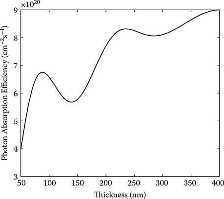
FIGURE 4.1
Photon absorption efficiency versus the thickness of the active layer.
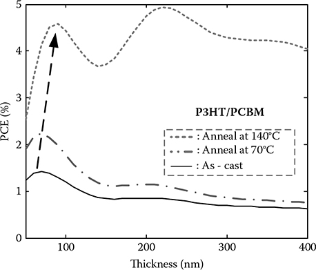
FIGURE 4.2
Thickness-dependent performance of P3HT/PCBM photovoltaic cells.
4.3 Optimizing Device via Multiscale Simulation
Nanoscale morphology of the active layer is the main factor that dictates carrier mobility, and thus device performance. The optimization in the last section combines only the optical model and the electrical simulation based on a drift and diffusion model, and thus is unable to directly take nanoscale morphology into account. A multiscale simulation strategy that integrates Monte Carlo simulation with optical absorption calculation and macroscopic simulation will be a suitable approach to simulate the performance of organic photovoltaic cells. Such integration takes into account the multiscale aspects of the device such as the active layer thickness, nanoscale morphology, and the weight ratio of donor/acceptor. Thus, it is effective in optimizing several physical aspects of the device simultaneously. In this section, we describe the details of optimizing the device via this multiscale simulation.
The schematic diagram of the proposed multiscale modeling and simulation framework, illustrated in Figure 4.3, is composed of four modules:
Morphology Generation Module: The morphology generation module constructs the nanoscale morphology of the bulk heterojunctions according to the weight ratio of D/A as well as other constraints and parameters such as annealing conditions.
Monte Carlo Simulation Module: The Monte Carlo simulation module calculates the recombination ratio, exciton-dissociation efficiency, and the bulk (apparent or effective) mobility corresponding to the internal morphology and the internal electrical field.
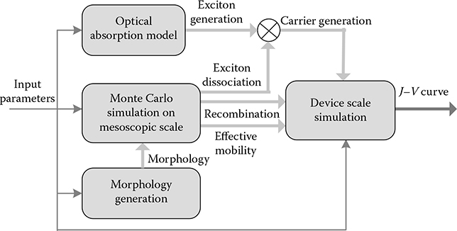
FIGURE 4.3
Schematic of multiscale simulation of organic photovoltaic cells with bulk heterojunctions.Carrier Generation Calculation Module: The carrier generation calculation module obtains the free charge carrier generation rate by multiplying the exciton-dissociation efficiency (EDE) obtained from the Monte Carlo simulation and the light absorption efficiency calculated from an optical absorption model based on the active layer thickness and the D/A weight ratio.
Macroscopic Simulation Module: Those intermediate parameters obtained from previous modules are fed into the macroscopic simulation module that predicts the current-voltage responses (J−V curves) of a device by considering the physical dimension and boundary conditions as well as other properties of the device. The performances of the device such as the short-circuit current, the open-circuit voltage, the fill factor, and the power conversion efficiency (PCE) are derived from these J−V curves.
During the Monte Carlo simulation, the trajectories of particles (exciton, electron, and hole) are completely recorded for postanalysis. Several variables can be estimated when the simulation reaches a stable state The effective carrier mobility (bulk mobility), the exciton EDE, and the recombination rate are calculated from the following equations:
where lfield is hopping distance in the direction of the electric field, τ is total time expired for hopping, F is the electric field, F = (Δφ-Vext)/d, in which Vext is the applied external voltage, and d is thickness; nex_diss is the number of dissociated excitons, and nrecom_pair is the number of recombined charge carrier pairs.
By varying the external applied voltage and domain size (the size of the minority component) of the active layer, the dependence of bulk mobility on electric field and morphology for different weight ratios of the P3HT:PCBM active layer can be determined from the Monte Carlo simulation. To improve the accuracy, each data point is obtained by averaging results from at least three repeated simulations under the same conditions. The simulation results demonstrate that the effective (bulk) mobility increases when the domain size increases (Figures 4.4a and 4.5a) because the barrier is less for carriers to move toward the corresponding electrode. The effective mobility decreases when the electric field increases (Figures 4.4b and 4.5b) because it is more difficult for carriers to escape from dead-end traps under high electric field strength. The result agrees well with that from the experiment [11]. It is also clear that when the concentration of PCBM is higher, a higher electron mobility is observed, while a higher concentration of P3HT leads to a higher hole mobility, which is intuitive and straightforward.

FIGURE 4.4
Dependences of effective electron mobility (bulk electron mobility) on (a) domain size and (b) electric field. The legend shows the corresponding D/A weight ratio.
The recombination rates corresponding to the electric field and morphology for different weight ratios are shown in Figure 4.6. The recombination rate shows a declining tendency to both domain size and electric field strength. As the domain size increases, the transport paths for carriers become wider, and the carriers are more likely to travel to the electrodes rather than being recombined at the donor/acceptor interface. Under a stronger electric field, the carriers can move to electrodes more quickly, so the recombination rate is expected to decrease when the electric field strength increases. It is observed that the 2:3 weight ratio gives the least recombination rate.
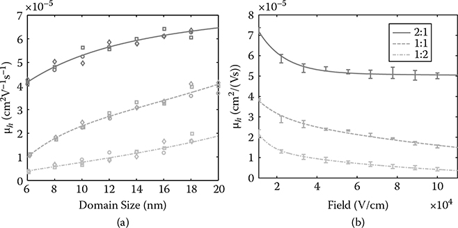
FIGURE 4.5
Dependencies of effective hole mobility (bulk hole mobility) on (a) domain size and (b) field. The legend shows the corresponding D/A weight ratio.
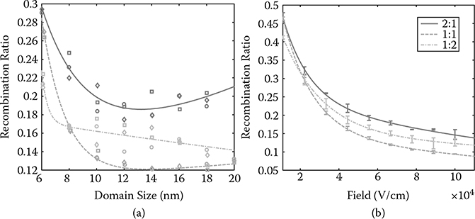
FIGURE 4.6
Dependencies of the recombination ratio on (a) domain size and (b) field. The legend shows the corresponding D/A weight ratio.
The dependence of EDE on domain size is also calculated in the simulation (Figure 4.7). It can be seen that the EDE decreases as domain size increases. Such a trend is reasonable because larger domain size means less interfacial area and thus lower EDE. Apparently, the 1:1 ratio yields the best EDE, which is the reason why the 1:1 ratio often gives the best experimental results.
The photon absorption rate can be computed through integration of the energy dissipation rate for light wavelength between 350 nm and 800 nm according to the extinction coefficients for materials with different D/A weight ratios (Figure 4.8). The selected wavelength range (350 nm–800 nm) is reasonable because the light below 350 nm is strongly absorbed by the glass substrate, and the light above 800 nm is rarely absorbed by an active layer due to the large band gap (1.9 eV) of P3HT. For simplification, the dependence of the photon extinction coefficient on the morphology or domain size of the active layer is not taken into consideration here. Some literature [8,10] has reported that the absorption profile changes little after device annealing even though the inner morphology and external quantum efficiency change dramatically. Therefore, it is fair to assume that the photon absorption coefficient remains constant no matter the domain size.
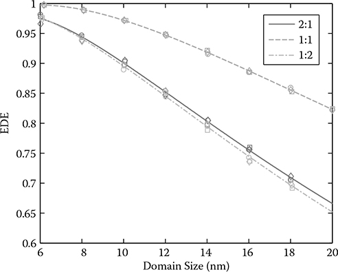
FIGURE 4.7
Dependencies of EDE on the domain size of the active layer. The weight ratio is shown in the legend.
Based on the optical transfer matrix theory [11], we are able to calculate the absorption efficiency of the P3HT:PCBM active layer according to the thickness and D/A weight ratio. Herein, the illumination intensity is set to be the AM 1.5G spectrum. From a Monte Carlo simulation, we have obtained the EDE with respect to domain size (Figure 4.7). If we assume that one absorbed photon transfers into one exciton, the charge carrier generation rate (Figure 4.9) can be obtained now by multiplying the EDE and the photon absorption efficiency.
Even though the internal quantum efficiency, J−V curve and subsequently PCE are obtainable from Monte Carlo simulation directly, Monte Carlo simulation is not a proper choice for a full device description because it does not have a full consideration of the boundary conditions at the electrodes-active layer interfaces. In addition, the Monte Carlo simulation of the J−V curve has a demand for high computation power that is often not readily available. To obtain the J−V curve of the organic photovoltaic cells, we use the macroscopic simulation based on the drift-diffusion model that was discussed in Chapter 3.
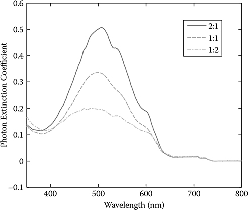
FIGURE 4.8
Photon extinction coefficient for different D/A weight ratio of P3HT:PCBM.
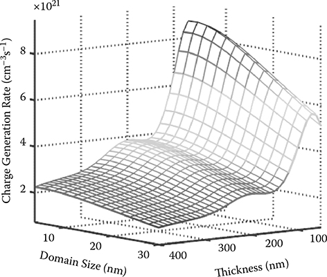
FIGURE 4.9
The dependence of the charge carrier generation rate on both domain size and thickness of an active layer for a device with D/A weight ratio 1:1.
After integration of the simulation modules at each scale, we are able to perform optimization of organic photovoltaic cells via the multiscale simulation. The morphology-dependent parameters, such as bulk mobility, recombination rate, and charge generation rate obtained from Monte Carlo simulation and light absorption calculation, are fed into the macroscopic simulation module to implement a full description of photocurrent generation on the device scale. With the J−V curves obtained from the device scale simulation, subsequent performance indices are calculated. These indices can be used to evaluate the device design and processing conditions for optimal device performance.
In this study, we acquire the current density for the input applied voltage from −0.3 V to 0.7 V with the step of 0.01 V. Furthermore, we vary the thickness of the active layer from 50 nm to 400 nm and the domain size (of the minority component) from 4 nm to 30 nm. The J−V curves corresponding to each point of thickness and domain size and the subsequent device performance parameters are all calculated. As performance dependence on morphology and thickness is predicted, we can locate the maximum PCE value and its corresponding domain size and thickness. Thus, both the inner morphology and the external physical dimension are optimized at the same time.
In order to investigate the influence of the composition of the active layer on the device performance, different morphologies for varied D/A weight ratio (2:1, 1:1, and 1:2) are generated using the Ising model mentioned in Section 3.4. The multiscale simulation is applied to all four groups with different compositions. The dependences of carrier mobility (Figures 4.4 and 4.5) and recombination ratio (Figure 4.6) on domain size and electric field are obtained from the Monte Carlo simulation. With the photon extinction coefficient for different weight ratios, shown in Figure 4.8, the charge generation rates corresponding to different weight ratio are calculated through the optical absorption model (similar to Figure 4.1). Finally, the device performance indices' dependences on domain size and active layer thickness for different weight ratios are calculated and plotted in Figures 4.10a-c. (The results of a 3:1 weight ratio are not shown.)
The influence of D/A composition on the achievable maximum PCE value is shown in Figure 4.11. Table 4.2 lists detailed optimal parameters for each D/A composition. As the weight ratio of P3HT increases, the maximum PCE increases initially, and then the slope decreases, finally decreasing quickly. The tendency is reasonable because the electron and hole mobility are unbalanced initially. Therefore, increasing the weight ratio of P3HT increases the hole mobility and balance of the transport of the two types of carriers. Further, the increase in P3HT composition will lead to the rise of photon absorption efficiency, and result in a higher maximum PCE. Excessively increasing P3HT composition results in a higher recombination rate (Figure 4.6) and thus leads to a dramatic decrease in performance. Surprisingly, the weight ratio 1:1, which has been chosen in many studies, does not yield the best performance but is very close to the best one. Our findings suggest that the best weight ratio of P3HT is close to 2:1
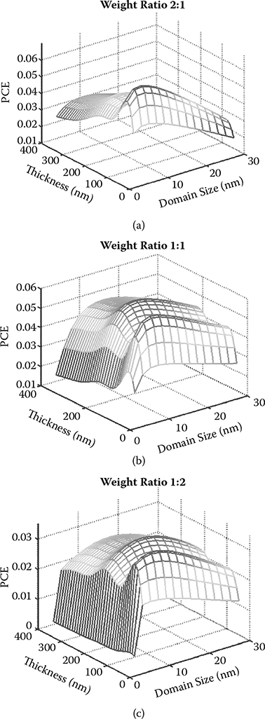
FIGURE 4.10
The dependence of PCE on the domain size and thickness of an active layer for varied D/A composition: (a) 2:1, (b) 1:1, and (c) 1:2.
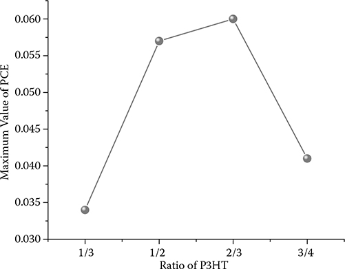
FIGURE 4.11
The maximum value of PCE versus weight ratio of P3HT.
TABLE 4.2 Optimized Parameters under Different Weight Ratios of P3HT:PCBM
Domain Size (nm) |
||||
Weight Ratio |
P3HT |
PCBM |
Thickness (nm) |
Maximum PCE |
3:1 |
24 |
8 |
80 |
4.1% |
2:1 |
16 |
8 |
80 |
6.0% |
1:1 |
10 |
10 |
90 |
5.7% |
1:2 |
10 |
20 |
80 |
3.4% |
From Table 4.2, we can see that the domain sizes of the donor and acceptor are asymmetrical except for the 1:1 ratio. The domain size of the minority component remains constant while the domain size of the counterpart needs to grow with respect to its concentration in order to achieve best device performance. Such kinds of morphology raise a technical challenge to be implemented in reality, which can explain why the 1:1 ratio is reported most often in the literature.
4.4 Discussion and Conclusion
In summary, we first optimized the device thickness by combining the optical model and the electrical simulation based on the drift-diffusion model We then proposed a framework for multiscale modeling and simulation of organic photovoltaic cells with bulk heterojunctions by integrating the Monte Carlo simulation, the photon absorption calculation based on optical transfer matrix theory, and the device scale simulation based on the drift-diffusion model. The multiscale approach is able to account for multiscale aspects of the bulk heterojunctions in the simulation. In this integration, the Monte Carlo simulation engenders exciton-dissociation efficiency, bulk mobility, and recombination rate by taking into account the nanoscale morphology; the outputs of the Monte Carlo simulation are then rendered to the light absorption calculator and the device scale simulator that further generates the complete current-voltage (J−V) characteristics according to the physical dimensions, boundary conditions, and other parameters of the device. The proposed multiscale simulation method can be an efficient tool to simultaneously optimize the thickness, morphology, and D/A composition of the bulk heterojunctions. Even though some parameters used in this simulation may not be completely accurate, the optimization results from such a multiscale simulation approach will provide useful guidance in optimizing the real device through experiments, thus saving a tremendous amount of effort in searching for the optimal parameters. The multiscale simulation is demonstrated for a P3HT:PCBM system in this chapter, but it can be easily extended to other types of organic bulk heterojunctions solar cells as long as the properties of the materials are known.
References
2. C. H. Peters, I. T. Sachs-Quintana, J. P. Kastrop, S. Beaupré, M. Leclerc, and M. D. McGehee, "High efficiency polymer solar cells with long operating lifetimes," Advanced Energy Materials, vol. 1, no. 4, pp. 491–494, 2011.
3. W. L. Ma, C. Y. Yang, X. Gong, K. Lee, and A. J. Heeger, "Thermally stable, efficient polymer solar cells with nanoscale control of the interpenetrating network morphology," Advanced Functional Materials, vol. 15, no. 10, pp. 1617–1622, 2005.
4. X. Yang, J. Loos, S. C. Veestra, W. J. H. Verhees, M. M. Wienk, J. M. Kroon, M. A. J. Michels, and R. A. J. Janssen, "Nanoscale morphology of high-performance polymer solar cells," Nano Letters, vol. 5, no. 4, pp. 579-583, 2005.
5. H. Hoppe, M. Niggemann, C. Winder, J. Kraut, R. Hiesgen, A. Hinsch, D. Meissner, and N. S. Sariciftci, "Nanoscale morphology of conjugated polymer/fullerene-based bulk-heterojunction solar cells," Advanced Functional Materials, vol. 14, no. 10, pp. 1005–1011, 2004.
6. Y. Zhao, Z. Xie, Y. Qu, Y. Geng, and L. Wang, "Solvent-vapor treatment induced performance enhancement of poly(3-hexylthiophene): Methanofullerene bulk-heterojunction photovoltaic cells," Applied Physics Letters, vol. 90, no. 4, p. 043504, 2007.
7. G. Li, V. Shrotriya, J. Huang, Y. Yao, T. Moriarty, K. Emery, and Y. Yang, "High-efficiency solution processable polymer photovoltaic cells by self-organization of polymer blends," Nature Materials, vol. 4, no. 11, pp. 864-868, 2005.
8. S. Miller, G. Fanchini, Y.-Y. Lin, C. Li, C.-W. Chen, W.-F. Su, and M. Chhowalla, "Investigation of nanoscale morphological changes in organic photovoltaics during solvent vapor annealing," Journal of Materials Chemistry, vol. 18, no. 3, pp. 306–312, 2008.
9. L. A. A. Pettersson, L. S. Roman, and O. Inganas, "Modeling photocurrent action spectra of photovoltaic devices based on organic thin films," Journal of Applied Physics, vol. 86, no. 1, pp. 487–496, 1999.
10. H. Yan, B. A. Collins, E. Gann, C. Wang, H. Ade, and C. R. McNeill, "Correlating the efficiency and nanomorphology of polymer blend solar cells utilizing resonant soft x-ray scattering," ACS Nano, vol. 6, no. 1, pp. 677-688, 2011.
11. S. Albrecht, W. Schindler, J. Kurpiers, J. Kniepert, J. C. Blakesley, I. Dumsch, S. Allard, K. Fostiropoulos, U. Scherf, and D. Neher, "On the field dependence of free charge carrier generation and recombination in blends of PCPDTBT/PC70BM: Influence of solvent additives," Journal of Physical Chemistry Letters, vol. 3, no. 5, pp. 640-645, 2012.