
3 Modeling and Simulation of Organic Photovoltaic Cells
Guangyong Li, Liming Liu and Fanan Wei
CONTENTS
3.2 Fundamentals of Organic Photovoltaic Cells
3.4 Electrical Modeling and Simulation by Drift-Diffusion Model
3.4 Electrical Modeling and Simulation by Monte Carlo Model
3.1 Introduction
Organic photovoltaic cells have great potential to enable mass production with extremely low cost. The power conversion efficiency of organic photovoltaic cells has improved rapidly in the past few years, exceeding 5% in 2005 [1,2] and 9.8% in 2012 [3]. But it is still low compared to other traditional solar cells. The relatively low efficiency is rooted in the low dielectric constants of organic semiconductors, in which tightly bonded electron-hole pairs (excitons) instead of free electron-hole pairs are formed after light absorption [4]. The exciton can be efficiently separated only into a free electron and hole at the interface between the donor and acceptor materials by the built-in potential, arising from the offset of Fermi levels between donor and acceptor materials. Because the exciton diffusion length of organic semiconductors is very short (about 10 nm [5]), only excitons created within 10 nm from the donor-acceptor (D–A) interface can be dissociated; all others decay to ground states.
The major milestone of organic photovoltaic cells was the introduction of bulk heterojunction (BHJ) configuration (Figure 3.1) reported in 1995 [6]. In BHJ configuration, the donor and acceptor materials are blended together to form phase-separated nanostructures (nanoscale morphology). The nanoscale morphology of the disordered bulk heterojunctions plays a critical role in determining the overall device performance. The nanoscale morphology of BHJs must be controlled in such a balanced way that the formation of phase-separated domains can provide enough interconnections for transporting free carriers but does not sacrifice too much interfacial contact areas for efficient exciton dissociation; the thickness of BHJs must be chosen such that it is thin enough for efficient collection of free carriers but it is thick enough to absorb sufficient light. Even though the world-record efficiency of organic photovoltaic cells has been close to 10% [3], only 3%-5% is routinely achievable in general labs and less than 1% in mass production because of the lack of a valid tool to optimize the device design and the fabrication process. Compared to trial-and-error-based physical experiments, computational modeling and simulation provide more effective and economical alternatives to optimize the device for best performance. This chapter will provide the technical details on how to model and simulate the operation of organic photovoltaic cells.
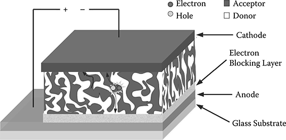
FIGURE 3.1
Configuration of organic photovoltaic cells made from BHJs.
3.2 Fundamentals of Organic Photovoltaic Cells
In this section, we briefly introduce the fundamentals of organic photovoltaic cells. More details on device physics can be found in the review article by Deibel et al. [7].
After light absorption, tightly bound electron-hole pairs (excitons) are created in organic semiconductors because of their low dielectric constants. In order to convert the solar energy into electricity, excitons must be separated into free carriers (electrons and holes) before they decay to ground states. The most efficient way for exciton dissociation is through a BHJ configuration (Figure 3.1) in which the electron donor and acceptor materials are blended into an intimately mixed nanostructure with the characteristic phase separation length scale of the order of 10-20 nm. Because the size of the phase-separated domains in the blend is similar to the exciton diffusion length, exciton decay can be significantly reduced because of the sufficient interfaces in the proximity of every generated exciton. For a polymer BHJ configuration with proper nanoscale morphology, the exciton dissociation is so sufficient that the exciton dissociation efficiency is close to 100% [8]. The disadvantage of a BHJ configuration is that it requires percolated pathways for the charge carriers transporting to their corresponding electrodes. Even though there are other kinds of configurations for organic photovoltaic cells, such as bilayer, we mainly discuss the BHJ configuration because of its obviously better performance. By default, in this chapter organic photovoltaic cells are referred to as those with a BHJ configuration.
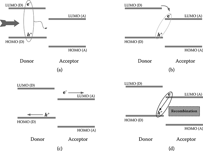
FIGURE 3.2
Schematic diagram to show the basic working principle of organic photovoltaic cells: (a) exciton formation and diffusion; (b) exciton dissociation; (c) free carrier transport; (d) geminate recombination.
The complete operation process of organic photovoltaic cells can be summarized as follows: the incident light is absorbed in the active layer, and tightly bounded excitons (electron-hole pair) are generated (Figure 3.2a); the excitons then diffuse to the D-A interface and dissociate into charge-transfer excitons (polarons) [9], which can be further separated into free electrons and holes (Figure 3.2b). Subsequently, these free charge carriers are then transported to and finally collected by the corresponding electrodes, respectively (Figure 3.2c); During the exciton diffusion and charge carrier transport processes, recombination losses will occur. The excitons may decay to ground states before they reach the D-A interface (not shown); the charge transfer states may also undergo geminate recombination (Figure 3.2d). The charge carriers could be further lost during transport through either mono-molecular or bimolecular recombination (not shown in the figure).
The power conversion efficiency of any photovoltaic cells can be obtained from their current-voltage (J-V) characteristics under standard illumination. The typical J−V curves of a photovoltaic device under illumination (solid line) are simulated as shown in Figure 3.3. The open circuit voltage Voc is the maximum voltage that can be generated in the cell, and corresponds to the voltage where current under illumination is zero. The current density that can run through the cell at zero applied voltage is called the short circuit current JSC. The maximum electrical power Pmax of a photovoltaic cell is located in the fourth quadrant where the product of current density J and voltage V reaches its maximum value. The ratio between Pmax and Voc × JSC represents the quality of the J−V curve shape and is defined as the fill factor (FF)
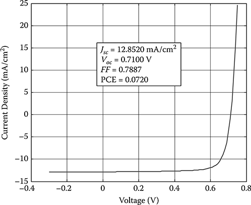
FIGURE 3.3
J-V characteristic curves of the typical PV device under illumination.
The power conversion efficiency is a common parameter to characterize the overall performance of a solar cell, but it is not convenient to analyze the device performance in detail, especially for organic photovoltaic cells with BHJ. External quantum efficiency (ηEQE), defined as the ratio of the number of charge carriers collected by the solar cell to the number of photons at a given energy shining on the solar cell from outside (incident photons), is another common parameter to characterize the performance of a solar cell responding to light at a certain wavelength, which has been frequently used to analyze the device performance. The external quantum efficiency of organic photovoltaic cells can be expressed by the product of the efficiencies of four sequential steps through the following formula [10]:
where ηA represents the efficiency of photon absorption leading to the generation of excitons; ηED represents the efficiency of exciton diffusion to the D−A interface; ηda represents the efficiency of exciton dissociation at the D−A interface; ηCT represents the efficiency of free charge transport to the electrodes; and ηCC represents the efficiency of the charge collection at the electrodes. Frequently, we use the following formula to calculate external quantum efficiency of any solar cells for simplicity:
where ηG is the free carrier generation efficiency with ηG = ηED ηda and ηC is the free carrier collection efficiency with ηC = ηCT*TCC. Another important parameter to characterize the performance of solar cells is the internal quantum efficiency (ηIQE), defined as the ratio of the number of charge carriers collected by the solar cell to the number of photons absorbed by the active layer, which can be calculated by ηiqe = ηG * ηC.
3.3 Optical Modeling
The purpose of optical modeling is to calculate the light absorption and exciton creation based on materials properties and the structure of organic photovoltaic cells. In this section, we first introduce the solar spectrum, and then describe the calculation of light absorption for homogeneous layers by the optical transfer matrix theory.
The surface temperature of the sun is around 5800 K, so the radiation spectrum from the sun is similar to the blackbody radiation at 5800 K. The radiation power density of the sun on the external atmosphere of the Earth (without considering absorption of the Earth's atmosphere) is
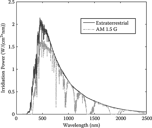
FIGURE 3.4
Solar spectrum. The solid curve is extraterrestrial measurement data and the dotted curve represents AM 1.5G spectrum. (Original data from http://rredc.nrel.gov/solar/spectra/.)
where rs is radius of the sun, rs = 6.96*108 m; and dSE is the distance between the sun and the Earth, dSE = 1.496*1011 m. For the characterization of ordinary solar cells on the Earth, the incident spectrum AM 1.5 global is used because the Earth's atmosphere absorbs incident light with a certain wavelength, which results in the deviation of the solar spectrum on the Earth from 5800 K blackbody radiation. In the following discussion, we use the AM 1.5 global spectrum (dotted curve; certified by the National Renewable Energy Laboratory), in which there are some distinct features corresponding to the specific absorption of the Earth's atmosphere.
Traditionally, the Beer-Lambert law is often used to describe the light intensity in bulk materials, assuming an exponential decay as
where I(x) is the light intensity at position x, I0 is the incident light intensity, and α is the absorption coefficient. However, light absorption in organic
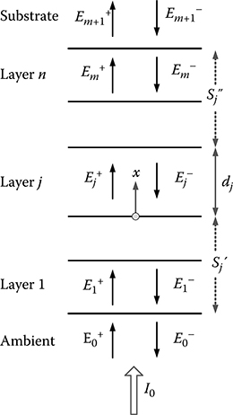
FIGURE 3.5
Schematic of m-layer structure between ambient and substrate.
photovoltaic cells is greatly affected by optical interference given that the thickness of each layer is less than the light wavelength. Figure 3.5 shows optical transport in a typical multilayer solar cell. A plane wave is incident from the left at an m-layer structure (layer 1 to layer m) between a semi-infinite transparent ambient and a semi-infinite opaque substrate. Due to the interference effect in the thin-film device, the optical electric field at any point x in layer j is a complex quantity and consists of a positive component and a negative component . The optical properties of each layer (j) are described by the thickness dj. and the complex index of refraction as
Since the thickness of thin films in organic photovoltaic cells is generally less than the wavelength of incident light, the optical effects such as reflections and interference are important and cannot be neglected when evaluating the electromagnetic field inside the device. The behavior of the light in the devices or the electromagnetic field distribution can be calculated either from an optical transfer matrix or from Maxwell equations. Optical transfer matrix theory is an approach to model the light propagation through a one-dimensional layered stack of different materials. To apply optical transfer matrix theory in the simulation of optical absorption and light intensity distribution within organic thin film solar cell, several assumptions need to be made [11]:
Layers included in the device are considered to be homogeneous and isotropic, so that their linear optical response can be described by a scalar complex index of refraction.
Interfaces are parallel and flat compared to the wavelength of the light.
The incident light at the device can be described by plane waves.
For most organic photovoltaic cells without texturing on each layer, these conditions hold. Based on optical transfer matrix theory, the light behavior at the interface between j and k = j + 1 layers can be described by a 2 × 2 interface matrix containing the complex Fresnel coefficients. The interface matrix Ijk can be expressed as
The light propagating in layer j can be described by the layer matrix Lj as
where kj. = 2πñj/λ. From Lj- in Equation 3.8, the real part of complex refraction, nj, responses for the phase propagation and image part, κj, are related to the light absorption. The optical electric field in the ambient (subscript 0) is related to that in the substrate (subscript m + 1) by the total transfer matrix S,
where the total optical transfer matrix S is the product of all interface and layer matrices expressed as
The optical electric field at a distance x within layer j can be expressed as
To express Ej(x) in terms of known quantities, Equation 3.11 is split into two partial transfer matrices and . As illustrated in Figure 3.5, . These two matrices can be expressed as
For the partial system transfer matrices for layer j, we have:
where and refer to the left boundary (j − 1)j in layer j and and refer to the right boundary j(j + 1) in layer j. After algebraic manipulation, Equation 3.11 can be expressed as
where is the electric field of the incident light from the ambient, where
For a detailed derivation, please refer to [11]. After determining the distribution of optical electric field Ej (x) in layer j as Equation 3.16, the light intensity at a distance x within layer j of the device can be expressed as
where I0(λ) is the intensity of the incident light, is the internal intensity transmittance, and and are the absolute value and the argument of the complex reflection coefficient. The first term inside the brackets of Equation 3.19 on the right-hand side originates from the optical electric field propagating in the positive x direction , the second term from the field propagating in the negative x direction , and the third term arises from the optical interference of the first two terms. The third term becomes especially important when the thickness of thin film is comparable with the light wavelength. When the thickness of an active layer is much larger than the light wavelength (dj >> X), the third term is negligible, and only the first two terms dominate, converging to the Beer-Lambert law for bulk materials.
Once the distribution of light intensity in the active layer is determined, the rate of energy dissipated per unit volume Q can be determined as
where α(λ) = 2πκ/λ is the absorption coefficient of the active layer. Then the density of photon absorbed in the active layer is
where h is Planck's constant, and c is light speed in a vacuum.
The photon absorption versus the thickness of the active layer for the AM 1.5G spectrum is shown in Figure 3.6. It can be seen that an optical interference effect exists if the optical transfer matrix method (solid curve) is applied and as a result, the absorption is enhanced at a certain thickness. The calculation results from the Beer-Lambert law (dashed curve); however, it shows no sign of oscillation. The simulation results based on the optical transfer matrix indicate that the optimal thickness of the active layer is approximately either 90 nm or 220 nm, coincident with experimental observations [12,13].
3.4 Electrical Modeling and Simulation by Drift-Diffusion Model
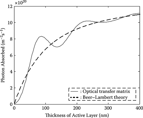
FIGURE 3.6
Calculated photons absorbed of AM 1.5G spectrum in the P3HT/PCBM solar cell versus its thickness.
The full current-voltage (J−V) characteristics of organic photovoltaic cells can be simulated by an equivalent-circuit model. Considering that such a model hardly reveals any fundamental physics of the devices, it is not discussed. Instead, we review how to simulate full current–voltage (J−V) characteristics of organic photovoltaic cells by the continuum drift-diffusion model, which reveals more physics of the organic photovoltaic cells. The drift-diffusion model is derived from Poisson's equation and continuity equations for electrons and holes, which are commonly used for describing the electrical behavior of semiconductor devices:
where Φ represents the electric potential; q is the unit charge; ɛ is the dielectric constant of the semiconductor; n and p are the electron and hole density, respectively; Jn, p is the electron (hole) current; G is the generation rate; and Rn(p) is the recombination rate. Equation 3.22 is the Poisson equation and Equations 3.23 and 3.24 are the continuity equations. The full J−V characteristics of organic photovoltaic cells can be obtained by solving these equations when the mean effects of the band gap and bulk mobility are considered.
For steady-state analysis (∂n/∂t = ∂p/∂t = 0), Equations 3.23 and 3.24 can be simplified as
Jn (Jp) can be written as functions of Φ, n and p, consisting of drift and diffusion components:
where μn(p) is the electron (hole) mobility and Dn(p) is the electron (hole) diffusion coefficient. By taking Equations 3.27 and 3.28 back to Equations 3.25 and 3.26, we can have the two following carrier continuity equations:
The goal of the simulation is to calculate carrier density n(x), p(x) as well as electric potential Φ(x) and then obtain the current with respect to the externally applied voltage (J−V characteristics). To simulate organic photovoltaic cells using the above model, several critical issues need to be clarified considering the unique properties of BHJ.
Permittivity: The permittivity ɛ is a spatially averaged dielectric constant of donor/acceptor blend, and hence ɛ is different for blends with different weight ratios between donor and acceptor materials [14].
Mobility: The bulk carrier (or apparent) mobility (μe for electrons and μh for holes) in the BHJ configuration, dependent on the nanoscale morphology in the disordered blend, is different from the value in its pure phase [15]. In addition to the dependence on nanoscale morphology and disorder, the apparent mobility is also largely dependent on the electrical field and free carrier concentration [16]. The apparent mobility further affects other aspects of the device such as recombination, short-circuit current, and open-circuit voltage, and thus the device performance [17] Fortunately, the dependence on electrical field and carrier concentration is considered as weak at low electrical fields (less than 107 V/m) and low carrier concentration [16] Therefore, it is usually safe to assume a constant mobility from short-circuit to open-circuit ranges.
Open Circuit Voltage: Open-circuit voltage is limited by the polaron pair energy [18,19] and also weakly affected by the work functions of the electrodes [20]. Therefore, it is not difficult to estimate the exact open-circuit voltage In the simulation, the common approach to estimate the Voc is taking an offset from the effective bandgap, expressed as Voc = LUMOa - HOMOd-Δ [21].
Einstein Relation: Traditionally, the classic Einstein relation (Dn,p/μn,p = kT/q) is assumed. However, deviation from the Einstein relation in disordered semiconductors has been reported [22-24]. A generalized Einstein relation can be used for disordered organic materials with modifications that the LUMO energy level is from the acceptor and the HOMO energy level is from the donor [25].
Boundary Conditions: Dirichlet boundary conditions [12,21] with ohmic contacts are assumed, where the surface potential and carrier concentrations are fixed at both ends.
Recombination: The determination of dominant loss mechanism in organic photovoltaic cells is very critical to correctly model and simulate their operation Unfortunately, the exact mechanism of the recombination is not clear yet It is commonly accepted that the recombination in organic photovoltaic cells is not a Langevin-type bimolecular recombination, but its true mechanism is still under heated debate. The majority believe bimolecular recombination is dominant, even though it has been suppressed compared to a Langevin-type recombination The reduced bimolecular recombination is supported not only by direct experimental studies [26–29] but also by deviation of the ideality factor [30] and by fitting simulation to light-intensity dependent J–V characteristics [31]. Recently, several researchers, including the authors, have suggested that monomolecular recombination may dominate in polymer BHJ solar cells [32–34] This argument is supported by studying the light-intensity dependent J–V characteristics for regions below the open-circuit condition. To reconcile the two contradictory opinions (either monomolecular or bimolecular), Cowan et al. proposed that the recombination loss is voltage dependent and evolves from monomolecular recombination at the short-circuit condition to bimolecular recombination at the open-circuit condition [35], which sounds more reasonable.
TABLE 3.1 Parameter Normalization
Source: L. Liu, and G. Li, "Modeling and simulation of organic solar cells," in IEEE Nanotechnology Materials and Devices Conference, Monterey, California, 2010.
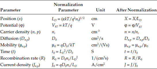
Because of the coupling between the electric potential φ and carrier density n(p) in the drift current, it is impractical to solve differential equations (3.22-3.26) analytically. Therefore, a numerical method must be used to solve coupled differential equations. The first step is parameter normalization, which simplifies the calculation in the numerical simulation, especially for Poisson and continuity equations in which there are some constant parameters. The normalized parameters include Debye length, intrinsic carrier density (ni), thermal energy (kT/q), and others, as shown in Table 3.1.
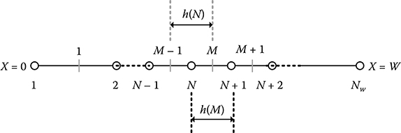
FIGURE 3.7
Schematic of one-dimensional discretization.
After normalization, the second step is to discretize the electric potential φ and carrier density n(p) on a simulation grid so that the continuous functions can be represented by vectors of function values at the nodes, and the differential operator is replaced by suitable difference operators A one-dimensional ununiformed grid is shown in Figure 3.7. The region considered here (x = 0 to x = W) has been discretized to Nw nodes, which were numbered as 1, 2, ..., N, ..., Nw. The middle point between the N node and N + 1 node was named M. Therefore, there are totally Nw − 1 middle points between the nearest nodes, named 1, 2, ..., M, ..., Mw (Mw = Nw − 1). The distance between the N node and N + 1 node is h(M), and the distance between the middle point M − 1 and M is h(N). The discretization of electric potential 9 using the central differential formula can be expressed as
The discretization of carrier density n(p) requires more care because the change of electric potential ϕ in the semiconductor is gradual, but the change of carrier density n(p) is rapid, and hence the general calculation method will always result in a nonconverge situation. Therefore, the Scharfetter-Gummel method was applied to discretize the carrier density n as [37]
where the pre-factor gi(x) is
It is clear that in the middle between the nearest grid points, the carrier density has a nonlinear relation with distance x and the continuity equations are coupled together. In addition, the change of electric potential in the semiconductor is gradual, but the change of carrier density is very rapid, and hence the general calculation method will not always converge. After discretization of Φ and n (p) by the central difference formula and by the Scharfetter and Gummel method [37], respectively, either a decoupled iteration method [38] (Gummel's method) or a coupled method [39] (Newton method) can be employed to solve the linearized and discretized differential equations. A detailed description regarding discretization and linearization, as well as Gummel's method and the Newton method, can be found in Reference 40.
With these simulation algorithms, we can develop a simulation tool that is able to simulate the complete (J−V) characteristics of organic photovoltaic cells by considering the optical absorption under standard illumination as shown in Figure 3.3. With this simulation, we can also study the device physics of organic photovoltaic cells.
3.4 Electrical Modeling and Simulation by Monte Carlo Model
The nanoscale morphology of disordered bulk heterojunctions plays a critical role in determining overall device performance. It has been found that carrier mobility can be improved by ameliorating the nanoscale morphology of the active layer through thermal annealing [1,41−43] and solvent annealing [2,43,44] to improve the crystallinity and phase separation, which have been proven with XRD (x-ray diffraction) and TEM (transmission electron microscopy) [1]. Unfortunately, macroscopic simulation using the drift-diffusion model to derive Poisson's equation and continuity equations [5−8] only considers the mean effect of many factors without correlating the device performance to the nanomorphology. Mesoscopic approaches, such as Monte Carlo simulation, on the other hand, can help gain a deeper understanding of the relationship between the nanoscale morphology of the active layer and the performance of the device.
In order to study the relationship between the morphology and the performance of organic photovoltaic cells, a series of blend morphologies with different phase separations needs to be generated. In a P3HT:PCBM system with a weight ratio of 1:1, the scales of phase separation are characterized by domain size a = 3V/A, where V is the total active layer volume, and A is donor/acceptor interfacial area. Herein, the Ising model [45] is often adopted to obtain the nanoscale morphology. The morphology generation process is shown as follows:
First, the active layer is discretized into many small cubes (a lattice constant of 1 nm is used here). Every lattice, also called a site, is assigned a value 0 or 1 with equal probability, where 0 stands for donor and 1 for acceptor.
Second, choose two neighboring sites randomly from all the lattices and calculate the Ising Hamiltonian value of the system comprised of the chosen two sites, their neighbors, and second-nearest neighbors according to the following equation:
where δsi,sj is the delta function and J = +1. 0 KbT. Here, Kb represents the Boltzmann constant and T is the temperature. The contribution of the second-nearest neighbors is scaled by a factor of 1/√2.
Third, exchange the spin value (0 or 1) of the chosen two sites with the probability
where Δɛ is the difference between Hamiltonian values before and after exchange.
Finally, after a great number of attempted spin exchanges, a morphology series with the required domain sizes can be generated as shown in Figure 3.8a and 3.8b.
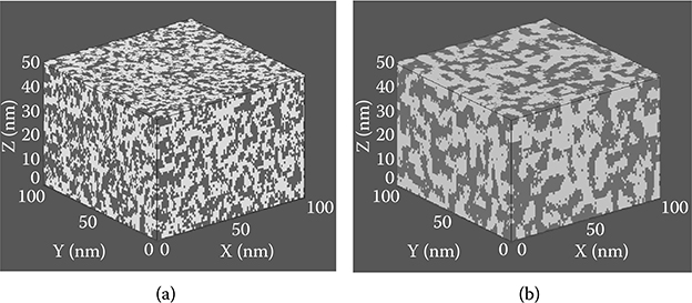
FIGURE 3.8
Morphologies generated by the Ising model for P3HT:PCBM devices: nanoscale morphology of BHJs with weight ratio of 1:1 and with different phase separations at (a) 5 nm and (b) 10 nm.
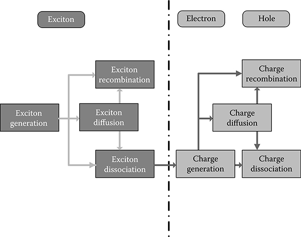
FIGURE 3.9
The major events during the operation process of organic photovoltaic solar cells.
Three kinds of particles (exciton, electron, and hole) are included in the model of polymer BHJ solar cells. Careful analysis of the mechanism of photo-current generation will result in ten types of events as shown in Figure 3.9.
The most important parameters to be set are the attempt-to-happen rates of all the events considered. The values of these constants for the P3HT:PCBM system used in the simulation are listed in Table 3.2. They are obtained based on either experienced values from experiments or on theoretical calculations, specifically:
TABLE 3.2 Event Happen Rate Constants
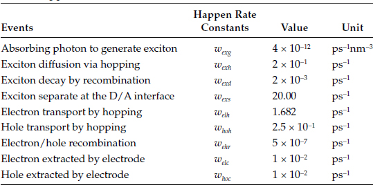
Source: Data from M. Casalegno, G. Raos, and R. Po, "Methodological assessment of kinetic Monte Carlo simulations of organic photovoltaic devices: The treatment of electrostatic interactions," Journal of Chemical Physics, vol. 132, no. 9, p. 094705, 2010.
wexg, wehr, welc and whoc are experienced values chosen according to experiments.
Wexh = 6Dex/L2 (Brownian motion model) where Dex is the diffusion coefficient, which is calculated according to the Einstein relationship; L is the average hopping length, which is equal to the length of smallest lattice side l = 1 nm, since only the hopping between the nearest neighbors is considered.
wexd is equal to 1/τ, where τ is the lifetime of the exciton.
wexs is set to be the inverse of the exciton dissociation time at the D/A interface, while 0 at other sites.
wdh{hoh) can be calculated by combining the Brownian motion model and the Einstein relationship as
where μ is the mobility, e is the unit charge, and γ is the localization constant valued at 2.0 nm−1.
The relative permittivity of the active layer is set to be a spatial mean value.
Figure 3.10a shows the simulation results that excitons were generated at random sites, then the dissociation of excitons, and the hopping of the generated electrons (dark) and holes (gray). The influence of morphology in the blend on exciton dissociation efficiency is shown in Figure 3.10b. It can be seen that smaller domain size yields higher exciton dissociation efficiency.
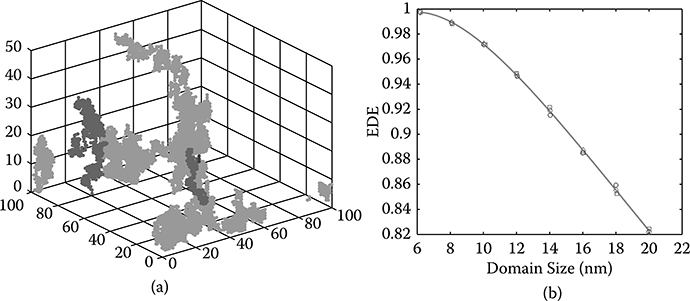
FIGURE 3.10
Simulation of exciton and charge carriers in BHJ blends with phase-separation size 5 nm (a) and simulation of exciton dissociation efficiency for BHJ blend with phase-separation size 5 nm (b).
Monte Carlo models can effectively account for the phase-separated morphology [47], but they mainly focus on one or a few aspects of the device. Even though Monte Carlo is capable of simulating a few points of the J−V characteristics [48], it is not convenient to simulate the full experimental J−V characteristics. Even though the results from Monte Carlo simulation now meet our expectations from our understanding of polymer BHJ, their validity and accuracy need to be further investigated considering the following limitations: (1) the morphology generated by the Ising model hardly resembles the real morphology of a device, which is much more complex; (2) there is a lack of effective tools to characterize the nanoscale morphology and thus to validate the results from Monte Carlo simulation through experiments; and (3) we have limited understanding of the working principles of polymer BHJ. Because Monte Carlo simulation is fundamentally a statistical approach, its accuracy also is dependent on the sample size used in the calculation. A larger sample size will increase the accuracy but may require unaffordable computational time. Therefore, the validity and accuracy need to be much improved in future research.
3.5 Discussion and Conclusion
In this chapter, we first provide background on the fundamentals of organic photovoltaic cells from basic configurations and operations to device performance, as well as the nanoscale morphology that dictates the performance of the device. We then introduce optical modeling for calculation of light absorption based on transfer matrix theory that accounts for the reflection and interference in each layer. We further present electrical modeling for simulating device performance. Two kinds of electrical modeling approaches are discussed: the macroscopic approach using the drift-diffusion model and the mesoscopic approach using a Monte Carlo model. The macroscopic approach based on the drift-diffusion model can predict the overall performance of organic photovoltaic cells by taking into account the mean effects of the devices, but it fails to take nanoscale morphology into account in the model. The mesoscopic approach using the Monte Carlo model does take nanoscale morphology into consideration but it can study only one or a few aspects of organic photovoltaic cells.
We have shown that modeling and simulation of organic photovoltaic cells are very useful in predicting device performance and analyzing working principles. However, the results from modeling and simulation are only meaningful when the modeling and simulation have been proven to be valid and accurate. Valid modeling and simulation have to be built on the correct understanding of the working principles of devices as well as experimental verification. Some of the working mechanisms of organic photovoltaic cells such as recombination are not completely clear; further validation of some modeling and simulation approaches such as Monte Carlo simulation is necessary. The accuracy of modeling and simulation is based on the accuracy of the feed-in parameters. Unfortunately, there is still a lack of effective tools to measure some critical parameters such as nanoscale morphology, energy disorder, and recombination. Therefore, the validation and accuracy of modeling and simulation are the major limiting factors that preclude their wide usage.
To make organic photovoltaic cells commercially viable, there is a pressing need to study modeling and simulation, and thus to optimize organic photovoltaic cells for the best device performance. So far, neither the macroscopic approach based on the drift-diffusion model nor the mesoscopic approach based on Monte Carlo modeling alone is able to exactly describe the full operation of organic BHJ solar cells. The macroscopic approach can simulate the macroscopic performance of the device by considering the mean effect of many factors without directly correlating device performance to nanomorphology. Mesoscopic simulation based on the Monte Carlo model takes nanoscale morphology into consideration to simulate a few important factors such as exciton dissociation, but it fails to simulate the macroscopic performance of the devices because of the requirement for excessive computational power.
Because of the complexity of organic photovoltaic cells, it is not possible to simply tune one or a few parameters to achieve optimal performance. Instead, the optimization of organic photovoltaic cells is a fine balancing act, which means all the parameters need to be tuned simultaneously. Therefore, a multiscale modeling and simulation approach that includes all the aspects of organic photovoltaic cells in the model is needed. For example, Monte Carlo simulation can be used to predict a few properties of BHJs such as exciton dissociation, carrier recombination, and carrier bulk mobility with respect to nanoscale morphology; then these parameters can be fed into a macroscopic simulation based on the drift-diffusion model, which can predict the overall performance of a device. By combining the optical model with these multiscale simulations, the optimal design of the devices such as the thickness of the functional layer and the nanoscale morphology of the BHJs can be identified simultaneously. The optimization of organic photovoltaic cells via multiscale modeling and simulation is discussed in Chapter 4.
References
1. W. L. Ma, C. Y. Yang, X. Gong, K. Lee, and A. J. Heeger, "Thermally stable, efficient polymer solar cells with nanoscale control of the interpenetrating network morphology," Advanced Functional Materials, vol. 15, no. 10, pp. 1617-1622, 2005.
2. G. Li, V. Shrotriya, J. Huang, Y. Yao, T. Moriarty, K. Emery, and Y. Yang, "High-efficiency solution processable polymer photovoltaic cells by self-organization of polymer blends," Nature Materials, vol. 4, no. 11, pp. 864-868, 2005.
3. http://www.ecnmag.com/news/2011/12/Heliatek-Organic-Solar-Cells-Achieve-Record-Efficiency/.
4. B. A. Gregg, and M. C. Hanna, "Comparing organic to inorganic photovoltaic cells: Theory, experiment, and simulation," Journal of Applied Physics, vol. 93, no. 6, pp. 3605-3614, 2003.
5. J. J. M. Halls, C. A. Walsh, N. C. Greenham, E. A. Marseglia, R. H. Friend, S. C. Moratti, and A. B. Holmes, "Efficient photodiodes from interpenetrating polymer networks," Nature, vol. 376, no. 6540, pp. 498-500, 1995.
6. G. Yu, J. Gao, J. C. Hummelen, F. Wudl, and A. J. Heeger, "Polymer photovoltaic cells: Enhanced efficiencies via a network of internal donor-acceptor heterojunctions," Science, vol. 270, no. 5243, pp. 1789-1791, 1995.
7. D. Carsten, and D. Vladimir, "Polymer-fullerene bulk heterojunction solar cells," Reports on Progress in Physics, vol. 73, no. 9, p. 096401, 2010.
8. C. J. Brabec, N. S. Sariciftci, and J. C. Hummelen, "Plastic solar cells," Advanced Functional Materials, vol. 11, no. 1, pp. 15-26, 2001.
9. T. M. Clarke, and J. R. Durrant, "Charge photogeneration in organic solar cells," Chemical Reviews, vol. 110, pp. 6736-6767, 2010.
10. X. Zhao, B. Mi, Z. Gao, and W. Huang, "Recent progress in the numerical modeling for organic thin film solar cells," Science China Physics, Mechanics and Astronomy, vol. 54, no. 3, pp. 375-387, 2011.
11. L. A. A. Pettersson, L. S. Roman, and O. Inganas, "Modeling photocurrent action spectra of photovoltaic devices based on organic thin films," Journal of Applied Physics, vol. 86, no. 1, pp. 487–496, 1999.
12. D. W. Sievers, V. Shrotriya, and Y. Yang, "Modeling optical effects and thickness dependent current in polymer bulk-heterojunction solar cells," Journal of-Applied Physics, vol. 100, no. 11, pp. 114509-7, 2006.
13. R. Hausermann, E. Knapp, M. Moos, N. A. Reinke, T. Flatz, and B. Ruhstaller, "Coupled optoelectronic simulation of organic bulk-heterojunction solar cells: Parameter extraction and sensitivity analysis," Journal of Applied Physics, vol. 106, no. 10, pp. 104507–9, 2009.
14. V. D. Mihailetchi, L. J. A. Koster, J. C. Hummelen, and P. W. M. Blom, "Photocurrent generation in polymer-fullerene bulk heterojunctions," Physical Review Letters, vol. 93, no. 21, p. 216601, 2004.
15. X. N. Yang, J. Loos, S. C. Veenstra, W. J. H. Verhees, M. M. Wienk, J. M. Kroon, M. A. J. Michels, and R. A. J. Janssen, "Nanoscale morphology of high-performance polymer solar cells," Nano Letters, vol. 5, no. 4, pp. 579–583, 2005.
16. L. J. A. Koster, "Charge carrier mobility in disordered organic blends for photo-voltaics," Physical Review B, vol. 81, no. 20, p. 205318, 2010.
17. F. Xu, and D. Yan, "The role of mobility in bulk heterojunction solar cells," Applied Physics Letters, vol. 99, no. 11, p. 113303, 2011.
18. A. Cravino, "Origin of the open circuit voltage of donor-acceptor solar cells: Do polaronic energy levels play a role?," Applied Physics Letters, vol. 91, no. 24, p. 243502, 2007.
19. K. Vandewal, K. Tvingstedt, A. Gadisa, O. Inganas, and J. V. Manca, "On the origin of the open-circuit voltage of polymer-fullerene solar cells," Nature Material, vol. 8, no. 11, pp. 904–909, 2009.
20. C. J. Brabec, A. Cravino, D. Meissner, N. S. Sariciftci, T. Fromherz, M. T. Rispens, L. Sanchez, and J. C. Hummelen, "Origin of the open circuit voltage of plastic solar cells," Advanced Functional Materials, vol. 11, no. 5, pp. 374-380, 2001.
21. L. J. A. Koster, E. C. P. Smits, V. D. Mihailetchi, and P. W. M. Blom, "Device model for the operation of polymer/fullerene bulk heterojunction solar cells," Physical Review B, vol. 72, no. 8, p. 085205, 2005.
22. Q. Gu, E. A. Schiff, S. Grebner, F. Wang, and R. Schwarz, "Non-Gaussian Transport Measurements and the Einstein Relation in Amorphous Silicon," Physical Review Letters, vol. 76, no. 17, p. 3196, 1996.
23. Y. Roichman, and N. Tessler, "Generalized Einstein relation for disordered semiconductors—implications for device performance," Applied Physics Letters, vol. 80, no. 11, pp. 1948–1950, 2002.
24. H. J. Snaith, L. Schmidt-Mende, M. Gratzel, and M. Chiesa, "Light intensity, temperature, and thickness dependence of the open-circuit voltage in solid-state dye-sensitized solar cells," Physical Review B, vol. 74, no. 4, p. 045306, 2006.
25. R. Yohai, and T. Nir, "Generalized Einstein relation for disordered semiconductors—implications for device performance," Applied Physics Letters, vol. 80, no. 11, pp. 1948–1950, 2002.
26. G. Juska, K. Genevicius, N. Nekrasas, G. Sliauzys, and R. Osterbacka, "Two dimensional Langevin recombination in regioregular poly(3-hexylthiophene)," Applied Physics Letters, vol. 95, no. 1, p. 013303, 2009.
27. G. Juska, K. Genevicius, N. Nekrasas, and G. Sliauzys, "Two-dimensional Langevin recombination," Physica Status Solidi (c), vol. 7, no. 3–4, pp. 980–983, 2010.
28. C. Deibel, A. Baumann, and V. Dyakonov, "Polaron recombination in pristine and annealed bulk heterojunction solar cells," Applied Physics Letters, vol. 93, no. 16, pp. 163303–3, 2008.
29. G. JuŠka, K. Genevicius, N. NekraŠas, G. SliauŽys, and G. Dennler, "Trimolecular recombination in polythiophene: fullerene bulk heterojunction solar cells," Applied Physics Letters, vol. 93, no. 14, p. 143303, 2008.
30. G. A. H. Wetzelaer, M. Kuik, M. Lenes, and P. W. M. Blom, "Origin of the dark-current ideality factor in polymer:fullerene bulk heterojunction solar cells," Applied Physics Letters, vol. 99, no. 15, p. 153506, 2011.
31. C. G. Shuttle, R. Hamilton, B. C. O'Regan, J. Nelson, and J. R. Durrant, "Charge-density-based analysis of the current-voltage response of polythiophene/fullerene photovoltaic devices," Proceedings of the National Academy of Sciences USA, vol. 107, no. 38, pp. 16448–16452, 2010.
32. C. R. McNeill, S. Westenhoff, C. Groves, R. H. Friend, and N. C. Greenham, "Influence of Nanoscale Phase Separation on the Charge Generation Dynamics and Photovoltaic Performance of Conjugated Polymer Blends: Balancing Charge Generation and Separation," Journal of Physical Chemistry C, vol. 111, no. 51, pp. 19153–19160, 2007.
33. R. A. Street, M. Schoendorf, A. Roy, and J. H. Lee, "Interface state recombination in organic solar cells," Physical Review B, vol. 81, no. 20, p. 205307, 2010.
34. L. Liu, and G. Li, "Investigation of recombination loss in organic solar cells by simulating intensity-dependent current-voltage measurement," Solar Energy Materials and Solar Cells, vol. 95, no. 9, pp. 2557–2563, 2011.
35. S. R. Cowan, A. Roy, and A. J. Heeger, "Recombination in polymer-fullerene bulk heterojunction solar cells," Physical Review B, vol. 82, no. 24, p. 245207, 2010.
36. L. Liu, and G. Li, "Modeling and simulation of organic solar cells," in IEEE Nanotechnology Materials and Devices Conference, Monterey, California, 2010.
37. D. L. Scharfetter, and H. K. Gummel, "Large-signal analysis of a silicon Read diode oscillator," IEEE Transactions on Electron Devices, vol. 16, no. 1, pp. 64–77, 1969.
38. H. K. Gummel, "A self-consistent iterative scheme for one-dimensional steady state transistor calculations," IEEE Transactions on Electron Devices, vol. 11, no. 10, pp. 455–465, 1964.
39. A. M. Winslow, "Numerical solution of the quasilinear poisson equation in a nonuniform triangle mesh," Journal of Computational Physics, vol. 1, no. 2, pp. 149-172, 1966.
40. E. Knapp, R. Hausermann, H. U. Schwarzenbach, and B. Ruhstaller, "Numerical simulation of charge transport in disordered organic semiconductor devices," Journal of Applied Physics, p. 054504, 2010.
41. X. Yang, J. Loos, S. C. Veestra, W. J. H. Verhees, M. M. Wienk, J. M. Kroon, M. A. J. Michels, and R. A. J. Janssen, "Nanoscale morphology of high-performance polymer solar cells," Nano Letters, vol. 5, no. 4, pp. 579–583, 2005.
42. H. Hoppe, M. Niggemann, C. Winder, J. Kraut, R. Hiesgen, A. Hinsch, D. Meissner, and N. S. Sariciftci, "Nanoscale morphology of conjugated polymer/fullerene-based bulk-heterojunction solar cells," Advanced Functional Materials, vol. 14, no. 10, pp. 1005–1011, 2004.
43. Y. Zhao, Z. Xie, Y. Qu, Y. Geng, and L. Wang, "Solvent-vapor treatment induced performance enhancement of poly(3-hexylthiophene):methanofullerene bulk-heterojunction photovoltaic cells," Applied Physics Letters, vol. 90, no. 4, p. 043504, 2007.
44. S. Miller, G. Fanchini, Y.-Y. Lin, C. Li, C.-W. Chen, W.-F. Su, and M. Chhowalla, "Investigation of nanoscale morphological changes in organic photovoltaics during solvent vapor annealing," Journal of Materials Chemistry, vol. 18, no. 3, pp. 306-312, 2008.
45. S. G. Brush, "History of the Lenz-Ising model," Reviews of Modern Physics, vol. 39, no. 4, pp. 883-893, 1967.
46. M. Casalegno, G. Raos, and R. Po, "Methodological assessment of kinetic Monte Carlo simulations of organic photovoltaic devices: The treatment of electrostatic interactions," Journal of Chemical Physics, vol. 132, no. 9, p. 094705, 2010.
47. F. Yang, and S. R. Forrest, "Photocurrent generation in nanostructured organic solar cells," ACS Nano, vol. 2, no. 5, pp. 1022–1032, 2008.
48. R. A. Marsh, C. Groves, and N. C. Greenham, "A microscopic model for the behavior of nanostructured organic photovoltaic devices," Journal of Applied Physics, vol. 101, no. 8, p. 083509, 2007.