
3
The PIC Microcontroller
3.1 THE PIC MICROCONTROLLER FAMILY
The PIC microcontroller is a family of microcontrollers manufactured by the Microchip Technology Inc. Currently the PIC is one of the most popular microcontrollers used in education, and in commercial and industrial applications. The family consists of over 140 devices, ranging from simple 4-pin dual in-line devices with 0.5 K memory, to 80-pin complex devices with 32 K memory.
Even though the family consists of a large number of devices, all the devices have the same basic structure, offering the following fundamental features:
- reduced instruction set (RISC) with only 35 instructions;
- bidirectional digital I/O ports;
- RAM data memory;
- rewritable flash, or one-time programmable program memory;
- on-chip timer with pre-scaler;
- watchdog timer;
- power-on reset;
- external crystal operation;
- 25 mA current source/sink capability;
- power-saving sleep mode.
More complex devices offer the following additional features:
- analog input channels;
- analog comparators;
- serial USART;
- nonvolatile EEPROM memory;
- additional on-chip timers;
- external and internal (timer) interrupts;
- PWM output;
- CAN bus interface;
- I2Cbus interface;
- USB interface;
- LCD interface.
The PIC microcontroller product family currently consists of six groups:
- PIC10FXXX 12-bit program word;
- PIC12CXXX/PIC12FXXX 12/14-bit program memory;
- PIC16C5X 12-bit program word;
- PIC16CXXX/PIC16FXXX 14-bit program word;
- PIC17CXXX 16-bit program word;
- PIC18CXXX/PIC18FXXX 16-bit program word.
3.1.1 The 10FXXX Family
Table 3.1 gives a summary of the features of this family. PIC10F200 is a member of this family with the following features.
PIC10F200. This microcontroller is available in a 6-pin SOT-23 package (see Figure 3.1), or in 8-pin PDIP package (see Figure 3.2). The device has 33 instructions, 256× 12 word flash program memory, 16 bytes of RAM data memory, four I/O ports, and one 8-bit timer. Clocking is from a precision 4 MHz internal oscillator. Other members of the family have larger memories and also an internal comparator.
Table 3.1 Some PIC10FXXX family members
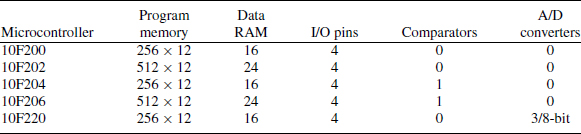

Figure 3.1 PIC10FXXX family in 6-pin SOT-23 package

Figure 3.2 PIC10FXXX family in 8-pin PDIP package
Table 3.2 Some PIC12CXXX family members Program

3.1.2 The 12CXXX/PIC12FXXX Family
Table 3.2 gives a summary of the features of this family. The PIC12C508 is a member of this family with the following features.
PIC12C508. This is another low-cost microcontroller available in an 8-pin dual in-line package. The device has 512× 12 word flash memory, 25 bytes of RAM data memory, six I/O ports, and one 8-bit timer. Operation is from a 4 MHz clock. Other members of the family have larger memories, higher speed, and A/D converters (e.g. 12C672).
The PIC12FXXX family has the same structure as the 12CXXX but with flash program memory and additional EEPROM data memory.
3.1.3 The 16C5X Family
Table 3.3 gives a summary of the features of this family. These devices have 14-, 18-, 20- and 28-pin packages. The PIC16C54 is a member of this family with the following features.
PIC16C54. This is an 18-pin microcontroller with 384× 12 EPROM program memory. The device has 25 bytes of RAM, 12 I/O port pins, a timer and a watchdog timer. Other members of the family have larger memories and more I/O ports.
3.1.4 The 16CXXX Family
Table 3.4 gives a summary of the features of this family. These devices are similar to the 16CXX series, but they have 14 bits of program memory and some of them have A/D converters. The PIC16C554 is a member of this family with the following features.
Table 3.3 Some PIC16C5X family members

Table 3.4 Some PIC16CXXX family members

PIC16C554. This is an 18-pin device with 512× 14 program memory. The data memory is 80 bytes and 13 I/O port pins are provided. Other members of this family provide A/D converters (e.g. PIC16C76), USART capability (e.g. PIC16C67), larger memory, more I/O port pins and higher speed.
The PIC16FXXX family (e.g. PIC16F74) is upward compatible with the PIC16CXXX family. These devices are also 14 bits wide and have flash program memory and an internal 4 MHz clock oscillator as added features.
3.1.5 The 17CXXX Family
These are 16-bit microcontrollers. The program memory capacity ranges from 8192 × 16 (e.g. PIC17C42) to 16 384× 16 (e.g. PIC17C766). The devices also have larger RAM data memories, higher current sink capabilities and larger I/O port pins, e.g. the PIC17C766 provides 66 I/O port pins. Table 3.5 gives a summary of the features of this family.
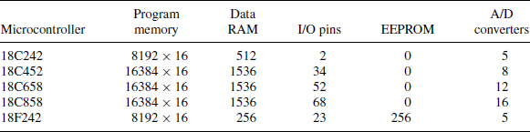
3.1.6 The PIC18CXXX Family
These are high-speed 16-bit microcontrollers, with maximum clock frequency 40 MHz. The devices in this family have large program and data memories, a large number of I/O pins, and A/D converters. They have an instruction set with 77 instructions, including multiplication. Table 3.6 gives a summary of the features of this family.
PIC18FXXX family members are upward compatible with PIC18CXXX. These microcontrollers in addition offer flash program memories and EEPROM data memories. Some members of the family provide up to 65 536× 16 program memories and 3840 bytes of RAM memory.
Table 3.5 Some PIC17CXXX family members Program
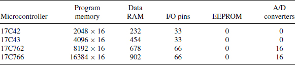
Table 3.6 Some PIC18CXXX family members
3.2 MINIMUM PIC CONFIGURATION
The minimum PIC configuration depends on the type of microcontroller used. Normally, the operation of a PIC microcontroller requires a power supply, reset circuit and oscillator.
The power supply is usually +5V and, as shown in Figure 3.3, can be obtained from the mains supply by using a step-down transformer, a rectifier circuit and a power regulator chip, such as the LM78L05.
Although PIC microcontrollers have built-in power-on reset circuits, it is useful in many applications to have external reset circuits. When the microcontroller is reset, all of its special function registers are put into a known state and execution of the user program starts from address 0 of the program memory.
As shown in Figure 3.4, reset is normally achieved by connecting a 4.7 K pull-up resistor from the master clear (MCLR) input to the supply voltage. Sometimes the voltage rises too slowly and the simple reset circuit may not work. In this case, the circuit shown in Figure 3.5 is recommended.
In many applications it may be required to reset the microcontroller by pressing an external button. The circuit given in Figure 3.6 enables the microcontroller to reset when the button is pressed.
PIC microcontrollers have built-in clock oscillator circuits. Additional components are needed to enable such clock oscillator circuits to function; some PIC microcontrollers have these built in, while others require external components. The internal oscillator can be operated in one of six modes:
- external oscillator;
- LP – low-power crystal;
- XT – low-speed crystal/resonator;
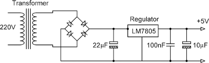
Figure 3.3 A simple microcontroller power source

Figure 3.4 Simple reset circuit

Figure 3.5 Recommended reset circuit
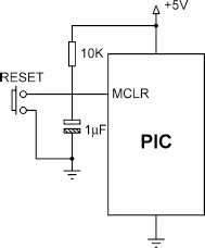
Figure 3.6 Push-button reset circuit
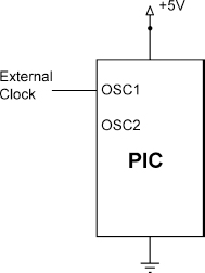
Figure 3.7 Using an external oscillator
- HS – high-speed crystal/resonator;
- RC – resistor and capacitor;
- no external components (only some PICs).
3.2.1 External Oscillator
An external oscillator can be connected to the OSC1 input as shown in Figure 3.7. The oscillator should generate square wave pulses at the required frequency. The timing accuracy depends upon the accuracy of this external oscillator. When operated in this mode, the chip should be programmed for LP, XT or HS clock mode.
3.2.2 Crystal Operation
An external crystal should be used when very accurate timing is required. As shown in Figure 3.8, the crystal should be connected between the OSC1 and OSC2 inputs together with a pair of capacitors. The value of the capacitors should be chosen as in Table 3.7. For example, with a crystal of 4 MHz, two 22 pF capacitors can be used.
3.2.3 Resonator Operation
Resonators are usually available in the frequency range of about 4–8 MHz. Although resonators are not as accurate as crystals, they are usually accurate enough for most applications. Resonators have the advantages that they are low-cost and only one component is required compared to three components in the case of crystals (the crystal itself and two capacitors). Figure 3.9 shows how a resonator can be used with PIC microcontrollers.

Table 3.7 Capacitor values for crystal operation


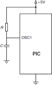
Figure 3.10 Using an RC circuit
3.2.4 RC Operation
There are many low-cost applications where the timing accuracy is not important – flashing an LED every second, scanning a keyboard, reading the temperature every second, etc. In such applications the clock pulses can be generated by using an external resistor and a capacitor. As shown in Figure 3.10, the resistor and the capacitor should be connected to the OSC1 input of the microcontroller.
The oscillator frequency depends upon the values of the resistor and the capacitor, the supply voltage and environmental factors, such as the temperature. Table 3.8 gives a list of typical resistor and capacitor values for most of the frequencies of interest. For example, a 5 K resistor and a 20 pF capacitor can be used to generate a clock frequency of about 4 MHz.
3.2.5 Internal Clock
Some PIC microcontrollers (e.g. PIC12C672) have built-in clock generation circuitry and do not require any external components to generate the clock pulses. The built-in oscillator is usually 4 MHz and can be selected during the programming of the devices. Figure 3.11 shows the circuit diagram of a minimum PIC microcontroller system using a 4 MHz resonator. A minimum PIC microcontroller system using a crystal is shown in Figure 3.12.
Table 3.8 Resistor and capacitor values C (pF)

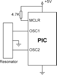
Figure 3.11 Resonator based minimum PIC microcontroller system

Figure 3.12 Crystal based minimum PIC microcontroller system
3.3 SOME POPULAR PIC MICROCONTROLLERS
In this section we shall look at the architectures of some of the popular PIC microcontrollers in greater detail. We have chosen the popular 18-pin PIC16F84 and the 40-pin PIC16F877 microcontrollers. The architectures and instruction sets of most of the other PIC microcontrollers are very similar, and with the knowledge gained here we should be able to use and program any other PIC microcontroller easily. Since our aim is to program the microcontrollers using a high-level language such as the C, there is no need to learn their exact architecture or assembly instruction set. We shall only look at the features which may be required while developing software using the C programming language.
3.3.1 PIC16F84 Microcontroller
The PIC16F84 is one of the most popular PIC microcontrollers used in many commercial, industrial and hobby applications. This is an 18-pin device which can operate at up to 20 MHz clock speed. It offers 1024× 14 flash program memory, 68 bytes of RAM data memory, 64 bytes of EEPROM nonvolatile data memory, 8-bit timer with pre-scaler, watchdog timer, 13 I/O pins, external and internal interrupt sources, and large current sink and source capability.
Figure 3.13 shows the pin configuration of the PIC16F84. The functions of various pins are as follows:
| RB0–RB7 | Bidirectional port B pins |
| RA0–RA4 | Bidirectional port A pins |
| Vdd | Supply voltage |
| Vss | Ground |
| OSC1 | Crystal, resonator, or external clock input |
| OSC2 | Crystal or resonator input |
| MCLR | Reset input |
| INT | External interrupt input (shared with RB0) |
| T0CK1 | Optional timer clock input (shared with RA3) |
Note that some pin names have a bar on them – for example, ![]() in Figure 3.13. This means that the pin will be active when the applied signal is at logic low (logic 0 in this case).
in Figure 3.13. This means that the pin will be active when the applied signal is at logic low (logic 0 in this case).
The PIC16F84 provides four external or internal interrupt sources:
- external interrupt on INT pin;
- timer overflow interrupt;
- state change interrupt on the four higher bits of port B (RB4–RB7);
- EEPROM memory data write complete interrupt.
The data RAM is also known as the register file map (RFM) and consists of 80 bytes. As shown in Figure 3.14, the RFM is divided into two parts: the special function registers (SFR), and the general purpose registers (GPR). The RFM is organized as two banks (more complex PIC microcontrollers may have more banks): bank 0 and bank 1. The bank of a register must be selected before a register in a bank can be read or written to. Some of the registers are common to both banks.

Figure 3.13 PIC16F84 pin configuration

Figure 3.14 Register file map of PIC16F84
The SFR are a collection of registers used by the CPU to control the internal operations and the peripherals – setting the I/O direction of a register, sending data to an I/O port, loading the timer register, etc. The SFR used while programming the microcontroller using a high-level language are described in the following sections.
3.3.1.1 OPTION REG Register
The OPTION_REG register is a readable and writable register at address 0 ×81 (hexadecimal) of the RFM. This register controls the timer pre-scaler, timer clock edge selection, timer clock source, external interrupt edge selection, and port B pull-up resistors. OPTION REG bit definitions are given in Figure 3.15. For example, to configure the external interrupt INT pin so that external interrupts are accepted on the falling edge of the INT input, the following bit pattern should be loaded into the OPTION_REG:
X0XXXXXX
where X is a don't-care bit and can be a 0 or a 1.
3.3.1.2 INTCON Register
This is the interrupt control register at addresses 0 ×0B and 0×8B of the RFM. The bit definitions of this register are shown in Figure 3.16. INTCON is used to enable/disable the various interrupt sources and interrupt flags. For an interrupt to be accepted by the CPU, the following conditions must be met:

Figure 3.15 OPTION_REG bit definitions

Figure 3.16 INTCON bit definitions
- The global interrupt flag in INTCON must be enabled (GIE = 1).
- The interrupt flag of the interrupting source in INTCON must be enabled (e.g. INTE=1 to enable INT external interrupts).
- Interrupt must physically occur (e.g. INT pin is raised to logic 1 if INTEDG was previously set to logic 1).
After an interrupt is detected the program jumps to the interrupt service routine which is at address 4 of the program memory. At this point further interrupts are disabled and the interrupt flag of the interrupt source (e.g. bit INTF of INTCON for external interrupts) must be cleared for a new interrupt to be accepted from the interrupting source.
3.3.1.3 TRISA and Port A Registers
Port A is a 5-bit-wide port with pins RA0–RA4, and at address 5 of the RFM. Four low-order bits (RA0–RA3) have CMOS output drivers with 25 mA current sink and source capabilities. RA4 is an open-drain port and a suitable pull-up resistor must be connected when used as an output port. Port A pins are bidirectional and the direction of a pin is determined by the settings of register TRISA. Setting a bit in TRISA makes the corresponding port A pin an input. Similarly, clearing a bit in TRISA makes the corresponding port A pin an output. For example, to make bits 0, 1 and 2 of port A input and the other bits output, we have to load TRISA register with:
00000111
3.3.1.4 TRISB and Port B Registers
Port B is a 8-bit-wide port with pins RB0–RB7, and at address 6 of the RFM. The pins have CMOS output drivers with 25 mA current sink and source capabilities. Pin RB0 can be used as an external interrupt pin. Similarly, pins RB4–RB7 can be used to generate an interrupt when the state of any of these pins changes. Port B pins are bidirectional, and the direction of a pin is determined by the settings of register TRISB. Setting a bit in TRISB makes the corresponding port B pin an input. Similarly, clearing a bit in TRISB makes the corresponding port B pin an output. For example, to make bits 0, 2 and 4 of port B input and the other bits output, we have to load TRISB register with:
00010101
3.3.1.5 TMR0 Register
The PIC16F84 provides an 8-bit timer, called TMR0, which can be used either as a timer or a counter. The structure of this timer is shown in Figure 3.17. When used as a counter, the register increments each time a clock pulse is applied to external pin T0CK1 of the microcontroller. When used as a timer, the register increments at a rate determined by the microcontroller clock frequency and a pre-scaler, selected by register OPTION REG. The pre-scaler values range from 1 : 2 to 1 : 256. For example, when using a 4 MHz clock, the basic instruction cycle is 1μs(a 4 MHz clock has a period of 0.25μs, but the clock is internally divided by 4 to obtain the basic instruction cycle). If we select a pre-scaler rate of 1 : 8, the timer register will be incremented at every 8μs.
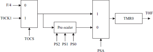
A timer overflow interrupt is generated when the timer register overflows from 255 to 0. This interrupt can be enabled in software by setting bit 5 of the INTCON register. For example, if we wish to generate interrupts at 200μs intervals with a 4 MHz clock, we can select a pre-scaler value of 1 : 4 and enable timer interrupts. The effective timer clock rate will then be 4μs. For a time-out of 200μs, we have to send 200/4= 50 clock pulses to the timer register. Thus, the timer register TMR0 should be loaded with 256− 50 = 206, i.e. a count of 50 before a timer overflow occurs.
The PIC16F84 microcontroller contains a 64-byte nonvolatile EEPROM memory, controlled by registers EEDATA, EEADR, EECON1 and EECON2. There are instructions to read and write the contents of this memory. EEPROM memory is usually used to store configuration data or maximum and minimum data obtained in real-time measurements.
The PIC16F84 microcontroller also contains a configuration register whose bits can be set or cleared during the programming of the device. This register contains bits to select the oscillator mode, to enable or disable code protection, to enable or disable the power-on timer, and to enable or disable the watchdog timer.
3.3.2 PIC16F877 Microcontroller
The PIC16F877 is a 40-pin popular PIC microcontroller. The device offers the following features:
- 8192 × 14 words flash program memory;
- 256 × 8 bytes of EEPROM data memory;
- 368 × 8 RAM data memory;
- eight 10-bit A/D channels;
- 33 bidirectional I/O pins;
- two 8-bit and one 16-bit timers;

Figure 3.18 PIC16F877 pin configuration
- watchdog timer;
- 14 interrupt sources;
- capture, compare and PWM modules;
- on-chip USART;
- 25 mA current source and sink capability.
Figure 3.18 shows the pin configuration of the PIC16F877. I/O ports are accessed as in the PIC16F84 where each port has a direction register (TRIS) which determines the mode of the I/O pins. One of the nice features of the PIC16F877 is that it contains a multiplexed eight-channel A/D converter with 10-bit resolution. A/D conversion is important in microcontroller based control applications, and the operation of this module is described in more detail below.
3.3.2.1 A/D Converter
The eight A/D converter inputs are named AN0–AN7 and are shared with PORTA and PORTE digital inputs as shown in Figure 3.19. There is only one A/D converter and the analog inputs are multiplexed where only one analog input data is converted to digital at any time. Analog inputs can directly be applied to these inputs and the A/D converter generates 10-bit digital signals. The A/D module has four registers:
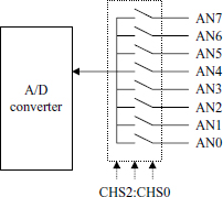
Figure 3.19 A/D converter block diagram
- A/D result high register (ADRESH);
- A/D result low register (ADRESL);
- A/D control register0 (ADCON0);
- A/D control register1 (ADCON1).
The bit definitions of the ADCON0 register are shown in Figure 3.20. This register controls the operation of the A/D converter. The conversion frequency, A/D channels, the A/D status and the conversion command are set by this register.

Figure 3.20 ADCON0 bit definitions
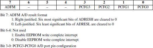
Figure 3.21 ADCON1 bit definitions
The ADCON1 register configures the functions of the A/D input pins and is used to select the A/D converter reference voltage. The bit definitions of ADCON1 are shown in Figure 3.21. Bit 7 of ADCON1 is called the ADFM bit and controls the format of the converted data. When set to 1, the 10-bit result is right-justified and the six most significant bits of ADRESH are read as 0. When ADFM is cleared to 0, the 10-bit result is left-justified with the six least significant bits of ADRESL read as 0. Bits 0–3 of ADCON1 are used to configure the A/D converter input pins as shown in Figure 3.22.
Note that Vref+ and Vref− in Figure 3.22 are the A/D converter positive and negative reference voltages, respectively. The programmer has the choice of using an external reference voltage, but in most applications Vref+ is programmed to be equal to Vdd (the supply voltage) and Vref− is programmed to be equal to Vss (the supply ground).
The A/D conversion operation must be started by setting the GO/DONE bit of register ADCON0. The end of conversion can be detected in one of two ways. The easiest method is to poll the GO/DONE bit continuously until this bit is cleared. The result is then available in register pair ADRESH:ADRESL. The second method is to program the device to generate interrupts when a conversion is complete.
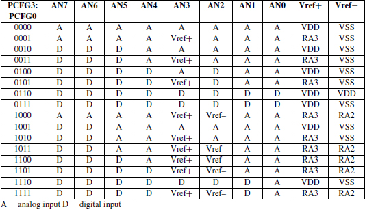
Figure 3.22 A/D converter input pin configuration
The steps required for doing an A/D conversion are listed below:
- Configure the A/D converter module.
- Configure analog pins and reference voltage.
- Select A/D input channel.
- Select A/D conversion clock.
- Turn on A/D module.
- Configure A/D interrupts (if required).
- Start A/D conversion.
- Set GO/DONE bit of ADCON0 to 1.
- Wait for conversion to complete.
- Poll the GO/DONE bit until it is clear or wait for an A/D interrupt.
- Read A/D converter result from ADRESH and ADRESL.
- Repeat the above as required.
3.4 EXERCISES
- Explain the basic features common to all PIC microcontrollers.
- Explain how a PIC microcontroller can be reset using an external push-button switch.
- Draw the circuit diagram of a minimum PIC system using a 4 MHz crystal.
- Draw the circuit diagram of a minimum PIC system using a resistor and a capacitor to generate a clock frequency of about 2 MHz.
- Explain the differences between a crystal and a resonator. Which one would you use if precision timing is required?
- What is a register file map? Where can it be used?
- A PIC16F84 microcontroller is to be used in a system. Port A pins RA0 and RA2 are required to be inputs and all port B pins outputs. Determine the values to be loaded into the port A and port B direction registers.
- Explain the differences between the PIC16F84 and the PIC16F877 microcontrollers.
- How many banks are there in the PIC16F877? Why are there more banks than in the PIC16F84?
- Explain where an A/D converter can be used. How many A/D converter channels are there on the PIC16F877? What are the resolutions of these channels?
- Explain the steps necessary to read data from an A/D channel on the PIC16F877 microcontroller.
- You are required to generate timer interrupts at 120 μs intervals using a 4 MHz crystal as the timing device. Determine the value to be loaded into timer register TMR0. What will be the pre-scaler value?
- Describe the steps necessary to operate the A/D converter to read analog data from channel AN2. What is the format of this data? How can you right-justify the data?
FURTHER READING
[Anon, 2005a] Microchip Data on CDROM. Microchip Technology Inc., www.microchip.com.
[Anon, 2005b] Microchip Databook. Microchip Technology Inc., www.microchip.com.
[Anon, 2005c] PICC Lite User's Guide. Hi-Tech Software, www.htsoft.com.
[Ibrahim, 2002] Ibrahim, D. Microcontroller Based Temperature Monitoring and Control. Newnes, London, 2002.
[Iovine, 2000] Iovine, J. PIC Microcontroller Project Book. McGraw-Hill, New York, 2000.
[James, 1977] James, M.R. Microcontroller Cookbook PIC and 8051. Newnes, London, 1977.
[Kalani, 1989] Kalani, G. Microprocessor Based Distributed Control Systems. Prentice Hall, Englewood Cliffs, NJ, 1989.