
1
The Nanoelectronics Roadmap
James Hutchby
Semiconductor Research Corporation, USA
1.1 Introduction
Over the past 40 years, the global impact of the computer or digital age on most individuals, cultures, and their economies, has been nothing less than breathtaking; it has shifted the communication and human interaction paradigm and has sparked creation of several major new industries. In short, electronics technology based on semiconductor devices and integrated circuits has changed how many of us live our lives and how we do our business.
For example, semiconductor device technology of the 1960s enabled development of large, centralized, power-consuming, main frame computers using discrete transistors to replace vacuum tube binary switches. The 1970s saw the advent of e-mail, desktop and portable calculators, the earliest Internet, digital watches, and the first applications of microprocessors. As complementary metal oxide semiconductor (CMOS) gates became the dominant low-power semiconductor technology in the 1980s, its explosion following Moore's Law1 [1] drove the development and broad application of personal and, later, laptop computers in the 1980s and 1990s. The world's capacity to process bits of information grew from 3.0 × 10⁸ MIPS in 1986, to 4.4 × 10⁹ MIPS in 1993, to 2.9 × 10¹¹ MIPS in 2000, and to 6.4 × 10¹² MIPS in 2007 [2].
Broadened commercial applications in the twenty-first century include Smart Phones, Global Positioning Satellite navigation systems, Digital Cameras, high definition flat panel TVs, tablet PCs, smart dining utensils (for managing food and caloric intake), and a variety of automotive sensor and information-processing electronics.
Much of the commercial success of the semiconductor industry has been driven by its ability to relentlessly follow Moore's Law in doubling the density of transistors every 2–3 years. This phenomenal technology scaling not only enabled new, more complex, applications and lowered the cost per transistor by 25–30%/year [3], it provided faster circuits with lower power dissipation. In this time period, the number of transistors on a chip increased from a few hundred/cm2 to several billion/cm2.
The value of the semiconductor and related electronics systems industries also can be judged by their impact on the United States and global economies. For example, the annual revenues of the semiconductor-based device industry exceeded US$ 300B in 2013, and the related electronics systems industry revenues were projected to exceed US$ 1.55 T in 2010 [4]. Also, from 1960 to 2007, the computer industry added only 0.3% of United States value, but it contributed 2.7% of economic growth and 25% of productivity gains [5].
As these examples illustrate, the rapid and ubiquitous penetration of information-processing technologies into new domains of application and their major economic impact combine to drive aggressive reduction of the size and cost of the basic information-processing element (i.e., the transistor or some new information processing element). However, as the size of the transistor continues to shrink, its structural composition is approaching a few hundred atoms and its operation is becoming prohibitively leaky thus enabling increased power dissipation. Eventually, the semiconductor industry will need a technology to supplement and extend CMOS beyond its fundamental scaling limit.
This raises the following questions: (1) how much further can the present CMOS-based electronics technology be scaled in size and cost; (2) what (if any) new physical mechanism and technology can either supplement, or eventually, replace CMOS as a medium for continued scaling of information-processing technology?
1.2 Technology Scaling: Impact and Issues
Scaling CMOS raises some additional important issues regarding increased power dissipation of aggressively scaled metal oxide semiconductor field effect transistors (MOSFETs) leading to unwieldy power density dissipated on a silicon CMOS chip. Historically, one could reduce the threshold voltage and, thereby, the source–drain voltage and power dissipation of a scaled MOSFET transistor in a CMOS gate. However, in recent years the allowable threshold voltage of a MOSFET has reached a minimum of 0.9–1.0 V. Consequently, as the transistor is further scaled its power dissipation increases. The power dissipation on a scaled chip has two sources. One source is the scaled transistors. The other source is the system of metal interconnects.
The physical operation of electronic devices ranging from the vacuum tube, to a variety of transistors and integrated circuits, has centered on the manipulation and storage of electronic charge. The next section discusses the limits of charge confinement and relates them to a fundamental scaling limit of CMOS.
1.3 Technology Scaling: Scaling Limits of Charge-based Devices
Operation of MOSFETs is based on manipulation of electronic charge transport from source to drain controlled by another charge placed on a gate [6]. Electrons placed on the source are prohibited (for the most part) from flowing spontaneously to the drain by an energy barrier formed by the gate/source and the source/drain potentials. Lowering this energy barrier by placing a positive charge on the gate allows electrons on the source to flow to the drain when assisted by a forward bias voltage. Conversely, these electrons on the drain are blocked from returning to the source by the drain/source energy barrier. The question then is: What is the minimum height (Eb) and width (a) of the gate/source potential energy barrier necessary to allow an electron to have equal probability of being either in the source or the drain?
Figure 1.1a illustrates manipulation of the energy barrier between the source and drain of a MOSFET by application of a voltage, Vgs, from the gate to the source, and another voltage, Vds, from the drain to the source. Altering these voltages changes the height and, to a lesser extent, the width of this energy barrier and, thereby, changes the confinement of electronic charge in either of two potential wells. One is defined by the source and the other by the drain. An idealized model of this source–gate–drain potential well structure is illustrated in Figure 1.1b.

Figure 1.1 Energy model for limiting device. (a) Cross-section of a MOSFET illustrating potential distributions and their effect on the potential barrier separating the source drain potential wells. (b) Idealized model of the potential barrier separating the source drain potential wells where: w = width of left-hand well (LHW) and right-hand well (RHW); a = barrier width; Eb = barrier energy
The model illustrated in Figure 1.2 is used to estimate the minimum width, amin, and height, Ebmin, needed to provide a 50% probability that a single electron is either in the source or drain potential well. Figure 1.2 also illustrates two processes for transmitting electrons either over the barrier by thermionic emission or through the barrier by quantum mechanical tunneling. Using these criteria, a limit value of a, amin = 1.5 nm and Ebmin = kTln2, where k is the Boltzmann constant, and T is absolute temperature in degrees Kelvin. An additional constraint requiring minimization of energy dissipated in changing potential wells sets amin = 5 nm.
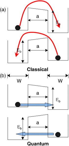
Figure 1.2 Illustration of two processes for transmitting electrons either (a) over an energy barrier by thermionic emission, or (b) through the barrier by quantum mechanical tunneling
Since high-volume manufacturing technology for the 16 nm node is currently being ramped to full production, the 5 nm generation may go into manufacturing in 7 years or in 2020. The 8 nm generation may be in manufacturing as early as 2018. Consequently, scaling of CMOS-based information-processing technology will face fundamental limits within the next 5–7 years or by 2020. This determines a need to have any new technology for extending CMOS in place by that time. Furthermore, this analysis suggests that the search for a new information-processing technology and paradigm should consider a new “token” to replace the electronic charge or a new information-processing paradigm that does not depend on confinement of the electronic charge.
1.4 The International Technology Roadmap for Semiconductors
Formed in 1991 by the United States Semiconductor Industry Association (SIA) assisted by Semiconductor Research Corp. (SRC) and SEMATECH, the United States National Technology Roadmap for Semiconductors (NTRS) brought together scientists and technologists from the United States microelectronics manufacturing, supplier, and academic communities and tasked them to forecast technological scaling of MOSFET integrated circuits and all related technologies 15 years into the future. The first NTRS was published in 1992.
Recognizing the value of including international microelectronics communities, the International Roadmap Committee (IRC) established the International Technology Roadmap for Semiconductors (ITRS) in 19982. The ITRS was tasked to develop and maintain a 15 year assessment of the semiconductor industry's future technology requirements. These future needs drive present-day strategies for world-wide research and development among manufacturers' research facilities, universities, national laboratories, and tool manufacturers in 17 topical areas ranging from basic or emerging research materials and emerging research devices to design and systems drivers. This book is focused on Emerging Research Devices.
1.5 ITRS Emerging Research Devices International Technology Working Group
As the size of the transistor continues to shrink, its structural composition is approaching a few hundred atoms and its operation is becoming prohibitively leaky, thereby leading to increased power dissipation. Briefly mentioned above, the semiconductor industry eventually will need a technology to supplement and extend CMOS beyond its fundamental scaling limit and one day even to replace CMOS.
As this need took on some urgency, the ITRS International Roadmap Committee (the ITRS governance committee) formed a new technical work group; this group became the Emerging Research Devices (ERD) International Technology Working Group (ITWG).
1.5.1 ERD Editorial Team
The ERD International Technology Working Group (ERD ITWG) is a large international group of approximately 80 individuals who contribute in some way to the work of the ERD Team over a 2 year cycle to produce a new ERD chapter for each updated ITRS. The ERD Editorial Team consists of approximately 12 actively engaged individuals, 8 of whom represent eight companies, 2 represent two universities, and 2 represent one consortium. This Editorial Team provides leadership for the ERD ITWG. Many ERD active contributors manage research groups that address nanoelectronics topics within their organizations and a few members of ERD are actively engaged practicing researchers contributing to this field. Much of the text in the ERD chapter is written by practicing researchers well-recognized for their leadership in the field in which they make their contributions. Their contributions are then vetted by the ERD Editorial Team and the IRC to ensure balance and accuracy of any claims or projections made for a Technology Entry.
1.5.2 Vision and Mission
The vision of the ERD is to assist the nanoelectronics research community to invent and demonstrate feasibility of new technologies to extend information processing beyond the reach of Si technology and to be a resource to the Semiconductor Industry in their evaluation of these nanodevices.
The mission of the ERD ITWG is to offer substantive input to our reader communities related to the viability of proposed nanoelectronic devices to live up to their claimed potential in heir maturity. The targeted reader communities include the global research community (including industrial, university, and government laboratories), relevant government agencies, industry technology directors and managers, and the supplier communities. ERD evaluates significant new concepts for nanodevices proposed to supplement and/or replace the silicon MOSFET for information processing. This is accomplished by critically assessing the suitability and maturity of a nanodevice concept for sustaining information processing beyond that attainable with ultimately scaled CMOS thereby leading to promising new approach(es) to memory and logic technologies to be implemented by 2020–2026.
1.5.3 Scope
The scope of ERDs activities embraces evaluating emerging research memory (including solid state storage), logic, information processing, More-than-Moore, and new nanoarchitecture technologies enabled by promising new nanodevices together with the requisite materials and process technologies chosen to fabricate the device and test structures [in collaboration with the Emerging Research Materials (ERM) work group].
Evaluation of a candidate nanodevice includes assessing its scaling potential, power dissipation, speed, operation temperature, internal gain, technological, and/or architectural compatibility with CMOS. The primary question addressed by this evaluation process is: “Assuming a device reaches its full maturity in fabrication and operation, how would it compare with ultimately scaled CMOS and to what extent can it be scaled further?” Evaluation also includes identifying the most important scientific and technological questions and issues that must be resolved to advance acceptance of the device for further attention and accelerated development. The scope includes modeling and simulation and those metrologies required by the research community to establish and demonstrate the operation and feasibility of a new device.
Evaluation is further discussed in Section 1.6.1.
1.6 Guiding Performance Criteria
1.6.1 Nanoinformation Processing
First, we need a clear understanding of just what is meant by “information.” Webster's New International Dictionary defines information for broad popular use as “the communication or reception of knowledge or intelligence.” For focused digital computing and digital signal-processing applications, information is defined in its most restricted technical sense “as a sequence of symbols that can be interpreted as a message.” These symbols take on a specific meaning when they are encoded according to a particular algorithm. The questions addressed by the ERD work group in considering a proposed new technology include:
- In a new technology, how can a single bit of information be physically represented – what is the operative information-bearing token?” (e.g., the electron in electronic circuits or the bead in an abacus.)
- What property of the information “token” is used as the “state variable” to define and sense the state? (e.g., for an electron the commonly used state variable is charge and its presence/absence is sensed by a voltage across the drain load capacitance.3 For the abacus the state variable is the mass and physical position of a bead.)
- How can the state variable be manipulated to reliably change the logic state? (e.g., in a CMOS gate the voltage of the load capacitor can be increased and decreased by placement and removal of electrons on to and off of the load capacitor. For the abacus it is the movement of a bead to and from a defined position.)
- How can the state variable in one position communicate with a state variable in another position to perform a function? (e.g., in CMOS, copper metal interconnect wires conduct charge/voltage from one site another, and in an abacus, nimble fingers perform the task of moving a bead from one position to another.)
- What is the performance claimed for the new technology in terms of its power dissipation, switching speed, and so on? How does this compare with the performance of ultimately scaled silicon?
- What fabrication and manufacturing issues need to be addressed and resolved?
- What fundamental and technology issues need to be addressed and resolved to demonstrate the promise and feasibility of the proposed technology?
1.6.2 Nanoelectronic Device Taxonomy
Information processing to accomplish a specific system function, in general, requires several different interactive layers of technology. The objective of this section is to carefully delineate a taxonomy of these layers to further distinguish the scope of this book from that of the Emerging Research Materials chapter and the Systems Design chapter in the ITRS. The scope of this book addresses the Device and the Data Representation layers shown in Figure 1.3.
One comprehensive top-down list of these layers begins with the required application or system function, leading to system architecture, micro- or nanoarchitecture, circuits, devices, and materials. As shown in Figure 1.3 a different bottom-up representation of this hierarchy begins with the lowest physical layer represented by a computational or information token (e.g., the electron) and ends with the highest layer represented by the architecture. In this more schematic representation, focused on generic information processing at the device/circuit level, a fundamental unit of information (e.g., a bit) is represented by the value of a property (e.g., presence or absence of electronic charge or the polarity of spin) of a computational information token, for example, the position of a bead in the ancient abacus calculator or the electronic charge or voltage state of a nodal capacitance in CMOS logic. A device provides the physical means of representing and manipulating a property (e.g., position of an electronic charge) of a computational information token among its two or more allowed discrete states. Eventually, device concepts may transition from simple binary switches to devices with more complex information processing functionality.
The device is a physical structure resulting from the assemblage of a variety of materials possessing certain desired properties obtained through exercising a set of fabrication processes. An important layer, therefore, encompasses the various materials and processes necessary to fabricate the required device structure, which is the domain of the ERM International Technical Work Group. The data representation layer is how the state variable property of the information token is encoded by the assemblage of devices to process the bits or data. Two of the most common examples of data representation are binary digital and continuous or analog signaling. In some cases, the data are represented as arrays or images which then become the fundamental datum of computation in either primitive or compressed form. This layer is within the scope of the ERD ITWG. The architecture plane encompasses three subclasses of this taxonomy: (1) the nanoarchitecture or physical arrangement or assemblage of devices to form higher level functional primitives to represent and enable execution of a computational model, (2) the computational model that describes the algorithm by which information is processed using the primitives, for example, logic, arithmetic, memory, cellular nonlinear network (CNN), and (3) the system-level architecture that describes the conceptual structure and functional behavior of the system exercising the computational model. Subclass (1) is within the scope of the ERD Technical Work Group, and subclasses (2) and (3) are within the scope of the Design Technical Work group. The elements shown in the red-lined yellow boxes (left side of Fig. 1.3) represent the current CMOS platform technology that is based on electronic charge as a binary information token. This state token serves as the foundation for the von Neumann computational system architecture. Analog data representation also is included in the current CMOS platform technology. The other entries grouped in these five categories summarize individual approaches that, combined in some yet to be determined highly innovative fashion, may provide a new highly scalable information-processing paradigm.

Figure 1.3 Taxonomy for nanoinformation processing devices
1.6.3 Fundamental Guiding Principles – “Beyond CMOS” Information Processing
In considering the many disparate new approaches proposed to provide order of magnitude scaling of information processing beyond that attainable with ultimately scaled CMOS, the ERD Editorial Team proposed the following comprehensive set of guiding principles. We believe these “Guiding Principles” provide a useful structure for directing research on any information-processing technology to dramatically enhance scaling of functional density and performance while simultaneously reducing the energy dissipated per functional operation. Further this new technology would need to be realizable using a highly manufacturable fabrication process.
1.6.3.1 Computational Information Variable(s) other than Solely Electron Charge
In seeking new device opportunities, it is important to understand not only the device characteristics, but also how connected systems of these devices might be used to perform complex logic functions [7]. The basic computational element in current digital information processing systems is the binary switch. In its most fundamental form, it consists of:
- Two states 0 and 1 (state variables), which are equally attainable and distinguishable;
- A means to control the change of the state (WRITE);
- A means to read the state;
- A means to communicate with other binary switches (TALK).
The system state representation controls (WRITE), and the READ and TALK operations are all represented by a physical property of entities such as particles, quasi-particles, collections of particles, and so on. These physical entities are called tokens. Each token has a set of physical attributes associated with it (e.g., charge, mass, spin) and it is the physical interaction between the token attributes within the device structure that determines the operation and the resulting state of the device. In most cases, an attribute can assume several values and for this reason, we also call them state variables.
The estimated performance comparison of devices utilizing an alternative token (e.g., an electron, position of an atom) with an alternative “state variable” (e.g., charge and voltage, spin, current) to ultimately scaled CMOS should be made as early in a program as possible to down-select and identify key trade-offs.
1.6.3.2 Nonthermal Equilibrium Systems
These are systems that are out of equilibrium with the ambient thermal environment for some period of their operation, thereby reducing the perturbations of stored information energy in the system caused by thermal interactions with the environment. The purpose is to allow lower energy computational processing while maintaining information integrity.
1.6.3.3 Novel Energy Transfer Interactions
These interactions could provide the interconnect function between communicating information processing elements. Energy transfer mechanisms for device interconnection could be based on short-range interactions including, for example, quantum exchange and double exchange interactions, electron hopping, Förster coupling (dipole–dipole coupling), tunneling and coherent phonons.
1.6.3.4 Nanoscale Thermal Management
This could be accomplished by manipulating lattice phonons for constructive energy transport and heat removal.
1.6.3.5 Sublithographic Manufacturing Process
One example of this principle is directed self-assembly of complex structures composed of nanoscale building blocks. These self-assembly approaches should address nonregular, hierarchically organized structures, be tied to specific device ideas, and be consistent with high-volume manufacturing processes.
1.6.3.6 Alternative Architectures
In this case, architecture is the functional arrangement on a single chip of interconnected devices that includes embedded computational components. These architectures could utilize, for special purposes, novel devices other than CMOS to perform unique functions.
1.6.4 Current Technology Requirements for CMOS Extension and Beyond CMOS Memory and Logic Technologies
Some emerging nanoscale devices discussed in this book are charge-based structures proposed to extend CMOS to the end of the current roadmap. Other emerging devices offer new computational information “tokens” and will likely require new fabrication technologies.
A set of relevance or evaluation criteria, defined below, are used to parameterize the extent to which proposed “CMOS Extension” and “Beyond CMOS” technologies are applicable to memory or information-processing applications. The relevance criteria are: (1) scalability, (2) speed, (3) energy efficiency, (4) gain (logic) or ON/OFF ratio (memory), (5) operational reliability, (6) operational temperature, (7) CMOS technological compatibility, and (8) CMOS architectural compatibility. Definitions of these evaluation criteria follow:
- 1. Scalability: First and foremost the major incentive for developing and investing in a new information-processing technology is to discover and exploit a new domain for scaling information-processing functional density and throughput per Joule substantially beyond that attainable by ultimately-scaled CMOS. Silicon-based CMOS has provided several decades of scaling of MOSFET densities. The goal of a new information-processing technology is to replicate this success by providing additional decades of functional and information throughput rate scaling using a new technology. In other words, it should be possible to articulate a Moore's Law for the proposed technology over additional decades.
- 2. Speed: A future information-processing technology must continue to provide (at least) incremental improvements in speed beyond that attainable by ultimately scaled CMOS technology. In addition, nanodevices that implement both logic and memory functions in the same device would revolutionize circuit and nanoarchitecture implementations.
- 3. Energy Efficiency: Energy efficiency has become the limiting factor of any beyond CMOS device using electronic charge or electric current as a computational information token used to represent a state variable. It also appears that it will be a dominant criterion in determining the ultimate applicability of alternate state variable devices. Clock speed versus density trade-offs for electron transport devices will dictate that for future technology generations; clock speed will need to be decreased for very high densities or conversely, density will need to be decreased for very high clock speeds. Nanoscale electron transport devices will best suit implementations that rely on the efficient use of multi-core processing to minimize energy dissipation.
- 4a. Ion/Ioff Ratio (Memory Devices): The Ion/Ioff ratio of a memory device is the ratio of the resistance of a memory storage element in the Ion state to its resistance in the Ioff state. For nonvolatile memories, the Ion/Ioff ratio represents the ratio between the read current of a selected memory cell to the leakage current of an unselected cell. In cross-point memories, a very large Ion/Ioff ratio is required to minimize power dissipation and maintain adequate read signal margin.
- 4b. Gain (Logic Devices): The internal gain of nanodevices is an important limitation for presently used combinatorial logic where gate fan-outs require significant drive current and low voltages make gates more noise sensitive. New logic and low fan-out circuit approaches will be needed to use most of these nanodevices for computing applications. Signal regeneration for large circuits of nanodevices may need to be accomplished by integration with CMOS.
- 5. Operational Reliability: Operational reliability is the ability of the memory and logic devices to operate reliably within their operational error tolerance given in their performance specifications. The error rate of all nanoscale devices and circuits is a major concern. These errors arise from the difficulty of providing highly precise dimensional control needed to fabricate the devices and also from interference from the local environment. Large-scale and powerful error detection and correction schemes will need to be a central theme of any architecture and implementations that use nanoscale devices.
- 6. Operational Temperature: Nanodevices must be able to operate close to a room temperature environment for most practical applications with sufficient tolerance for higher temperature (e.g., 100 °C) operation internal to the device structure.
- 7. CMOS Technological Compatibility: The semiconductor industry has been based for the last 40 years on incremental scaling of device dimensions to achieve performance gains. The principal economic benefit of such an approach is it allows the industry to fully apply previous technology investments to future products. Any alternative technology as a goal should utilize the tremendous investment in infrastructure to the highest degree possible. Furthermore, in the near term, integratability of nanodevices with silicon CMOS is a requirement due to the need for signal restoration for many logic implementations and to be compatible with the established technology and market base. This integration will be necessary at all levels from design tools and circuits to process technology.
- 8. CMOS Architectural Compatibility: This criterion is motivated by the same set of concerns that motivate the CMOS technological compatibility, namely the ability to utilize the existing CMOS infrastructure. Architectural compatibly is defined in terms of the logic system and the data representation used by the alternative technology. CMOS utilizes Boolean logic and a binary data representation and, ideally, an alternative technology would need to do so as well.
1.7 Selection of Nanodevices as Technology Entries
Candidate Technology Entries are identified through a variety of means including a minimum of four workshops held in each 2 year cycle, extensive literature searches, personal knowledge of ERD ITWG members, ERD critiques, and so on.
These candidate Technology Entries are considered for inclusion in the ITRS ERD chapter based on their potential for accomplishing the objectives for a new technology, level of published research activity, credibility, and progress. In addition a candidate Technology Entry should have attained significant maturity in its research domain. Its continued inclusion is governed by progress in resolving those research issues gating demonstration of feasibility.
In addition to the requirements discussed above, specific criteria for including a Technology Entry in any one of the Research Devices and Architectures sections are: (1) research on the proposed Technology Entry is published by two or more groups in archival literature and peer reviewed conferences, or (2) research on the proposed Technology Entry is published extensively by one group in archival literature and in peer reviewed conferences.
1.8 Perspectives
Development and scaling of CMOS over the past 40+ years has revolutionized many aspects of our lives and has been a driver of the world-wide economy. We communicate globally at any time using a paper-thin computer–telephone, no larger than a wallet, with the computational power far exceeding that of a dated mainframe computer. Similar hand-held devices coupled to a complex satellite network system (Global Positioning System or GPS) can locate our position with an accuracy of a few feet and can navigate us through completely unknown terrain (e.g., a large metropolitan area or an arid desert). Soon automobiles will be able to talk to each other to operate an automobile safely making the human driver obsolete. These technologies have been enabled by ever-shrinking MOSFETs providing lower cost, higher speed, and lower power dissipation per transistor in silicon-based integrated circuits. Scaling of silicon MOSFETs will likely continue to the 8 nm, and possibly even to the 5 nm technology generation, at which point individual MOSFETs will have reached their fundamental scaling limit defined by the relatively small number of atoms making up a transistor.
Given this approaching limit on physical scaling of the MOSFET structure and its properties, how can the semiconductor industry continue to provide lower cost, higher density, and higher performance ICs? In the relative short-term, the design community will continue its efforts and successes to obtain performance gains and cost savings by deriving more value from current technology. Also, some important applications can be addressed by current technology for speed, but need lower power dissipation, at a lower cost per chip (e.g., a smart cell phone). Also, More-than-Moore technology, in which current IC technology is integrated with other current technologies (e.g., sensors, RF components) on a circuit board or in a package, is being used to provide many functions for new applications.
In the longer term, a new information-processing technology, capable of providing additional scaling of the primitive element's size, cost, and power dissipation together with increased data throughput, would have invaluable impact. Undoubtedly, it would set off the discovery of another round of new applications, some opening completely new possibilities such as nanomorphic microsystems used in vivo to diagnose and attack disease cells [8].
Perhaps Kroemer had the best perspective on application of a new technology when in his Nobel Lecture he stated [9]: “The principal applications of any sufficiently new and innovative technology always have been – and will continue to be – applications created by that technology.”
So, as a community of pioneers seeking to discover a new information-processing technology, let us remain alert to new applications for our current findings.
Notes
References
- 1. Moore, G.E. (1965) Cramming more components onto integrated circuits. Electronics Magazine, 38, 3–6.
- 2. Wikipedia (2014) http://en.wikipedia.org/wiki/Information_Age (accessed 16 January 2014).
- 3. Jefferies (2014) http://jefferies.com/CMSFiles/Jefferies.com/files/Insights/Moore%20Stress_Structural%20Industry%20Shift_09272012.pdf (accessed 16 January 2014).
- 4. Cellular News (2014) http://www.cellular-news.com/story/43209.php (accessed 16 January 2014).
- 5. Jorgenson, D.W., Ho, M., and Samuels, J. (2014) http://scholar.harvard.edu/files/jorgenson/files/02_jorgenson_ho_samuels19nov20101_2.pdf (accessed 16 January 2014).
- 6. Zhirnov, V.V., Cavin, R.K. III, Hutchby, J.A., and Bourianoff, G.I. (2003) Limits to binary logic switch scaling – A gedanken model. Proceedings of the IEEE, 91 (11), 33–36.
- 7. Zhirnov, V.V., Cavin, R.K. III, and Bourianoff, G.I. (2010) New State variable opportunities beyond CMOS: A system perspective, in Emerging Technologies and Circuits (eds A. Amara, T. Ea, and M. Belleville), Springer.
- 8. Zhirnov, V.V. and Cavin, R.K. III (2010) Microsystems for Bioelectronics: the Nanomorphic Cell, Elsevier Press.
- 9. Kroemer, H. in his Nobel Lecture (8 December 2000) Quasi-Electric Fields and Band Offsets: Teaching Electrons New Tricks, Aula Magna, Stockholm University.