
17
Spintronics
Alexander Khitun
Material Science and Engineering, University of California, USA
17.1 Introduction
Spintronics, also known as magnetoelectronics, is an emerging technology exploiting both the intrinsic spin of the electron and its associated magnetic moment, in addition to its fundamental electronic charge, in solid-state devices [1]. Either adding the spin degree of freedom to conventional charge-based electronic devices or using the spin alone has the potential advantages of nonvolatility, increased data processing speed, decreased electric power consumption, and increased integration densities compared with conventional semiconductor devices [2]. Spintronics originates from research on the influence of spin on electrical conduction in ferromagnetic metals by Mott in 1936, Fert and Campbell in 1968, and gained further momentum with the discovery of spin-dependent electron transport phenomena in the 1980s. The notable milestones of Spintronics development include the observation of spin-polarized electron injection from a ferromagnetic metal to a normal metal by Johnson and Silsbee [3], and the discovery of giant magnetoresistance (GMR) independently by Albert Fert et al. [4] and Peter Grünberg et al. [5]. Pioneered by IBM in 1997, the GMR head enabled hard-disk drives to read smaller data bits, which led to a more than 40-fold increase in data storage density over the past seven years [6]. Today, the area of Spintronics is expanding considerably by considering spin-based phenomena, that is, spin transfer torque [7], and by introducing novel materials, that is, graphene spintronics [8] and molecular spintronics [9].
Spintronics has been recognized as one of the emerging technologies able to provide the continuation of the functional throughput enhancement [10]. On the one hand, the potential advantages of using the additional degree of freedom provided by spin are indisputable. On the other hand, the utilization of spin-based devices has to follow the mainstream of conventional electron-based devices and provide a substantial performance improvement in order to justify the technological difficulties associated with combining the two technologies. How do we utilize spin in the most efficient way? And how should we integrate novel spin-based devices with the traditional transistor-based logic circuitry? These are the main questions to be answered.
Current efforts in developing spintronic logic devices involve two major approaches. The first approach is to build a spin transistor enabling lower power consumption and higher functional throughput than the scaled CMOS. This approach originates from the first proposal on the electro-optical modulator proposed by Datta and Das in 1990 [11] and has resulted in a great deal of research during the past two decades. This direction is pretty straightforward as it would continue the mainstream of conventional logic circuitry development as it worked for the past seven decades. There is a variety of spin transistors proposed so far, which can be classified into two types: the spin-FET proposed by Datta and Das (and its modified versions [12,13]) and the spin-MOSFET with several variations [14,15]. The spin-FET type transistors are aimed to take advantage of spin-polarized current modulation via spin–orbit coupling and build a transistor with unique output characteristics (i.e., output current oscillates as a function of the gate voltage). Another type of spin transistor called the spin-MOSFET resembles the conventional MOSFET with magnetic elements included. The incorporation of magnetic elements in the conventional field effect transistor structure offers advantages in both energy saving and logic functionality [15]. Besides these two major groups, there are multiple proposals to use organic materials, graphene (as the channel), and hybrid schemes combining conventional MOSFET with magnetic tunneling junction (MTJ) [16].
The second approach, which is more radical, focuses on the utilization of spin as a logic state variable. In theory, logic 0 and 1 can be assigned to the polarization of a single spin placed it in a magnetic field (so-called Single Spin Logic [17,18]). Such a logic representation promises additional functionalities beyond the capabilities of the conventional FET. A spin system can be maintained in a nonequilibrium state longer than a charge system due to the weaker spin-phonon coupling, which translates in low power consumption for low-duty cycle applications [19]. Single spin logic possesses similar problems as for single electron logic, namely high sensitivity to the structure imperfections and thermal fluctuations. More practical proposals are aimed at utilizing the collective states of a large number of spins coupled via the exchange interaction (i.e., nanomagnetic logic [20]). Theoretically, switching between the collective spin states would require the same amount of energy as for a single spin state, though the collective state would be more immune to noise. Nonvolatility (ability to preserve the result of computation without an external power source) is the key advantage offered by the nanomagnetic logic thus reducing static power consumption, which is the critical problem of the charge-based approach.
While there are promising potential advantages to using spin-based logic devices, a number of questions remain open. In this section, we describe the principle of operation, the current status of development of the spin-based logic devices and we discuss the potential advantages and key technological issues limiting the performance of these devices and Spintronics in general.
17.2 Spin Transistors
Spin transistors constitute a special type of semiconductor transistor combining conventional transistor behavior with the functionalities of a magnetoresistive device. The important features of spin transistors are: (i) variable drive current controlled by the magnetization configuration of the ferromagnetic electrodes, and (ii) nonvolatile information storage using the magnetization configuration. These features are very useful functionalities for the goal of achieving highly energy efficient, low-power circuit architectures that are inaccessible to ordinary CMOS circuits [10].
17.2.1 Spin-FETs
It would be fair to say that the development of spin transistors has started from the proposal of the semiconductor electron wave analog of the electro-optic modulator proposed by Datta and Das [11], as shown in Figure 17.1. This is a three-terminal electronic device with source, drain, and gate contacts, where the source to drain current is controlled by applying a gate voltage. At first look, this device is very similar to the ordinary semiconductor transistor. However, the principle of operation of the spin-FET is completely different from the conventional transistors. The source and the drain are made of a ferromagnetic (or half-metallic) material working as polarizer and analyzer for the spin polarized current. The electrons are injected into a quasi one-dimensional semiconductor channel from the magnetic source. The initial spin polarization of the injected spins is supposed to be parallel to the polarization of the source. Then, the precession of the injected spins in the channel is controlled with a gate potential via the Rashba spin–orbit coupling effect. The precession angle θ is defined by the following [11]:
where m* is the effective electron mass, parameter α is the spin orbit coupling coefficient, L is the channel length, ![]() is Planck's constant. The probability that the electrons will be transmitted through the channel/drain interface depends on the relative orientation of the electron's spin with the drain magnetization and the rate of precession controlled by the gate voltage. This probability is maximized when the polarization of the incoming electrons is parallel to the magnetization of the drain (θ = 0), and the probability is at a minimum where the polarization of the incoming electrons and the drain are antiparallel (θ = π). Thus, the source–drain current oscillates as a function of the gate voltage similar to the intensity modulation in the electro-optic modulators.
is Planck's constant. The probability that the electrons will be transmitted through the channel/drain interface depends on the relative orientation of the electron's spin with the drain magnetization and the rate of precession controlled by the gate voltage. This probability is maximized when the polarization of the incoming electrons is parallel to the magnetization of the drain (θ = 0), and the probability is at a minimum where the polarization of the incoming electrons and the drain are antiparallel (θ = π). Thus, the source–drain current oscillates as a function of the gate voltage similar to the intensity modulation in the electro-optic modulators.

Figure 17.1 Schematics of the semiconductor electron wave analog of the electro-optic modulator – the first proposed Spin FET. Reprinted with permission from [11]. Copyright 1990, American Institute of Physics
Efficient spin injection into the semiconductor channel, long spin coherence length in the channel, strong Rashba coupling for spin polarization control and low scattering are the key requirements for spin-FET operation. The efficiency of the spin injection is defined by the spin polarization η: η = (N↑ − N↓)/(N↑ + N↓), where N↑ and N↓ is the number of the injected spin up and spin down electrons. In the ideal scenario, all of the injected electrons are of the same spin polarization η = 1. However, it is difficult to achieve high efficiency of spin injection from an ordinary ferromagnet (i.e., a ferromagnetic metal) to a semiconductor due to the conductivity (or impedance) mismatch problem [21]. This problem originates from the large difference in electrical conductivity between a ferromagnetic metal and a semiconductor. A possible solution to this problem is via the introduction of insulating tunnel barriers between the ferromagnetic and semiconductor, or making Schottky contacts with highly doped semiconductor thin layers [22]. Spin injection in the material systems with InxGa1−x, as have been studied widely and extensively during the past decade. Typically, experimentally detected spin polarization does not exceed a few percentage points with spin diffusion length Ls of several microns (i.e., η ∼ 5.7%, Ls ∼ 5.1 μm at 1.5 K [23]).
Being injected into a semiconductor channel, the spins of conduction electrons are subject to different relaxation mechanisms (i.e., Elliott–Yafet [24], D'yakonov–Perel' [25], Bir–Aronov–Pikus [26]) which reduce spin polarization. The most critical are the Elliott–Yafet relaxation processes due to scattering via phonons, impurities, boundaries, which are inherent in all semiconductors, and the D'yakonov–Perel' mechanism in compound semiconductors without a center of inversion symmetry, which is most prominent in III-V compound semiconductors. All the scattering mechanisms tend to equalize the number of spin up and spin down electrons in a nonmagnetic semiconductor channel. In turn, the decrease of spin polarization within the ensemble of conducting electrons reduces the On/Off ratio. For spin-FETs, it is critical to suppress the spin relaxation in the channel while keeping the maximum strength of the spin–orbit interaction. The suppression of spin relaxation can be achieved via electron confinement (i.e., making one-dimensional channel structures whose characteristic size is less than the bulk spin diffusion length) [27], or by utilizing the so-called persistent spin helix (PSH) condition [28]. In the PSH condition, spin polarization is conserved even after scattering events. This conservation is predicted to be robust against all forms of spin independent scattering, including electron–electron interaction. Recently, the PSH condition has been experimentally realized and spin life time enhancement by two orders of magnitude was observed near the exact PSH point (as shown in Figure 17.2) [29]. Though these experimental data demonstrate a significant progress towards the spin control in semiconductors, the achieved spin lifetime (10–100 ps) is still not long enough for any practical application.

Figure 17.2 (a) Temperature dependence of the spin–orbit enhanced (τE) and spin–orbit reduced (τR) lifetimes of helix modes for the 11-nm GaAs quantum wells closest to the PSH regime. (b) Temperature dependence of the dimensionless lifetime enhancement factor η for each helix mode. (c) Temperature dependence of the PSH dispersion curves for a similar sample with a slightly reduced mobility. Reprinted by permission from [29]. Macmillan Publishers Ltd, Copyright 2009
Besides efficient spin injection and long spin coherence length, spin-FETs require certain channel materials with a strong spin–orbit interaction such as InGaAs, InAs, and InSb. The stronger the spin–orbit coupling α, the shorter is the channel length L at which spin polarization can be π-rotated at a given gate voltage (Eq. Eq. (17.1)). There are two kinds of spin–orbit interactions known as: (i) the Dresselhaus spin–orbit interaction [30], which originates from the lack of an inversion asymmetrical lattice structure, and (ii) the Rashba spin–orbit interaction [31], which originates from the sum of the effective electric fields at the interfaces and inside the confined structure. During the past two decades, Rashba spin–orbit interaction has been widely discussed and investigated [32]. The strength of the spin–orbit coupling is usually determined from observation of beatings in the Shubnikov–de Haas (ShdH) oscillations [33–35], the measurement of magnetoresistance in the regime of weak anti-localization in low magnetic fields [36], by the observation of Zeeman splitting energies in confined structures [37], as well as by analyzing the Raman spectrum [38], spin resonance [39] and cyclotron resonance [40]. It should be noted that the voltage-controlled spin–orbit interaction may come from the competition of two or more mechanisms (e.g., the change of the carrier concentration, or the modification of the confined electron's wave function). For example, the experimental data for In0.75Ga0.25As/In0.75Al0.25As hetero-structure show α to be almost constant near zero gate voltage and its decrease with negative Vg due to the change of the carrier concentration [33]. In contrast, the coupling constant α increases with the increase of negative gate voltage due to the modification of quantum well potential in a strained InGaAs/InP quantum wire [34]. In all cases, the maximum observed value of spin–orbit coupling strength does not exceed the tens of 10−12 eVm, which implies certain limits on the gate length required for a π-phase modulation according to Equation 17.1. For example, taking α = 10 × 10−12 eVm and the effective mass m* = 0.05, the minimum gate length of spin-FETs is 260 nm [41]. Theoretically, the strength of spin–orbit coupling can be enhanced by using the PSH condition where the total effective magnetic field induced both by the Rashba spin–orbit interaction and the Dresselhaus spin–orbit interaction is doubled, reducing the length by half. It is also expected that gate length can be reduced for p-type spin FETs due to the larger spin–orbit interaction value and gate controllability [42]. It is important to note, that the channel length of spin-FETs (the length required for π-phase modulation) must be shorter than the spin scattering length, which is a grand challenge for building room temperature operating prototypes.
The first working spin-FET prototype based on an InAs heterostructure was demonstrated in 2009 [43]. The prototype resembles a conventional lateral spin valve device for nonlocal measurements with two Ni81Fe19 electrodes on top of an InAs high-mobility channel (μ > 50 000 cm2 V−1 s−1) of length 1.65 μm. This device shows an oscillatory conductance as a function of the applied voltage as was originally predicted by Datta and Das [11]. However, the origin of the observed spin signals is not yet clear [44–46]. Overall, efforts to implement a Datta–Das spin transistor operating at room temperature have not yet been successful. In spite of great efforts by multiple research groups, spin-FETs are far from practical realization due to the problems associated with efficient spin injection and control, and the lack of the efficient control of the spin precession by a gate voltage. It is expected that there will be further progress in improving spin injection efficiency and spin relaxation suppression. However, the low strength of the spin–orbit coupling will remain the main fundamental problem making spin-FETs inferior to conventional CMOS.
17.2.2 Spin-MOSFETs
The problems with spin precession control by applying an electric field have stimulated further search for spin transistors the operation of which does not rely on weak spin–orbit coupling. This class of spin transistors is known as spin-MOSFETs [14]. In contrast to spin-FETs, the channel of spin-MOSFET is composed of silicon with a very weak spin–orbit interaction. There is no voltage-controlled spin polarization rotation required for spin-MOSFET operation. Current modulation through the channel is achieved in a way similar to the ordinary MOSFET by changing the carrier concentration in the channel, though the concentration of spin up and spin down electrons may differ significantly due to the spin-dependent band structure. In contrast to spin-FETs with a fixed source/drain magnetic configuration, it is assumed that the magnetization of the source and drain in spin-MOSFETs can be changed during operation and provide additional control of the output current. The latter opens a variety of ways for spin-MOSFET construction by implementing different materials for the source and drain and by engineering the spin-dependent band structure. The different types of spin-MOSFETs can be classified by the structure of the source/drain and the channel (e.g., ferromagnetic semiconductor source/drain, half-metallic source and drain, and ferromagnetic semiconductor channel and a ferromagnetic or half-metallic ferromagnetic source/drain [41]). Each type of MOSFET possesses certain advantages and constrains. For instance, the use of ferromagnetic semiconductors for source and drain forming a pn junction with the Si channel can resolve the conductivity mismatch problem. At the same time, it would require a ferromagnetic semiconductor with a large spin polarization in order to obtain a large magneto-current. Besides that, there are currently no known room temperature ferromagnetic semiconductor materials. MOSFETs with ferromagnetic/half-metallic source/drain Schottky contacts can be operated as accumulation- and inversion-type channel devices. The operation of the spin MOSFETs with Schottky junctions is similar to the Schottky barrier MOSFETs [47,48], where the current modulation is via the gate-induced modification of the Schottky barrier width [41]. A more detailed description of the spin-MOSFETs operation can be found in References [14,41,49]. The calculated output characteristics of a spin-MOSFET with a Half-Metal source and drain are presented in Reference [14]. The simulation was performed under the assumptions of ballistic transport and complete spin polarization (100%) without any spin-flip scattering. Under these rather unrealistic assumptions, the spin-MOSFET shows excellent transistor behavior.
As there is no need for spin–orbit coupling in spin-MOSFET operation, the channel can be made of silicon providing a link among the new approach with the well-established technology [49]. During the past five years, there has been a significant progress towards more efficient spin injection into silicon, and, finally, spin injection and detection at room temperature has been observed [50]. Figure 17.3 shows experimental data obtained for a three-terminal device comprising a Ni80Fe20 contact, a high-quality amorphous Al2O3 tunnel barrier, and a heavily doped Si (effective carrier density of about 2 × 1019 cm−3) polarization [50]. The data clearly show that resistance changes with a characteristic Lorentzian shape at 300 K. These results together with several control experiments manifests room temperature spin accumulation in silicon [50]. Later on, spin injection in silicon has been confirmed by other groups [51,52]. Besides high spin injection efficiency, silicon shows a relatively long spin lifetime. In Figure 17.4, a collection of data for n-type silicon obtained via nonlocal measurements is shown. The spin lifetime at room temperature is around 0.1–1.0 ns, which is sufficient for device operation.

Figure 17.3 Creation of spin polarization in silicon at room temperature. Data are shown for n-type Si (left), n-type Si treated with Cs to suppress the Schottky barrier (middle) and p-type Si (right). The data show spin signal (the difference in the chemical potential (Δμ) of the two spin populations as a function of the external magnetic field. Reprinted with permission from [49]. The Nature Publishing Group, Copyright 2012
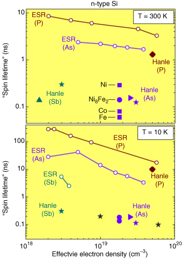
Figure 17.4 Spin lifetime in n-type Si. The spin lifetime is extracted from the Hanle measurements with electrically induced spin accumulation in silicon with different dopants (Sb, As, and P). The electron spin resonance (ESR) markers show data on bulk Si. Reprinted with permission from [49]. The Nature Publishing Group, Copyright 2012
Though spin-MOSFETs have not yet been experimentally verified and there are many important issues to resolve, there has been important progress in increasing spin injection efficiency and observing a relative long spin lifetime. These achievements constitute an existence proof of spin-MOSFET operation at room temperature.
17.2.3 Pseudo-Spin FET
A number of problems associated with high spin injection efficiency into a semiconductor channel have stimulated a search for a hybrid device which would provide the same or similar output characteristics as a spin-MOSFET without the need for a magnetic source and drain. Such a device [referred to as a pseudo-spin-MOSFET (PS-MOSFET)] comprising an ordinary metal oxide semiconductor field-effect transistor (MOSFET) and magnetic tunnel junction has been proposed [53] and experimentally demonstrated [16]. The schematics of the PS-MOSFET are shown in Figure 17.5a. The MTJ is connected to the source of a MOSFET and feeds back its voltage drop to the gate. The degree of negative feedback depends on the resistance states of the MTJ. Thus, there are two possible values for the source–drain current at any fixed bias voltage depending on the magnetic configuration of the MTJ. The prototype PS-MOSFET was built by combining a bottom gate MOSFET and a MTJ with a full Heusler alloy (Co2FeAl; CFA) electrode and an MgO tunnel barrier. The experimentally measured output characteristics of the fabricated PS-MOSFET are shown in Figure 17.5b [54]. The solid and dashed curves show the drain currents for parallel and anti-parallel MTJ configuration, respectively. Each curve follows depletion-type field effect transistor behavior. The drain current is higher for the parallel MTJ configuration over the entire linear and saturation regions. Experimental data in Figure 17.5c show the measured magnetoresistance as a function of Vd for the PS-MOSFET. The results show current-induced magnetization switching (CMIS) among the antiparallel (AP) and parallel (P) states. The obtained output characteristics are similar to the output characteristics simulated for the spin-MOSFET described above [41]. The successful demonstration of the PS-MOSFET has revealed an intriguing possibility of building hybrid logic devices possessing the standard transistor behavior combined with nonvolatility. It is highly expected that the development of PS-MOSFETs will be further elaborated within the next decade by benefiting from the rapid progress in MTJ improvement.

Figure 17.5 (a) Circuit configuration of the pseudo-spin-MOSFET (PS-MOSFET). (b) Experimentally measured output characteristics of the hybrid PS-MOSFET at RT. (c) Measured magneto resistance as a function of Vd for the hybrid integrated PS-MOSFET. The results show current-induced magnetization switching (CMIS) among the antiparallel (AP) and parallel (P) states. Reprinted with permission from [54]. Copyright 2012
17.2.4 Graphene Spintronics
The quest for long spin lifetime has stimulated the study of spin transport in a variety of materials/nano-structures, which may be potentially used in spin-FETs. Here, we would like to refer to the most notable experimental works in this field.
Recently, a great deal of interest has been attracted to the potential utilization of graphene in spin-based devices. The most promising advantage of graphene is a long spin lifetime. According to theoretical predictions [55], spin lifetimes in a single and bilayer graphene sheets may exceed 100 ns at room temperature. Experimentally, a spin life time in the order of 1 ns at room temperature has been observed in both single- and bi-layer graphene [56]. The experimental data show a significant difference in the lifetime dependences for single-layer graphene (SLG) and bilayer graphene (BLG). In SLG, the spin lifetime varies linearly with the momentum scattering time as carrier concentration is varied, while the lifetime in BLG exhibit an inverse dependence [56]. Experimental data on room temperature spin lifetime in bilayer graphene are shown in Figure 17.6, indicating a strong lifetime decrease for samples with higher mobility. The major mechanisms of spin relaxation and the possibility of spin lifetime enhancement are currently under discussion and are currently not well understood.

Figure 17.6 Hanle effect measurements of room temperature spin-relaxation times in a variety of bilayer graphene samples. Reprinted figure with permission from [56]. Copyright 2013 by the American Physical Society
The feasibility of using graphene as a tunneling barrier for MTJ [57] was also studied. The schematics of the device structure of SLG tunneling barrier and experimental data on the tunneling magnetoresistance are shown in Figure 17.7. Transport occurs by quantum tunneling perpendicular to the graphene plane and preserves a net spin polarization of the current from the contact so that the structures exhibit tunneling magnetoresistance to 425 K. These results demonstrate graphene capabilities as an effective tunnel barrier for both charge and spin-based devices. The unique electronic structure of graphene systems can be used to create pseudo-spin analogs of giant magnetoresistance and other established spintronics effects [8].

Figure 17.7 (a) Graphene tunnel junction devices. (b) TMR curves for selected temperatures to 400 K. Reprinted with permission from [57]. Copyright 2013, by the American Chemical Society
Despite the unique physical properties of graphene, its application in spin-based logic devices may be limited due to the following reasons. Low spin–orbit coupling (one of the reasons for long spin lifetime) makes graphene inefficient for spin-FETs. The absence of a bandgap makes the use of graphene channels in MOSFETs problematic because of the high Off current. The observed TMR in MTJ with graphene tunneling layer are orders of magnitude lower than for conventional MTJ with MgO. With all that, the long spin lifetime together with high mobility offered by graphene are most likely to be implemented in logic devices using spin polarized current for nanomagnets switching [58–60], to be discussed later in the text.
17.2.5 Organic Spintronics
The observation of long spin lifetime in organic semiconductors [61,62] has stimulated interest in organic materials as a possible medium to transport and control spin-polarized signals. Organic semiconductors are characterized by very low spin–orbit interaction, which, together with their chemical flexibility and relatively low production costs, makes them a promising materials system for spintronics applications [9]. So far, the most studied organic spintronic device is a spin valve comprising two ferromagnetic electrodes with an organic semiconductor layer in between. The typical thickness of the organic tunneling barrier is several nanometers or less allowing the observation of tunneling magnetoresistance. The first report on vertical injection organic spin valve was published in 2004 showing about 40% TMR at 11 K for (8-hydroxyquinoline)aluminum(III) (Alq3) [63]. Since then, many groups have confirmed similar MR from the devices with the same architecture, using both Alq3 and other OSC materials as a spacer layer (a review is given in Reference [64]). Remarkably, there are many discrepancies in reported results, which may be attributed to intrinsic material properties as well as to the interface quality and fabrication conditions [64,65].
Among the possible advantages offered by the Organic Spintronics is the possibility of building single-molecule spin-based devices. Recently, a giant magnetoresistance of 60% across a single, nonmagnetic hydrogen phthalocyanine molecule H2Pc [66] was observed. The topographic image of the device and experimental data are shown in Figure 17.8. The H2Pc molecules adsorbed onto two cobalt islands on the Cu(111) surface. The obtained I–V spectra clearly show the difference between parallel and anti-parallel oriented cobalt islands. This and other experimental reports [67] show significant progress in making organic spin-based devices.

Figure 17.8 (a) Topographic image of H2Pc molecules adsorbed onto two cobalt islands on the Cu(111) surface. (b) Typical dI/dV spectra taken on parallel and antiparallel oriented cobalt islands [marked by red and blue crosses in (a)]. (c) Energy dependence of the TMR ratio calculated from the dI/dV spectra. Reprinted with permission from [66]. Copyright 2013, Nature Publishing Group
Organic semiconductors are promising for spintronic application due to the long spin lifetime and the ability for efficient spin injection. At the same time, the spin diffusion length in organic semiconductors is limited to a range in the tens of nanometers due to the low mobility of organic crystals. Besides that, molecular spin-based devices are greatly affected by size variations and interface quality. Overall, it is difficult to expect that organic spintronics will provide any robust logic device in the foreseeable future which would be able to compete with CMOS.
17.2.6 Logic Circuits with Spin Transistors and Comparison with CMOS
The unique output characteristics provided by spin transistors opens new possibilities for logic circuit construction. For instance, the oscillation of the output current as a function of the gate voltage in spin-FETs is very useful for realization of specific logic functions such as XOR. At some point, the output characteristics of the device proposed by Datta and Das are similar to the ones of the single-electron transistor (SET) [68] and the logic circuits developed for SETs may be applicable for spin-FETs (e.g., one can compare the XOR circuit with SETs [69] and XOR circuit with spin-FETs [70]). Spin-MOSFETs possess great performance potential for reconfigurable logic by utilizing parallel/antiparallel configurations of source and drain [71]. There has been a growing interest in the MTJ-based nonvolatile logic circuits during the past five years [72–75]. However, the introduction of MTJ has certain side effects which limit the operating speed, reduce variability tolerance and static noise margin. Spin-MOSFETs and PS-MOSFETs may resolve some of the limitations inherent to the MTJ-based logic circuits [76]. Reconfigurable logic circuitry is another potential area of application for spin-MOSFETs and PS-MOSFETs [77]. Logic circuits consisting of spin-MOSFETs can be reprogramed by changing the magnetic configuration of source and drain of the individual transistors. The advantage of this approach is that the magnetization switching, which is a relatively slow process, is required only for reconfiguration, while the speed of operation itself is not limited by the magnetization switching time.
The most important question is whether or not spin transistors can outperform CMOS and provide a higher functional throughput? The optimistic projections predict significant improvement over the scaled CMOS for reconfigurable logic circuits (i.e., 6.8× improvements in delay, 32× active power, and 5.8× in area [71], or about 40% area–delay product improvement [77]). In all cases, the advantages are due to the nonvolatility provided by spin-MOSFETs. It is important to note that the potential improvements are directly related to the practically achievable magneto-current ratio. Figure 17.9 shows the estimates of the potential advantage of area–delay product as a function of the magneto current ratio, MC, defined as MC = (IP − IAP)/IAP where IP and IAP are parallel and antiparallel currents, respectively. In turn, the magneto-current ratio is mainly defined by the spin scattering effects in the channel. Spin scattering generates a large amount of down-spin electrons, which increases the current in the antiparallel configuration, and eventually, degrades the MR ratio. According to the theoretical estimates [78], the MR ratio may exceed 1000 in the ideal channels without scattering, though the experimentally observed values are two orders of magnitude below. In Table 17.1, we summarize the key parameters of the different kinds of spin transistors, their most appealing characteristics, possible logic circuits, projected advantages over CMOS, and their current status of development.

Figure 17.9 Results of numerical simulations: potential advantage of spin-MOSFET FPGA as a function of the magneto current ratio. Reprinted with permission from [77]. Copyright 2013, American Institute of Physics
Table 17.1 Summary of Spin-FETs
| Device/material | Appealing property | Potential logic implementation | Key issue | Level of development |
| Spin-FET | Output current oscillates a s a function of the gate voltage | Complex logic circuits (i.e., XOR) | Requires strong spin–orbit coupling | Prototype operating at 1.8 K [43] |
| Spin-MOSFET | Transistor + built-in memory | Reconfigurable, Nonvolatile circuits | Requires efficient spin injection | Spin injection in Si at RT [50] |
| PS-FET | Transistor + built-in memory | Reconfigurable, Nonvolatile circuits | — | Prototype operating at RT [81] |
| Graphene-based | Long spin lifetime, high mobility | As a channel for spin polarized current | Absence of bandgap | Spin injection in graphene at RT [56] |
| Organic-based | Long spin lifetime | One molecule – one gate, magnetostrictive memory | Short spin diffusion length | Magnetoresistance of 60% [66] |
In summary, spin transistors possess unique output characteristics, which are of potential for particular logic circuits. The oscillating output of the Spin-FET can be used for complex logic circuit construction (i.e., XOR gate) and for reducing the number of elements per circuit. Spin-MOSFETs and PS-FETs combine the characteristics of conventional transistors and a memory element, which can be utilized in nonvolatile and field programmable logic circuits [79,80]. The successful realization of room temperature operating PS-FET [81] brings the development of this device to the next circuit level. It is expected that the introduction of PS-FETs would reduce energy consumption though the use of relatively slow MTJ which would apply some restrictions on the circuit speed. The development of spin FETs may benefit from the advances in the development of novel materials (i.e., graphene- and organic-based spintronics). Table 17.1 summarizes the most appealing properties, key issues, and the level of development of Spin-FETs.
17.3 Magnetic Logic Circuits
Another (transistor-less) approach to spin-based logic devices is by exploiting magnetization as a state variable. Within this approach, logic 0 and 1 are assigned to the two ground states of the nanomagnet (i.e., magnetization along or opposite to the easy-axis) and logic functionality is associated with the switching among these states. Similar to electronic transistor-based circuits, where one transistor drives the next stage transistors by an electric field, magnetic logic circuits requires one magnet to drive next stage magnets by providing a magnetic field. There are different possible ways to interconnect the input and the output magnets (e.g., by making an array of nanomagnets sequentially switched in a domino fashion [20], by sending a spin polarized current [59], by sending a spin wave [82], or by moving a domain wall [83]). In this section, we describe the principle of operation of different magnetic logic circuits and discuss their potential advantages and drawbacks.
17.3.1 NanoMagnetic Logic
The nanomagnet logic (NML) is a variant of the edge-driven, quantum-dot cellular automata (QCA) architecture aimed to benefit from the local coupling among nano-cells. This concept was originally proposed for the electron-based cellular structure, where an elementary cell consists of four quantum dots, with two excess electrons that can tunnel between the dots tending to occupy diagonally opposite dots due to Coulomb repulsion [84]. The electronic version of QCA appeared to be impractical, like many other single-electron logic devices due to their great sensitivity to the inevitable size variations. This issue is addressed in the magnetic version of QCA (MQCA) [85], where an elementary cell is represented by a nanomagnet of a certain shape and material to exhibit a single domain behavior. When they are connected via strong exchange interaction, the spins of the nanomagnet show collective behavior, which is much more immune to structure variation than a single electron. Later, the concept of MQCA-NML has evolved in a number of works [86–90].
Logic “0” and “1” in NML are assigned to the two ground states of the nanomagnet (i.e., magnetization along or opposite to the easy-axis). Information transfer within the NML is accomplished via dipolar coupling among nearest-neighbor nanomagnets. An example of a nanomagnetic wire is shown in Figure 17.10. It is formed from a line of permalloy islands (70 × 135 nm) separated by an air gap of 25 nm. The nanomagnets are anti-ferromagnetically ordered due to the strong dipolar interaction. The operation of NML logic gates requires a clock magnetic field to modulate the barrier between magnetization states of the coupled nanomagnets. The clocking field can be applied along the hard axis of the nanomagnets as illustrated in Figure 17.10d [91]. The initial configuration is one of two collective ground states for the line of the dipole–dipole coupled magnets. Then, an external magnetic field is applied turning the magnetic moments of the nanomagnets horizontally into a neutral logic state (“null state”) against the preferred magnetic anisotropy (i.e., along the hard axes of the magnets). When the field is removed, the nanomagnets relax into the anti-ferromagnetically ordered ground state, as illustrated in Figure 17.10d. If the first magnet of the chain is influenced by an input device during relaxation, it will set the state of the whole chain via dipole–dipole interaction.

Figure 17.10 (a)Scanning electron microscope (SEM) image of a chain of 16 permalloy nanomagnets (70 × 135 nm, thickness 30 nm). (b) MFM image of the same chain shows alternating magnetization of the magnets as set by the state of the horizontal driver magnet (circled). (c) SEM image of functioning majority gate. (d) How clock works. Reprinted with permission from [93]. © 2013 IEEE
Logic functionality in the NML circuit is achieved via the specific geometric configuration of the nanomagnets. The structure of the three-input one-output majority gate is shown in Figure 17.11. The nanomagnets are arranged in two intersecting lines, such that the dipole coupling of the nanomagnets produces ferromagnetic ordering along the vertical line and antiferromagnetic ordering along the horizontal line. The nanomagnets are arranged to provide same-strength coupling to the central nanomagnet, which switches to the state corresponding to the majority of inputs. The MFM images of two possible input logic combinations are shown in Figure 17.11b–c. Such a majority gate can be reduced to a reconfigurable two-input AND/OR gate by setting the third input to a logic “0” or “1” (i.e., the MAJ gate operates as an AND gate if the third input is set to 0, and the same gate operates as an OR gate if the third input is set to 1). The NOT gate in NML comprises just two anti-ferromagnetically coupled nanomagnets, as the two magnets tend to be magnetized in the opposite directions corresponding to the 01 or 10 logic states. Figure 17.12 shows a recently reported NML fan-out (1 : 3) structure with gain provided by a magnetic clocking field. All other Boolean logic gates in NML can be built via Majority gates and Inverters.
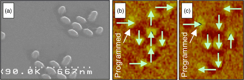
Figure 17.11 (a) SEM image of majority gates with long inputs. (b) and (c) MFM images of majority gate with “programmed” input. Reprinted with permission from [93]. © 2013 IEEE

Figure 17.12 (a) SEM image of an NML ensembles one that serves as a fanout structure. (b) MFM image showing fanout operation. Reprinted with permission from [93]. © 2013 IEEE
During the past five years, there has been significant progress in NML component development and experimental demonstration [89]. A summary for the experimentally demonstrated logic gates is presented in Table 17.2.
Table 17.2 Experimentally demonstrated NM logic circuits (all gates operate at room temperature)
| Logic gate comment/Reference | Clock wire height/width/length (μm) | Magnetic field generating current (mA) | Structure footprint (nm) | Energy with 25 μs pulse time (nJ) | Energy with 10 μs pulse time (pJ) |
| Magneta [92] | 2.4/1.5/500 | 680 | 60 × 90 | 0.388 | 0.155 |
| NM lineb [93] | 2.8/1.4/500 | 600 | 60 × 90 × N | 0.397 × N | 0.159 × N |
| Two-input AND and OR gatec [93] | 2.8/1.4/500 | 850 | 440 × 220 | 8.03 | 3.21 |
| One-bit adderb,d [94,95] | 2.8/1.4/500 | 760 |
Half-adder: 780 × 230 Carry gate: 320 × 230 |
11.2 | 4.47 |
| aMagnets switched along easy axis which would not be done for clocking. | |||||
| b(1) Higher currents/fields needed because input driver must be switched along easy axis; (2) experiments were done on a five-magnet wire, energy listed per magnet; (3) to apply current pulses, audio amplifier used in experiments which gave rise to 25 μs pulse time, this energy is reported (along with a more reasonable 10 ns pulse time); (4) assumes 50% clock wire coverage. | |||||
| c(1) Higher currents/fields needed because input driver must be switched along easy axis; (2) assumes gate comprised of ∼ 5 magnets; (3) to apply current pulses, audio amplifier used in experiments which gave rise to 25 μs pulse time – this energy is reported (along with a more reasonable 10 ns pulse time); (4) assumes 67% clock wire coverage. | |||||
| d(1) Energy projections based on clock experiments of lines and gate summarized above; adder experiments were done with external field; (2) assumes 100% coverage. | |||||
Besides that, a great deal of efforts has focused on the NML circuits modeling and application-oriented architecture development [93,96–100]. The benchmarks on the circuit area, internal delay, energy per operation, and functional throughput are shown in Table 17.2. The estimates are shown for MAJ gate, which is the base block for NM logic. The area per circuit is shown in the characteristic lithography size (DRAM's half-pitch) F. Only internal delay is taken into consideration, and the energy per operation is shown without the energy required for the clock.
Energetically efficient clocking, magneto-electric interface, and fault tolerance are the key technological issues to be addressed. As of today, all of the reported NML prototypes were clocked by the external magnetic field produced by the electric current in the conducting contours (i.e., laboratory electromagnets). Energy losses in the magnetic field generating contours may significantly exceed the internal losses within the NML circuit. According to numerical estimates [101], the Joule heat losses in a conducting loop of resistance 10 ohms, generating a 267 Oe magnetic field for magnetization reversal in a 105 × 95 × 6 nm nanomagnet made of nickel will exceed 1.5 pJ. Thus, the energy losses of a single element may be 1000 times larger than the energy dissipated within the complete circuit (i.e., compare to the projected energy per operation in MAJ gate; Table 17.3). A similar problem arises for the magneto-electric interface. The input magnets in the NML circuits should be individually addressed to convert input electrical signal in the magnetization state (i.e., via spin transfer torque). The energy per switch in this case is also of the order of 0.5 pJ [101].
Table 17.3 Estimates on NML MAJ gate
| MAJ gate | Benchmark (F = 15 nm) |
| Circuit area (64F2) | 0.0144 μm2 |
| Internal delay | 400 ps |
| Energy per operation (w/o clock) | 19.31 aJ |
| Functional throughput | 2.51 Pops s−1 cm−2 |
There are two major causes of errors in NML: static faults due to the manufacturing defects (e.g., magnet misalignment [102]) and dynamic faults due to the thermal noise. Both causes are most critical during the switching process when the nanomagnets relax from the “null” to the final state. This problem can be addressed by introducing nanomagnets with a magnetocrystalline biaxial anisotropy, which can be used to introduce a local energy minimum and to increase hard axis stability [103]. Fault tolerance can also be enhanced via adiabatic switching and/or field gradients [89]. The feasibility of building error-tolerant NML circuits is currently debated [89,101].
Overall, NML is one of the most explored approaches in the area of Spintronic Logic. NML logic gates (i.e., Inverters, Buffer lines, MAJ gates) have been experimentally demonstrated at room temperature [87]. It is expected that NML will continue to advance and more prototypes (i.e., two-bit Adder circuit) will be experimentally demonstrated within the next two years. Scalability and low power consumption are the main appealing properties of the NML approach, promising an overall power-performance advantage over the scaled CMOS. NML logic circuits might be employed for Boolean (systolic arrays) as well as for nonBoolean information processing [98,104]. The main technological issues of NML are associated with the circuit reliability and defect tolerance [105]. Thermal noise and fabrication-related imperfections can cause errors in signal transmission and logic function in NML circuits [106]. A more detailed description and analysis of NML logic will be given in Chapter 22.
17.3.2 All Spin Logic
The communication between the input and output nanomagnets can be accomplished via spin polarized currents [58]. Within this approach, nanomagnets share a common spin-coherent channel. Some of the magnets have fixed magnetization and some of them can be switched due to the spin torque produced by the spin polarized current. This approach has been further evolved in the All Spin Logic (ASL) [59]. The basic concept of switching in ASL is illustrated in Figure 17.13. There are shown two elementary magnetic cells connected via a spin-coherent channel. The cell comprises from the top to the bottom the following: metallic contact; magnetic free layer, and a tunneling layer. It is assumed that the free layer has two thermally stable magnetic configurations and can be used as a built-in memory. The cells communicate via a spin-polarized current propagating through the channel. In order to switch the cell on the right side, the cell on the left side generates a spin polarized current which flows through the channel and provides a torque on the magnetization of the output cell. There are two possible switching scenarios, as described in [59]: (i) the magnetization of the free layer of the output cell is switched if the strength of the torque exceeds certain threshold value; (ii) a supply voltage is applied to the output cell driving the magnetization of the free layer of the output cell in a metastable state. Then, the torque provided by the current defines the relaxation direction towards one of the two stable states. The use of voltage-assisted switching has certain advantages and allows for significant reduction of the spin polarized current required for switching, as the strength of the torque has to be just above the noise level in order to define the final state. There are several possible layouts for constructing cascadable ASL gates [59]. Shown in Figure 17.14, is an example of a circuit comprising two gates (four cells per gate). Each of the gates can function as a NAND/NOR or AND/OR gate. A variety of Boolean logic gates can be constructed by implementing different channel configurations and clocking schemes. The channel in ASL has to provide maximum spin coherence and can be made of semiconductors as well as metallic materials. Graphene may be the best candidate for application in ASL as it combines long coherence length with high mobility. Magnetologic gates with a hybrid graphene/ferromagnet material system have been recently proposed [60].

Figure 17.13 Schematics of the ASL switch. Two magnetic cells share the common spin-coherent channel. Logic 0 and 1 are assigned to the magnetic state of the free layer (1) of the cell. The cells communicate via the spin polarized current in the channel (4). Reprinted with permission from [59]. Copyright 2013, Nature Publishing Group

Figure 17.14 Possible layout for cascadable ASL circuit. The state of the output is determined by the spin currents injected in the channel by the inputs. Signal propagation is controlled by the voltage applied to the individual cells. Reprinted with permission from [59]. Copyright 2013, Nature Publishing Group
The ASL approach is free of constraints inherent to the schemes using dipole–dipole coupling and allows for much higher defect tolerance as the variations in the position of the elementary cells is of minor importance. It is also scalable since shorter distances between the input/output cells require less spin polarized currents for switching. The use of voltage-assisted switching may be an efficient amplification mechanism, taking energy from the conventional voltage supply. According to the theoretical estimates [107], ASL can potentially reduce the switching energy–delay product. The major issues of this scheme are associated with the electrical isolation among the electrically biased cells and the realization of the spin-coherent channel. It is desired to have spin-polarized currents flowing only between the input and the output cells though the potential difference may arise among the output cells or the cells of the different stages. No working ASL circuits have been prototyped to date.
17.3.3 Spin Wave Devices
Spin Wave Devices (SWD) are a type of magnetic logic exploiting collective spin oscillation (spin waves) for information transmission and processing [108,109]. The schematics of the SWD logic gate are shown in Figure 17.15. The circuit consists of: (i) magneto-electric cells, (ii) magnetic waveguides – spin wave buses, and (iii) a phase shifter. The magneto-electric cell (ME cell) is the element used to convert voltage pulses into the spin waves as well as to read out the voltages produced by the spin waves. The operation of the ME cell is based on the effect of magneto-electric coupling in multiferroics enabling magnetization control by applying an electric field and vice versa [82]. The principle of operation is the following. SWD receives initial information in the form of voltage pulses (e.g., +10 mV corresponds to logic state 0, and −10 mV corresponds to logic state 1). The polarity of the applied voltage defines the initial phase of the spin wave signal (e.g., positive voltage results in clockwise magnetization rotation and negative voltage results in counter clockwise magnetization rotation). Thus, the input information is translated into the phase of the excited wave (e.g., initial phase 0 corresponds to logic state 0, and initial phase π corresponds to logic state 1). Then, the waves propagate through the magnetic waveguides and interfere at the point of waveguide junction. For any junction with an odd number of interfering waves, there is a transmitted wave with a nonzero amplitude. The phase of the wave passing through the junction always corresponds to the majority of the phases of the interfering waves (e.g., the transmitted wave will have phase 0, if there are two or three waves with initial phase 0; otherwise, the wave will have a π-phase). As the transmitted wave passes the phase shifter, it accumulates an additional π-phase shift (e.g., phase 0 → π, and phase π → 0). Finally, the spin wave signal reaches the output ME cell. The output cell has two stable magnetization states. At the moment of spin wave arrival, the output cell is in the metastable state (magnetization is along the hard axis perpendicular to the two stable states). The phase of the incoming spin wave defines the direction of the magnetization relaxation in the output cell [82,109]. The process of magnetization change in the output ME cell is associated with the change of electrical polarization in the multiferroic material and recognized by the induced voltage across the ME cell (e.g., +10 mV corresponds to logic state 0, and −10 mV corresponds to logic state 1).

Figure 17.15 Schematic view of the SWD logic circuit. There are three inputs (A,B,C) and the output D. The inputs and the output are the ME cells connected via the ferromagnetic waveguides – spin wave buses. The input cells generate spin waves of the same amplitude with initial phase 0 or π, corresponding to logic 0 and 1, respectively. The waves propagate through the waveguides and interfere at the point of junction. The phase of the wave passed the junction corresponds to the majority of the interfering waves. The phase of the transmitted wave is inverted (e.g., passing the domain wall). The table illustrates the data processing in the phase space. The phase of the transmitted wave defines the final magnetization of the output ME cell D. The circuit can operate as a NAND or NOR gate for inputs A and B depending the third input C (NOR if C = 1, NAND if C = 0). Reprinted with permission from [115]. Copyright 2013, American Institute of Physics
The operation of the SWDs is based on the spin wave interference, which provides the mechanism for phase-based data processing. During the past five years, three- and four-terminal SWDs exploiting spin wave interference have been experimentally demonstrated [110,111]. Figure 17.16a shows the top view of the four-terminal SWD. The sample consists of a silicon substrate, a 20 nm layer of Ni81Fe19, a 300 nm layer of silicon dioxide, and a set of five conducting wires on top. The distance between the wires is 2 μm. Three of the five wires are used as input ports, and the two other wires are connected in a loop to detect the inductive voltage produced by the spin wave interference. The direction of the current in the wires defines the phase difference between the excited spin waves (i.e., the waves have the same initial phase if the direction of the current is the same direction, and there is a π-phase difference if the current flows in the opposite direction). The plot in Figure 17.16b shows the output inductive voltage for different combinations of spin wave phases. The blue and red curves correspond to the case when all three waves are excited in phase, and the black and green curves correspond to the case when one of the waves has a π-phase difference with the others. The experimental data show the change of the phase of the output voltage as a function of the input combination (i.e., 000, π00, 0π0, 00π corresponds to the output phase 0, and πππ, 0ππ, π0π, ππ0 results in the change of the output phase voltage of π). This logic device operates as MAJ gate in the phase space. The data are taken at 95 Oe bias magnetic field (perpendicular to the spin wave propagation), 3 GHz frequency, and at room temperature.
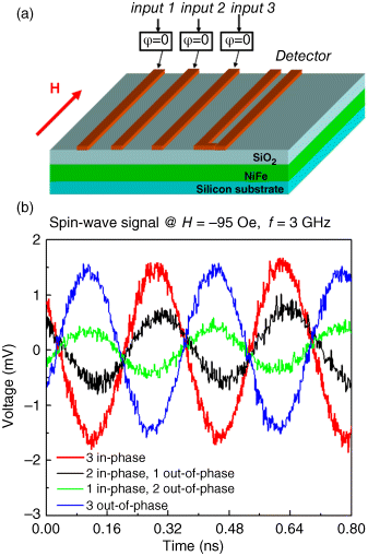
Figure 17.16 (a) Schematics of the four-terminal SWD. The device structure comprises a silicon substrate, a 20 nm layer of permalloy, a layer of silicon dioxide, and a set of five conducting wires on top (three wires to excite three spin waves, and the other two wires connected in a loop are to detect the inductive voltage). The initial phase of the excited spin wave (0 or π) is controlled by the direction of the excitation current. (b) Experimental data showing the inductive voltage as a function of time. The curves of different colors correspond to the different combinations of the phases of the interfering spin waves. Reprinted with permission from [115]
The use of electric current wires for spin wave excitation appeared to be energetically inefficient (i.e., >pJ per spin wave), as only a small amount of energy is transferred into the spin wave. It would be much more efficient to utilize multiferroics for energy conversion between the electric and magnetic domains [112]. Recently, spin wave excitation and detection by synthetic multiferroic elements was experimentally demonstrated [113]. The schematics of the experiment and experimental data are shown in Figure 17.17. Two synthetic multiferroic elements were used to excite and detect a spin wave propagating in the permalloy waveguide (the distance among the excitation and the detection elements is 40 μm). The multiferroic element comprises a layer of piezoelectric (PZT) and a magnetostrictive material (Ni). An electric field applied across the piezoelectric produces stress, which, in turn, affects the magnetization of the magnetostrictive material. Thus, the applying of AC voltage to the multiferroic element results in magnetization oscillation (a spin wave). Vice versa, a change of magnetization in the magnetostrictive layer results in a voltage signal due to the produced stress. The experimental data in Figure 17.17b show the collection of data obtained at different operational frequencies and bias magnetic field. The utilization of multiferroics has resulted in the energy reduction to about 10 fJ per wave [113]. The major characteristics of the experimentally demonstrated SWD prototypes are summarized in Table 17.4.
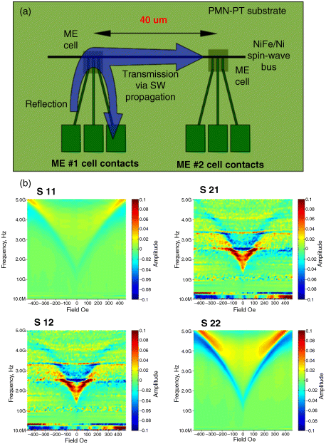
Figure 17.17 (a) Schematics of the experiment on spin wave excitation and detection by multiferroic elements (ME cells). (b) Collection of the experimental data (S11, S12, S21, and S22 parameters) obtained at different frequencies and bias magnetic field. Reprinted with permission from [113]
Table 17.4 Experimentally demonstrated SWDs (all devices operate at room temperature)
| Logic gate comment/Reference | Circuit size width/length (μm) | Operational frequency (GHz) | Signal/noise ratio | Energy per wave |
| Three-terminal SWD [110] | 700/12 | 0.5–3.0 | 2 (maximum) | >10 pJ |
| Four-terminal SWD (MAJ gate) [111] | 500/24 | 3.0 | ∼10 (average) | ∼pJ |
| Two-terminal line with ME cellsa [113,114] | 500/40 | 0.5–5.0 | N/A | 10 fJ |
| aThe energy per wave has been estimated based on the excitation conditions. | ||||
The expected advantages of SWD technology include: (i) the ability to utilize phase in addition to amplitude for building logic devices with a smaller number of elements than required for transistor-based approach [82], and (ii) parallel data processing on multiple frequencies at the same device structure by exploiting each frequency as a distinct information channel [115]. Wave-based magnonic logic devices may complement CMOS in special task data processing (i.e., image processing), by exploiting wave interference for functional throughput enhancement. The major issues of SDW approach include the problems with energetically efficient spin wave excitation and detection, fast attenuation time (∼1 ns at RT), and spin wave dispersion [102]. All of the demonstrated prototypes utilize spin waves of micrometer scale wavelength, which makes them immune with respect to the waveguide structure imperfections. It is not clear if scaling to the deep sub-micrometer range would significantly affect the signal to noise ratio as well as the speed of propagation. At some point, the success of the SWD approach depends on the ability to detect and amplify spin waves (i.e., by multiferroic elements or spin torque oscillators), which can enhance SWD noise immunity.
17.3.4 Hybrid Spintronics and Straintronics Devices
A new approach to magnetization control via applied stress was recently proposed and became known as Hybrid Spintronics and Straintronics [116,117]. The essence of this approach is in the use of two-phase composite multiferroics comprising piezoelectric and magnetostrictive materials, where an electric field applied across the piezoelectric produces stress, which, in turn, affects the magnetization of the magnetoelastic material. Although work in this area can be traced back to the 1970s [118], composite multiferroics have been in a shadow of single-phase multiferroics (i.e., BiFeO3 and its derivatives [119]) for a long time. The recent resurgence of interest in composite multiferroics is due to the technological flexibility, where each phase (piezoelectric or magnetostrictive) may be independently optimized for room temperature performance. More importantly, the strength of the electro-magnetic coupling in the two-phase systems can significantly exceed the limits of the single-phase counterparts [120]. During the past two years, there have been several experimental works showing magnetization rotation in two-phase multiferroics as a function of the applied voltage [117,121]. For instance, a reversible and permanent magnetic anisotropy reorientation was reported in a magnetoelectric polycrystalline Ni thin film and (011)-oriented [Pb(Mg1/3Nb2/3)O3](1−x)−[PbTiO3]x heterostructure [117]. An important feature of the magneto-electric coupling is that the changes in magnetization states are stable without the application of an electric field and can be reversibly switched by an electric field near a critical value (i.e., 0.6 MV/m for Ni/PMN-PT). Such a relatively weak electric field promises the ultra-low energy consumption required for magnetization switching [122]. The estimates of power dissipation in a two-phase multiferroic material are shown in Figure 17.18 [116]. The dissipated energy is calculated as follows:
where C is the capacitance of the multiferroic element, which is defined by the dielectric properties of the piezoelectric layer, and the dimensions of the element, V is the voltage needed to generate the stress sufficient for magnetization reversal, and Ed is the energy dissipated in the nanomagnet due to Gilbert damping [116]. The voltage required for magnetization switching can be found by solving the Landau–Lifshitz–Gilbert (LLG) equation for particular materials or estimated, based on experimental data. The estimates predict values as low as tens of kT energy dissipated per switch at a nanosecond switching time. For example, the total energy dissipated is 45 kT for a delay of 100 ns and 70 kT for a delay of 10 ns. It is important to note that, according to the theoretical estimates [116], the energy dissipation increases sub-linearly with the switching speed. For example, in order to increase the switching speed by a factor of 10, the dissipation needs to increase by a factor of 1.6.

Figure 17.18 Numerical estimates on the energy dissipated in the circuit with multiferroic nanomagnets as functions of delay for three different materials used as the magnetostrictive layer in the multiferroic nanomagnet. Reprinted with permission from [116]. Copyright 2013, American Institute of Physics
The ability to control magnetization by an electric field presents great potential for application of two-phase multiferroics in magnetic logic devices. Specifically, these elements may resolve the shortcoming associated with input–output isolation in the dipole-coupled NML circuits described in the previous section. In contrast to the global magnetic field provided by the electric current carrying wires, a multiferroic element allows for more local magnetization control. At the same time, stress-mediated electro-magnetic coupling eliminates the problem of the stray field. Another potential benefit of multiferroics is the possibility of building multi-state logic circuits by exploiting the biaxial magnetocrystalline anisotropy of the magnetoelastic material. An example of the four-state universal logic gate (NOR) using a linear array of three dipole-coupled magnetostrictive-piezoelectric multiferroic nanomagnets is described in Reference [123]. Similar ideas for using electric field-controlled nanomagnets can be implemented in other types of logic circuits (i.e., developed for NML).
It is expected that the development of multiferroic elements exploiting stress for magnetization switching will be intensively studied within the next two years and the estimates on ultra-low power dissipation will be experimentally validated. Another important question to be answered is whether or not stress-based multiferroic devices are capable of fast (GHz frequency range) switching.
17.3.5 Spin Torque-based Devices
The discovery of the spin torque effect [124] has resulted in the development of novel mechanism for magnetization switching, which has been successfully implemented in magnetic memory [125]. Spin torque devices (STD) comprise a stack of metallic ferromagnetic layers separated by the tunneling barrier. Passing electric current across the structure produces a spin torque affecting the magnetization of the ferromagnetic layers. Spin torque may result in the oscillation of magnetization (spin wave generation) or complete magnetization reversal of the one of the magnetic layer (i.e., the free layer) when the current density exceeds a certain threshold value. The fabrication technology is fully compatible with CMOS, which makes the spin torque device (STD) a promising candidate for implementation in logic circuits. There are two major approaches to spin torque-based devices: (i) digital devices, where logic states 0 and 1 are encoded into the magnetic state of the free layer(s) [83,126]; (ii) analog devices where logic state is associated with the frequency of the magnetic oscillation.
The schematics of the digital spin torque majority gate (STMG) are shown in Figure 17.19 [83]. There are four STD nanopillars connected via the common ferromagnetic layer. Three of the nanopillars (A, B, C in Figure 17.19) are used as the input gates, and the fourth nanopilalr (Out) is the output gate. Each of the input nanopillars and the output nanopillar has separate fixed layers which are pinned by the antiferromagnetic layers on top of them. Logic input is defined by the polarity of the voltage applied to the input gates (i.e., positive voltage corresponds to logic 1, and negative voltage corresponds to logic 0. The polarity of the applied voltage determines the direction of the spin torque affecting the magnetization of the common free ferromagnetic layer below the nanopillars. Thus, positive voltage forces the magnetization in the free layer to align parallel with the magnetization of the fixed layer, and negative voltage forces the magnetization to align in the opposite direction. As a result of the interplay between the three torque forces, the magnetization of the free layer changes according to the majority of the inputs. The numerical simulations in Figure 17.19 illustrate the process of magnetization change (domain wall motion) in the common layer. The input voltages are applied until the domain wall reaches the output cell. Once the direction of magnetization in the free layer reaches its steady-state configuration, the input voltages are turned off and the results of computation is stored in the magnetization state of the common layer. The read-out is accomplished by sensing the resistance across the output nanopillar (i.e., high resistance corresponds to logic 1 and low resistance corresponds to logic 0).

Figure 17.19 (a) Scheme of the cross section of the MAJ gate consisting of four STDs. The triangles designate the magnetization direction of the free layers. (b) Schematic of the top view of the MAJ gate. The squares designated by “A,” “B,” and “C” are input nanopillars. The square designated by “Out” is the output nanopillar. (c) Results of numerical simulations: several snapshots showing the magnetization of the common ferromagnetic layer. Red color denotes the out-of-plane projection of magnetization pointing up, and blue denotes that pointing down. Reprinted with permission from [83]. © 2013 IEEE
This approach looks very feasible from the technological point of view, as the material structure of the nanopillars in MAJ gate is similar to that in a typical magnetic tunnel junction [127]. The only technological challenge is associated with the electrical isolation of the STDs to prevent unnecessary electric currents, which can be possible resolved by utilizing a nonconducting ferromagnetic layer. The projected potential advantages over the CMOS are in are smaller area, low power, nonvolatility, reconfigurability, and radiation hardness [83]. The estimates on a full adder circuit built of STDs from Ref. [128] are shown in Table 17.5.
Table 17.5 Performance estimates of a full adder circuit with STMGs
| Full adder with STMGs | Benchmark (F = 22 nm) |
| Gate area | 0.13 μm2 |
| Switching time | 2826 ps |
| Switching energy with external circuit | 257 680 aJ |
| Power per gate, active | 45.6 μW |
| Power per gate, standby | 0.0 μW |
| Functional throughput | 1.3 Mops ns−1 cm−2 |
There are a few factors beneficial for STDs circuit. It has a higher density than CMOS, because 28 transistors are replaced by three majority gates. The STDs circuit has lower active power and zero standby power. At the same time, the use of domain wall motion for STD coupling would limit the switching speed and the switching energy. The efficiency of the STD devices is mainly defined by the magnitude of the electric current required for magnetization switching. So far, the best experimental results show about MA/cm2 critical current density (CoFeB free layer [129]). On the one hand, the critical switching current is proportional to the device area and can be scaled down for nanometer size structures. On the other hand, there are certain limits on the size of the free layer to be switched (i.e., due to the thermal stability requirements), which would further restrict the minimum switching current. All these fundamental issues could narrow the potential applications of the domain wall-coupled STDs.
Another approach to STD coupling is via spin waves [130]. This approach is based on the property of nanometer scale spin torque devices generate spin waves in response to a d.c. electrical current [131,132]. Electric current passing through a spin torque nano-oscillator (STNO) generates spin transfer torque and induces auto-oscillatory precession of the magnetic moment of the spin valve free layer. The frequency of the precessing magnetization is tunable by the applied dc voltage due to the strong nonlinearity of the STNO. In case of two or more STNOs sharing a common free layer, the oscillations can be frequency and phase locked via the spin wave exchange [130,133]. Figure 17.20 shows the schematics of the devices with two STNOs (marked as A and B) and the experimental data illustrating the coupling. Figure 17.20c–d plots the evolution of the combined spectrum from both STNOs as current through contact B increases. The phase-locked state is characterized by a narrowing of the signal linewidth (Figure 17.20d) as the current exceed the threshold value. This phenomenon gives rise to the proposal on the logic devices based on coupled STNOs [134]. A majority logic gate based on phase locking of STNOs consists of a common free-layer metallic ferromagnetic nanowire on a metallic nonmagnetic bottom lead with several GMR or TMR junctions patterned on top of the free layer as shown in Figure 17.21. One of these junctions can serve as the gate output while the rest of the junctions are the gate inputs. All inputs are dc current-biased at a current level above the critical current for magnetization self-oscillations. To each input, signals of two frequencies f1 and f2 can be applied. Due to injection locking and spin wave interaction in the common free layer, the entire free layer precesses at either f1 or f2, depending on the input signal frequency applied to the majority of the inputs. Therefore, the output frequency of this logic gate is determined by the frequency applied to the majority of the input gates, and the device operates as a majority logic gate with the signal frequency as the state variable [135].

Figure 17.20 (a) Cross-sectional diagram of two STOs with a common free layer. (b) Micrograph of actual two nano-contact device with two independent leads. (c) Combined spectrum with current density below phase locking. (d) Combined spectrum with phase locking. Reprinted with permission from [130]. Copyright 2013, Nature Publishing Group

Figure 17.21 Schematics of the STO-based MAJ logic gate consisting of a metallic ferromagnetic nanowire with several injectors of spin polarized current (spin toque oscillators with a common free layer). The input frequencies (e.g., f1, f2, f3) assume binary values. The output frequency fout in the phase locking regime is determined by the majority of the input frequencies. Reprinted with permission from [135]
The unique properties of STDs are of great promise for future implementation. Being compatible with CMOS, STDs may serve as complementary logic units for general and special task data processing. The main challenge for the STD approach is to reduce the current required for switching and minimize active power consumption.
17.3.6 Current Status and Perspectives of Magnetic Logic Devices
In summary, magnetic devices provide an alternative approach to logic circuit construction by exploiting intrinsic nonlinearity of magnetic materials. In contrast to Spin-FETs, most magnetic devices do not require high-efficiency spin injection, and a number of room temperature operating prototypes has been demonstrated. Nonvolatility is the main advantage inherent to all schemes, which may potentially eliminate static power consumption. The future success of magnetic logic is mainly related to finding an energetically efficient mechanism for local magnetization control. Development and utilization of multiferroic materials is one of the promising approaches able to scale down energy per magnetization reversal to the atto Joule level. At the same time, the use of nanomagnets for information storage implies certain limits on the operational speed, which is restricted by the time required for magnetization reversal. It is unlikely that magnetic devices will be ever able to compete with CMOS in speed. Nevertheless, magnetic logic circuits can provide higher functional throughput or perform the same data processing tasks with lower energy consumption than CMOS by implementing complex logic functions and/or reconfigurability. For example, NML and ASL circuits are especially suited for adder and multiplier circuits as a part of arithmetic logic units (ALU). SWDs are most efficient for MAJ gate construction by exploiting wave interference and may be also promising for parallel data processing. STDs offer a variety of possible applications including nonvolatile digital circuits (i.e., MAJ gates) and analog dynamical phase-locking system for neuromorphic-type architectures. In Table 17.6, we summarize the most appealing properties, key issues, and the level of development of magnetic logic devices.
Table 17.6 Summary of magnetic logic devices
| Device | Coupling mechanism | Appealing property | Potential application | Key issue(s) | Level of development |
| NML | Dipole–dipole interaction | Nonvolatile | Digital circuits, adders, multipliers | Fault tolerance, energetically efficient clocking | Buffer, AND, OR, one-bit adder prototypes operating at RT [92,93,95] |
| ASL | Spin polarized current | Nonvolatile | Digital circuits, adder, multiplier circuits | Spin-coherent channel, input–output electric isolation | Numerical modeling [59] |
| SWD | Spin waves | Utilizes interference for data processing | Parallel data processing | Efficient mechanism for wave excitation, dispersion. | MAJ gate prototype operating at RT [121,122] |
| STD | Domain wall movement; spin waves | Noise immunity | CNN architectures | Electrical isolation | Two-coupled STNOs [133] |
17.4 Summary
Adding the spin degree of freedom to conventional charge-based electronic devices appears to be a nontrivial task. So far, the tremendous efforts to exploit spin–orbit coupling for current modulation in spin-FETs have resulted in a low-temperature (1.8 K) operating prototype [43]. The attempt of building FETs without relying on spin–orbit coupling (spin-MOSFETs) has faced another grand challenge – the need for efficient spin injection. Currently, both spin-FETs and spin-MOSFETs are far from competing with CMOS technology. More encouraging is the progress in pseudo-spin FETs [54], showing the possibility of building hybrid logic devices possessing standard transistor behavior combined with nonvolatility. However, the integration of relatively slow MTJ with a scaled CMOS has certain architecture restrictions and speed-energy tradeoffs. The development of novel materials and nanostructures with long spin lifetime may further benefit the development of spin-FETs.
The idea of using spin (collection of spins) alone has resulted in a number of proposals, as described in this chapter. The principle of operation of magnetic logic devices is fundamentally different from the conventional transistor-based approach. On the one hand, the unique output characteristics of magnetic devices promise additional functionalities beyond the capabilities of the conventional FET. On the other hand, the integration of spin-based devices with conventional electron-based devices introduces a significant problem. During the past five years, there has been a continuous progress in the development of magnetic logic devices. Several room temperature operating prototypes have been demonstrated (e.g., see Table 17.4). The further development of magnetic logic is expected to show examples of specific logic gates exploiting the unique output characteristics of magnetic devices. The main challenges include the development of energetically efficient clocking, reliable magnetic interconnects, and an electro-magnetic interface for integration within the chip. The development of spin transfer- and multiferroic-based devices may significantly improve the energetic efficiency of magnetic logic. Though magnetic devices cannot complete with CMOS in speed, they hold the promise of nonvolatile and reconfigurable logic, which may provide some functional enhancement at reduced power consumption (assessment and benchmarking are presented in Chapter 21).
Overall, in spite of great efforts and research activities, spin-based logic circuitry remains in its infancy. It is very unlikely that spin-based logic devices will be able to compete with CMOS circuitry in all figures of merit. However, the unique output characteristics of magnetic devices may find applications in specific circuits and architectures aimed not to replace but to complement CMOS in special data processing tasks.
References
- 1. Prinz, G.A. (1998) Device physics – magnetoelectronics. Science, 282, 1660–1663.
- 2. Wolf, S.A. et al. (2001) Spintronics: A spin-based electronics vision for the future. Science, 294, 1488–1495.
- 3. Johnson, M. and Silsbee, R.H. (1985) Interfacial charge-spin coupling – injection and detection of spin magnetization in metals. Physical Review Letters, 55, 1790–1793.
- 4. Baibich, M.N. et al. (1988) Giant magnetoresistance of (001)FE/(001) CR magnetic superlattices. Physical Review Letters, 61, 2472–2475.
- 5. Binasch, G. et al. (1989) Enhanced magnetoresistance in layered magnetic-structures with antiferromagnetic interlayer exchange. Physical Review B, 39, 4828–4830.
- 6. Wolf, S.A. et al. (2006) Spintronics – A retrospective and perspective. Ibm Journal of Research and Development, 50, 101–110.
- 7. Slonczewski, J.C. (1996) Spintronics and spin transfer torque. Journal of Magnetism and Magnetic Materials, 159, L1–L7.
- 8. Pesin, D. and MacDonald, A.H. (2012) Spintronics and pseudospintronics in graphene and topological insulators. Nature Materials, 11, 409–416.
- 9. Dediu, V.A. et al. (2009) Spin routes in organic semiconductors. Nature Materials, 8, 707–716.
- 10. Semiconductors, I.T.R. (2011) http://www.itrs.net vol. Chapter PIDS.
- 11. Datta, S. and Das, B. (1990) Electronic analog of the electro-optic modulator. Applied Physics Letters, 56, 665–667.
- 12. Schliemann, J. et al. (2003) Nonballistic spin-field-effect transistor. Physical Review Letters, 90, 65–67.
- 13. Wan, J. et al. (2008) Proposal for a dual-gate spin field effect transistor: A device with very small switching voltage and a large ON to OFF conductance ratio. Physica E-Low-Dimensional Systems & Nanostructures, 40, 2659–2663.
- 14. Sugahara, S. and Tanaka, M. (2004) A spin metal-oxide-semiconductor field-effect transistor using half-metallic-ferromagnet contacts for the source and drain. Applied Physics Letters, 84, 2307–2309.
- 15. Sugahara, S. and Tanaka, M. (2006) Spin MOSFETs as a basis for spintronics. ACM Transaction on Storage, 2, 197–219.
- 16. Shuto, Y. et al. (2010) A new spin-functional metal-oxide-semiconductor field-effect transistor based on magnetic tunnel junction technology: Pseudo-Spin-MOSFET. Applied Physics Express, 3, 665–667.
- 17. Bandyopadhyay, S. et al. (1994) Supercomputing with spin-polarized single electrons in a quantum coupled architecture. Nanotechnology, 5, 113–133.
- 18. Molotkov, S.N. and Nazin, S.S. (1995) Single-electron spin logical gates. JETP Letters, 62, 273–281.
- 19. Nikonov, D.E. et al. (2006) Power dissipation in spintronic devices out of thermodynamic equilibrium. Journal of Superconductivity and Novel Magnetism, 19, 497–513.
- 20. Cowburn, R.P. and Welland, M.E. (2000) Room temperature magnetic quantum cellular automata. Science, 287, 1466–1468.
- 21. Fert, A. and Jaffrès, H. (2001) Conditions for efficient spin injection from a ferromagnetic metal into a semiconductor. Physical Review B, 64, 184420.
- 22. Inokuchi, T. et al. (2009) Electrical spin injection into n-GaAs channels and detection through MgO/CoFeB electrodes. Applied Physics Express, 2, 665–667.
- 23. Hidaka, S. et al. (2012) High-efficiency long-spin-coherence electrical spin injection in CoFe/InGaAs two-dimensional electron gas lateral spin-valve devices. Applied Physics Express, 5, 56–58.
- 24. Elliott, R.J. (1954) Theory of the effect of spin-orbit coupling on magnetic resonance in some semiconductors. Physical Review, 96, 266–279.
- 25. D'yakonov, M.I. and Perel, V.I. (1971) Spin relaxation of conduction electrons in noncentrosymetric semiconductors. Fiz. Tverd. Tela, 13, 3581–3585.
- 26. Bir, G.L. et al. (1975) Spin relaxation of electrons due to scattering by holes. Zh. Eksp. Teor. Fiz, 69, 1382–1397.
- 27. Kettemann, S. (2007) Dimensional control of antilocalization and spin relaxation in quantum wires. Physical Review Letters, 98, 665–667.
- 28. Bernevig, B.A. et al. (2006) Exact SU(2) symmetry and persistent spin helix in a spin-orbit coupled system. Physical Review Letters, 97, 66–68.
- 29. Koralek, J.D. et al. (2009) Emergence of the persistent spin helix in semiconductor quantum wells. Nature, 458, 610–613
- 30. Dresselhaus, G. (1955) Spin-orbit coupling effects in zinc blende structures. Physical Review, 100, 580–586.
- 31. Bychkov, Y.A. and Rashba, E.I. (1984) Oscillatory effects and the magnetic-susceptibility of carriers in inversion-layers. Journal of Physics C-Solid State Physics, 17, 6039–6045.
- 32. Huang, S.-M. (2012) Gate-controlled rashba spin-orbit interaction intensity in semiconductor heterostructures. International Journal of Modern Physics B, 26, 667–669.
- 33. Sato, Y. et al. (2001) Large spontaneous spin splitting in gate-controlled two-dimensional electron gases at normal In0.75Ga0.25As/In0.75Al0.25As heterojunctions. Journal of Applied Physics, 89, 8017–8021.
- 34. Schapers, T. et al. (2003) Rashba effect in strained InGaAs/InP quantum wire structures. Science and Technology of Advanced Materials, 4, 19–25.
- 35. Engels, G. et al. (1997) Experimental and theoretical approach to spin splitting in modulation-doped In_{x}Ga_{1-x}As/InP quantum wells for B → 0. Physical Review B, 55, R1958–R1961
- 36. Iordanskii, S.V. et al. (1994) Weak localization in quantum wells with spin-orbit interaction. JETP Letters, 60, 206–211.
- 37. Knap, W. et al. (1996) Weak antilocalization and spin precession in quantum wells. Physical Review B, 53, 3912–3924.
- 38. Jusserand, B. et al. (1995) Spin orientation at semiconductor heterointerfaces. Physical Review B, 51, 4707–4710.
- 39. Wilamowski, Z. et al. (2002) Evidence and evaluation of the Bychkov-Rashba effect in SiGe/Si/SiGe quantum wells. Physical Review B, 66, 665–667.
- 40. Schultz, M. et al. (1996) Rashba spin splitting in a gated HgTe quantum well. Semiconductor Science and Technology, 11, 1168–1172.
- 41. Sugahara, S. and Nitta, J. (2010) Spin-transistor electronics: an overview and outlook. Proceedings of the IEEE, 98, 2124–2154.
- 42. Gvozdic, D.M. et al. (2005) Comparison of performance of n- and p-type spin transistors with conventional transistors. Journal of Superconductivity, 18, 349–356.
- 43. Cheol, K. Hyun et al. (2009) Control of spin precession in a spin-injected field effect transistor. Science, 325, 1515–1518.
- 44. Bandyopadhyay, S. (2009) Comment on “Control of spin precession in a spin-injected field effect transistor” http://arxiv.org/abs/0911.0210.
- 45. Zainuddin, A.N.M. et al. (2010) Voltage Controlled Spin Precession, http://arxiv.org/abs/1001.1523 (accessed 16 July 2013).
- 46. Bandyopadhyay, S. (2009) Analysis of the Two Dimensional Datta-Das Spin Field Effect Transistor, http://arxiv.org/abs/1001.2705 (accessed 16 July 2013).
- 47. Hattori, R. et al. (1992) A new type of tunnel-effect transistor employing internal field emission of Schottky barrier junction. Japanese Journal of Applied Physics, Part 2 (Letters), 31, L1467–L1469.
- 48. Larson, J.M. and Snyder, J.P. (2006) Overview and status of metal S/D Schottky-barrier MOSFET technology. IEEE Transactions on Electron Devices, 53, 1048–1058.
- 49. Jansen, R. (2012) Silicon spintronics. Nature Materials, 11, 400–408.
- 50. Dash, S.P. et al. (2009) Electrical creation of spin polarization in silicon at room temperature. Nature, 462, 491–494.
- 51. Li, C.H. et al. (2011) Electrical injection and detection of spin accumulation in silicon at 500 K with magnetic metal/silicon dioxide contacts. Nature Communications, 2, 911–914.
- 52. Jeon, K.-R. et al. (2011) Electrical spin accumulation with improved bias voltage dependence in a crystalline CoFe/MgO/Si system (vol 98, 262102, 2011). Applied Physics Letters, 99, 491–494.
- 53. Shuto, Y. et al. (2009) Nonvolatile static random access memory based on spin-transistor architecture. Journal of Applied Physics, 105, 91–94.
- 54. Shuto, Y. et al. (2012) Design and performance of pseudo-spin-MOSFETs using nano-CMOS devices, Electron Devices Meeting (IEDM), 2012 IEEE International, 29.6.1–29.6.4.
- 55. Hongki, M. et al. (2006) Intrinsic and Rashba spin-orbit interactions in graphene sheets. Physical Review B (Condensed Matter and Materials Physics), 74, 165310, 1–5.
- 56. Han, W. and Kawakami, R.K. (2011) Spin relaxation in single-layer and bilayer graphene. Physical Review Letters, 107, 047207.
- 57. Cobas, E. et al. (2012) Graphene as a tunnel barrier: graphene-based magnetic tunnel junctions. Nano Letters, 12, 3000–3004.
- 58. Dery, H. et al. (2007) Spin-based logic in semiconductors for reconfigurable large-scale circuits. Nature, 447, 573–576.
- 59. Behin-Aein, B. et al. (2010) Proposal for an all-spin logic device with built-in memory. Nature Nanotechnology, 5, 266–270.
- 60. Dery, H. et al. (2012) Nanospintronics based on magnetologic gates. IEEE Transactions on Electron Devices, 59, 259–262.
- 61. Harris, C.B. et al. (1973) Optically detected electron spin locking and rotary echo trains in molecular excited states. Physical Review Letters, 30, 1019–1022.
- 62. Krinichnyi, V.I. et al. (1997) EPR and charge-transport studies of polyaniline. Physical Review B, 55, 16233–16244.
- 63. Xiong, Z.H. et al. (2004) Giant magnetoresistance in organic spin-valves. Nature, 427, 821–824.
- 64. Zhan, Y. and Fahlman, M. (2012) The study of organic semiconductor/ferromagnet interfaces in organic spintronics: A short review of recent progress. Journal of Polymer Science Part B-Polymer Physics, 50, 1453–1462.
- 65. Prigodin, V.N. et al. (2011) New advances in organic spintronics. Journal of Physics: Conference Series, 292, 012001 (8 pp.)-012001 (8 pp.).
- 66. Schmaus, S. et al. (2011) Giant magnetoresistance through a single molecule. Nature Nanotechnology, 6, 185–189.
- 67. Sanvito, S. and Dediu, V.A. (2012) SPINTRONICS News from the organic arena. Nature Nanotechnology, 7, 696–697.
- 68. Likharev, K.K. (1987) Single-electron transistors – electrostatic analogs of the dc squids. IEEE Transactions on Magnetics, 23, 1142–1145.
- 69. Takahashi, Y. et al. (2000) Multigate single-electron transistors and their application to an exclusive-OR gate. Applied Physics Letters, 76, 637–639.
- 70. Tan, S.G. et al. (2005) Single spin-FET for programmable logic gates. INTERMAG Asia 2005: Digest of the IEEE International Magnetics Conference (IEEE Cat. No. 05CH37655), pp. 1209–1210.
- 71. Yunfei, G. (2010) et al. Realistic spin-FET performance assessment for reconfigurable logic circuits. 2010 IEEE Symposium on VLSI Technology, pp. 117–118.
- 72. Weisheng, Z. et al. (2008) New non-volatile logic based on spin-MTJ. Physica Status Solidi A, 205, 1373–1377.
- 73. Fengbo, R. and Markovic, D. (2010) True energy-performance analysis of the MTJ-based logic-in-memory architecture (1-Bit Full Adder). IEEE Transactions on Electron Devices, 57, 1023–1028.
- 74. Hanyu, T. (2010) Special session 8B: new topic MOS/MTJ-hybrid circuit with nonvolatile logic-in-memory architecture and its impact. 2010 28th VLSI Test Symposium (VTS 2010), pp. 258–1258
- 75. Weisheng, Z. et al. (2009) High speed, high stability and low power sensing amplifier for MTJ/CMOS hybrid logic circuits. IEEE Transactions on Magnetics, 45, 3784–3787.
- 76. Yamamoto, S.i. and Sugahara, S. (2010) Nonvolatile delay flip-flop based on spin-transistor architecture and its power-gating applications. Japanese Journal of Applied Physics, 49, 491–494.
- 77. Tanamoto, T. et al. (2011) Scalability of spin field programmable gate array: A reconfigurable architecture based on spin metal-oxide-semiconductor field effect transistor (vol 109, 07C312, 2011). Journal of Applied Physics, 110, 581–584.
- 78. Yunfei, G. et al. (2010) Simulation of spin field effect transistors: Effects of tunneling and spin relaxation on performance. Journal of Applied Physics, 108, 083702 (10 pp.).
- 79. Yamamoto, S. et al. (2012) Nonvolatile flip-flop using pseudo-spin-transistor architecture and its power-gating applications. 2012 International Semiconductor Conference Dresden-Grenoble (ISCDG) – formerly known as the Semiconductor Conference Dresden (SCD 2012), pp. 17–20.
- 80. Yamamoto, S.i. et al. (2012) Nonvolatile power-gating field-programmable gate array using nonvolatile static random access memory and nonvolatile flip-flops based on pseudo-spin-transistor architecture with spin-transfer-torque magnetic tunnel junctions. Japanese Journal of Applied Physics, 51, 491–494.
- 81. Shuto, Y. et al. Fabrication and characterization of pseudo-spin-MOSFET, arXiv.org > cond-mat > arXiv:0910.5238, 2009.
- 82. Khitun, A. and Wang, K.L. (2011) Non-volatile magnonic logic circuits engineering. Journal of Applied Physiology, 110, 034306 10.
- 83. Nikonov, D.E. et al. (2011) Proposal of a spin torque majority gate logic. IEEE Electron Device Letters, 32, 1128–1130.
- 84. Tougaw, P.D. and Lent, C.S. (1994) Logical devices implemented using quantum cellular automata. Journal of Applied Physics, 75, 1818–1825.
- 85. Cowburn, R.P. and Welland, M.E. (2000) Room temperature magnetic quantum cellular automata. Science, 287, 1466–1468.
- 86. Bernstein, G.H. et al. (2005) Magnetic QCA systems. Microelectronics Journal, 36, 619–624.
- 87. Imre, A. et al. (2006) Majority logic gate for magnetic quantum-dot cellular automata. Science, 311, 205–208.
- 88. Orlov, A. et al. (2008) Magnetic Quantum-dot Cellular Automata: Recent developments and prospects. Journal of Nanoelectronics and Optoelectronics, 3, 55–68.
- 89. Niemier, M.T. et al. (2011) Nanomagnet logic: progress toward system-level integration. Journal of Physics-Condensed Matter, 23, 491–494.
- 90. Varga, E. et al. (2010) Programmable Nanomagnet-logic Majority Gate. 2010 68th Annual Device Research Conference (DRC 2010), pp. 85–86.
- 91. Niemier, M.T. et al. (2007) Clocking structures and power analysis for nanomagnet-based logic devices. 2007 International Symposium on Low Power Electronics and Design – ISLPED, pp. 26–31.
- 92. Alam, M.T. et al. (2010) On-chip clocking for nanomagnet logic devices. IEEE Transactions on Nanotechnology, 9, 348–351.
- 93. Alam, M.T. et al. (2012) On-chip clocking of nanomagnet logic lines and gates. IEEE Transactions on Nanotechnology, 11, 273–286.
- 94. Varga, E. et al. (2013) Experimental realization of a nanomagnet full adder using slanted-edge input magnets. to appear at Joint MMM/Intermag Conference, Chicago, IL.
- 95. Varga, E. et al. (2013) Experimental realization of a nanomagnet full adder using slanted-edge magnets. IEEE Transactions on Magnetics, 10, 60–62.
- 96. Carlton, D. et al. (2012) Investigation of defects and errors in nanomagnetic logic circuits. IEEE Transactions on Nanotechnology, 11, 760–762.
- 97. Lambson, B. et al. (2011) Exploring the thermodynamic limits of computation in integrated systems: magnetic memory, nanomagnetic logic, and the landauer limit. Physical Review Letters, 107, 72–76.
- 98. Niemier, M. et al. (2012) Systolic architectures and applications for nanomagnet logic. 2012 IEEE Silicon Nanoelectronics Workshop (SNW), pp. 2 pp.-2 pp.
- 99. Peng, L. et al. (2012) Power reduction in nanomagnetic logic clocking through high permeability dielectrics. 2012 70th Annual Device Research Conference (DRC), pp. 129–130.
- 100. Xueming, J. et al. (2012) Design of a systolic pattern matcher for Nanomagnet Logic. 2012 15th International Workshop on Computational Electronics (IWCE), pp. 3 pp.-3 pp.
- 101. Bandyopadhyay, S. (2012) Information Processing with Electron Spins. International Scholarly Research Network, 2012, 1–20.
- 102. Bandyopadhyay, S. and Cahay, M. (2009) Electron spin for classical information processing: a brief survey of spin-based logic devices, gates and circuits. Nanotechnology, 20, 10–21.
- 103. Carlton, D.B. et al. (2008) Simulation studies of nanomagnet-based logic architecture. Nano Letters, 8, 4173–4178.
- 104. Niemier, M. et al. (2012) Boolean and non-boolean nearest neighbor architectures for out-of-plane nanomagnet logic. 2012 13th International Workshop on Cellular Nanoscale Networks and their Applications (CNNA 2012), pp. 6 pp.-6 pp.
- 105. Lambson, B. et al. (2012) Error immunity techniques for nanomagnetic logic. 2012 IEEE International Electron Devices Meeting (IEDM 2012), pp. 11.5 (4 pp.)-11.5 (4 pp.).
- 106. Spedalieri, F.M. et al. (2011) Performance of magnetic quantum cellular automata and limitations due to thermal noise. IEEE Transactions on Nanotechnology, 10, 537–546.
- 107. Behin-Aein, B. et al. (2011) Switching energy-delay of all spin logic devices. Applied Physics Letters, 98, 17–20.
- 108. Khitun, A. and Wang, K. (2005) Nano scale computational architectures with Spin Wave Bus. Superlattices & Microstructures, 38, 184–200.
- 109. Khitun, A. et al. (2008) Spin wave magnetic NanoFabric: A new approach to spin-based logic circuitry. IEEE Transactions on Magnetics, 44, 2141–2153.
- 110. Wu, Y. et al. (2009) A three-terminal spin-wave device for logic applications. Journal of Nanoelectronics and Optoelectronics, 4, 394–397.
- 111. Shabadi, P. et al. (2010) Towards logic functions as the device. Proceedings of the Nanoscale Architectures (NANOARCH), 2010 IEEE/ACM International Symposium, pp. 11–16.
- 112. Khitun, A. et al. (2009) Magnetoelectric spin wave amplifier for spin wave logic circuits. Journal of Applied Physics, 106, 191–200.
- 113. Cherepov, S. et al. (2011) Electric-field-induced spin wave generation using multiferroic magnetoelectric cells. Proceedings of the 56th Conference on Magnetism and Magnetic Materials (MMM 2011), DB-03, Scottsdale, Arizona.
- 114. Cherepov, S. et al. (2011) Electric-Field-Induced Spin Wave Generation Using Multiferroic Magnetoelectric Cells, vol. WIN annual report.
- 115. Khitun, A. (2012) Multi-frequency magnonic logic circuits for parallel data processing. Journal of Applied Physics, 111, 13–20.
- 116. Roy, K. et al. (2011) Hybrid spintronics and straintronics: A magnetic technology for ultra low energy computing and signal processing. Applied Physics Letters, 99, 17–21.
- 117. Wu, T. et al. (2011) Giant electric-field-induced reversible and permanent magnetization reorientation on magnetoelectric Ni/(011) [Pb(Mg1/3Nb2/3)O3](1−x)–[PbTiO3]x heterostructure. Applied Physics Letters, 98, 012504 7.
- 118. Vanrun, A. et al. (1974) Insitu grown eutectic magnetoelectric composite-material .2. Physical-properties. Journal of Materials Science, 9, 1710–1714.
- 119. Wang, J. et al. (2003) Epitaxial BiFeO3 multiferroic thin film heterostructures. Science, 299, 1719–1722.
- 120. Eerenstein, W. et al. (2006) Multiferroic and magnetoelectric materials. Nature, 442, 759–765.
- 121. Shabadi, P. et al. (2011) Spin wave functions nanofabric update. Proceedings of the IEEE/ACM International Symposium on Nanoscale Architectures (NANOARCH-11), pp. 107–113.
- 122. Shabadi, P. et al. (2010) Towards logic functions as the device. 2010 IEEE/ACM International Symposium on Nanoscale Architectures (NANOARCH 2010).
- 123. D'Souza, N. et al. (2011) Four-state nanomagnetic logic using multiferroics. Journal of Physics D-Applied Physics, 44, 16–20.
- 124. Slonczewski, J.C. (1996) Current-driven excitation of magnetic multilayers. Journal of Magnetism And Magnetic Materials, 159, L1–L7.
- 125. Hosomi, M. et al. (2005) A novel nonvolatile memory with spin torque transfer magnetization switching: spin-RAM. International Electron Devices Meeting 2005 (IEEE Cat. No.05CH37703C), pp. 4 pp.-4 pp.
- 126. Xiaofeng, Y. et al. (2012) Magnetic tunnel junction-based spintronic logic units operated by spin transfer torque. IEEE Transactions on Nanotechnology, 11, 120–126.
- 127. Sun, J.Z. and Ralph, D.C. (2008) Magnetoresistance and spin-transfer torque in magnetic tunnel junctions. Journal of Magnetism and Magnetic Materials, 320, 1227–1237.
- 128. Nikonov, D.E. et al. (2011) Nanomagnetic circuits with spin torque majority gates. 2011 IEEE 11th International Conference on Nanotechnology (IEEE-NANO), pp. 1384–1388.
- 129. Rahman, M.T. et al. (2012) Reduction of switching current density in perpendicular magnetic tunnel junctions by tuning the anisotropy of the CoFeB free layer. Journal of Applied Physics, 111, 17–21.
- 130. Kaka, S. et al. (2007) Mutual phase-locking of microwave spin torque nano-oscillators. IEEE International Magnetics Conference, 2006, pp. 2–12
- 131. Berger, L. (1996) Emission of spin waves by a magnetic multilayer traversed by a current. Physical Review B, 54, 9353–9358.
- 132. Katine, J.A. et al. (2000) Current-driven magnetization reversal and spin-wave excitations in Co/Cu/Co pillars. Physical Review Letters, 84, 3149–3152.
- 133. Mancoff, F.B. et al. (2005) Phase-locking in double-point-contact spin-transfer devices. Nature, 437, 393–395.
- 134. Csaba, G. et al. (2012) Spin torque oscillator models for applications in associative memories. 2012 13th International Workshop on Cellular Nanoscale Networks and their Applications (CNNA 2012), pp. 2 pp.-2 pp.
- 135. Krivorotov, I. (2012) Spin torque oscillator majority logic. Western Institute of Nanoelectronics, Annual Review, vol. Abstract 3.1.