Coprocessor Architecture
Symmetric multiprocessor (SMP) on-a-chip is a good description for the Intel® Many Integrated Core (Intel® MIC) architecture and the very first product to use Intel MIC architecture, the Intel® Xeon Phi™ coprocessor. We know the future of computing is parallel; history seems likely to record this as an inevitable step in the miniaturization of computers and expansion of parallel computing. It is nevertheless a giant leap into the future.
Utilizing almost five billion transistors, offering up to sixty-one cores and significant reliability features while offering a familiar programming environment for a highly parallel device, is a notable accomplishment. When launched in November 2012, Intel Xeon Phi coprocessors were already in seven of the world’s faster supercomputers (per the “Top 500” list, top500.org) and the power-efficient compute engine used to build the world’s most power-efficient supercomputer (per “Green 500” list, green500.org). The Intel Xeon Phi coprocessor is a true engineering marvel in many ways.
This chapter dives into describing the hardware in more detail than most programmers will ever need and probably less information than some will want. We will create a firm foundation of understanding, which in turn will make Intel’s detailed documentation more approachable if needed.
The ambitious goal for the coprocessor was to simultaneously enable evolutionary and revolutionary paths forward for scientific discovery through efficient, high performance, technical computing. Evolutionary in creating a generally programmable solution that matches the training, application investments, standards, and computing environments of an existing, vibrant High Performance Computing (HPC) development community. Revolutionary in enabling powerful new parallel focused computing elements that give a new target for long term sustainable parallel programming optimization. In this chapter, we examine the key elements behind the design of this new Intel computing product line.
The coprocessor is available in several models, each one attaches to an Intel® Xeon™ processor–based host platform via a PCI Express bus interface. The heart of the coprocessor card is the Intel Xeon Phi coprocessor silicon chip. The coprocessor comprises up to sixty-one Intel® Architecture cores that execute Intel Architecture instructions, connected by a high performance on-die bidirectional interconnect. Each core includes a 512-bit wide vector processing unit (VPU) with an extended math unit (EMU) for key transcendental functions. In addition to the cores, the coprocessor has up to eight memory controllers supporting two GDDR5 (high speed) memory channels each, plus other device interfaces including the PCI Express system interface. As we progress through the chapter, we will delve into the important capabilities of the coprocessor hardware, especially its primary functional component, the coprocessor silicon chip, with an emphasis on the software development and system management aspects.
The Intel® Xeon Phi™ coprocessor family
The different Intel Xeon Phi coprocessor models vary on such factors as performance, memory size and speed, thermal (cooling) solutions and form factor (type of card). All the coprocessor products interface to the Intel Xeon processor host platform through a PCI Express bus connection and consist of a coprocessor silicon chip on the coprocessor card with other components such as memory. The coprocessor card is what is commonly just called the coprocessor.
Figure 8.1 depicts the two types of double-wide PCI Express cards that are offered (passive and active cooling solutions). Not pictured are two “no thermal solution” versions.

Figure 8.1 Intel® Xeon Phi™ Coprocessor Card Forms (Top: Passive Cooling, Bottom: Active Cooling).
Passive heat sink cards will be used primarily in supercomputing cluster data centers where densely packed compute blade and “pizza box” style rack mount compute units (nodes) will have high throughput cooling fans drawing air through the entire unit. Active fan sink cards will typically be used in desk-side workstation units. The configurations without thermal solutions allow for custom cooling and platform solutions such as liquid cooling at the discretion of the system manufacturer.
There are three primary series of models, the 3100, 5100, and SE series, differing in core count, memory, features and performance. The 3100 series is ideal for compute-bound workloads (MonteCarlo, Black-Scholes, HPL, Life Sciences, and so on) with both active and passive cooling solutions to offer a wide range of applicability. These are generally the lowest priced and offer high performance value per dollar with solid floating-point performance but with less memory capacity and less memory speed then the 5100 series. The 5100 series is ideal for memory bandwidth–bound workloads (STREAM, Energy, and so on) offered in the lowest power, passively cooled, solutions. These offer the best balance of performance and energy efficiency with strong floating-point performance, high core count, larger memory capacity, plus very good memory transfer speeds. The SE series satisfies the most demanding usage models, all passively cooled with the option of “no thermal solution” to allow custom, usually large, deployments. These offer maximal performance with the highest number of cores, best floating-point performance and fastest memory access speeds. The SE (Special Edition) series coprocessors were designed in conjunction with some of the earliest customers and deployments of Intel Xeon Phi coprocessors. For example, Texas Advanced Computing Center’s (TACC’s) Stampede supercomputer uses the SE10 models of coprocessors. The SE series, at publication time, was a custom order part with this non-numeric name. It is expected that the SE series will eventually transform into a standard product in the future. We’ll post a note on our Web site if and when this happens (lotsofcores.com).
Coprocessor card design
The coprocessor card can be thought of as a motherboard for a computer with up to 61 cores, complete with the silicon chip (containing the cores, caches and memory controllers), GDDR5 memory chips, flash memory, system management controller, miscellaneous electronics and connectors to attach into a computer system. A schematic view of the key components of the coprocessor card is shown in Figure 8.2. The major computational functionality is provided by the Intel Xeon Phi coprocessor silicon chip. The silicon chip is, as you’d find with many Intel Xeon processors, contained in Ball Grid Array (BGA) packaging. This BGA package is then the key component on a coprocessor card much like a processor is the key component on a computer motherboard.
Figure 8.2 Intel® Xeon Phi™ Coprocessor Card Schematic. Note: On-board Fan Is Only Available on the 3100 Series Active Product.
Up to sixteen channels of GDDR5 memory can be utilized and using a method known as clamshell, up to thirty-two memory devices can be attached using wire connections routed on both sides of the card, doubling the typical memory capacity. GDDR5 is a special kind of DRAM that has higher bandwidth than that used with most general-purpose processors including PCs.
The Intel Xeon Phi coprocessor card complies with the Gen2 x16 PCI Express (PCIe) specification and supports 64, 128, and 256 byte packet transmission.
Flash memory on the card is used to contain the coprocessor silicon’s startup or bootstrap code, similar to the BIOS in an Intel Xeon processor platform.
The System Management Controller (SMC) handles monitoring and control chores such as: tracking card-level information from temperature, voltage, and current sensors, as well as adjusting the fan (if installed) accordingly to increase or decrease cooling capacity. The SMC provides the host’s baseboard management controller (BMC) vital function status and control via the industry standard Intelligent Platform Management Interface (IPMI) over the System Management Bus (SMBus). The operating system software on the coprocessor chip communicates with the SMC via a standard I2C bus implementation.
Intel® Xeon Phi™ coprocessor silicon overview
The Intel Xeon Phi coprocessor silicon implements computational and I/O capabilities. As shown in Figure 8.3, the many x86-based cores, the memory controllers, and PCI Express system I/O logic are interconnected with a high speed ring-based bidirectional on-die interconnect (ODI). Communication over the ODI is transparent to the running code with transactions managed solely by the hardware.

Figure 8.3 Overview of the Intel® Xeon Phi™ Coprocessor Silicon and the On-Die Interconnect (ODI).
Each core has an associated 512-KB Level 2 (L2) cache to provide high speed, reusable data access. Furthermore, fast access to data in another core’s cache over the ODI is provided to improve performance when the data already resides “on chip.” Using a distributed Tag Directory (TD) mechanism, the cache accesses are kept “coherent” such that any cached data referenced remains consistent across all cores without software intervention.
From a software development and optimization perspective, a simplified way to view the coprocessor is as a symmetric multiprocessor (SMP) with a shared Uniform Memory Access (UMA) system; each core effectively having the same memory access characteristics and priority regardless of the physical location of the referenced memory. Core-to-core transfers are not always significantly better than memory latency times. Optimization for better core-to-core transfers has been considered, but because of ring hashing methods and the resulting distribution of addresses around the ring, no software optimization has been found that improves on the excellent built-in hardware optimization. No doubt people will keep looking! The architects for the coprocessor, at Intel, maintain searching for such optimizations through alternate memory mappings will not matter in large part because the performance of the on-die interconnect is so high.
Individual coprocessor core architecture
A high level diagram of each processing core on the coprocessor silicon is shown in Figure 8.4. The structure of the core implies the key design goals of creating a device optimized for high level of power-efficient parallelism while retaining the familiar, Intel architecture–based general programmability. A 64-bit execution environment-based on Intel64® Architecture is provided. Also, an in-order code execution model with multithreading is employed to reduce size, complexity, and power consumption of the silicon versus the deeply out-of-order, highly speculative execution support used primarily to improve serial-oriented code performance on Intel Xeon processors. This difference in instruction processing flow also reflects how a programmer might consider partitioning and targeting code and applications for platforms that include Intel Xeon Phi coprocessors. As mentioned in Chapter 1, the multithreading of the coprocessor plays a critical role in fully utilizing the in-order code execution model. Coprocessor multithreading should not be confused with hyper-threading (HT) on Intel Xeon processors. The wide range of programming model choices provided by a platform and software environment that includes coprocessors will be discussed in more detail in Chapters 9 and 10 on the software architecture and system environment.
Figure 8.4 Intel® Xeon Phi™ Coprocessor Individual Core Structure.
The core includes 32-KB each of L1 instruction (code) cache and L1 data cache, as well as the private (local) 512-KB L2 cache. Code is fetched from memory into the instruction cache and then goes through the instruction decoder for dispatch and execution. There are two primary instruction processing units. The scalar unit executes code using existing traditional x86 and x87 instructions and registers. The vector processing unit (VPU) executes the newly introduced Intel Initial Many Core Instructions (IMCI) utilizing a 512-bit wide vector length enabling very high computational throughput for both single precision and double precision calculations. Note that there is no support for MMX™ instructions, Intel Advanced Vector Extensions (Intel® AVX), or any of the Intel® Streaming SIMD Extensions (Intel® SSE). These instruction families were omitted to save space and power and to favor 512-bit SIMD capabilities unique to the Vector Processing Unit (VPU) of the Intel Xeon Phi coprocessor. Chapters 2 through 4 provided some experience with extracting the exceptional performance capabilities of the core, especially the VPU and its focus on supporting HPC workloads.
Instruction and multithread processing
Each core’s instruction pipeline has an in-order superscalar architecture derived from the Intel® Pentium® P54c processor design with significant enhancements including 64-bit instruction support, vector capabilities, four-threads-per-core, power management and much more. It can execute two instructions per clock cycle, one on the U-pipe and one on the V-pipe. The V-pipe cannot execute all instruction types, and simultaneous execution is governed by instruction pairing rules. Vector instructions are mainly executed only on the U-pipe. Four independent thread contexts are available on each core. The thread management and instruction flow is pictured in Figure 8.5.
Figure 8.5 Intel® Xeon Phi™ Coprocessor Silicon Core Thread and Instruction Pipeline.
Each computational unit has an associated register file (RF) to draw operands from, in addition to potential memory operands, maintained in the L1 data cache. The instruction decoder is designed as a two-cycle fully pipelined unit, which greatly simplifies the core design allowing for higher cycle rate than otherwise could be implemented. The result is that any given hardware thread that is scheduled back-to-back will stall in decode for one cycle. Therefore, single-threaded code will only achieve a maximum of 50-percent utilization of the core’s computational potential. However, if additional hardware thread contexts are utilized, a different thread’s instruction may be scheduled each cycle and full core computational throughput of the coprocessor can be realized. Therefore, to maximize the coprocessor silicon’s utilization for compute-intensive application sequences, at least two hardware thread contexts should be run. As a computational engine designed for highly threaded parallel application code, the tradeoff to maximize overall clock speed for multithreaded application throughput is a reasonable one. As mentioned in Chapter 1, this differs significantly from hyper-threading (HT) on Intel Xeon processors that may not always be helpful for HPC workloads; Intel Xeon Phi coprocessor multithreading is always useful for HPC workloads although the optimal number of threads may range from 2 to 4.
A more detailed look at the hardware thread processing is depicted in Figure 8.6. The complete architectural state is replicated four times, including the general purpose registers, ST0-7, segment registers, CR, DR, EFLAGS, and EIP. Certain microarchitectural states are also replicated four times, including the prefetch buffers (described later in the chapter), the instruction pointers, the segment descriptors, and the exception logic. Thread-specific changes include adding thread ID bits to shared management structures, converting memory stall to thread-specific flush, and the introduction of thread wakeup/sleep mechanisms. Event-monitoring registers, discussed in detail in Chapter 13, allow for performance measurements on individual threads or cores. Finally, the Intel Xeon Phi coprocessor implements a “smart” round-robin multithreading.
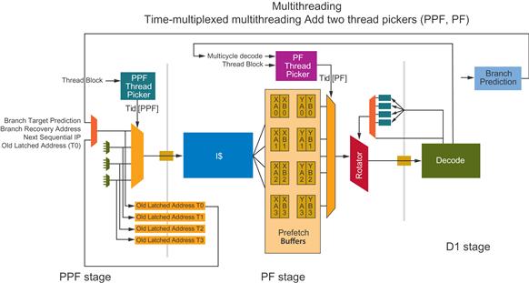
Figure 8.6 Intel® Xeon Phi™ Coprocessor Silicon Core Multithreading Architecture.
Each of four hardware threads has a “ready to run” buffer consisting of two instruction bundles. Since each core is capable of issuing two instructions per clock cycle, each bundle represents two instructions. If the executing thread has a control transfer to a target that is not contained in this buffer, it will trigger a miss to the instruction cache, which flushes the context buffer and loads the appropriate target instructions. If the instruction cache does not have the control transfer point, a core stall will be initiated, which may result in performance penalties.
In general, whichever hardware context issues instructions in a given clock cycle has priority for fetching the next instruction(s) from the instruction cache. Another significant function is the picker function (PF) that chooses the next hardware context to execute. The PF behaves in a round-robin manner, issuing instructions during any one-clock cycle from a single hardware context. In cycle N, if the PF issues instruction(s) from Context 3, then in cycle N+1 the PF will try to issue instructions from Context 0, Context 1, or Context 2—in that order. As previously noted, it is not possible to issue instructions from the same context (Context 3 in this example) in back-to-back cycles.
Scalar unit instructions execute with 1-clock latency, while most vector instructions have a 4-clock latency with 1-clock throughput. More details on specific instruction pairing guidelines, latencies, and throughput can be found in the Intel® Xeon Phi™ Coprocessor Instruction Set Architecture Reference Manual referenced at the end of this chapter.
Cache organization and memory access considerations
The L2 cache organization per core is inclusive of the L1 data and instruction caches. Each core has a private (local) 512-KB L2. The L2 caches are fully coherent and can supply data to each other on-die. The private 512-KB L2 caches in aggregate comprise a total of (512-KB×# of cores) of cache on die. Common data used by multiple cores will result in copies in each local L2 for cores using the data. If no cores were to share any data or code (this is highly unlikely), then the effective total L2 size of the chip is 30.5 MB in a 61-core coprocessor, whereas, if every core shares exactly the same code and data in perfect synchronization, then the effective total L2 size of the chip is only 512 KB. Therefore, the actual size of the application-perceived L2 storage is a function of the degree of code and data sharing among cores and threads.
The key coprocessor cache structure parameters are listed in Table 8.1.
Table 8.1
Intel® Xeon Phi™ Coprocessor Silicon Key Cache Parameters
| Parameter | L1 | L2 |
| Size | 32 KB+32 KB | 512 KB |
| Associativity | 8-way | 8-way |
| Line Size | 64 bytes | 64 bytes |
| Banks | 8 | 8 |
| Access Time | 1 cycle | 11 cycles |
| Policy | pseudo LRU | pseudo LRU |
The coprocessor silicon supports virtual memory management with 4 KB (standard), 64 KB (not standard), and 2 MB (huge and standard) page sizes available and includes Translation Lookaside Buffer (TLB) page table entry cache management to speed physical to virtual address lookup as in other Intel architecture microprocessors. On a TLB miss, the hardware performs a four-level page table walk as usual stalling the current requesting thread for many more cycles than on a hit. There is an instruction TLB (ITLB) and a two-level DTLB (L1 and L2 DTLB). The two DTLB levels have no connection with the concepts of L1 or L2 caches; it is simply a two level DTLB. The coprocessor’s TLB characteristics are shown in Table 8.2.
Table 8.2
Intel® Xeon Phi™ Coprocessor Silicon TLB Parameters

In the L2 TLB, there are no restrictions on mixing page size entries. Of course, the use of smaller page size entries will result in less overall memory mapped and available for fastest access. Four-kilobyte pages have been the long-time primary standard supported by Linux operating systems. As of this writing, 64-KB page support is not prevalent in existing microprocessors and generally will not be available without specific support additions to the Linux kernel and therefore currently goes unused. Two-megabyte huge page support is available, but the application and/or environment may need modification to specifically request it. Using huge pages for large data sets and arrays can provide a significant performance boost by reducing TLB misses versus using the default of 4-KB pages depending on the application memory access patterns. However, to ensure your application uses huge pages, it may be necessary to use means other than standard library calls (malloc) to allocate memory. In C/C++, the mmap() call provides a means to request huge pages. There is also the hugetlbfs Linux library package that can be added to the environment that enables huge page support for standard allocation calls. Future Linux kernels supported on Intel Xeon Phi coprocessors may include transparent huge page support.
Prefetching
The Intel Xeon Phi coprocessor includes memory prefetching support to maximize the availability of data to the computation units of the cores. As the name implies, prefetching is a request to the coprocessor’s cache and memory access subsystem to look ahead and begin the comparatively slow process of bringing data we expect to use in the near future into the much faster to access L1 and/or L2 caches. As an analogy, have you ever played “fetch” with very eager dogs? As soon as you lift your arm to throw, they are already running to where they anticipate the ball or stick will land to retrieve it faster. That’s prefetching!
The coprocessor provides two kinds of prefetch support, software and hardware prefetching. Software prefetching is provided in the coprocessor VPU instruction set and discussed in detail in Chapter 5. The processing impact of the prefetch requests can be reduced or eliminated because the prefetch instructions can be paired on the V-pipe in the same cycle with a vector computation instruction. Compilers typically insert L1 or L2 cache prefetch instructions by default, as needed, based on the perceived access pattern of the code, so no action is necessary on the part of the application programmer. However, compiler options exist to provide further control so the programmer can to tune the prefetch insertion beyond the compiler’s defaults. See Chapter 5 for the compiler control options. Prefetching is also available on Intel Xeon processors.
Also, an L2 cache hardware prefetcher (HWP) implementation is provided in the coprocessor silicon. Figure 8.5 shows its logical location in the core’s L2 cache control logic section. Sixteen forward or backward sequential access data streams can be detected and managed by the HWP in each core. Once the stream direction is detected then multiple and as needed prefetch requests are made to maintain the data flow.
When effectively utilized with both software and hardware capability, prefetching can significant improve performance by reducing the possibility that all threads of the coprocessor will be stalled waiting for a memory operand to be accessible in the cache.
Vector processing unit architecture
Each core of the Intel Xeon Phi coprocessor silicon has a new SIMD 512-bit wide Vector Processing Unit (VPU) with a corresponding vector instruction set. The performance that the VPU brings for applications is almost always at least as important as using the many cores (up to 244 threads) on the coprocessor. The VPU can be used to process 16 single-precision or 8 double-precision elements per clock cycle. As depicted in Figure 8.7, there are 32 vector registers plus 8 mask registers that support per SIMD lane predicated execution. Prime (hint) instructions for scatter/gather memory access are also available. There is an Extended Math Unit (EMU) that supports single precision transcendental instructions supported in hardware for exponent, logarithm, reciprocal, and reciprocal square root operations. The VPUs are IEEE 754 2008 floating-point compliant and includes SP and DP-denormalized number support, and SAE (Suppress All Errors) support for improved performance on fdiv/sqrt. Support for streaming stores helps workloads that have large output arrays that are written to or initialized before being read.

Figure 8.7 Intel® Xeon Phi™ Coprocessor Vector Processing Unit Registers Set.
The eight vector mask registers are denoted with a k prefix when used in an instruction. Each mask register is sixteen bits wide and is used by the compiler in a variety of ways, including write-masking, carry/borrow flags, comparison results, and more. For instance, mask registers can allow the compiler to perform conditional (if, else) statements in vector loops maintaining high throughput even in some data dependent circumstances. A status register, VXCSR, similar in operation to an SSE status register is provided. The registers are replicated four times in the core for each of the hardware thread contexts supported.
Data type conversion to and from 32-bit or 64-bit representation occurs automatically within the same instruction cycle before and after execution respectively.
The VPU instructions support the following native data types:
For arithmetic calculations, the VPU represents values internally using 32-bit or 64-bit two’s complement plus a sign bit (duplicate of the MSB) for signed integers, and 32-bit or 64-bit plus a sign bit tied to zero for unsigned integers. The VPU represents floating-point values internally using signed-magnitude with exponent bias of 128 or 1024 to adhere to the IEEE basic single-precision or double-precision format.
The Extended Math Unit (EMU) provides 1-cycle or 2-cycle throughput single precision transcendental functions. Specifically, the hardware will provide elementary functions: reciprocal (1/X, recip), reciprocal square root (1/√X, rsqrt), base 2 exponential (2^X, exp2), and logarithm base 2 (log2). Other transcendental functions can be derived from elementary functions: division (div) using recip and multiplication (mult), square root (sqrt) using rsqrt and mult, exponential base 10 (exp) using exp2 and mult, logarithm base B (logB) using log2 and mult, and power (pow) using log2, mult and exp2.
Vector instructions
Historically, SIMD implementations have a common set of semantic operations such as add, subtract, multiply, and so forth. Where most SIMD implementations differ lies in the specific number of operands to an operator, the nature of less common operations such as data permutations, and the treatment of individual elements contained inside a vector register.
Like Intel’s AVX instructions, the Intel Xeon Phi coprocessor silicon uses a three-operand form for its vector SIMD instruction set. For any generic instruction operator, denoted by vop, the corresponding Intel® Xeon Phi™ coprocessor instruction would commonly be:
vop:::zmm1,:zmm2,:zmm3
Where zmm1, zmm2, zmm3 are vector registers, and vop is the operation (add, subtract, and so on) to perform on them. The resulting expression1 would be:
Given that the Intel architecture is a CISC design, the Intel Xeon Phi coprocessor allows the second source operand to be a memory reference, thereby creating an implicit memory load operation in addition to the vector operation. The generic representation of using such a memory source is shown as:
vop:::zmm1,:zmm2,;[ptr]
zmm1=zmm2:::vop:::MEM[ptr]
Any memory reference in the Intel Xeon Phi coprocessor instruction set conforms to standard Intel architecture conventions, so it can be a direct pointer reference ([rax]) or an indirect ([rbp] + [rcx]), and can include an immediate offset, scale, or both2 in either direct or indirect addressing form.
While these basics are relatively straightforward and universal, the Intel Xeon Phi coprocessor introduces new operations to the vector instruction set in the form of modifiers. The mask registers can be understood as one type of modifier, where most vector operations take a mask register to use as a write-mask of the result:
vop![]() :zmm1:{k1},:zmm2,:zmm3 or:[ptr]
:zmm1:{k1},:zmm2,:zmm3 or:[ptr]
In the above expression, the specifier k1 indicates that vector mask register number one is an additional source to this operation. The mask register is specified inside curly brackets {}, which indicates that the mask register is used as a write-mask register. If the vector register has COUNT elements inside it, then the interpretation of the write-mask behavior could be considered as:
for (i=0; i<COUNT; i++)
{
if (k1[i] == 1)
zmm1[i] = zmm2[i]vopzmm3[i]
}
The key observation here is that the write-mask is a nondestructive modification to the destination register; that is, where the write-mask has the value 0 no modification of the vector register’s corresponding element occurs in that position. Where the mask has the value 1, the corresponding element of the destination vector register is replaced with the result of the operation indicated by vop.
Another modifier argument that may be specified on most SIMD vector operations is a swizzle, although the specific swizzle behavior is determined by whether the arguments are from registers or memory. The first type of swizzle is only permitted when all operands to the vector operation are registers:
vop:::zmm1:[:{k1}:],:zmm2,:zmm3:[:{swizzle}:]
Here, square brackets [:] denote that the write-mask and the swizzle are optional modifiers of the instruction. A swizzle is also denoted with curly brackets {:} (just as write-masks are denoted). Conceptually, an optional swizzle modifier causes the second source argument to be modified via a data pattern shuffle for the duration of this one instruction. It does not modify the contents of the second source register, it only makes a temporary copy and modifies the temporary copy. The temporary copy is discarded at the end of the instruction.
The swizzle modifier that the Intel Xeon Phi coprocessor supports has an alternate form when used with the implicit load form. In this form, the swizzle acts as a broadcast modifier of the value loaded from memory. This means that a subset of memory may be read and then replicated for the entire width of the vector architecture. This can be useful for vector expansion of a scalar, for repeating values, or for common mathematical operations.
One subtle aspect of the Intel Xeon Phi coprocessor design is that each vector register is treated as though it entirely contains either 32-bit or 64-bit elements. Figure 8.8 depicts the organization of the vector register when working with 32-bit data.

Figure 8.8 Per Element Vector Organization When Operating on 16 Elements of 32-bit Data.
When executing an Intel Xeon Phi coprocessor vector instruction, all arithmetic operations are carried out at either 32-bit or 64-bit granularity. This means that, when manipulating data of a different native size such as a two-byte float called float16, a different mathematical result might be obtained than if the operation were carried out with native float16 hardware. This can cause bit-differences between an expected result and the actual result, triggering violations of commutativity or associativity rules.
Intel Xeon Phi coprocessor includes IEEE 754-2008 [(Institute of Electrical and Electronics Engineers Standard for Floating Point Arithmetic, 2008)]-compliant, fused multiply-add (FMA) and fused multiply-subtract (FMS) instructions as well. These instructions produce results that are accurate to 0.5 ulp3 (one-rounding) as compared to separate multiply and add instructions back-to-back, as well as, the “fused” multiply-add instructions of other architectures that produce results of 1.0 ulp (two-rounding). In the case of Intel Xeon Phi coprocessor’s fused instructions, the basic three-operand instruction form is interpreted slightly differently:
zmm1=zmm1:::vop1:::zmm2:::vop2:::zmm3
FMA operations, for example, may have vop1 set to × and vop2 set to +. The reality is richer than this. As mentioned previously, the ability to perform implicit memory loads for the second source argument zmm3, or to apply swizzles, conversions, or broadcasts to the second source argument, allows a wider range of instruction possibilities. In the presence of FMA and FMS, however, this restriction may lead to cumbersome workarounds to place the desired source field as the second source in the instruction.
Therefore, the Intel Xeon Phi coprocessor instruction set provides a series of FMA and FMS operations, each one numbered in a sequence of three digits to the order field interpretation. This allows the use of the modifiers without knowing the particulars of the features. For example, the FMA operation for 32-bit floating-point data comes with these variants: vmadd132ps, vmadd213ps, and vmadd231ps. The logical interpretation is seen from the numeric string embedded in each mnemonic:
vfmadd132ps:::zmm1,zmm2,zmm3 : zmm1=zmm1×zmm3+zmm2
vfmadd213ps:::zmm1,zmm2,zmm3 : zmm1=zmm2×zmm1+zmm3
vfmadd231ps:::zmm1,zmm2,zmm3 : zmm1=zmm2×zmm3+zmm1
Memory loads, modifiers such as swizzle, conversion, or broadcast, are only applicable to the zmm3 term. By selecting a mnemonic, you can apply the modifiers to different locations in the functional expression.
The Intel Xeon Phi coprocessor also introduces a special fused multiply-add operation that acts as a scale and bias transformation in one instruction: vfmadd233ps. The interpretation of this instruction can be summarized in a series of equations. The vfmadd233ps of the form vfmadd233ps: ![]() ,
, ![]() ,
, ![]() generates the following:
generates the following:
The Intel Xeon Phi coprocessor also introduces vector versions of the carry-propagate instructions (CPI). As with scalar Intel architecture carry-propagate instructions, these can be combined together to support wider integer arithmetic than the hardware default. These are also building blocks for other forms of wide-arithmetic emulations. The challenge incurred in the vector version of these instructions (discussed in detail later on) is that a carry-out flag must be generated for each element in the vector. Similarly, on the propagation side, a carry-in flag must be added for each element in the vector. The Intel Xeon Phi coprocessor uses the vector mask register for both of these: as a carry-out bit vector and as a carry-in bit vector.
There are many other additions to the Intel Xeon Phi coprocessor instruction set, for use in both scalar and vector operations. A deeper, more detailed description may be found in the Intel Xeon Phi Coprocessor Instruction Set Reference Manual referenced in the “For More Information” section at the end of this chapter.
Coprocessor PCIe system interface and DMA
The Intel Xeon Phi coprocessor card complies with the Gen2 x16 PCI Express specification. PCI Express peer-to-peer writes and reads are also supported allowing direct communication with other PCI Express devices on the platform without host memory staging required. All data exchanges onto and off of the coprocessor traverses the PCI Express bus. Two primary means are provided to exchange data, memory-mapped virtual addressing, and DMA. Low latency memory-mapped address spaces on both the card and the host platform allow standard instructions on the processor or coprocessor to read or write data to the others address space. This is typically best for shorter data transfers and messages. Larger transfers generally benefit from asynchronous hardware managed transfers provided by the DMA logic.
DMA capabilities
Direct Memory Access (DMA) is a common hardware function within a computer system that is used to relieve the processor or coprocessor from the burden of copying large blocks of data. To move a block of data, the program constructs and fills a buffer, if one doesn’t already exist, and then writes a descriptor into the DMA Channel’s Descriptor Ring. A descriptor describes details such as the source and target memory addresses and the length of data in cache lines. The following data transfers are supported:
• Intel Xeon Phi coprocessor to Intel Xeon Phi coprocessor GDDR5 space (aperture)
• Intel Xeon Phi coprocessor GDDR5 to host System Memory
• Host System Memory to Intel Xeon Phi coprocessor GDDR5 (aperture or non-aperture)
• Intra-GDDR5 Block Transfers within Intel Xeon Phi coprocessor
A DMA Descriptor Ring is programmed by either the coprocessor operating system or the Host Driver. Up to eight Descriptor Rings can be opened by software; each being referred to as a DMA Channel. The coprocessor operating system or Host Driver can open a DMA Channel in either system or GDDR5 memory respectively; that is, all descriptor rings owned by the host driver must exist in system memory while rings owned by the coprocessor operating system must exist in GDDR5 memory. A programmable arbitration scheme resolves access conflicts when multiple DMA Channels vie for system or Intel Xeon Phi coprocessor resources.
The coprocessor supports host-initiated or device-initiated PCI Express Gen2/Gen1 memory, I/O, and configuration transactions. The coprocessor device-initiated memory transactions can be generated either from execution cores directly or by using the DMA engine in the SBOX.
In summary, the DMA controller has the following capabilities:
• Eight DMA channels operating simultaneously, each with its own independent hardware ring buffer that can live in either local coprocessor or system memory
• Supports transfers in either direction (host/coprocessor devices)
• Supports transfers initiated by either side
• Always transfers using physical addresses
• Interrupt generation upon completion
• 64-byte granularity for alignment and size
• Writing completion tags to either local coprocessor memory or host system
The DMA block operates at the coprocessor core clock frequency. There are eight independent channels that can move data:
The coprocessor not only supports 64-bytes (1 cache line) per PCI Express transaction, but up to a maximum of 256 bytes for each DMA-initiated transaction. This requires that the Root-Complex support 256-byte transactions. Programming the MAX_PAYLOAD_SIZE in the PCI_COMMAND_STATUS register sets the actual size of each transaction.
DMA channel arbitration
There is no notion of priority between descriptors within a DMA Channel; descriptors are fetched, and operated on, in a sequential order. Priority between descriptors is resolved by opening multiple DMA channels and performing arbitration between DMA channels in a round-robin fashion.
Descriptor ring overview
A Descriptor Ring is a circular buffer as shown in Figure 8.9. The length of a Descriptor Ring can be up to 128-KB entries, and must align to the nearest cache line boundary. Software manages the ring by advancing a Head Pointer as it fills the ring with descriptors. When the descriptors have been copied, it writes this updated Header Pointer into the DMA Head Pointer Register (DHPR0–DHPR7) for the appropriate DMA Channel. Each DMA Channel contains a Tail Pointer that advances as descriptors are fetched into a channel’s Local Descriptor Queue. The Descriptor Queue is 64 entries, and can be thought of as a sliding window over the Descriptor Ring. The Tail Pointer is periodically written back to memory so that software can track its progress. Upon initialization, software sets both the Head Pointer and Tail Pointer to point to the base of the Descriptor Ring. From the DMA Channel perspective, an empty state is approached when the Tail Pointer approaches the Head Pointer. From a software perspective, a full condition is approached when the Head Pointer approaches the Tail Pointer.

Figure 8.9 DMA Channel Descriptor Ring Plus Local Descriptor Queue.
The Head and Tail Pointers are addresses. If the high-order bit is a 1, the descriptors reside in system memory; otherwise they reside in the Intel Xeon Phi coprocessor memory. Descriptors come in five different formats and are 16 bytes in length. There are no alignment restrictions when writing descriptors into the ring. However, performance is optimized when descriptors start and end on cache line boundaries because memory accesses are performed on cache line granularities, four descriptors at a time.
Coprocessor power management capabilities
Intel Xeon Phi coprocessor power management supports several Intel architecture standard power management states. Unlike the multicore family of Intel Xeon processors, there is no hardware-level power control unit (PCU); power management is controlled by the coprocessor operating system described in Chapter 10. The Intel Xeon Phi System Software Developers Guide referenced in the “For More Information” section at the end of this chapter has a detailed description of the power management features.
Figures 8.10 through 8.15 provide a visual description of the power management states supported on the coprocessor.

Figure 8.10 C0: All Coprocessor Silicon Cores and Components Running.

Figure 8.11 Single Core C1 State: Clock Gate Core.

Figure 8.12 Single Core C6 State: Power Gate Core.
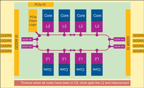
Figure 8.13 Whole Package Auto C3: Clock Gate L2 Cache and On-Die Interconnect.

Figure 8.14 Whole Package Deep C3.
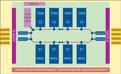
Figure 8.15 Whole Package C6: Lowest Power State.
Reliability, availability, and serviceability (RAS)
RAS stands for reliability, availability, and serviceability. Specifically, reliability is defined as the ability of the system to perform its actions correctly. Availability is the ability of the system to perform useful work. Serviceability is the ability of the system to be repaired when failures occur. Given that high performance long-running computing tasks may require large amounts of resources both in processing power (count of processing entities or nodes) and in processing time, node reliability becomes a limiting factor if not addressed by RAS strategies and policies. This section covers RAS strategies available in hardware and software on Intel Xeon Phi coprocessor and its host-side server.
In compute clusters, reliability and availability are traditionally handled in a two-pronged approach: by deploying hardware with advanced RAS features to reduce error rates (as exemplified in the Intel Xeon processors) and by adopting fault tolerance in high-end system software or hardware. Common software-based methods of fault tolerance are to deploy redundant cluster nodes or to implement snapshot and restore (checkpointing) mechanisms that allow a cluster manager to reduce data loss when a compute node fails by setting it to the state of last successful snapshot. Fault tolerance, in this context, is about resuming from a failure with as much of the machine state intact as possible. It does not imply that a cluster or individual compute nodes can absorb or handle failures without interrupting the task at hand.
The Intel Xeon Phi coprocessor addresses reliability and availability the same two ways. Hardware features have been added that improve reliability; for example, standard Error Correcting Codes (ECC) on both GDDR5 memory and internal memory arrays that reduce error rates. There are also additional parity checks built into critical circuits. Fault tolerance on Intel Xeon Phi coprocessor hardware improves failure detection (extended machine check architecture, or MCA). Managed properly, the result is a controlled and limited degradation allowing a node to stay in service after certain anticipated hardware failure modes manifest themselves. Fault tolerance in Intel Xeon Phi coprocessor software is assisted by the Linux coprocessor operating system, which supports application-level snapshot and restore features that are based on BLCR (Berkeley Labs Checkpoint Restart).
The Intel Xeon Phi coprocessor approach to serviceability is through software redundancy (that is, node management removes failing compute nodes from the cluster), and has no true hardware redundancy. Instead software and firmware features allow a compute node to reenter operation after failures at reduced capacity until the card can be replaced. The rationale behind this “graceful” degradation strategy is the assumption that an Intel Xeon Phi coprocessor unit with, say, one less core, will be able to resume application snapshots and therefore is a better proposition to the cluster than removing the node entirely.
A hardware failure requires the failing card to be temporarily removed from the compute cluster it is participating in. After a reboot, the card may rejoin the cluster if cluster management policies allow for it. The rebooted card may have the previously mentioned “graceful” degradation if persistent errors require turning off nonfunctional cores or parts of L2 cache, and so on.
Machine check architecture (MCA)
Machine Check Architecture is a hardware feature enabling an Intel Xeon Phi coprocessor card to report failures to software by means of interrupts or exceptions. Failures in this context are conditions where logic circuits have detected something out of order, which may have corrupted processor context or memory content. Failures are categorized by severity as either DUEs or CEs:
• DUEs (Detected Unrecoverable Errors) are errors captured by the MC logic but the corruption cannot be repaired and the system as a whole is compromised; for example, errors in L1 cache.
• CEs (Corrected Errors) are errors that have occurred and been corrected by the hardware, such as single bit errors in L2 ECC memory.
Standard Intel architecture systems implement MCA by providing two mechanisms to report MC events to software: MC exceptions (#18) for events detected in the core and NMI (#2) interrupts for events detected outside of the core (uncore).
Specifics on occurred MC exceptions are presented in MSR banks, each representing up to 32 events. The processor capability MSRs specify how many banks are supported by a given processor. The interpretation of data in MSR banks is semi-standardized; acquiring detailed raw data on an event is standardized but the interpretation of acquired raw data is not. The Intel Xeon Phi coprocessor provides three MC MSR banks.
MC events signaled through the NMI interrupt on standard Intel architecture systems come from the chipsets and represent failures in memory or I/O paths. Newer processors with built-in memory controllers also provide a separate interrupt for CEs (CMCIs) that have built-in counter dividers to throttle interrupt rates. This capability is not provided on the Intel Xeon Phi coprocessor. Instead, the coprocessor delivers both uncorrected and corrected errors that are detected in the core domain via the standard MCA interrupt (#18). Machine check events that occur in the uncore domain are delivered via the System Interface, which can be programmed to generate an NMI interrupt targeted at one or all threads. The Uncore Interrupt includes MC events related to the PCI-Express interface, Memory Controller (ECC and link training errors), or other uncore units. There is no CE error rate throttle in the coprocessor. If high error frequencies interfere with operations unnecessarily it is possible to disable the interrupt at the source of the initiating unit (L2/L1 Cache, Tag Directory, or Memory Controller).
The NMI interrupt handler software must handle a diverse range of error types on Intel Xeon Phi coprocessor. Registers to control and report uncore MC events on the coprocessor differ significantly from registers on standard Intel architecture chipsets, which means that stock operating systems have no support for uncore MC events on a coprocessor.
The Intel Xeon Phi coprocessor implements extended machine check architecture (MCA) features that allow software to detect and act on detected hardware failures in a manner allowing a “graceful” degradation of service when certain components fail. Coprocessor hardware reads bits from programmable flash memory at boot time, which may disable processor cores, cache lines, and tag directories that the MCA has reported as failing. More details on the key RAS architecture elements is available in the Intel Xeon Phi System Software Developers Guide referenced in the “For More Information” section at the end of this chapter.
Coprocessor system management controller (SMC)
As essentially a full computing platform packaged in a PCI Express card, features for users, administrators, and baseboard management controller software (BMC) are provided to monitor and manage the Intel Xeon Phi coprocessor. One key component enabling that manageability is an intelligent, firmware driven System Management Controller (SMC) on the card as shown in Figure 8.2.
The SMC is a microcontroller-based thermal management and communications sub-system that provides card-level control and monitoring of the coprocessor. Thermal management is achieved through monitoring the coprocessor silicon and various temperature sensors located on the coprocessor card. Card-level power management monitors the card input power draw and communicates current power conditions to the coprocessor silicon and its operating software.
The SMC communicates information via two communication channels. Communication with the onboard coprocessor silicon is done via a standard I2C interface. Out of band communication with the host platform is done via the PCI Express supported System Management Bus (SMBus) using the industry standard Intelligent Platform Management Interface (IPMI) protocol.
Sensors
Thermal sensors located on the Intel Xeon Phi coprocessor provide information about the coprocessor silicon temperature as well as the temperature from three locations on the Intel Xeon Phi coprocessor card. Currently, one sensor is located between memory chips near the PCI Express slot while the other two are located on the east and west sides of the card. These east and west sensors are generally referred to as the “inlet” and “outlet” air temperature sensors but they do not actually indicate airflow temperatures but rather the temperature of each side of the card. These sensors can be correlated to air temperature for purposes of system thermal management.
Power sensors are attached to the power inputs from the PCI Express slot, and the two (2×3 and 2×4) auxiliary power connectors on the coprocessor card. Input power can be estimated by summing the currents over these three power connections.
Thermal design power monitoring and control
To support maintaining the coprocessor’s target Thermal Design Power (TDP) level, there as several mechanisms in the SMC to signal the host and/or coprocessor silicon when thermal or power consumption limits are reached. Two programmable power consumption limits are provided and managed by the SMC. One limit defaults to 105 percent of the TDP power consumption. If this first level limit is exceeded, the SMC notifies the Intel Xeon Phi coprocessor operating system through an interrupt to reduce power by lowering the coprocessor silicon’s clock speed by 100 MHz. The second power limit occurs at 125 percent generating a “throttling event,” which drops to the lowest supported clock speed on the coprocessor silicon, (600–800 MHz depending on the model) in an attempt to reduce power at or below the TDP. When the SMC detects and communicates a reduction below the primary limit the core clock is restored to its nominal rate.
The SMC also monitors the thermal sensors for a maximum card temperature threshold limit. If that limit is reached then a thermal throttling condition occurs causing the coprocessor silicon to drop to its lowest supported clock speed. Again, when the temperature state is restored to operational levels the clock returns to its nominal speed.
Alternatively, on Intel Xeon Phi coprocessor models with passive thermal solutions, the host platform’s baseboard management solution can utilize the PCI Express card’s B12 pin to assert a coprocessor card signal known as PROCHOT that is monitored by the SMC. This allows platform level thermal monitoring to request the card perform thermal throttling in support of overall platform thermal reduction.
Fan speed control
For an actively cooled card, the SMC will automatically increase and decrease the fan speed to maintain card temperature within specified limits. If the card exceeds the maximum thermal threshold the actively cooled fan will be placed at maximum speed in addition to the throttling mechanism dropping the coprocessor silicon clock to its minimum supported speed.
Potential application impact
The key impact for applications of thermal and power events is unexpected performance loss or lack of consistent, repeatable performance over multiple test runs since the primary mitigation for thermal and power issues is to lower the coprocessor clock below its nominal rate. In normal circumstances, the majority of applications should not be the cause of thermal or power events. However, should you experience unexplainable performance degradation or variability on repeated runs on the same node or across identical nodes then checking for power or thermal events by contacting your system administrator or using the available coprocessor monitoring tools described further in Chapter 9 would be something to consider.
Benchmarks
Since Intel Xeon Phi coprocessors come in so many models, and new versions are likely to continue to emerge, we choose to not dedicate pages of this book to benchmarking. Intel and some users have published a number of benchmarks already, and we will see more in the future. The Internet is an excellent resource for finding the latest claims and publications.
It is useful to note that Intel took a decidedly refreshing approach to benchmarking, which at first glance makes their benchmark numbers seem small. Intel choose to only compare the Intel Xeon Phi coprocessors when running optimized workloads to a pair of recent Intel Xeon processors also running optimized workloads. That breaks with a common practice in accelerator benchmarking of comparing an unoptimized (often single-threaded) workloads running on a (often older) processor against a highly optimized accelerator workload. In such situations, gains of “100X” could be claimed regardless of the relevance of such a comparison. Intel’s approach results in some claims “only” in the “2X” realm, but along with claims of beating accelerators in terms of performance and power efficiency despite the seeming contradiction of “100X” claims by the accelerators.
Intel’s choice to compare against two processors, instead of one, is an interesting one to understand as well. It turns out that two processors are closer in power consumption to a single coprocessor (or accelerator) than one processor is. This choice to level the playing field based on power consumption makes sense technically, it will remain to be seen if the market appreciates the approach. Given the intense interest in power efficiency, it seems likely Intel is onto something important here.
Summary
The Intel Xeon Phi coprocessor is optimized for highly parallel workloads while retaining the support for familiar programming languages, models and tools you would expect from a symmetric multiprocessing (SMP) system built around Intel processors. This chapter helps explain in detail the particulars of this SMP design, including the wider vector units that contribute an important parallel capability in addition to the large number of processing cores. The use of simpler core designs allow for more cores to fit on a single die, but important very modern features including power management are in the coprocessor also. The Intel Xeon Phi coprocessor takes advantage of having all the cores and their caches on a single die to offer performance characteristics that a discrete SMP system could not. Future products that use the Intel MIC architecture may differ from this first Intel Xeon Phi coprocessor design, but the vision for the architecture of highly parallel, highly power efficient and highly programmable shines through in this very first product to use the Intel MIC architecture from Intel.
For more information
Here are some additional reading materials we recommend related to this chapter:
• Intel® MIC Quick Start Developers Guide, http://intel.com/software/mic
• Datasheet for the Intel® Xeon Phi™ Coprocessor, http://tinyurl.com/xeonphidatasheet
• Intel® Many Integrated Core Platform Software Stack, http://intel.com/software/mic
• Intel® Xeon Phi™ Coprocessor Instruction Set Architecture Reference Manual, http://intel.com/software/mic
• An Overview of Programming for Intel® Xeon® processors and Intel® Xeon Phi™ coprocessors, http://intel.com/software/mic
• Debugging Intel® Xeon Phi™ Coprocessor: Command-Line Debugging, http://intel.com/software/mic
• Building Native Applications for Intel® Xeon Phi™ Coprocessor, http://intel.com/software/mic
• Programming and Compiling for Intel® Many Integrated Core Architecture, http://intel.com/software/mic
• Intel® Xeon Phi™ coprocessor Micro-architecture Software Stack, http://intel.com/software/mic
• Intel® Xeon Phi™ coprocessor Micro-architecture Overview, http://intel.com/software/mic
• Intel® MPI Library, http://www.intel.com/go/mpi
• Intel® MIC SCIF API Reference Manual for Kernel Mode Linux, http://intel.com/software/mic
• Intel® MIC SCIF API Reference Manual for User Mode Linux, http://intel.com/software/mic
• Intelligent Platform Management Interface Specifications, http://tinyurl.com/intelipmi
• Hotchips presentation about Intel Xeon Phi coprocessor by the lead architect for the Intel Xeon Phi coprocessor. Transcript at http://tinyurl.com/georgehotchips and presentation at http://tinyurl.com/georgehotchipspdf.
1This is true for two-operand operators, such as arithmetic+or ×. For those operators that require additional operands, such as carry-propagate instructions or fused multiply-add, a different form is used.
2For instance, an address could be of the form [rbp]+([rax]*2)+0xA43C0000.
3Unit in the Last Place (ulp), a measure of the accuracy of the least significant bit in a result.