
Chapter 3
AD/DA Conversions
The conversion of a continuous-time function x(t) (voltage, current) into a sequence of numbers x(n) is called analog-to-digital conversion (AD conversion). The reverse process is known as digital-to-analog conversion (DA conversion). The time-sampling of a function x(t) is described by Shannon's sampling theorem. This states that a continuous-time signal with bandwidth fB can be sampled with a sampling rate fS > 2fB without changing the information content in the signal. The original analog signal is reconstructed by low-pass filtering with bandwidth fB. Besides time-sampling, the nonlinear procedure of digitizing the continuous-valued amplitude (quantization) of the sampled signal occurs. In Section 3.1 basic concepts of Nyquist sampling, oversampling and delta-sigma modulation are presented. In Sections 3.2 and 3.3 principles of AD and DA converter circuits are discussed.
3.1 Methods
3.1.1 Nyquist Sampling
The sampling of a signal with sampling rate fS > 2fB is called Nyquist sampling. The schematic diagram in Fig. 3.1 shows the procedure. The band-limiting of the input at fS/2 is carried out by an analog low-pass filter (Fig. 3.1a). The following sample-and-hold circuit samples the band-limited input at a sampling rate fS. The constant amplitude of the time function over the sampling period TS = 1/fS is converted to a number sequence x(n) by a quantizer (Fig. 3.1b). This number sequence is fed to a digital signal processor (DSP) which performs signal processing algorithms. The output sequence y(n) is delivered to a DA converter which gives a staircase as its output (Fig. 3.1c). Following this, a low-pass filter gives the analog output y(t) (Fig. 3.1d). Figure 3.2 demonstrates each step of AD/DA conversion in the frequency domain. The individual spectra in Fig. 3.2a–d correspond to the outputs in Fig. 3.1a–d.
After band-limiting (Fig. 3.2a) and sampling, a periodic spectrum with period fS of the sampled signal is obtained as shown in Fig. 3.2b. Assuming that consecutive quantization errors e(n) are statistically independent of each other, the noise power has a spectral uniform distribution in the frequency domain 0 ≤ f ≤ fS. The output of the DA converter still has a periodic spectrum. However, this is weighted with the sinc function (sinc = sin(x)/x), of the sample-and-hold circuit (Fig. 3.2c). The zeros of the sinc function are at multiples of the sampling rate fS. In order to reconstruct the output (Fig. 3.2d), the image spectra are eliminated by an analog low-pass of sufficient stop-band attenuation (see Fig. 3.2c).
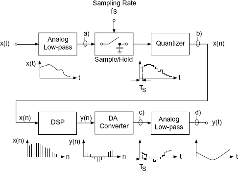
Figure 3.1 Schematic diagram of Nyquist sampling.

Figure 3.2 Nyquist sampling – interpretation in the frequency domain.
The problems of Nyquist sampling lie in the steep band-limiting filter characteristics (anti-aliasing filter) of the analog input filter and the analog reconstruction filter (anti-imaging filter) of similar filter characteristics and sufficient stop-band attenuation. Further, sinc distortion due to the sample-and-hold circuit needs to be compensated for.
3.1.2 Oversampling
In order to increase the resolution of the conversion process and reduce the complexity of analog filters, oversampling techniques are employed. Owing to the spectral uniform distribution of quantization error between 0 and fS (see Fig. 3.3a), it is possible to reduce the power spectral density in the pass-band 0 ≤ f ≤ fB through oversampling by a factor L, i.e. with the new sampling rate LfS (see Fig. 3.3b). For identical quantization step size Q, the shaded areas (quantization error power ![]() ) in Fig. 3.3a and Fig. 3.3b are equal. The increase in the signal-to-noise ratio can also be observed in Fig. 3.3.
) in Fig. 3.3a and Fig. 3.3b are equal. The increase in the signal-to-noise ratio can also be observed in Fig. 3.3.

Figure 3.3 Influence of oversampling and delta-sigma technique on power spectral density of quantization error and on input sinusoid with frequency f1.
It follows that in the pass-band at a sampling rate of fS = 2fB the power spectral density given by
Owing to oversampling by a factor of L, a reduction of the power spectral density given by
is obtained (see Fig. 3.3b). With fS = 2fB, the error power in the audio band is given by
The signal-to-noise ratio (with ![]() ) owing to oversampling can now be expressed as
) owing to oversampling can now be expressed as
Figure 3.4a shows a schematic diagram of anoversampling AD converter. Owing to oversampling, the analog band-limiting low-pass filter can have a wider transition bandwidth as shown in Fig. 3.4b. The quantization error power is distributed between 0 and the sampling rate LfS. To reduce the sampling rate, it is necessary to limit the bandwidth with a digital low-pass filter (see Fig. 3.4c). After this, the samplingrate is reduced by a factor L (see Fig. 3.4d) by taking every Lth output sample of the digital low-pass filter [Cro83, Vai93, Fli00].
Figure 3.5a shows a schematic diagram of an oversampling DA converter. The sampling rate is first increased by a factor of L. For this purpose, L − 1 zeros are introduced between two consecutive input values [Cro83, Vai93, Fli00]. The following digital filter eliminates all image spectra (Fig. 3.5b) except the base-band spectrum and spectra at multiples of LfS (Fig. 3.5c). It interpolates L − 1 samples between two input samples. The w-bit DA converter operates at a sampling rate LfS. Its output is fed to an analog reconstruction filter which eliminates the image spectra at multiples of LfS.
3.1.3 Delta-sigma Modulation
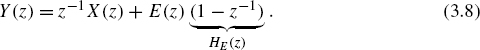
Delta-sigma modulation using oversampling is a conversion strategy derived from delta modulation. In delta modulation (Fig. 3.6a), the difference between the input x(t) and signal x1(t) is converted into a 1-bit signal y(n) at a very high sampling rate LfS. The sampling rate is higher than the necessary Nyquist rate fS. The quantized signal y(n) gives the signal x1(t) via an analog integrator. The demodulator consists of an integrator and a reconstruction low-pass filter.
The extension to delta-sigma modulation [Ino63] involves shifting the integrator from the demodulator to the input of the modulator (see Fig. 3.6b). With this, it is possible to combine the two integrators as a single integrator after addition (see Fig. 3.7a). The corresponding signals are shown in Fig. 3.8.

Figure 3.4 Oversampling AD converter and sampling rate reduction.
A time-discrete model of the delta-sigma modulator is given in Fig. 3.7b. The Z- transform of the output signal y(n) is given by
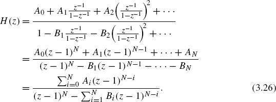
For a large gain factor of the system H(z), the input signal will not be affected. In contrast, the quantization error is shaped by the filter term 1/[(1 + H(z)].
Schematic diagrams of delta-sigma AD/DA conversion are shown in Figs 3.9 and 3.10. For delta-sigma AD converters, a digital low-pass filter and a downsampler with factor L are used to reduce the sampling rate LfS to fS. The 1-bit input to the digital low-pass filter leads to a w-bit output x(n) at a sampling rate fS. The delta-sigma DA converter consists of an upsampler with factor L, a digital low-pass filter to eliminate the mirror spectra and a delta-sigma modulator followed by an analog reconstruction low-pass filter. In order to illustrate noise shaping in delta-sigma modulation in detail, first- and second-order systems as well as multistage techniques are investigated in the following sections.

Figure 3.5 Oversampling and DA conversion.
First-order Delta-sigma Modulator
A time-discrete model of a first-order delta-sigma modulator is shown in Fig. 3.11.
The difference equation for the output y(n) is given by
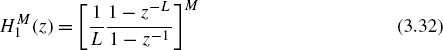
The corresponding Z-transform leads to
The power density spectrum of the error signal e1(n) = e(n) − e(n − 1) is
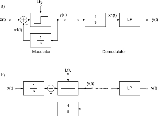
Figure 3.6 Delta modulation and displacement of integrator.

Figure 3.7 Delta-sigma modulation and time-discrete model.
where SEE(ejΩ) denotes the power density spectrum of the quantization error e(n). The error power in the frequency band [−fB, fB], with SEE(f) = Q2/12LfS, can be written as


Figure 3.8 Signals in delta-sigma modulation.

Figure 3.9 Oversampling delta-sigma AD converter.
With fS = 2fB, we get
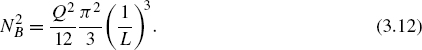

Figure 3.10 Oversampling delta-sigma DA converter.

Figure 3.11 Time-discrete model of a first-order delta-sigma modulator.
Second-order Delta-sigma Modulator
For the second-order delta-sigma modulator [Can85], shown in Fig. 3.12, the difference equation is expressed as
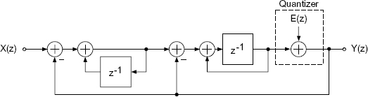
Figure 3.12 Time-discrete model of a second-order delta-sigma modulator.
and the Z-transform is given by
The power density spectrum of the error signal e1(n) = e(n) − 2e(n − 1) + e(n − 2) can be written as

The error power in the frequency band [−fB, fB] is given by
and with fS = 2fB we obtain

Multistage Delta-sigma Modulator
A multistage delta-sigma modulator (MASH, [Mat87]) is shown in Fig. 3.13.

Figure 3.13 Time-discrete model of a multistage delta-sigma modulator.
The Z-transforms of the output signals yi(n), i = 1, 2, 3, are given by
The Z-transform of the output obtained by addition and filtering leads to

The error power in the frequency band [−fB, fB],

with fS = 2fB, gives the total noise power

The error transfer functions in Fig. 3.14 show the noise shaping for three types of delta-sigma modulations as discussed before. The error power is shifted toward higher frequencies.

Figure 3.14 HE(z) = (1 − z−1)K with K = 1, 2, 3.
The improvement of signal-to-noise ratio by pure oversampling and delta-sigma modulation (first, second and third order) is shown in Fig. 3.15. For the general case of a kth-order delta-sigma conversion with oversampling factor L one can derive the signal-to-noise ratio as
Here w denotes the quantizer word-length of the delta-sigma modulator. The signal quantization after digital low-pass filtering and downsampling by L can be performed with (3.25) according to the relation w = SNR/6.

Figure 3.15 Improvement of signal-to-noise ratio as a function of oversampling and noise shaping (L = 2x).
Higher-order Delta-sigma Modulator
A widening of the stop-band for the high-pass transfer function of the quantization error is achieved with higher-order delta-sigma modulation [Cha90]. Besides the zeros at z = 1, additional zeros are placed on the unit circle. Also, poles are integrated into the transfer function. A time-discrete model of a higher-order delta-sigma modulator is shown in Fig. 3.16.

Figure 3.16 Higher-order delta-sigma modulator.
The transfer function in Fig. 3.16 can be written as
The Z-transform of the output is given by
The transfer function for the input is

and the transfer function for the error signal is given by

For Butterworth or Chebyshev filter designs, the frequency responses as shown in Fig. 3.17 are obtained for the error transfer functions. As a comparison, the frequency responses of first-, second- and third-order delta-sigma modulation are shown. The widening of the stop-band for Butterworth and Chebyshev filters can be observed from Fig. 3.18.
Decimation Filter
Decimation filters for AD conversion and interpolation filters for DA conversion are implemented with multirate systems [Fli00]. The necessary downsampler and upsampler are simple systems. For the former, every nth sample is taken out of the input sequence. For the latter, n − 1 zeros are inserted between two input samples. For decimation, band-limiting is performed by H(z) followed by sampling rate reduction by a factor L. This procedure can be implemented in stages (see Fig. 3.19). The use of easy-to-implement filter structures at high sampling rates, like comb filters with transfer function
(shown in Fig. 3.20), allows simple implementation needing only delay systems and additions. In order to increase the stop-band attenuation, a series of comb filters is used so
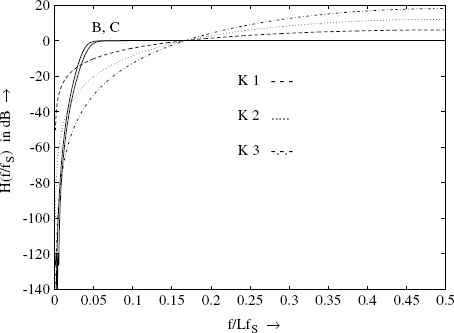
Figure 3.17 Comparison of different transfer functions of error signal.

Figure 3.18 Transfer function of the error signal in stop-band.
that
is obtained.
Besides additions at high sampling rates, complexity can be reduced further. Owing to sampling rate reduction by a factor of L, the numerator (1 − z−L) can be moved so that it is placed after the downsampler (see Fig. 3.21). For a series of comb filters, the structure in Fig. 3.22 results. M simple recursive accumulators have to be performed at the high sampling rate LfS. After this, downsampling by a factor L is carried out. The M nonrecursive systems are calculated with the output sampling rate fS.

Figure 3.19 Several stages of sampling rate reduction.

Figure 3.20 Signal flow diagram of a comb filter.

Figure 3.21 Comb filter for sampling rate reduction.

Figure 3.22 Series of comb filters for sampling rate reduction.
Figure 3.23a shows the frequency responses of a series of comb filters (L = 16). Figure 3.23b shows the resulting frequency response for the quantization error of a third-order delta-sigma modulator connected in series with a comb filter ![]() . The system delay owing to filtering and sampling rate reduction is given by
. The system delay owing to filtering and sampling rate reduction is given by
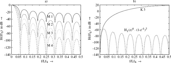
Figure 3.23 (a) Transfer function ![]() with M = 1…4. (b) Third-order delta-sigma modulation and in series with
with M = 1…4. (b) Third-order delta-sigma modulation and in series with ![]() .
.
Example: Delay time of conversion process (latency time)
- Nyquist conversion

- Delta-sigma modulation with single-stage downsampling
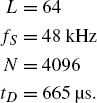
- Delta-sigma modulation with two-stage downsampling

3.2 AD Converters
The choice of an AD converter for a certain application is influenced by a number of factors. It mainly depends on the necessary resolution for a given conversion time. Both of these depend upon each other and are decisively influenced by the architecture of the AD converter. For this reason, the specifications of an AD converter are first discussed. This is followed by circuit principles which influence the mutual dependence of resolution and conversion time.
3.2.1 Specifications
In the following, the most important specifications for AD conversion are presented.
Resolution. The resolution for a given word-length w of an AD converter determines the smallest amplitude
which is equal to the quantization step Q.
Conversion Time. The minimum sampling period TS = 1/fS between two samples is called the conversion time.
Sample-and-hold Circuit. Before quantization, the time-continuous function is sampled with the help of a sample-and-hold circuit, as shown in Fig. 3.24a.
The sampling period TS is divided into the sampling time tS in which the output voltage U2 follows the input voltage U1, and the hold time tH. During the hold time the output voltage U2 is constant and is converted into a binary word by quantization.

Figure 3.24 (a) Sample-and-hold circuit. (b) Input and output with clock signal. (tS = sampling time, tH = hold time, tAD = aperture delay.)
Aperture Delay. The time tAD elapsed between start of hold and actual hold mode (see Fig. 3.24b) is called the aperture delay.
Aperture Jitter. The variation in aperture delay from sample to sample is called the aperture jitter tADJ. The influence of aperture jitter limits the useful bandwidth of the sampled signal. This is because at high frequency a deterioration of the signal-to-noise ratio occurs. Assuming a Gaussian PDF aperture jitter, the signal-to-noise ratio owing to aperture jitter as a function of frequency f can be written as
Offset Error and Gain Error. The offset and gain errors of an AD converter are shown in Fig. 3.25. The offset error results in a horizontal displacement of the real curve compared with the dashed ideal curve of an AD converter. The gain error is expressed as the deviation from the ideal gradient of the curve.

Figure 3.25 Offset error and gain error.
Differential Nonlinearity. The differential nonlinearity
describes the error of the step size of a certain code word in LSB units. For ideal quantization, the increase Δx in the input voltage up to the next output code xQ is equal to the quantization step Q (see Fig. 3.26). The difference of two consecutive output codes is denoted by ΔxQ. When the output code changes from 010 to 011, the step size is 1.5 LSB and therefore the differential nonlinearity DNL = 0.5 LSB. The step size between the codes 011 and 101 is 0 LSB and the code 200 is missing. The differential nonlinearity is DNL = −1 LSB.
Integral Nonlinearity. The integral nonlinearity (INL) describes the error between the quantized and the ideal continuous value. This error is given in LSB units. It arises owing to the accumulated error of the step size. This (see Fig. 3.27) changes itself continuously from one output code to another.
Monotonicity. The progressive increase in quantizer output code for a continuously increasing input voltage and progressive decrease in quantizer output code for a continuously decreasing input voltage is called monotonicity. An example of non-monotonic behavior is shown in Fig. 3.28 where one output code does not occur.

Figure 3.26 Differential nonlinearity.

Figure 3.27 Integral nonlinearity.

Total Harmonic Distortion. The harmonic distortion is calculated for an AD converter at full range with a sinusoid (X1 = 0 dB) of given frequency. The selective measurement of harmonics of the second to the ninth order are used to compute

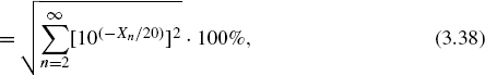
where Xn are the harmonics in dB.
THD+N: Total Harmonic Distortion plus Noise. For the calculation of harmonic distortion plus noise, the test signal is suppressed by a stop-band filter. The measurement of harmonic distortion plus noise is performed by measuring the remaining broad-band noise signal which consists of integral and differential nonlinearity, missing codes, aperture jitter, analog noise and quantization error.
3.2.2 Parallel Converter
Parallel Converter. A direct method for AD conversion is called parallel conversion (flash converter). In parallel converters, the output voltage of the sample-and-hold circuit is compared with a reference voltage UR with the help of 2w − 1 comparators (see Fig. 3.29). The sample-and-hold circuit is controlled with sampling rate fS so that, during the hold time tH, a constant voltage at the output of the sample-and-hold circuit is available. The outputs of the comparators are fed at sampling clock rate into a (2w − 1)-bit register and converted by a coding logic to a w-bit data word. This is fed at sampling clock rate to an output register. The sampling rates that can be achieved lie between 1 and 500 MHz for a resolution of up to 10 bits. Owing to the large number of comparators, the technique is not feasible for high precision.

Figure 3.29 Parallel converter.
Half-flash Converter. In half-flash AD converters (Fig. 3.30), two m-bit parallel converters are used in order to convert two different ranges. The first m-bit AD converter gives a digital output word which is converted into an analog voltage using an m-bit DA converter. This voltage is now subtracted from the output voltage of the sample-and-hold circuit. The difference voltage is digitized with a second m-bit AD converter. The rough and fine quantization leads to a w-bit data word with a subsequent logic.
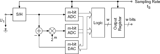
Figure 3.30 Half-flash AD converter.
Subranging Converter. A combination of direct conversion and sequential procedure is carried out for subranging AD converters (see Fig. 3.31). In contrast to the half-flash converter, only one parallel converter is required. The switches S1 and S2 take the values of 0 and 1. First the output voltage of a sample-and-hold circuit and then the difference voltage amplified by a factor 2m is fed to an m-bit AD converter. The difference voltage is formed with the help of the output voltage of an m-bit DA converter and the output voltage of the sample-and-hold circuit. The conversion rates lie between 100 kHz and 40 MHz where a resolution of up to 16 bits is achieved.

Figure 3.31 Subranging AD converter.
3.2.3 Successive Approximation
AD converters with successive approximation consist of the functional modules shown in Fig. 3.32. The analog voltage is converted into a w-bit word within w cycles. The converter consists of a comparator, a w-bit DA converter and logic for controlling the successive approximation.

Figure 3.32 AD converter with successive approximation.
The conversion process is explained with the help of Fig. 3.33. First, it is checked whether a positive or negative voltage is present at the comparator. If it is positive, the output +0.5UR is fed to a DA converter to check whether the output voltage of the comparator is greater or less than +0.5UR. Then, the output of (+0.5±0.25)UR is fed to the DA comparator. The output of the comparator is then evaluated. This procedure is performed w times and leads to a w-bit word.

Figure 3.33 Successive approximation.
For a resolution of 12 bits, sampling rates of up to 1 MHz can be achieved. Higher resolutions of more than 16 bits are possible at a lower sampling rates.
3.2.4 Counter Methods
In contrast to the conversion techniques of the previous sections for high conversion rates, the following techniques are used for sampling rates smaller than 50 kHz.
Forward-backward Counter. A technique which operates like successive approximation is the forward-backward counter shown in Fig. 3.34. A logic controls a clocked forward-backward counter whose output data word provides an analog output voltage via a w-bit DA converter. The difference signal between this voltage and the output voltage of the sample-and-hold circuit determines the direction of counting. The counter stops when the corresponding output voltage of the DA converter is equal to the output voltage of the sample-and-hold circuit.
Single-slope Counter. The single-slope AD converter shown in Fig. 3.35 compares the output voltage of the sample-and-hold circuit with a voltage of a sawtooth generator. The sawtooth generator is started every sampling period. As long as the input voltage is greater than the sawtooth voltage, the clock impulses are counted. The counter value corresponds to the digital value of the input voltage.
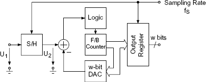
Figure 3.34 AD converter with forward-backward counter.

Figure 3.35 Single-slope AD converter.
Dual-slope Converter. A dual-slope AD converter is shown in Fig. 3.36. In the first phase in which a switch S1 is closed for a counter period t1, the output voltage of the sample-and-hold circuit is fed to an integrator of time-constant τ. During the second phase, the switch S2 is closed and the switch S1 is opened. The reference voltage is switched to the integrator and the time to reach a threshold is determined by counting the clock impulses by a counter. Figure 3.36 demonstrates this for three different voltages U2. The slope during time t1 is proportional to the output voltage U2 of the sample-and-hold circuit, whereas the slope is constant when the reference voltage UR is connected to the integrator. The ratio U2/UR = t2/t1 leads to the digital output word.
3.2.5 Delta-sigma AD Converter
The delta-sigma AD converter in Fig. 3.37 requires no sample-and-hold circuit owing to its high conversion rate. The analog band-limiting low-pass filter and the digital low-pass filter for downsampling to a sampling rate fS are usually on the same circuit. The linear phase nonrecursive digital low-pass filter in Fig. 3.37 has a 1-bit input signal and leads to a w-bit output signal owing to the N filter coefficients h0, h1,…, hN−1 which are implemented with a word-length of w bits. The output signal of the filter results from the summation of the filter coefficients (0 or 1) of the nonrecursive low-pass filter. The downsampling by a factor L is performed by taking every Lth sample out of the filter and writing to the output register. In order to reduce the number of operations the filtering and downsampling can be performed only every Lth input sample.

Figure 3.36 Dual-slope AD converter.
Applications of delta-sigma AD converters are found at sampling rates of up to 100 kHz with a resolution of up to 24 bits.
3.3 DA Converters
Circuit principles for DA converters are mainly based on direct conversion techniques of the input code. Achievable sampling rates are accordingly high.
3.3.1 Specifications
The definitions of resolution, total harmonic distortion (THD) and total harmonic distortion plus noise (THD+N) correspond to those for AD converters. Further specifications are discussed in the following.

Figure 3.37 Delta-sigma AD converter.
Settling Time. The time interval between transferring a binary word and achieving the analog output value within a specific error range is called the settling time tSE. The settling time determines the maximum conversion frequency fSmax = 1/tSE. Within this time, glitches between consecutive amplitude values can occur (see Fig. 3.38). With the help of a sample-and-hold circuit (deglitcher), the output voltage of the DA converter is sampled after the settling time and held.
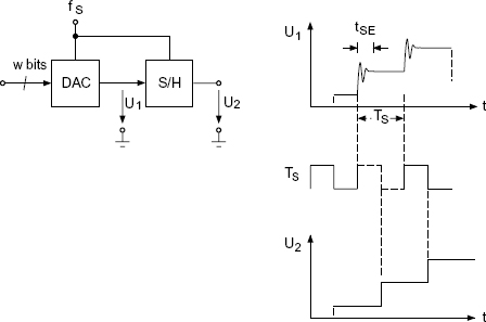
Figure 3.38 Settling time and sample-and-hold function.
Offset and Gain Error. The offset and gain errors of a DA converter are shown in Fig. 3.39.
Differential Nonlinearity. The differential nonlinearity for DA converters describes the step size error of a code word in LSB units. For ideal quantization, the increase Δx of the output voltage until the next code word corresponding to the output voltage is equal to the quantization step size Q (see Fig. 3.40). The difference between two consecutive input codes is termed ΔxQ. Differential nonlinearity is given by

Figure 3.39 Offset and gain error.

Figure 3.40 Differential nonlinearity.
For the code steps from 001 to 010 as shown in Fig. 3.40, the step size is 1.5 LSB, and therefore the differential nonlinearity DNL = 0.5 LSB. The step size between the codes 010 and 100 is 0.75 LSB and DNL = −0.25. The step size for the code change from 011 to 100 is 0 LSB (DNL = −1 LSB).
Integral Nonlinearity. The integral nonlinearity describes the maximum deviation of the output voltage of a real DA converter from the ideal straight line (see Fig. 3.41).
Monotonicity. The continuous increase in the output voltage with increasing input code and the continuous decrease in the output voltage with decreasing input code is called monotonicity. A non-monotonic behavior is presented in Fig. 3.42.

Figure 3.41 Integral nonlinearity.

3.3.2 Switched Voltage and Current Sources
Switched Voltage Sources. The DA conversion with switched voltage sources shown in Fig. 3.43a is carried out with a reference voltage connected to a resistor network. The resistor network consists of 2w resistors of equal resistance and is switched in stages to a binary-controlled decoder so that, at the output, a voltage U2 is present corresponding to the input code. Figure 3.43b shows the decoder for a 3-bit input code 101.
Switched Current Sources. DA conversion with 2w switched current sources is shown in Fig. 3.44. The decoder switches the corresponding number of current sources onto the current-voltage converter. The advantage of both techniques is the monotonicity which is guaranteed for ideal switches but also for slightly deviating resistances. The large number of resistors in switched current sources or the large number of switched current sources causes problems for long word-lengths. The techniques are used in combination with other methods for DA conversion of higher significant bits.
3.3.3 Weighted Resistors and Capacitors
A reduction in the number of identical resistors or current sources is achieved with the following method.

Figure 3.43 Switched voltage sources.

Figure 3.44 Switched current sources.
Weighted Resistors. DA conversion with w switched current sources which are weighted according to
is shown in Fig. 3.45. The output voltage is
where bn takes values 0 or 1. The implementation of DA conversion with switched current sources is carried out with weighted resistors as shown in Fig. 3.46. The output voltage is
Weighted Capacitors. DA conversion with weighted capacitors is shown in Fig. 3.47. During the first phase (switch position 1 in Fig. 3.47) all capacitors are discharged. During the second phase, all capacitors that belong to 1 bit are connected to a reference voltage. Those capacitors belonging to 0 bits are connected to ground. The charge on the capacitors Ca that are connected with the reference voltage can be set equal to the total charge on all capacitors Cg, which leads to

Figure 3.45 Weighted current sources.

Figure 3.46 DA conversion with weighted resistors.
Hence, the output voltage is

Figure 3.47 DA conversion with weighted capacitors.
3.3.4 R-2R Resistor Networks
The DA conversion with switched current sources can also be carried out with an R-2R resistor network as shown in Fig. 3.48. In contrast to the method with weighted resistors, the ratio of the smallest to largest resistor is reduced to 2:1.

Figure 3.48 Switched current sources with R-2R resistor network.
The weighting of currents is achieved by a current division at every junction. Looking right from every junction, a resulting resistance R + 2R ![]() 2R = 2R is found which is equal to the resistance in the vertical direction downwards from the junction. For the current from junction 1 it follows that I1 = UR/2R, and for the current from junction 2 I2 = I1/2. Hence, a binary weighting of the w currents is given by
2R = 2R is found which is equal to the resistance in the vertical direction downwards from the junction. For the current from junction 1 it follows that I1 = UR/2R, and for the current from junction 2 I2 = I1/2. Hence, a binary weighting of the w currents is given by
The output voltage U2 can be written as
3.3.5 Delta-sigma DA Converter
A delta-sigma DA converter is shown in Fig. 3.49. The converter is provided with w-bit data words by an input register with the sampling rate fS. This is followed by a sample rate conversion up to LfS by upsampling and a digital low-pass filter. A delta-sigma modulator converts the w-bit input signal into a 1-bit output signal. The delta-sigma modulator corresponds to the model in Section 3.1.3. Subsequently, the DA conversion of the 1-bit signal is performed followed by the reconstruction of the time-continuous signal by an analog low-pass filter.
3.4 Java Applet – Oversampling and Quantization
The applet shown in Fig. 3.50 demonstrates the influence of oversampling on power spectral density of the quantization error. For a given quantization word-length the noise level can be reduced by changing the oversampling factor. The graphical interface of this applet presents several quantization and oversampling values; these can be used to experiment the noise reduction level. An additional FFT spectral representation provides a visualization of this audio effect.

Figure 3.49 Delta-sigma DA converter.

Figure 3.50 Java applet – oversampling and quantization.
The following functions can be selected on the lower right of the graphical user interface:
- Quantizer
- – word-length w leads to quantization step size Q = 2w−1.
- Dither
- – rect dither – uniform probability density function
- – tri dither – triangular probability density function
- – high-pass dither – triangular probability density function and high-pass power spectral density.
- Noise shaping
- – first-order H(z) = z−1.
- Oversampling factor
- – Factors from 4 up to 64 can be tested depending on the CPU performance of your machine.
You can choose between two predefined audio files from our web server (audio1.wav or audio2.wav) or your own local wav file to be processed [Gui05].
3.5 Exercises
1. Oversampling
- How do we define the power spectral density SXX(ejΩ) of a signal x(n)?
- What is the relationship between signal power
 (variance) and power spectral density SXX(ejΩ)?
 - Why do we need to oversample a time-domain signal?
- Explain why an oversampled PCM A/D converter has lower quantization noise power in the base-band than a Nyquist rate sampled PCM A/D converter.
- How do we perform oversampling by a factor of L in the time domain?
- Explain the frequency-domain interpretation of the oversampling operation.
- What is the pass-band and stop-band frequency of the analog anti-aliasing filter?
- What is the pass-band and stop-band frequency of the digital anti-aliasing filter before downsampling?
- How is the downsampling operation performed (time-domain and frequency-domain explanation)?
2. Delta-sigma Conversion
- Why can we apply noise shaping in an oversampled AD converter?
- Show how the delta-sigma converter (DSC) has a lower quantization error power in the base-band than an oversampled PCM A/D converter.
- How do the power spectral density and variance change in relation to the order of the DSC?
- How is noise shaping achieved in an oversampled delta-sigma AD converter?
- Show the noise shaping effect (with Matlab plots) of a delta sigma modulator and how the improvement of the signal-to-noise for pure oversampling and delta-sigma modulator is achieved.
- Using the previous Matlab plots, specify which order and oversampling factor L will be needed for a 1-bit delta-sigma converter for SNR = 100 dB.
- What is the difference between the delta-sigma modulator in the delta-sigma AD converter and the delta-sigma DA converter?
- How do we achieve a w-bit signal representation at Nyquist sampling frequency from an oversampled 1-bit signal?
- Why do we need to oversample a w-bit signal for a delta-sigma DA converter?
References
[Can85] J. C. Candy: A Use of Double Integration in Sigma Delta Modulation, IEEE Trans. Commun., Vol. COM-37, pp. 249–258, March 1985.
[Can92] J. C. Candy, G. C. Temes, Ed.: Oversampling Delta-Sigma Data Converters, IEEE Press, Piscataway, NJ, 1992.
[Cha90] K. Chao et al: A High Order Topology for Interpolative Modulators for Oversampling A/D Converters, IEEE Trans. Circuits and Syst., Vol. CAS-37, pp. 309–318, March 1990.
[Cro83] R. E. Crochiere, L. R. Rabiner: Multirate Digital Signal Processing, Prentice Hall, Englewood Cliffs, NJ, 1983.
[Fli00] N. Fliege: Multirate Digital Signal Processing, John Wiley & Sons, Ltd, Chichester, 2000.
[Gui05] M. Guillemard, C. Ruwwe, U. Zölzer: J-DAFx – Digital Audio Effects in Java, Proc. 8th Int. Conference on Digital Audio Effects (DAFx-05), pp. 161–166, Madrid, 2005.
[Ino63] H. Inose, Y. Yasuda: A Unity Bit Coding Method by Negative Feedback, Proc. IEEE, Vol. 51, pp. 1524–1535, November 1963.
[Mat87] Y. Matsuya et al: A 16-bit Oversampling A-to-D Conversion Technology Using Triple-Integration Noise Shaping, IEEE J. Solid-State Circuits, Vol. SC-22, pp. 921–929, December 1987.
[She86] D. H. Sheingold, Ed.: Analog-Digital Conversion Handbook, 3rd edn, Prentice Hall, Englewood Cliffs, NJ, 1986.
[Vai93] P. P. Vaidyanathan: Multirate Systems and Filter Banks, Prentice Hall, Englewood Cliffs, NJ, 1993.