
Chapter 4
Audio Processing Systems
Digital signal processors (DSPs) are used for discrete-time signal processing. Their architecture and instruction set is specially designed for real-time processing of signal processing algorithms. DSPs of different manufacturers and their use in practical circuits will be discussed. The restriction to the architecture and practical circuits will provide the user with the criteria necessary for selecting a DSP for a particular application. From the architectural features of different DSPs, the advantages of a certain processor with respect to fast execution of algorithms (digital filter, adaptive filter, FFT, etc.) automatically result. The programming methods and application programs are not dealt with here, because the DSP user guides from different manufacturers provide adequate information in the form of sample programs for a variety of signal processing algorithms.
After comparing DSPs with other microcomputers, the following topics will be discussed in the forthcoming sections:
- fixed-point DSPs;
- floating-point DSPs;
- development tools;
- single-processor systems (peripherals, control principles);
- multi-processor systems (coupling principles, control principles).
The internal design of microcomputers is mainly based on two architectures; the von Neumann architecture which uses a shared instruction/data bus; and the Harvard architecture which has separate buses for instructions and data. Processors based on these architectures are CISCs, RISCs and DSPs. Their characteristics are given in Table 4.1. Besides the internal properties listed in the table, DSPs have special on-chip peripherals which are suited to signal processing applications. The fast response to external interrupts enables their use in real-time operating systems.
| Type | Characteristics |
| CISC | Complex Instruction Set Computer
|
| RISC | Reduced Instruction Set Computer
|
| DSP | Digital Signal Processor
|
4.1 Digital Signal Processors
4.1.1 Fixed-point DSPs
The discrete-time and discrete-amplitude output of an AD converter is usually represented in 2's complement format. The processing of these number sequences is carried out with fixed-point or floating-point arithmetic. The output of a processed signal is again in 2's complement format and is fed to a DA converter. The signed fractional representation (2's complement) is the common method for algorithms in fixed-point number representation. For address generation and modulo operations unsigned integers are used. Figure 4.1 shows a schematic diagram of a typical fixed-point DSP. The main building blocks are program controller, arithmetic logic unit (ALU) with a multiplier-accumulator (MAC), program and data memory and interfaces to external memory and peripherals. All blocks are connected with each other by an internal bus system. The internal bus system has separate instruction and data buses. The data bus itself can consist of more than one parallel bus enabling it, for instance, to transmit both operands of a multiplication instruction to the MAC in parallel. The internal memory consists of instruction and data RAM and additional ROM memory. This internal memory permits fast execution of internal instructions and data transfer. For increasing memory space, address/control and data buses are connected to external memories like EPROM, ROM and RAM. The connection of the external bus system to the internal bus architecture has great influence on efficient execution of external instructions as well as on processing external data. In order to connect serially operating AD/DA converters, special serial interfaces with high transmission rates are offered by several DSPs. Moreover, some processors support direct connection to an RS232 interface. The control from a microprocessor can be achieved via a host interface with a word-length of 8 bits.

Figure 4.1 Schematic diagram of a fixed-point DSP.
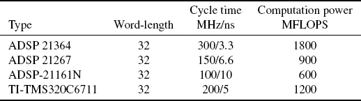
An overview of fixed-point DSPs with respect to word-length and cycle time is shown in Table 4.2. Basically, the precision of the arithmetic can be doubled if quantization affects the stability and numeric precision of the applied algorithm. The cycle time in connection with processing time (in processor cycles) of a combined multiplication and accumulation command gives insight into the computing power of a particular processor type. The cycle time directly results from the maximum clock frequency. The instruction processing time depends mainly on the internal instruction and data structure as well as on the external memory connections of the processor. The fast access to external instruction and data memories is of special significance in complex algorithms and in processing huge data loads. Further attention has to be paid to the linking of serial data connections with AD/DA converters and the control by a host computer over a special host interface. Complex interface circuits could therefore be avoided. For stand-alone solutions, program loading from a simple external EPROM can also be done.
For signal processing algorithms, the following software commands are necessary:
- MAC (multiply and accumulate) → combined multiplication and addition command;
- simultaneous transfer of both operands for multiplication to the MAC (parallel move);
- bit-reversed addressing (for FFT);
- modulo addressing (for windowing and filtering).
Different signal processors have different processing times for FFT implementations. The latest signal processors with improved architecture have shorter processing times. The instruction cycles for the combined multiplication and accumulation command (application: windowing, filtering) are approximately equal for different processors, but processing cycles for external operands have to be considered.
Table 4.2 Fixed-point DSPs (Analog Devices AD, Texas Instruments TI, Motorola MOT, Agere Systems AG).

4.1.2 Floating-point DSPs
Figure 4.2 shows the block diagram of a typical floating-point DSP. The main characteristics of the different architectures are the dual-port principle (Motorola, Texas Instruments) and the external Harvard architecture (Analog Devices, NEC). Floating-point DSPs internally have multiple bus systems in order to accelerate data transfer to the processing unit. An on-chip DMA controller and cache memory support higher data transfer rates. An overview of floating-point DSPs is shown in Table 4.3. Besides the standardized floating-point representation IEEE-754, there are also manufacturer-dependent number representations.

Figure 4.2 Block diagram of a floating-point digital signal processor.
Table 4.3 Floating-point DSPs.
4.2 Digital Audio Interfaces
For transferring digital audio signals, two transmission standards have been established by the AES (Audio Engineering Society) and the EBU (European Broadcasting Union), respectively. These standards are for two-channel transmission [AES92] and for multichannel transmission of up to 56 audio signals.

Figure 4.3 Two-channel format.

Figure 4.4 Two-channel format (subframe).
4.2.1 Two-channel AES/EBU Interface
For the two-channel AES/EBU interface, professional and consumer modes are defined. The outer frame is identical for both modes and is shown in Fig. 4.3. For a sampling period a frame is defined so that it consists of two subframes, for channel 1 with preamble X, and for channel 2 with preamble Y. A total of 192 frames form a block, and the block start is characterized by a special preamble Z. The bit allocation of a subframe consists of 32 bits as in Fig. 4.4. The preamble consists of 4 bits (bit 0,…, 3) and the audio data of up to 24 bits (bit 4, …, 27). The last four bits of the subframe characterize Validity (validity of data word or error), User Status (usable bit), Channel Status (from 192 bits/block = 24 bytes coded status information for the channel) and Parity (even parity). The transmission of the serial data bits is carried out with a biphase code. This is done with the help of an XOR relationship between clock (of double bit rate) and the serial data bits (Fig. 4.5). At the receiver, clock retrieval is achieved by detecting the preamble (X = 11100010, Y = 11100100, Z = 11101000) as it violates the coding rule (see Fig. 4.6). The meaning of the 24 bytes for channel status information is summarized in Table 4.4. An exact bit allocation of the first three important bytes of this channel status information is presented in Fig. 4.7. In the individual fields of byte 0, preemphasis and sampling rate are specified besides professional/consumer modes and the characterization of data/audio (see Tables 4.5 and 4.6). Byte 1 determines the channel mode (Table 4.7). The consumer format (often labeled SPDIF = Sony/Philips Digital Interface Format) differs from the professional format in the definition of the channel status information and the technical specifications for inputs and outputs. The bit allocation for the first four bits of the channel information is shown in Fig. 4.8. For consumer applications, two-wired leads with RCA connectors are used. The inputs and outputs are asymmetrical. Also, optical connectors exist. For professional use, shielded two-wired leads with XLR connectors and symmetrical inputs and outputs (professional format) are used. Table 4.8 shows the electrical specifications for professional AES/EBU interfaces.


4.2.2 MADI Interface
For connecting an audio processing system at different locations, a MADI interface (Multichannel Audio Digital Interface) is used. A system link by MADI is presented in Fig. 4.9. Analog/digital I/O systems consisting of AD/DA converters, AES/EBU interfaces (AES) and sampling rate converters (SRC) are connected to digital distribution systems with bi-directional MADI links. The actual audio signal processing is performed in special DSP systems which are connected to the digital distribution systems by MADI links. The MADI format is derived from the two-channel AES/EBU format and allows the transmission of 56 digital mono channels (see Fig. 4.10) within a sampling period. The MADI frame consists of 56 AES/EBU subframes. Each channel has a preamble containing the information shown in Fig. 4.10. The bit 0 is responsible for identifying the first MADI channel (MADI Channel 0). Table 4.9 shows the sampling rates and the corresponding data transfer rates. The maximum data rate of 96.768 Mbit/s is required at sampling rate of 48 kHz + 12.5%. Data transmission is done by FDDI techniques (Fiber Distributed Digital Interface). The transmission rate of 125 Mbit/s is implemented with special TAXI chips. The transmission for a coaxial cable is already specified (see Table 4.10). The optical transmission medium for audio applications is not yet defined.
Table 4.4 Channel status bytes.
| Byte | Description |
| 0 | Emphasis, sampling rate |
| 1 | Channel use |
| 2 | Sample length |
| 3 | Vector for byte 1 |
| 4 | Reference bits |
| 5 | Reserved |
| 6–9 | 4 bytes of ASCII origin |
| 10–13 | 4 bytes of ASCII destination |
| 14–17 | 4 bytes of local address |
| 18–21 | Time code |
| 22 | Flags |
| 23 | CRC |

Figure 4.7 Bytes 0–2 of channel status information.
| 0 | None indicated, override enabled |
| 4 | None indicated, override disabled |
| 6 | 50/15 µs emphasis |
| 7 | CCITT J.17 emphasis |
Table 4.6 Sampling rate field.
| 0 | None indicated (48 kHz default) |
| 1 | 48 kHz |
| 2 | 44.1 kHz |
| 3 | 32 kHz |
| 0 | None indicated (2 channel default) |
| 1 | Two channel |
| 2 | Monaural |
| 3 | Primary/secondary (A = primary, B = secondary) |
| 4 | Stereo (A = left, B = right) |
| 7 | Vector to byte 3 |

Figure 4.8 Bytes 0–3 (consumer format).
Table 4.8 Electrical specifications of professional interfaces.
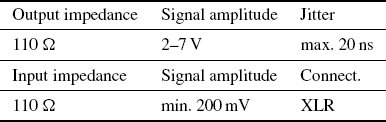
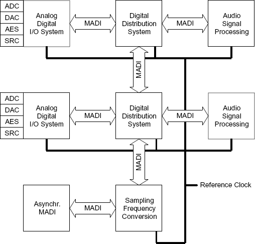
Figure 4.9 A system link by MADI.
Table 4.9 MADI specifications.
| Sampling rate | 32 kHz–48 kHz ± 12.5% |
| Transmission rate | 125 Mbit/s |
| Data transfer rate | 100 Mbit/s |
| Max. data transfer rate | 96.768 Mbit/s (56 channels at 48 kHz + 12.5%) |
| Min. data transfer rate | 50.176 Mbit/s (56 channels at 32 kHz − 12.5%) |
A unidirectional MADI link is shown in Fig. 4.11. The MADI transmitter and receiver must be synchronized by a common master clock. The transmission between FDDI chips is performed by a transmitter with integrated clock generation and clock retrieval at the receiver.

Figure 4.10 MADI frame format.
Table 4.10 Electrical specifications (MADI).


4.3 Single-processor Systems
4.3.1 Peripherals
A common system configuration is shown in Fig. 4.12. It consists of a DSP, clock generation, instruction and data memory and a BOOT-EPROM. After RESET, the program is loaded into the internal RAM of the signal processor. The loading is done byte by byte so that only an EPROM with 8-bit data word-length is necessary. In terms of circuit complexity the connection of AD/DA converters over serial interfaces is the simplest solution. Most fixed-point signal processors support serial connection where a lead ‘connection’ for bit clock SCLK, sampling clock/word clock WCLK, and the serial input and output data SDRX/SDTX are used. The clock signals are obtained from a higher reference clock CLKIN (see Fig. 4.13). For non-serially operating AD/DA converters, parallel interfaces can also be connected to the DSP.
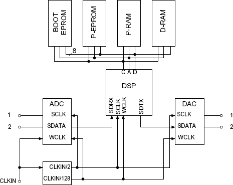
Figure 4.12 DSP system with two-channel AD/DA converters (C = control, A = address, D = data, SDATA = serial data, SCLK = bit clock, WCLK = word clock, SDRX = serial input, SDTX = serial output).
4.3.2 Control
For controlling digital signal processors and data exchange with host processors, some DSPs provide a special host interface that can be read and written directly (see Fig. 4.14). The data word-length depends on the processor. The host interface is included in the external address space of the host or is connected to a local bus system, for instance a PC bus.
A DSP as a coprocessor for special signal processing problems can be used by connecting it with a dual-port RAM and additional interrupt logic to a host processor. This enables data transmission between the DSP system and host processor (see Fig. 4.15). This results in a complete separation from the host processor. The communication can either be interrupt-controlled or carried out by polling a memory address in a dual-port RAM.
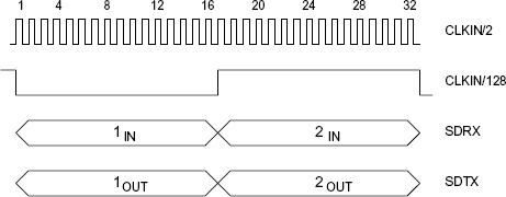
Figure 4.13 Serial transmission format.

Figure 4.14 Control via a host interface of the DSP (CS = chip select, R/![]() = read / write, A = address, D = data).
= read / write, A = address, D = data).
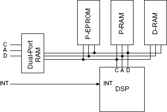
Figure 4.15 Control over a dual-port RAM and interrupt.
A very simple control can be done directly via an RS232-interface. This is can be carried out via an additional asynchronous serial interface (Serial Communication Interface) of the DSP (see Fig. 4.16).
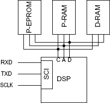
Figure 4.16 Control over a serial interface (RS232, RS422).

Figure 4.17 Cascading and pipelining (SDATA = serial data, SCLK = bit clock, SYNC = synchronization).

Figure 4.18 Parallel configuration with output time-multiplex.

Figure 4.19 Time-multiplex connection (ADR = address at a particular time).
4.4 Multi-processor Systems
The design of multi-processor systems can be carried out by linking signal processors by serial or parallel interfaces. Besides purely multi-processor DSP systems, an additional connection to standard bus systems can be made as well.
![]()
Figure 4.20 Cascading and pipelining.

Figure 4.21 Parallel configuration.

Figure 4.22 Connection over a four-port RAM.

Figure 4.23 Signal processor systems based on standard bus system.
4.4.1 Connection via Serial Links
In connecting via serial links, signal processors are cascaded so that different program segments are distributed over different processors (see Fig. 4.17). The serial output data is fed into the serial input of the following signal processor. A synchronous bit clock and a common synchronization SYNC control the serial interface. With the help of a serial time-multiplex mode (Fig. 4.18) a parallel configuration can be designed which, for instance, feeds several parallel signal processors with serial input data. The serial outputs of signal processors provide output data in time-multiplex. A complete time-multiplex connection via the serial interface of the signal processor is shown in Fig. 4.19. The allocation of a signal processor at a particular time slot can either be fixed or carried out by an address control ADR.

4.4.2 Connection via Parallel Links
Connection via parallel links is possible with dual-port processors as well as with dual-port RAMs (see Fig. 4.20). A parallel configuration of signal processor systems with a local bus is shown in Fig. 4.21. The connection to the local bus is done either over a dual-port RAM or directly with a second signal processor port. Another possible configuration is the use of a four-port RAM as shown in Fig. 4.22. Here, one processor serves as a connector to a system bus and feeds three other processors over a four-port RAM with control and data information.

Figure 4.25 Scalable digital audio system.
4.4.3 Connection via Standard Bus Systems
The use of standard bus systems (VME bus, MULTIBUS, PC bus) to control multi-processor systems is presented in Fig. 4.23. The connection of signal processors can either be carried out directly over a control bus or with the help of a special data bus. This parallel data bus can operate in time-multiplex. Hence, control information and data are separated. A few of the criteria for standard bus systems are data transfer rate, interrupt request and processing, the option of several masters, auxiliary functions (power supply, bus error, battery buffer) and mechanical requirements.
4.4.4 Scalable Audio System
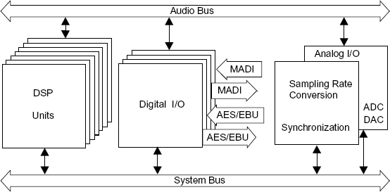
The functional segmentation of an audio system into different stages, the analog, interface, digital and man – machine stages, is shown in Fig. 4.24. All stages are controlled by a LAN (Local Area Network). In the analog domain, crosspoint switches and microphone amplifiers are controlled. In the interface domain AD/DA converters and sampling rate converters are used. The connection to a signal processing system is done by AES/EBU and MADI interfaces. A host computer with a control console for the sound engineer serves as the central control unit.
The realization of the digital domain with the help of a standard bus system is shown in Fig. 4.25. A central mixing console controls several subsystems over a host. These subsystems have special control computers which control several DSP modules. The system concept is scalable within a subsystem and by extension to several subsystems. Audio data transfer between subsystems is performed by AES/EBU and MADI interfaces. The segmentation within a subsystem is shown in Fig. 4.26. Here, besides DSP modules, digital interfaces (AES/EBU, MADI, sampling rate converters, etc.) and AD/DA converters can be integrated.
References
[AES91] AES10-1991 (ANSI S4.43-1991): AES Recommended Practice for Digital Audio Engineering – Serial Multichannel Audio Digital Interface (MADI).
[AES92] AES3-1992 (ANSI S4.40-1992): AES Recommended Practice for Digital Audio Engineering – Serial Transmission Format for Two-Channel Linearly Represented Digital Audio.