B Review of Memory Hierarchy
Cache: a safe place for hiding or storing things.
B.1 Introduction
This appendix is a quick refresher of the memory hierarchy, including the basics of cache and virtual memory, performance equations, and simple optimizations. This first section reviews the following 36 terms:
| cache | fully associative | write allocate |
| virtual memory | dirty bit | unified cache |
| memory stall cycles | block offset | misses per instruction |
| direct mapped | write-back | block |
| valid bit | data cache | locality |
| block address | hit time | address trace |
| write-through | cache miss | set |
| instruction cache | page fault | random replacement |
| average memory access time | miss rate | index field |
| cache hit | n-way set associative | no-write allocate |
| page | least recently used | write buffer |
| miss penalty | tag field | write stall |
If this review goes too quickly, you might want to look at Chapter 7 in Computer Organization and Design, which we wrote for readers with less experience.
Cache is the name given to the highest or first level of the memory hierarchy encountered once the address leaves the processor. Since the principle of locality applies at many levels, and taking advantage of locality to improve performance is popular, the term cache is now applied whenever buffering is employed to reuse commonly occurring items. Examples include file caches, name caches, and so on.
When the processor finds a requested data item in the cache, it is called a cache hit. When the processor does not find a data item it needs in the cache, a cache miss occurs. A fixed-size collection of data containing the requested word, called a block or line run, is retrieved from the main memory and placed into the cache. Temporal locality tells us that we are likely to need this word again in the near future, so it is useful to place it in the cache where it can be accessed quickly. Because of spatial locality, there is a high probability that the other data in the block will be needed soon.
The time required for the cache miss depends on both the latency and bandwidth of the memory. Latency determines the time to retrieve the first word of the block, and bandwidth determines the time to retrieve the rest of this block. A cache miss is handled by hardware and causes processors using in-order execution to pause, or stall, until the data are available. With out-of-order execution, an instruction using the result must still wait, but other instructions may proceed during the miss.
Similarly, not all objects referenced by a program need to reside in main memory. Virtual memory means some objects may reside on disk. The address space is usually broken into fixed-size blocks, called pages. At any time, each page resides either in main memory or on disk. When the processor references an item within a page that is not present in the cache or main memory, a palt occurs, and the entire page is moved from the disk to main memory. Since page faults take so long, they are handled in software and the processor is not stalled. The processor usually switches to some other task while the disk access occurs. From a high-level perspective, the reliance on locality of references and the relative relationships in size and relative cost per bit of cache versus main memory are similar to those of main memory versus disk.
Figure B.1 shows the range of sizes and access times of each level in the memory hierarchy for computers ranging from high-end desktops to low-end servers.

Figure B.1 The typical levels in the hierarchy slow down and get larger as we move away from the processor for a large workstation or small server. Embedded computers might have no disk storage and much smaller memories and caches. The access times increase as we move to lower levels of the hierarchy, which makes it feasible to manage the transfer less responsively. The implementation technology shows the typical technology used for these functions. The access time is given in nanoseconds for typical values in 2006; these times will decrease over time. Bandwidth is given in megabytes per second between levels in the memory hierarchy. Bandwidth for disk storage includes both the media and the buffered interfaces.
Cache Performance Review
Because of locality and the higher speed of smaller memories, a memory hierarchy can substantially improve performance. One method to evaluate cache performance is to expand our processor execution time equation from Chapter 1. We now account for the number of cycles during which the processor is stalled waiting for a memory access, which we call the memory stall cycles. The performance is then the product of the clock cycle time and the sum of the processor cycles and the memory stall cycles:
This equation assumes that the CPU clock cycles include the time to handle a cache hit and that the processor is stalled during a cache miss. Section B.2 reexamines this simplifying assumption.
The number of memory stall cycles depends on both the number of misses and the cost per miss, which is called the miss penalty:

The advantage of the last form is that the components can be easily measured. We already know how to measure instruction count (IC). (For speculative processors, we only count instructions that commit.) Measuring the number of memory references per instruction can be done in the same fashion; every instruction requires an instruction access, and it is easy to decide if it also requires a data access.
Note that we calculated miss penalty as an average, but we will use it below as if it were a constant. The memory behind the cache may be busy at the time of the miss because of prior memory requests or memory refresh. The number of clock cycles also varies at interfaces between different clocks of the processor, bus, and memory. Thus, please remember that using a single number for miss penalty is a simplification.
The component miss rate is simply the fraction of cache accesses that result in a miss (i.e., number of accesses that miss divided by number of accesses). Miss rates can be measured with cache simulators that take an address trace of the instruction and data references, simulate the cache behavior to determine which references hit and which miss, and then report the hit and miss totals. Many microprocessors today provide hardware to count the number of misses and memory references, which is a much easier and faster way to measure miss rate.
The formula above is an approximation since the miss rates and miss penalties are often different for reads and writes. Memory stall clock cycles could then be defined in terms of the number of memory accesses per instruction, miss penalty (in clock cycles) for reads and writes, and miss rate for reads and writes:
We normally simplify the complete formula by combining the reads and writes and finding the average miss rates and miss penalty for reads and writes:
The miss rate is one of the most important measures of cache design, but, as we will see in later sections, not the only measure.
Example
Assume we have a computer where the cycles per instruction (CPI) is 1.0 when all memory accesses hit in the cache. The only data accesses are loads and stores, and these total 50% of the instructions. If the miss penalty is 25 clock cycles and the miss rate is 2%, how much faster would the computer be if all instructions were cache hits?
Answer
First compute the performance for the computer that always hits:

Now for the computer with the real cache, first we compute memory stall cycles:

where the middle term (1 + 0.5) represents one instruction access and 0.5 data accesses per instruction. The total performance is thus
The performance ratio is the inverse of the execution times:

Some designers prefer measuring miss rate as misses per instruction rather than misses per memory reference. These two are related:
The latter formula is useful when you know the average number of memory accesses per instruction because it allows you to convert miss rate into misses per instruction, and vice versa. For example, we can turn the miss rate per memory reference in the previous example into misses per instruction:
By the way, misses per instruction are often reported as misses per 1000 instructions to show integers instead of fractions. Thus, the answer above could also be expressed as 30 misses per 1000 instructions.
The advantage of misses per instruction is that it is independent of the hardware implementation. For example, speculative processors fetch about twice as many instructions as are actually committed, which can artificially reduce the miss rate if measured as misses per memory reference rather than per instruction. The drawback is that misses per instruction is architecture dependent; for example, the average number of memory accesses per instruction may be very different for an 80×86 versus MIPS. Thus, misses per instruction are most popular with architects working with a single computer family, although the similarity of RISC architectures allows one to give insights into others.

Four Memory Hierarchy Questions
We continue our introduction to caches by answering the four common questions for the first level of the memory hierarchy:
The answers to these questions help us understand the different trade-offs of memories at different levels of a hierarchy; hence, we ask these four questions on every example.
Q1: Where Can a Block Be Placed in a Cache?
Figure B.2 shows that the restrictions on where a block is placed create three categories of cache organization:

Figure B.2 This example cache has eight block frames and memory has 32 blocks. The three options for caches are shown left to right. In fully associative, block 12 from the lower level can go into any of the eight block frames of the cache. With direct mapped, block 12 can only be placed into block frame 4 (12 modulo 8). Set associative, which has some of both features, allows the block to be placed anywhere in set 0 (12 modulo 4). With two blocks per set, this means block 12 can be placed either in block 0 or in block 1 of the cache. Real caches contain thousands of block frames, and real memories contain millions of blocks. The set associative organization has four sets with two blocks per set, called two-way set associative. Assume that there is nothing in the cache and that the block address in question identifies lower-level block 12.
If there are n blocks in a set, the cache placement is called n-way set associative.
The range of caches from direct mapped to fully associative is really a continuum of levels of set associativity. Direct mapped is simply one-way set associative, and a fully associative cache with m blocks could be called “m- way set associative.” Equivalently, direct mapped can be thought of as having m sets, and fully associative as having one set.
The vast majority of processor caches today are direct mapped, two-way set associative, or four-way set associative, for reasons we will see shortly.
Q2: How Is a Block Found If It Is in the Cache?
Caches have an address tag on each block frame that gives the block address. The tag of every cache block that might contain the desired information is checked to see if it matches the block address from the processor. As a rule, all possible tags are searched in parallel because speed is critical.
There must be a way to know that a cache block does not have valid information. The most common procedure is to add a valid bit to the tag to say whether or not this entry contains a valid address. If the bit is not set, there cannot be a match on this address.
Before proceeding to the next question, let’s explore the relationship of a processor address to the cache. Figure B.3 shows how an address is divided. The first division is between the block address and the block offset. The block frame address can be further divided into the tag field and the index field. The block offset field selects the desired data from the block, the index field selects the set, and the tag field is compared against it for a hit. Although the comparison could be made on more of the address than the tag, there is no need because of the following:
Figure B.3 The three portions of an address in a set associative or direct-mapped cache. The tag is used to check all the blocks in the set, and the index is used to select the set. The block offset is the address of the desired data within the block. Fully associative caches have no index field.
If the total cache size is kept the same, increasing associativity increases the number of blocks per set, thereby decreasing the size of the index and increasing the size of the tag. That is, the tag-index boundary in Figure B.3 moves to the right with increasing associativity, with the end point of fully associative caches having no index field.
Q3: Which Block Should Be Replaced on a Cache Miss?
When a miss occurs, the cache controller must select a block to be replaced with the desired data. A benefit of direct-mapped placement is that hardware decisions are simplified—in fact, so simple that there is no choice: Only one block frame is checked for a hit, and only that block can be replaced. With fully associative or set associative placement, there are many blocks to choose from on a miss. There are three primary strategies employed for selecting which block to replace:
A virtue of random replacement is that it is simple to build in hardware. As the number of blocks to keep track of increases, LRU becomes increasingly expensive and is usually only approximated. A common approximation (often called pseudo-LRU) has a set of bits for each set in the cache with each bit corresponding to a single way (a way is bank in a set associative cache; there are four ways in four-way set associative cache) in the cache. When a set is accessed, the bit corresponding to the way containing the desired block is turned on; if all the bits associated with a set are turned on, they are reset with the exception of the most recently turned on bit. When a block must be replaced, the processor chooses a block from the way whose bit is turned off, often randomly if more than one choice is available. This approximates LRU, since the block that is replaced will not have been accessed since the last time that all the blocks in the set were accessed. Figure B.4 shows the difference in miss rates between LRU, random, and FIFO replacement.

Figure B.4 Data cache misses per 1000 instructions comparing least recently used, random, and first in, first out replacement for several sizes and associativities. There is little difference between LRU and random for the largest size cache, with LRU outperforming the others for smaller caches. FIFO generally outperforms random in the smaller cache sizes. These data were collected for a block size of 64 bytes for the Alpha architecture using 10 SPEC2000 benchmarks. Five are from SPECint2000 (gap, gcc, gzip, mcf, and perl) and five are from SPECfp2000 (applu, art, equake, lucas, and swim). We will use this computer and these benchmarks in most figures in this appendix.
Q4: What Happens on a Write?
Reads dominate processor cache accesses. All instruction accesses are reads, and most instructions don’t write to memory. Figures A.32 and A.33 in Appendix A suggest a mix of 10% stores and 26% loads for MIPS programs, making writes 10%/(100% + 26% + 10%) or about 7% of the overall memory traffic. Of the data cache traffic, writes are 10%/(26% + 10%) or about 28%. Making the common case fast means optimizing caches for reads, especially since processors traditionally wait for reads to complete but need not wait for writes. Amdahl’s law (Section 1.9) reminds us, however, that high-performance designs cannot neglect the speed of writes.
Fortunately, the common case is also the easy case to make fast. The block can be read from the cache at the same time that the tag is read and compared, so the block read begins as soon as the block address is available. If the read is a hit, the requested part of the block is passed on to the processor immediately. If it is a miss, there is no benefit—but also no harm except more power in desktop and server computers; just ignore the value read.
Such optimism is not allowed for writes. Modifying a block cannot begin until the tag is checked to see if the address is a hit. Because tag checking cannot occur in parallel, writes normally take longer than reads. Another complexity is that the processor also specifies the size of the write, usually between 1 and 8 bytes; only that portion of a block can be changed. In contrast, reads can access more bytes than necessary without fear.
The write policies often distinguish cache designs. There are two basic options when writing to the cache:
To reduce the frequency of writing back blocks on replacement, a feature called the dirty bit is commonly used. This status bit indicates whether the block is dirty (modified while in the cache) or clean (not modified). If it is clean, the block is not written back on a miss, since identical information to the cache is found in lower levels.
Both write-back and write-through have their advantages. With write-back, writes occur at the speed of the cache memory, and multiple writes within a block require only one write to the lower-level memory. Since some writes don’t go to memory, write-back uses less memory bandwidth, making write-back attractive in multiprocessors. Since write-back uses the rest of the memory hierarchy and memory interconnect less than write-through, it also saves power, making it attractive for embedded applications.
Write-through is easier to implement than write-back. The cache is always clean, so unlike write-back read misses never result in writes to the lower level. Write-through also has the advantage that the next lower level has the most current copy of the data, which simplifies data coherency. Data coherency is important for multiprocessors and for I/O, which we examine in Chapter 4 and Appendix D. Multilevel caches make write-through more viable for the upper-level caches, as the writes need only propagate to the next lower level rather than all the way to main memory.
As we will see, I/O and multiprocessors are fickle: They want write-back for processor caches to reduce the memory traffic and write-through to keep the cache consistent with lower levels of the memory hierarchy.
When the processor must wait for writes to complete during write-through, the processor is said to write stall. A common optimization to reduce write stalls is a write buffer, which allows the processor to continue as soon as the data are written to the buffer, thereby overlapping processor execution with memory updating. As we will see shortly, write stalls can occur even with write buffers.
Since the data are not needed on a write, there are two options on a write miss:
Thus, blocks stay out of the cache in no-write allocate until the program tries to read the blocks, but even blocks that are only written will still be in the cache with write allocate. Let’s look at an example.
Example
Assume a fully associative write-back cache with many cache entries that starts empty. Below is a sequence of five memory operations (the address is in square brackets):
What are the number of hits and misses when using no-write allocate versus write allocate?
Answer
For no-write allocate, the address 100 is not in the cache, and there is no allocation on write, so the first two writes will result in misses. Address 200 is also not in the cache, so the read is also a miss. The subsequent write to address 200 is a hit. The last write to 100 is still a miss. The result for no-write allocate is four misses and one hit.
For write allocate, the first accesses to 100 and 200 are misses, and the rest are hits since 100 and 200 are both found in the cache. Thus, the result for write allocate is two misses and three hits.
Either write miss policy could be used with write-through or write-back. Normally, write-back caches use write allocate, hoping that subsequent writes to that block will be captured by the cache. Write-through caches often use no-write allocate. The reasoning is that even if there are subsequent writes to that block, the writes must still go to the lower-level memory, so what’s to be gained?
An Example: The Opteron Data Cache
To give substance to these ideas, Figure B.5 shows the organization of the data cache in the AMD Opteron microprocessor. The cache contains 65,536 (64K) bytes of data in 64-byte blocks with two-way set associative placement, least-recently used replacement, write-back, and write allocate on a write miss.

Figure B.5 The organization of the data cache in the Opteron microprocessor. The 64 KB cache is two-way set associative with 64-byte blocks. The 9-bit index selects among 512 sets. The four steps of a read hit, shown as circled numbers in order of occurrence, label this organization. Three bits of the block offset join the index to supply the RAM address to select the proper 8 bytes. Thus, the cache holds two groups of 4096 64-bit words, with each group containing half of the 512 sets. Although not exercised in this example, the line from lower-level memory to the cache is used on a miss to load the cache. The size of address leaving the processor is 40 bits because it is a physical address and not a virtual address. Figure B.24 on page B-47 explains how the Opteron maps from virtual to physical for a cache access.
Let’s trace a cache hit through the steps of a hit as labeled in Figure B.5. (The four steps are shown as circled numbers.) As described in Section B.5, the Opteron presents a 48-bit virtual address to the cache for tag comparison, which is simultaneously translated into a 40-bit physical address.
The reason Opteron doesn’t use all 64 bits of virtual address is that its designers don’t think anyone needs that big of a virtual address space yet, and the smaller size simplifies the Opteron virtual address mapping. The designers plan to grow the virtual address in future microprocessors.
The physical address coming into the cache is divided into two fields: the 34-bit block address and the 6-bit block offset (64 = 26 and 34 + 6 = 40). The block address is further divided into an address tag and cache index. Step 1 shows this division.
The cache index selects the tag to be tested to see if the desired block is in the cache. The size of the index depends on cache size, block size, and set associativity. For the Opteron cache the set associativity is set to two, and we calculate the index as follows:
Hence, the index is 9 bits wide, and the tag is 34 – 9 or 25 bits wide. Although that is the index needed to select the proper block, 64 bytes is much more than the processor wants to consume at once. Hence, it makes more sense to organize the data portion of the cache memory 8 bytes wide, which is the natural data word of the 64-bit Opteron processor. Thus, in addition to 9 bits to index the proper cache block, 3 more bits from the block offset are used to index the proper 8 bytes. Index selection is step 2 in Figure B.5.
After reading the two tags from the cache, they are compared to the tag portion of the block address from the processor. This comparison is step 3 in the figure. To be sure the tag contains valid information, the valid bit must be set or else the results of the comparison are ignored.
Assuming one tag does match, the final step is to signal the processor to load the proper data from the cache by using the winning input from a 2:1 multiplexor. The Opteron allows 2 clock cycles for these four steps, so the instructions in the following 2 clock cycles would wait if they tried to use the result of the load.
Handling writes is more complicated than handling reads in the Opteron, as it is in any cache. If the word to be written is in the cache, the first three steps are the same. Since the Opteron executes out of order, only after it signals that the instruction has committed and the cache tag comparison indicates a hit are the data written to the cache.
So far we have assumed the common case of a cache hit. What happens on a miss? On a read miss, the cache sends a signal to the processor telling it the data are not yet available, and 64 bytes are read from the next level of the hierarchy. The latency is 7 clock cycles to the first 8 bytes of the block, and then 2 clock cycles per 8 bytes for the rest of the block. Since the data cache is set associative, there is a choice on which block to replace. Opteron uses LRU, which selects the block that was referenced longest ago, so every access must update the LRU bit. Replacing a block means updating the data, the address tag, the valid bit, and the LRU bit.
Since the Opteron uses write-back, the old data block could have been modified, and hence it cannot simply be discarded. The Opteron keeps 1 dirty bit per block to record if the block was written. If the “victim” was modified, its data and address are sent to the victim buffer. (This structure is similar to a write buffer in other computers.) The Opteron has space for eight victim blocks. In parallel with other cache actions, it writes victim blocks to the next level of the hierarchy. If the victim buffer is full, the cache must wait.
A write miss is very similar to a read miss, since the Opteron allocates a block on a read or a write miss.
We have seen how it works, but the data cache cannot supply all the memory needs of the processor: The processor also needs instructions. Although a single cache could try to supply both, it can be a bottleneck. For example, when a load or store instruction is executed, the pipelined processor will simultaneously request both a data word and an instruction word. Hence, a single cache would present a structural hazard for loads and stores, leading to stalls. One simple way to conquer this problem is to divide it: One cache is dedicated to instructions and another to data. Separate caches are found in most recent processors, including the Opteron. Hence, it has a 64 KB instruction cache as well as the 64 KB data cache.
The processor knows whether it is issuing an instruction address or a data address, so there can be separate ports for both, thereby doubling the bandwidth between the memory hierarchy and the processor. Separate caches also offer the opportunity of optimizing each cache separately: Different capacities, block sizes, and associativities may lead to better performance. (In contrast to the instruction caches and data caches of the Opteron, the terms unified or mixed are applied to caches that can contain either instructions or data.)
Figure B.6 shows that instruction caches have lower miss rates than data caches. Separating instructions and data removes misses due to conflicts between instruction blocks and data blocks, but the split also fixes the cache space devoted to each type. Which is more important to miss rates? A fair comparison of separate instruction and data caches to unified caches requires the total cache size to be the same. For example, a separate 16 KB instruction cache and 16 KB data cache should be compared to a 32 KB unified cache. Calculating the average miss rate with separate instruction and data caches necessitates knowing the percentage of memory references to each cache. From the data in Appendix A we find the split is 100%/(100% + 26% + 10%) or about 74% instruction references to (26% + 10%)/(100% + 26% + 10%) or about 26% data references. Splitting affects performance beyond what is indicated by the change in miss rates, as we will see shortly.

Figure B.6 Miss per 1000 instructions for instruction, data, and unified caches of different sizes. The percentage of instruction references is about 74%. The data are for two-way associative caches with 64-byte blocks for the same computer and benchmarks as Figure B.4.
B.2 Cache Performance
Because instruction count is independent of the hardware, it is tempting to evaluate processor performance using that number. Such indirect performance measures have waylaid many a computer designer. The corresponding temptation for evaluating memory hierarchy performance is to concentrate on miss rate because it, too, is independent of the speed of the hardware. As we will see, miss rate can be just as misleading as instruction count. A better measure of memory hierarchy performance is the average memory access time:
where hit time is the time to hit in the cache; we have seen the other two terms before. The components of average access time can be measured either in absolute time—say, 0.25 to 1.0 nanoseconds on a hit—or in the number of clock cycles that the processor waits for the memory—such as a miss penalty of 150 to 200 clock cycles. Remember that average memory access time is still an indirect measure of performance; although it is a better measure than miss rate, it is not a substitute for execution time.
This formula can help us decide between split caches and a unified cache.
Example
Which has the lower miss rate: a 16 KB instruction cache with a 16 KB data cache or a 32 KB unified cache? Use the miss rates in Figure B.6 to help calculate the correct answer, assuming 36% of the instructions are data transfer instructions. Assume a hit takes 1 clock cycle and the miss penalty is 100 clock cycles. A load or store hit takes 1 extra clock cycle on a unified cache if there is only one cache port to satisfy two simultaneous requests. Using the pipelining terminology of Chapter 3, the unified cache leads to a structural hazard. What is the average memory access time in each case? Assume write-through caches with a write buffer and ignore stalls due to the write buffer.
Answer
First let’s convert misses per 1000 instructions into miss rates. Solving the general formula from above, the miss rate is

Since every instruction access has exactly one memory access to fetch the instruction, the instruction miss rate is
Since 36% of the instructions are data transfers, the data miss rate is
The unified miss rate needs to account for instruction and data accesses:
As stated above, about 74% of the memory accesses are instruction references. Thus, the overall miss rate for the split caches is
Thus, a 32 KB unified cache has a slightly lower effective miss rate than two 16 KB caches.
The average memory access time formula can be divided into instruction and data accesses:
Therefore, the time for each organization is

Hence, the split caches in this example—which offer two memory ports per clock cycle, thereby avoiding the structural hazard—have a better average memory access time than the single-ported unified cache despite having a worse effective miss rate.
Average Memory Access Time and Processor Performance
An obvious question is whether average memory access time due to cache misses predicts processor performance.
First, there are other reasons for stalls, such as contention due to I/O devices using memory. Designers often assume that all memory stalls are due to cache misses, since the memory hierarchy typically dominates other reasons for stalls. We use this simplifying assumption here, but be sure to account for all memory stalls when calculating final performance.
Second, the answer also depends on the processor. If we have an in-order execution processor (see Chapter 3), then the answer is basically yes. The processor stalls during misses, and the memory stall time is strongly correlated to average memory access time. Let’s make that assumption for now, but we’ll return to out-of-order processors in the next subsection.
As stated in the previous section, we can model CPU time as:
This formula raises the question of whether the clock cycles for a cache hit should be considered part of CPU execution clock cycles or part of memory stall clock cycles. Although either convention is defensible, the most widely accepted is to include hit clock cycles in CPU execution clock cycles.
We can now explore the impact of caches on performance.
Example
Let’s use an in-order execution computer for the first example. Assume that the cache miss penalty is 200 clock cycles, and all instructions normally take 1.0 clock cycles (ignoring memory stalls). Assume that the average miss rate is 2%, there is an average of 1.5 memory references per instruction, and the average number of cache misses per 1000 instructions is 30. What is the impact on performance when behavior of the cache is included? Calculate the impact using both misses per instruction and miss rate.
Answer
The performance, including cache misses, is
Now calculating performance using miss rate:
The clock cycle time and instruction count are the same, with or without a cache. Thus, CPU time increases sevenfold, with CPI from 1.00 for a “perfect cache” to 7.00 with a cache that can miss. Without any memory hierarchy at all the CPI would increase again to 1.0 + 200 × 1.5 or 301—a factor of more than 40 times longer than a system with a cache!
As this example illustrates, cache behavior can have enormous impact on performance. Furthermore, cache misses have a double-barreled impact on a processor with a low CPI and a fast clock:
The importance of the cache for processors with low CPI and high clock rates is thus greater, and, consequently, greater is the danger of neglecting cache behavior in assessing performance of such computers. Amdahl’s law strikes again!
Although minimizing average memory access time is a reasonable goal—and we will use it in much of this appendix—keep in mind that the final goal is to reduce processor execution time. The next example shows how these two can differ.
Example
What is the impact of two different cache organizations on the performance of a processor? Assume that the CPI with a perfect cache is 1.6, the clock cycle time is 0.35 ns, there are 1.4 memory references per instruction, the size of both caches is 128 KB, and both have a block size of 64 bytes. One cache is direct mapped and the other is two-way set associative. Figure B.5 shows that for set associative caches we must add a multiplexor to select between the blocks in the set depending on the tag match. Since the speed of the processor can be tied directly to the speed of a cache hit, assume the processor clock cycle time must be stretched 1.35 times to accommodate the selection multiplexor of the set associative cache. To the first approximation, the cache miss penalty is 65 ns for either cache organization. (In practice, it is normally rounded up or down to an integer number of clock cycles.) First, calculate the average memory access time and then processor performance. Assume the hit time is 1 clock cycle, the miss rate of a direct-mapped 128 KB cache is 2.1%, and the miss rate for a two-way set associative cache of the same size is 1.9%.
Answer
Thus, the time for each organization is

The average memory access time is better for the two-way set-associative cache.

Substituting 65 ns for (Miss penalty × Clock cycle time), the performance of each cache organization is


In contrast to the results of average memory access time comparison, the direct-mapped cache leads to slightly better average performance because the clock cycle is stretched for all instructions for the two-way set associative case, even if there are fewer misses. Since CPU time is our bottom-line evaluation and since direct mapped is simpler to build, the preferred cache is direct mapped in this example.
Miss Penalty and Out-of-Order Execution Processors
For an out-of-order execution processor, how do you define “miss penalty”? Is it the full latency of the miss to memory, or is it just the “exposed” or nonoverlapped latency when the processor must stall? This question does not arise in processors that stall until the data miss completes.
Let’s redefine memory stalls to lead to a new definition of miss penalty as nonoverlapped latency:
Similarly, as some out-of-order processors stretch the hit time, that portion of the performance equation could be divided by total hit latency less overlapped hit latency. This equation could be further expanded to account for contention for memory resources in an out-of-order processor by dividing total miss latency into latency without contention and latency due to contention. Let’s just concentrate on miss latency.
We now have to decide the following:
Given the complexity of out-of-order execution processors, there is no single correct definition.
Since only committed operations are seen at the retirement pipeline stage, we say a processor is stalled in a clock cycle if it does not retire the maximum possible number of instructions in that cycle. We attribute that stall to the first instruction that could not be retired. This definition is by no means foolproof. For example, applying an optimization to improve a certain stall time may not always improve execution time because another type of stall—hidden behind the targeted stall—may now be exposed.
For latency, we could start measuring from the time the memory instruction is queued in the instruction window, or when the address is generated, or when the instruction is actually sent to the memory system. Any option works as long as it is used in a consistent fashion.
Example
Let’s redo the example above, but this time we assume the processor with the longer clock cycle time supports out-of-order execution yet still has a direct-mapped cache. Assume 30% of the 65 ns miss penalty can be overlapped; that is, the average CPU memory stall time is now 45.5 ns.
In summary, although the state of the art in defining and measuring memory stalls for out-of-order processors is complex, be aware of the issues because they significantly affect performance. The complexity arises because out-of-order processors tolerate some latency due to cache misses without hurting performance. Consequently, designers normally use simulators of the out-of-order processor and memory when evaluating trade-offs in the memory hierarchy to be sure that an improvement that helps the average memory latency actually helps program performance.
To help summarize this section and to act as a handy reference, Figure B.7 lists the cache equations in this appendix.

Figure B.7 Summary of performance equations in this appendix. The first equation calculates the cache index size, and the rest help evaluate performance. The final two equations deal with multilevel caches, which are explained early in the next section. They are included here to help make the figure a useful reference.
B.3 Six Basic Cache Optimizations
The average memory access time formula gave us a framework to present cache optimizations for improving cache performance:
Hence, we organize six cache optimizations into three categories:
Figure B.18 on page B-40 concludes this section with a summary of the implementation complexity and the performance benefits of these six techniques.
The classical approach to improving cache behavior is to reduce miss rates, and we present three techniques to do so. To gain better insights into the causes of misses, we first start with a model that sorts all misses into three simple categories:
(Chapter 5 adds a fourth C, for coherency misses due to cache flushes to keep multiple caches coherent in a multiprocessor; we won’t consider those here.)
Figure B.8 shows the relative frequency of cache misses, broken down by the three C’s. Compulsory misses are those that occur in an infinite cache. Capacity misses are those that occur in a fully associative cache. Conflict misses are those that occur going from fully associative to eight-way associative, four-way associative, and so on. Figure B.9 presents the same data graphically. The top graph shows absolute miss rates; the bottom graph plots the percentage of all the misses by type of miss as a function of cache size.

Figure B.8 Total miss rate for each size cache and percentage of each according to the three C’s. Compulsory misses are independent of cache size, while capacity misses decrease as capacity increases, and conflict misses decrease as associativity increases. Figure B.9 shows the same information graphically. Note that a direct-mapped cache of size N has about the same miss rate as a two-way set-associative cache of size N/2 up through 128 K. Caches larger than 128 KB do not prove that rule. Note that the Capacity column is also the fully associative miss rate. Data were collected as in Figure B.4 using LRU replacement.
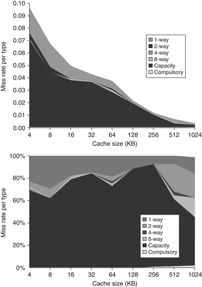
Figure B.9 Total miss rate (top) and distribution of miss rate (bottom) for each size cache according to the three C’s for the data in Figure B.8. The top diagram shows the actual data cache miss rates, while the bottom diagram shows the percentage in each category. (Space allows the graphs to show one extra cache size than can fit in Figure B.8.)
To show the benefit of associativity, conflict misses are divided into misses caused by each decrease in associativity. Here are the four divisions of conflict misses and how they are calculated:
As we can see from the figures, the compulsory miss rate of the SPEC2000 programs is very small, as it is for many long-running programs.
Having identified the three C’s, what can a computer designer do about them? Conceptually, conflicts are the easiest: Fully associative placement avoids all conflict misses. Full associativity is expensive in hardware, however, and may slow the processor clock rate (see the example on page B-29), leading to lower overall performance.
There is little to be done about capacity except to enlarge the cache. If the upper-level memory is much smaller than what is needed for a program, and a significant percentage of the time is spent moving data between two levels in the hierarchy, the memory hierarchy is said to thrash. Because so many replacements are required, thrashing means the computer runs close to the speed of the lower-level memory, or maybe even slower because of the miss overhead.
Another approach to improving the three C’s is to make blocks larger to reduce the number of compulsory misses, but, as we will see shortly, large blocks can increase other kinds of misses.
The three C’s give insight into the cause of misses, but this simple model has its limits; it gives you insight into average behavior but may not explain an individual miss. For example, changing cache size changes conflict misses as well as capacity misses, since a larger cache spreads out references to more blocks. Thus, a miss might move from a capacity miss to a conflict miss as cache size changes. Note that the three C’s also ignore replacement policy, since it is difficult to model and since, in general, it is less significant. In specific circumstances the replacement policy can actually lead to anomalous behavior, such as poorer miss rates for larger associativity, which contradicts the three C’s model. (Some have proposed using an address trace to determine optimal placement in memory to avoid placement misses from the three C’s model; we’ve not followed that advice here.)
Alas, many of the techniques that reduce miss rates also increase hit time or miss penalty. The desirability of reducing miss rates using the three optimizations must be balanced against the goal of making the whole system fast. This first example shows the importance of a balanced perspective.
First Optimization: Larger Block Size to Reduce Miss Rate
The simplest way to reduce miss rate is to increase the block size. Figure B.10 shows the trade-off of block size versus miss rate for a set of programs and cache sizes. Larger block sizes will reduce also compulsory misses. This reduction occurs because the principle of locality has two components: temporal locality and spatial locality. Larger blocks take advantage of spatial locality.

Figure B.10 Miss rate versus block size for five different-sized caches. Note that miss rate actually goes up if the block size is too large relative to the cache size. Each line represents a cache of different size. Figure B.11 shows the data used to plot these lines. Unfortunately, SPEC2000 traces would take too long if block size were included, so these data are based on SPEC92 on a DECstation 5000 [Gee et al. 1993].
At the same time, larger blocks increase the miss penalty. Since they reduce the number of blocks in the cache, larger blocks may increase conflict misses and even capacity misses if the cache is small. Clearly, there is little reason to increase the block size to such a size that it increases the miss rate. There is also no benefit to reducing miss rate if it increases the average memory access time. The increase in miss penalty may outweigh the decrease in miss rate.
Example
Figure B.11 shows the actual miss rates plotted in Figure B.10. Assume the memory system takes 80 clock cycles of overhead and then delivers 16 bytes every 2 clock cycles. Thus, it can supply 16 bytes in 82 clock cycles, 32 bytes in 84 clock cycles, and so on. Which block size has the smallest average memory access time for each cache size in Figure B.11?

Figure B.11 Actual miss rate versus block size for the five different-sized caches in Figure B.10. Note that for a 4 KB cache, 256-byte blocks have a higher miss rate than 32-byte blocks. In this example, the cache would have to be 256 KB in order for a 256-byte block to decrease misses.
Answer
If we assume the hit time is 1 clock cycle independent of block size, then the access time for a 16-byte block in a 4 KB cache is
and for a 256-byte block in a 256 KB cache the average memory access time is
Figure B.12 shows the average memory access time for all block and cache sizes between those two extremes. The boldfaced entries show the fastest block size for a given cache size: 32 bytes for 4 KB and 64 bytes for the larger caches. These sizes are, in fact, popular block sizes for processor caches today.

Figure B.12 Average memory access time versus block size for five different-sized caches in Figure B.10. Block sizes of 32 and 64 bytes dominate. The smallest average time per cache size is boldfaced.
As in all of these techniques, the cache designer is trying to minimize both the miss rate and the miss penalty. The selection of block size depends on both the latency and bandwidth of the lower-level memory. High latency and high bandwidth encourage large block size since the cache gets many more bytes per miss for a small increase in miss penalty. Conversely, low latency and low bandwidth encourage smaller block sizes since there is little time saved from a larger block. For example, twice the miss penalty of a small block may be close to the penalty of a block twice the size. The larger number of small blocks may also reduce conflict misses. Note that Figures B.10 and B.12 show the difference between selecting a block size based on minimizing miss rate versus minimizing average memory access time.
After seeing the positive and negative impact of larger block size on compulsory and capacity misses, the next two subsections look at the potential of higher capacity and higher associativity.
Second Optimization: Larger Caches to Reduce Miss Rate
The obvious way to reduce capacity misses in Figures B.8 and B.9 is to increase capacity of the cache. The obvious drawback is potentially longer hit time and higher cost and power. This technique has been especially popular in off-chip caches.
Third Optimization: Higher Associativity to Reduce Miss Rate
Figures B.8 and B.9 show how miss rates improve with higher associativity. There are two general rules of thumb that can be gleaned from these figures. The first is that eight-way set associative is for practical purposes as effective in reducing misses for these sized caches as fully associative. You can see the difference by comparing the eight-way entries to the capacity miss column in Figure B.8, since capacity misses are calculated using fully associative caches.
The second observation, called the 2:1 cache rule of thumb, is that a direct-mapped cache of size N has about the same miss rate as a two-way set associative cache of size N/2. This held in three C’s figures for cache sizes less than 128 KB.
Like many of these examples, improving one aspect of the average memory access time comes at the expense of another. Increasing block size reduces miss rate while increasing miss penalty, and greater associativity can come at the cost of increased hit time. Hence, the pressure of a fast processor clock cycle encourages simple cache designs, but the increasing miss penalty rewards associativity, as the following example suggests.
Example
Assume that higher associativity would increase the clock cycle time as listed below:

Assume that the hit time is 1 clock cycle, that the miss penalty for the direct-mapped case is 25 clock cycles to a level 2 cache (see next subsection) that never misses, and that the miss penalty need not be rounded to an integral number of clock cycles. Using Figure B.8 for miss rates, for which cache sizes are each of these three statements true?

Answer
Average memory access time for each associativity is

The miss penalty is the same time in each case, so we leave it as 25 clock cycles. For example, the average memory access time for a 4 KB direct-mapped cache is
and the time for a 512 KB, eight-way set associative cache is
Using these formulas and the miss rates from Figure B.8, Figure B.13 shows the average memory access time for each cache and associativity. The figure shows that the formulas in this example hold for caches less than or equal to 8 KB for up to four-way associativity. Starting with 16 KB, the greater hit time of larger associativity outweighs the time saved due to the reduction in misses.

Figure B.13 Average memory access time using miss rates in Figure B.8 for parameters in the example. Boldface type means that this time is higher than the number to the left, that is, higher associativity increases average memory access time.
Note that we did not account for the slower clock rate on the rest of the program in this example, thereby understating the advantage of direct-mapped cache.
Fourth Optimization: Multilevel Caches to Reduce Miss Penalty
Reducing cache misses had been the traditional focus of cache research, but the cache performance formula assures us that improvements in miss penalty can be just as beneficial as improvements in miss rate. Moreover, Figure 2.2 on page 74 shows that technology trends have improved the speed of processors faster than DRAMs, making the relative cost of miss penalties increase over time.
This performance gap between processors and memory leads the architect to this question: Should I make the cache faster to keep pace with the speed of processors, or make the cache larger to overcome the widening gap between the processor and main memory?
One answer is, do both. Adding another level of cache between the original cache and memory simplifies the decision. The first-level cache can be small enough to match the clock cycle time of the fast processor. Yet, the second-level cache can be large enough to capture many accesses that would go to main memory, thereby lessening the effective miss penalty.
Although the concept of adding another level in the hierarchy is straightforward, it complicates performance analysis. Definitions for a second level of cache are not always straightforward. Let’s start with the definition of average memory access time for a two-level cache. Using the subscripts L1 and L2 to refer, respectively, to a first-level and a second-level cache, the original formula is
and
so
In this formula, the second-level miss rate is measured on the leftovers from the first-level cache. To avoid ambiguity, these terms are adopted here for a two-level cache system:
This local miss rate is large for second-level caches because the first-level cache skims the cream of the memory accesses. This is why the global miss rate is the more useful measure: It indicates what fraction of the memory accesses that leave the processor go all the way to memory.
Here is a place where the misses per instruction metric shines. Instead of confusion about local or global miss rates, we just expand memory stalls per instruction to add the impact of a second-level cache.
Example
Suppose that in 1000 memory references there are 40 misses in the first-level cache and 20 misses in the second-level cache. What are the various miss rates? Assume the miss penalty from the L2 cache to memory is 200 clock cycles, the hit time of the L2 cache is 10 clock cycles, the hit time of L1 is 1 clock cycle, and there are 1.5 memory references per instruction. What is the average memory access time and average stall cycles per instruction? Ignore the impact of writes.
Answer
The miss rate (either local or global) for the first-level cache is 40/1000 or 4%. The local miss rate for the second-level cache is 20/40 or 50%. The global miss rate of the second-level cache is 20/1000 or 2%. Then
To see how many misses we get per instruction, we divide 1000 memory references by 1.5 memory references per instruction, which yields 667 instructions. Thus, we need to multiply the misses by 1.5 to get the number of misses per 1000 instructions. We have 40 × 1.5 or 60 L1 misses, and 20 × 1.5 or 30 L2 misses, per 1000 instructions. For average memory stalls per instruction, assuming the misses are distributed uniformly between instructions and data:

If we subtract the L1 hit time from the average memory access time (AMAT) and then multiply by the average number of memory references per instruction, we get the same average memory stalls per instruction:
As this example shows, there may be less confusion with multilevel caches when calculating using misses per instruction versus miss rates.
Note that these formulas are for combined reads and writes, assuming a write-back first-level cache. Obviously, a write-through first-level cache will send all writes to the second level, not just the misses, and a write buffer might be used.
Figures B.14 and B.15 show how miss rates and relative execution time change with the size of a second-level cache for one design. From these figures we can gain two insights. The first is that the global cache miss rate is very similar to the single cache miss rate of the second-level cache, provided that the second-level cache is much larger than the first-level cache. Hence, our intuition and knowledge about the first-level caches apply. The second insight is that the local cache miss rate is not a good measure of secondary caches; it is a function of the miss rate of the first-level cache, and hence can vary by changing the first-level cache. Thus, the global cache miss rate should be used when evaluating second-level caches.

Figure B.14 Miss rates versus cache size for multilevel caches. Second-level caches smaller than the sum of the two 64 KB first-level caches make little sense, as reflected in the high miss rates. After 256 KB the single cache is within 10% of the global miss rates. The miss rate of a single-level cache versus size is plotted against the local miss rate and global miss rate of a second-level cache using a 32 KB first-level cache. The L2 caches (unified) were two-way set associative with replacement. Each had split L1 instruction and data caches that were 64 KB two-way set associative with LRU replacement. The block size for both L1 and L2 caches was 64 bytes. Data were collected as in Figure B.4.
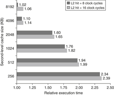
Figure B.15 Relative execution time by second-level cache size. The two bars are for different clock cycles for an L2 cache hit. The reference execution time of 1.00 is for an 8192 KB second-level cache with a 1-clock-cycle latency on a second-level hit. These data were collected the same way as in Figure B.14, using a simulator to imitate the Alpha 21264.
With these definitions in place, we can consider the parameters of second-level caches. The foremost difference between the two levels is that the speed of the first-level cache affects the clock rate of the processor, while the speed of the second-level cache only affects the miss penalty of the first-level cache. Thus, we can consider many alternatives in the second-level cache that would be ill chosen for the first-level cache. There are two major questions for the design of the second-level cache: Will it lower the average memory access time portion of the CPI, and how much does it cost?
The initial decision is the size of a second-level cache. Since everything in the first-level cache is likely to be in the second-level cache, the second-level cache should be much bigger than the first. If second-level caches are just a little bigger, the local miss rate will be high. This observation inspires the design of huge second-level caches—the size of main memory in older computers!
One question is whether set associativity makes more sense for second-level caches.
Example
Given the data below, what is the impact of second-level cache associativity on its miss penalty?
Answer
For a direct-mapped second-level cache, the first-level cache miss penalty is
Adding the cost of associativity increases the hit cost only 0.1 clock cycle, making the new first-level cache miss penalty:
In reality, second-level caches are almost always synchronized with the first-level cache and processor. Accordingly, the second-level hit time must be an integral number of clock cycles. If we are lucky, we shave the second-level hit time to 10 cycles; if not, we round up to 11 cycles. Either choice is an improvement over the direct-mapped second-level cache:

Now we can reduce the miss penalty by reducing the miss rate of the second-level caches.
Another consideration concerns whether data in the first-level cache are in the second-level cache. Multilevel inclusion is the natural policy for memory hierarchies: L1 data are always present in L2. Inclusion is desirable because consistency between I/O and caches (or among caches in a multiprocessor) can be determined just by checking the second-level cache.
One drawback to inclusion is that measurements can suggest smaller blocks for the smaller first-level cache and larger blocks for the larger second-level cache. For example, the Pentium 4 has 64-byte blocks in its L1 caches and 128-byte blocks in its L2 cache. Inclusion can still be maintained with more work on a second-level miss. The second-level cache must invalidate all first-level blocks that map onto the second-level block to be replaced, causing a slightly higher first-level miss rate. To avoid such problems, many cache designers keep the block size the same in all levels of caches.
However, what if the designer can only afford an L2 cache that is slightly bigger than the L1 cache? Should a significant portion of its space be used as a redundant copy of the L1 cache? In such cases a sensible opposite policy is multilevel exclusion: L1 data are never found in an L2 cache. Typically, with exclusion a cache miss in L1 results in a swap of blocks between L1 and L2 instead of a replacement of an L1 block with an L2 block. This policy prevents wasting space in the L2 cache. For example, the AMD Opteron chip obeys the exclusion property using two 64 KB L1 caches and 1 MB L2 cache.
As these issues illustrate, although a novice might design the first- and second-level caches independently, the designer of the first-level cache has a simpler job given a compatible second-level cache. It is less of a gamble to use a write-through, for example, if there is a write-back cache at the next level to act as a backstop for repeated writes and it uses multilevel inclusion.
The essence of all cache designs is balancing fast hits and few misses. For second-level caches, there are many fewer hits than in the first-level cache, so the emphasis shifts to fewer misses. This insight leads to much larger caches and techniques to lower the miss rate, such as higher associativity and larger blocks.
Fifth Optimization: Giving Priority to Read Misses over Writes to Reduce Miss Penalty
This optimization serves reads before writes have been completed. We start with looking at the complexities of a write buffer.
With a write-through cache the most important improvement is a write buffer of the proper size. Write buffers, however, do complicate memory accesses because they might hold the updated value of a location needed on a read miss.
Example

Assume a direct-mapped, write-through cache that maps 512 and 1024 to the same block, and a four-word write buffer that is not checked on a read miss. Will the value in R2 always be equal to the value in R3?
Answer
Using the terminology from Chapter 2, this is a read-after-write data hazard in memory. Let’s follow a cache access to see the danger. The data in R3 are placed into the write buffer after the store. The following load uses the same cache index and is therefore a miss. The second load instruction tries to put the value in location 512 into register R2; this also results in a miss. If the write buffer hasn’t completed writing to location 512 in memory, the read of location 512 will put the old, wrong value into the cache block, and then into R2. Without proper precautions, R3 would not be equal to R2!
The simplest way out of this dilemma is for the read miss to wait until the write buffer is empty. The alternative is to check the contents of the write buffer on a read miss, and if there are no conflicts and the memory system is available, let the read miss continue. Virtually all desktop and server processors use the latter approach, giving reads priority over writes.
The cost of writes by the processor in a write-back cache can also be reduced. Suppose a read miss will replace a dirty memory block. Instead of writing the dirty block to memory, and then reading memory, we could copy the dirty block to a buffer, then read memory, and then write memory. This way the processor read, for which the processor is probably waiting, will finish sooner. Similar to the previous situation, if a read miss occurs, the processor can either stall until the buffer is empty or check the addresses of the words in the buffer for conflicts.
Now that we have five optimizations that reduce cache miss penalties or miss rates, it is time to look at reducing the final component of average memory access time. Hit time is critical because it can affect the clock rate of the processor; in many processors today the cache access time limits the clock cycle rate, even for processors that take multiple clock cycles to access the cache. Hence, a fast hit time is multiplied in importance beyond the average memory access time formula because it helps everything.
Sixth Optimization: Avoiding Address Translation during Indexing of the Cache to Reduce Hit Time
Even a small and simple cache must cope with the translation of a virtual address from the processor to a physical address to access memory. As described in Section B.4, processors treat main memory as just another level of the memory hierarchy, and thus the address of the virtual memory that exists on disk must be mapped onto the main memory.
The guideline of making the common case fast suggests that we use virtual addresses for the cache, since hits are much more common than misses. Such caches are termed virtual caches, with physical cache used to identify the traditional cache that uses physical addresses. As we will shortly see, it is important to distinguish two tasks: indexing the cache and comparing addresses. Thus, the issues are whether a virtual or physical address is used to index the cache and whether a virtual or physical address is used in the tag comparison. Full virtual addressing for both indices and tags eliminates address translation time from a cache hit. Then why doesn’t everyone build virtually addressed caches?
One reason is protection. Page-level protection is checked as part of the virtual to physical address translation, and it must be enforced no matter what. One solution is to copy the protection information from the TLB on a miss, add a field to hold it, and check it on every access to the virtually addressed cache.
Another reason is that every time a process is switched, the virtual addresses refer to different physical addresses, requiring the cache to be flushed. Figure B.16 shows the impact on miss rates of this flushing. One solution is to increase the width of the cache address tag with a process-identifier tag (PID). If the operating system assigns these tags to processes, it only need flush the cache when a PID is recycled; that is, the PID distinguishes whether or not the data in the cache are for this program. Figure B.16 shows the improvement in miss rates by using PIDs to avoid cache flushes.

Figure B.16 Miss rate versus virtually addressed cache size of a program measured three ways: without process switches (uniprocess), with process switches using a process-identifier tag (PID), and with process switches but without PIDs (purge). PIDs increase the uniprocess absolute miss rate by 0.3% to 0.6% and save 0.6% to 4.3% over purging. Agarwal [1987] collected these statistics for the Ultrix operating system running on a VAX, assuming direct-mapped caches with a block size of 16 bytes. Note that the miss rate goes up from 128K to 256K. Such nonintuitive behavior can occur in caches because changing size changes the mapping of memory blocks onto cache blocks, which can change the conflict miss rate.
A third reason why virtual caches are not more popular is that operating systems and user programs may use two different virtual addresses for the same physical address. These duplicate addresses, called synonyms or aliases, could result in two copies of the same data in a virtual cache; if one is modified, the other will have the wrong value. With a physical cache this wouldn’t happen, since the accesses would first be translated to the same physical cache block.
Hardware solutions to the synonym problem, called antialiasing, guarantee every cache block a unique physical address. For example, the AMD Opteron uses a 64 KB instruction cache with a 4 KB page and two-way set associativity; hence, the hardware must handle aliases involved with the three virtual address bits in the set index. It avoids aliases by simply checking all eight possible locations on a miss—two blocks in each of four sets—to be sure that none matches the physical address of the data being fetched. If one is found, it is invalidated, so when the new data are loaded into the cache their physical address is guaranteed to be unique.
Software can make this problem much easier by forcing aliases to share some address bits. An older version of UNIX from Sun Microsystems, for example, required all aliases to be identical in the last 18 bits of their addresses; this restriction is called page coloring. Note that page coloring is simply set associative mapping applied to virtual memory: The 4 KB (212) pages are mapped using 64 (26) sets to ensure that the physical and virtual addresses match in the last 18 bits. This restriction means a direct-mapped cache that is 218 (256K) bytes or smaller can never have duplicate physical addresses for blocks. From the perspective of the cache, page coloring effectively increases the page offset, as software guarantees that the last few bits of the virtual and physical page address are identical.
The final area of concern with virtual addresses is I/O. I/O typically uses physical addresses and thus would require mapping to virtual addresses to interact with a virtual cache. (The impact of I/O on caches is further discussed in Appendix D.)
One alternative to get the best of both virtual and physical caches is to use part of the page offset—the part that is identical in both virtual and physical addresses—to index the cache. At the same time as the cache is being read using that index, the virtual part of the address is translated, and the tag match uses physical addresses.
This alternative allows the cache read to begin immediately, and yet the tag comparison is still with physical addresses. The limitation of this virtually indexed, physically tagged alternative is that a direct-mapped cache can be no bigger than the page size. For example, in the data cache in Figure B.5 on page B-13, the index is 9 bits and the cache block offset is 6 bits. To use this trick, the virtual page size would have to be at least 2(9+6) bytes or 32 KB. If not, a portion of the index must be translated from virtual to physical address. Figure B.17 shows the organization of the caches, translation lookaside buffers (TLBs), and virtual memory when this technique is used.

Figure B.17 The overall picture of a hypothetical memory hierarchy going from virtual address to L2 cache access. The page size is 16 KB. The TLB is two-way set associative with 256 entries. The L1 cache is a direct-mapped 16 KB, and the L2 cache is a four-way set associative with a total of 4 MB. Both use 64-byte blocks. The virtual address is 64 bits and the physical address is 40 bits.
Associativity can keep the index in the physical part of the address and yet still support a large cache. Recall that the size of the index is controlled by this formula:
For example, doubling associativity and doubling the cache size does not change the size of the index. The IBM 3033 cache, as an extreme example, is 16-way set associative, even though studies show there is little benefit to miss rates above 8-way set associativity. This high associativity allows a 64 KB cache to be addressed with a physical index, despite the handicap of 4 KB pages in the IBM architecture.
Summary of Basic Cache Optimization
The techniques in this section to improve miss rate, miss penalty, and hit time generally impact the other components of the average memory access equation as well as the complexity of the memory hierarchy. Figure B.18 summarizes these techniques and estimates the impact on complexity, with + meaning that the technique improves the factor, – meaning it hurts that factor, and blank meaning it has no impact. No optimization in this figure helps more than one category.
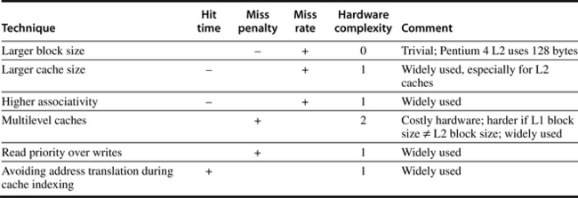
Figure B.18 Summary of basic cache optimizations showing impact on cache performance and complexity for the techniques in this appendix. Generally a technique helps only one factor. + means that the technique improves the factor, – means it hurts that factor, and blank means it has no impact. The complexity measure is subjective, with 0 being the easiest and 3 being a challenge.
B.4 Virtual Memory
… a system has been devised to make the core drum combination appear to the programmer as a single level store, the requisite transfers taking place automatically.
At any instant in time computers are running multiple processes, each with its own address space. (Processes are described in the next section.) It would be too expensive to dedicate a full address space worth of memory for each process, especially since many processes use only a small part of their address space. Hence, there must be a means of sharing a smaller amount of physical memory among many processes.
One way to do this, virtual memory, divides physical memory into blocks and allocates them to different processes. Inherent in such an approach must be a protection scheme that restricts a process to the blocks belonging only to that process. Most forms of virtual memory also reduce the time to start a program, since not all code and data need be in physical memory before a program can begin.
Although protection provided by virtual memory is essential for current computers, sharing is not the reason that virtual memory was invented. If a program became too large for physical memory, it was the programmer’s job to make it fit. Programmers divided programs into pieces, then identified the pieces that were mutually exclusive, and loaded or unloaded these overlays under user program control during execution. The programmer ensured that the program never tried to access more physical main memory than was in the computer, and that the proper overlay was loaded at the proper time. As you can well imagine, this responsibility eroded programmer productivity.
Virtual memory was invented to relieve programmers of this burden; it automatically manages the two levels of the memory hierarchy represented by main memory and secondary storage. Figure B.19 shows the mapping of virtual memory to physical memory for a program with four pages.

Figure B.19 The logical program in its contiguous virtual address space is shown on the left. It consists of four pages, A, B, C, and D. The actual location of three of the blocks is in physical main memory and the other is located on the disk.
In addition to sharing protected memory space and automatically managing the memory hierarchy, virtual memory also simplifies loading the program for execution. Called relocation, this mechanism allows the same program to run in any location in physical memory. The program in Figure B.19 can be placed anywhere in physical memory or disk just by changing the mapping between them. (Prior to the popularity of virtual memory, processors would include a relocation register just for that purpose.) An alternative to a hardware solution would be software that changed all addresses in a program each time it was run.
Several general memory hierarchy ideas from Chapter 1 about caches are analogous to virtual memory, although many of the terms are different. Page or segment is used for block, and page fault or address fault is used for miss. With virtual memory, the processor produces virtual addresses that are translated by a combination of hardware and software to physical addresses, which access main memory. This process is called memory mapping or address translation. Today, the two memory hierarchy levels controlled by virtual memory are DRAMs and magnetic disks. Figure B.20 shows a typical range of memory hierarchy parameters for virtual memory.

Figure B.20 Typical ranges of parameters for caches and virtual memory. Virtual memory parameters represent increases of 10 to 1,000,000 times over cache para-meters. Normally, first-level caches contain at most 1 MB of data, whereas physical memory contains 256 MB to 1 TB.
There are further differences between caches and virtual memory beyond those quantitative ones mentioned in Figure B.20:
Virtual memory also encompasses several related techniques. Virtual memory systems can be categorized into two classes: those with fixed-size blocks, called pages, and those with variable-size blocks, called segments. Pages are typically fixed at 4096 to 8192 bytes, while segment size varies. The largest segment supported on any processor ranges from 216 bytes up to 232 bytes; the smallest segment is 1 byte. Figure B.21 shows how the two approaches might divide code and data.

The decision to use paged virtual memory versus segmented virtual memory affects the processor. Paged addressing has a single fixed-size address divided into page number and offset within a page, analogous to cache addressing. A single address does not work for segmented addresses; the variable size of segments requires 1 word for a segment number and 1 word for an offset within a segment, for a total of 2 words. An unsegmented address space is simpler for the compiler.
The pros and cons of these two approaches have been well documented in operating systems textbooks; Figure B.22 summarizes the arguments. Because of the replacement problem (the third line of the figure), few computers today use pure segmentation. Some computers use a hybrid approach, called paged segments, in which a segment is an integral number of pages. This simplifies replacement because memory need not be contiguous, and the full segments need not be in main memory. A more recent hybrid is for a computer to offer multiple page sizes, with the larger sizes being powers of 2 times the smallest page size. The IBM 405CR embedded processor, for example, allows 1 KB, 4 KB (22 × 1 KB), 16 KB (24 × 1 KB), 64 KB (26 × 1 KB), 256 KB (28 × 1 KB), 1024 KB (210 × 1 KB), and 4096 KB (212× 1 KB) to act as a single page.

Figure B.22 Paging versus segmentation. Both can waste memory, depending on the block size and how well the segments fit together in main memory. Programming languages with unrestricted pointers require both the segment and the address to be passed. A hybrid approach, called paged segments, shoots for the best of both worlds: Segments are composed of pages, so replacing a block is easy, yet a segment may be treated as a logical unit.
Four Memory Hierarchy Questions Revisited
We are now ready to answer the four memory hierarchy questions for virtual memory.
Q1: Where Can a Block Be Placed in Main Memory?
The miss penalty for virtual memory involves access to a rotating magnetic storage device and is therefore quite high. Given the choice of lower miss rates or a simpler placement algorithm, operating systems designers normally pick lower miss rates because of the exorbitant miss penalty. Thus, operating systems allow blocks to be placed anywhere in main memory. According to the terminology in Figure B.2 on page B-8, this strategy would be labeled fully associative.
Q2: How Is a Block Found If It Is in Main Memory?
Both paging and segmentation rely on a data structure that is indexed by the page or segment number. This data structure contains the physical address of the block. For segmentation, the offset is added to the segment’s physical address to obtain the final physical address. For paging, the offset is simply concatenated to this physical page address (see Figure B.23).

This data structure, containing the physical page addresses, usually takes the form of a page table. Indexed by the virtual page number, the size of the table is the number of pages in the virtual address space. Given a 32-bit virtual address, 4 KB pages, and 4 bytes per page table entry (PTE), the size of the page table would be (232/212) × 22 = 222 or 4 MB.
To reduce the size of this data structure, some computers apply a hashing function to the virtual address. The hash allows the data structure to be the length of the number of physical pages in main memory. This number could be much smaller than the number of virtual pages. Such a structure is called an inverted page table. Using the previous example, a 512 MB physical memory would only need 1 MB (8 × 512 MB/4 KB) for an inverted page table; the extra 4 bytes per page table entry are for the virtual address. The HP/Intel IA-64 covers both bases by offering both traditional pages tables and inverted page tables, leaving the choice of mechanism to the operating system programmer.
To reduce address translation time, computers use a cache dedicated to these address translations, called a translation lookaside buffer, or simply translation buffer, described in more detail shortly.
Q3: Which Block Should Be Replaced on a Virtual Memory Miss?
As mentioned earlier, the overriding operating system guideline is minimizing page faults. Consistent with this guideline, almost all operating systems try to replace the least recently used (LRU) block because if the past predicts the future, that is the one less likely to be needed.
To help the operating system estimate LRU, many processors provide a use bit or reference bit, which is logically set whenever a page is accessed. (To reduce work, it is actually set only on a translation buffer miss, which is described shortly.) The operating system periodically clears the use bits and later records them so it can determine which pages were touched during a particular time period. By keeping track in this way, the operating system can select a page that is among the least recently referenced.
Q4: What Happens on a Write?
The level below main memory contains rotating magnetic disks that take millions of clock cycles to access. Because of the great discrepancy in access time, no one has yet built a virtual memory operating system that writes through main memory to disk on every store by the processor. (This remark should not be interpreted as an opportunity to become famous by being the first to build one!) Thus, the write strategy is always write-back.
Since the cost of an unnecessary access to the next-lower level is so high, virtual memory systems usually include a dirty bit. It allows blocks to be written to disk only if they have been altered since being read from the disk.
Techniques for Fast Address Translation
Page tables are usually so large that they are stored in main memory and are sometimes paged themselves. Paging means that every memory access logically takes at least twice as long, with one memory access to obtain the physical address and a second access to get the data. As mentioned in Chapter 2, we use locality to avoid the extra memory access. By keeping address translations in a special cache, a memory access rarely requires a second access to translate the data. This special address translation cache is referred to as a translation look aside buffer (TLB), also called a translation buffer (TB).
A TLB entry is like a cache entry where the tag holds portions of the virtual address and the data portion holds a physical page frame number, protection field, valid bit, and usually a use bit and dirty bit. To change the physical page frame number or protection of an entry in the page table, the operating system must make sure the old entry is not in the TLB; otherwise, the system won’t behave properly. Note that this dirty bit means the corresponding page is dirty, not that the address translation in the TLB is dirty nor that a particular block in the data cache is dirty. The operating system resets these bits by changing the value in the page table and then invalidates the corresponding TLB entry. When the entry is reloaded from the page table, the TLB gets an accurate copy of the bits.
Figure B.24 shows the Opteron data TLB organization, with each step of the translation labeled. This TLB uses fully associative placement; thus, the translation begins (steps 1 and 2) by sending the virtual address to all tags. Of course, the tag must be marked valid to allow a match. At the same time, the type of memory access is checked for a violation (also in step 2) against protection information in the TLB.

Figure B.24 Operation of the Opteron data TLB during address translation. The four steps of a TLB hit are shown as circled numbers. This TLB has 40 entries. Section B.5 describes the various protection and access fields of an Opteron page table entry.
For reasons similar to those in the cache case, there is no need to include the 12 bits of the page offset in the TLB. The matching tag sends the corresponding physical address through effectively a 40:1 multiplexor (step 3). The page offset is then combined with the physical page frame to form a full physical address (step 4). The address size is 40 bits.
Address translation can easily be on the critical path determining the clock cycle of the processor, so the Opteron uses virtually addressed, physically tagged L1 caches.
Selecting a Page Size
The most obvious architectural parameter is the page size. Choosing the page is a question of balancing forces that favor a larger page size versus those favoring a smaller size. The following favor a larger size:
It is for this final reason that recent microprocessors have decided to support multiple page sizes; for some programs, TLB misses can be as significant on CPI as the cache misses.
The main motivation for a smaller page size is conserving storage. A small page size will result in less wasted storage when a contiguous region of virtual memory is not equal in size to a multiple of the page size. The term for this unused memory in a page is internal fragmentation. Assuming that each process has three primary segments (text, heap, and stack), the average wasted storage per process will be 1.5 times the page size. This amount is negligible for computers with hundreds of megabytes of memory and page sizes of 4 KB to 8 KB. Of course, when the page sizes become very large (more than 32 KB), storage (both main and secondary) could be wasted, as well as I/O bandwidth. A final concern is process start-up time; many processes are small, so a large page size would lengthen the time to invoke a process.
Summary of Virtual Memory and Caches
With virtual memory, TLBs, first-level caches, and second-level caches all mapping portions of the virtual and physical address space, it can get confusing what bits go where. Figure B.25 gives a hypothetical example going from a 64-bit virtual address to a 41-bit physical address with two levels of cache. This L1 cache is virtually indexed, physically tagged since both the cache size and the page size are 8 KB. The L2 cache is 4 MB. The block size for both is 64 bytes.

Figure B.25 The overall picture of a hypothetical memory hierarchy going from virtual address to L2 cache access. The page size is 8 KB. The TLB is direct mapped with 256 entries. The L1 cache is a direct-mapped 8 KB, and the L2 cache is a direct-mapped 4 MB. Both use 64-byte blocks. The virtual address is 64 bits and the physical address is 41 bits. The primary difference between this simple figure and a real cache is replication of pieces of this figure.
First, the 64-bit virtual address is logically divided into a virtual page number and page offset. The former is sent to the TLB to be translated into a physical address, and the high bit of the latter is sent to the L1 cache to act as an index. If the TLB match is a hit, then the physical page number is sent to the L1 cache tag to check for a match. If it matches, it’s an L1 cache hit. The block offset then selects the word for the processor.
If the L1 cache check results in a miss, the physical address is then used to try the L2 cache. The middle portion of the physical address is used as an index to the 4 MB L2 cache. The resulting L2 cache tag is compared to the upper part of the physical address to check for a match. If it matches, we have an L2 cache hit, and the data are sent to the processor, which uses the block offset to select the desired word. On an L2 miss, the physical address is then used to get the block from memory.
Although this is a simple example, the major difference between this drawing and a real cache is replication. First, there is only one L1 cache. When there are two L1 caches, the top half of the diagram is duplicated. Note that this would lead to two TLBs, which is typical. Hence, one cache and TLB is for instructions, driven from the PC, and one cache and TLB is for data, driven from the effective address.
The second simplification is that all the caches and TLBs are direct mapped. If any were n -way set associative, then we would replicate each set of tag memory, comparators, and data memory n times and connect data memories with an n:1 multiplexor to select a hit. Of course, if the total cache size remained the same, the cache index would also shrink by log2n bits according to the formula in Figure B.7 on page B-22.
B.5 Protection and Examples of Virtual Memory
The invention of multiprogramming, where a computer would be shared by several programs running concurrently, led to new demands for protection and sharing among programs. These demands are closely tied to virtual memory in computers today, and so we cover the topic here along with two examples of virtual memory.
Multiprogramming leads to the concept of a process. Metaphorically, a process is a program’s breathing air and living space—that is, a running program plus any state needed to continue running it. Time-sharing is a variation of multiprogramming that shares the processor and memory with several interactive users at the same time, giving the illusion that all users have their own computers. Thus, at any instant it must be possible to switch from one process to another. This exchange is called a process switch or context switch.
A process must operate correctly whether it executes continuously from start to finish, or it is interrupted repeatedly and switched with other processes. The responsibility for maintaining correct process behavior is shared by designers of the computer and the operating system. The computer designer must ensure that the processor portion of the process state can be saved and restored. The operating system designer must guarantee that processes do not interfere with each others’ computations.
The safest way to protect the state of one process from another would be to copy the current information to disk. However, a process switch would then take seconds—far too long for a time-sharing environment.
This problem is solved by operating systems partitioning main memory so that several different processes have their state in memory at the same time. This division means that the operating system designer needs help from the computer designer to provide protection so that one process cannot modify another. Besides protection, the computers also provide for sharing of code and data between processes, to allow communication between processes or to save memory by reducing the number of copies of identical information.
Protecting Processes
Processes can be protected from one another by having their own page tables, each pointing to distinct pages of memory. Obviously, user programs must be prevented from modifying their page tables or protection would be circumvented.
Protection can be escalated, depending on the apprehension of the computer designer or the purchaser. Rings added to the processor protection structure expand memory access protection from two levels (user and kernel) to many more. Like a military classification system of top secret, secret, confidential, and unclassified, concentric rings of security levels allow the most trusted to access anything, the second most trusted to access everything except the innermost level, and so on. The “civilian” programs are the least trusted and, hence, have the most limited range of accesses. There may also be restrictions on what pieces of memory can contain code—execute protection—and even on the entrance point between the levels. The Intel 80×86 protection structure, which uses rings, is described later in this section. It is not clear whether rings are an improvement in practice over the simple system of user and kernel modes.
As the designer’s apprehension escalates to trepidation, these simple rings may not suffice. Restricting the freedom given a program in the inner sanctum requires a new classification system. Instead of a military model, the analogy of this system is to keys and locks: A program can’t unlock access to the data unless it has the key. For these keys, or capabilities, to be useful, the hardware and operating system must be able to explicitly pass them from one program to another without allowing a program itself to forge them. Such checking requires a great deal of hardware support if time for checking keys is to be kept low.
The 80×86 architecture has tried several of these alternatives over the years. Since backwards compatibility is one of the guidelines of this architecture, the most recent versions of the architecture include all of its experiments in virtual memory. We’ll go over two of the options here: first the older segmented address space and then the newer flat, 64-bit address space.
A Segmented Virtual Memory Example: Protection in the Intel Pentium
The second system is the most dangerous system a man ever designs. … The general tendency is to over-design the second system, using all the ideas and frills that were cautiously sidetracked on the first one.
The original 8086 used segments for addressing, yet it provided nothing for virtual memory or for protection. Segments had base registers but no bound registers and no access checks, and before a segment register could be loaded the corresponding segment had to be in physical memory. Intel’s dedication to virtual memory and protection is evident in the successors to the 8086, with a few fields extended to support larger addresses. This protection scheme is elaborate, with many details carefully designed to try to avoid security loopholes. We’ll refer to it as IA-32. The next few pages highlight a few of the Intel safeguards; if you find the reading difficult, imagine the difficulty of implementing them!
The first enhancement is to double the traditional two-level protection model: The IA-32 has four levels of protection. The innermost level (0) corresponds to the traditional kernel mode, and the outermost level (3) is the least privileged mode. The IA-32 has separate stacks for each level to avoid security breaches between the levels. There are also data structures analogous to traditional page tables that contain the physical addresses for segments, as well as a list of checks to be made on translated addresses.
The Intel designers did not stop there. The IA-32 divides the address space, allowing both the operating system and the user access to the full space. The IA-32 user can call an operating system routine in this space and even pass parameters to it while retaining full protection. This safe call is not a trivial action, since the stack for the operating system is different from the user’s stack. Moreover, the IA-32 allows the operating system to maintain the protection level of the called routine for the parameters that are passed to it. This potential loophole in protection is prevented by not allowing the user process to ask the operating system to access something indirectly that it would not have been able to access itself. (Such security loopholes are called Trojan horses.)
The Intel designers were guided by the principle of trusting the operating system as little as possible, while supporting sharing and protection. As an example of the use of such protected sharing, suppose a payroll program writes checks and also updates the year-to-date information on total salary and benefits payments. Thus, we want to give the program the ability to read the salary and year-to-date information and modify the year-to-date information but not the salary. We will see the mechanism to support such features shortly. In the rest of this subsection, we will look at the big picture of the IA-32 protection and examine its motivation.
Adding Bounds Checking and Memory Mapping
The first step in enhancing the Intel processor was getting the segmented addressing to check bounds as well as supply a base. Rather than a base address, the segment registers in the IA-32 contain an index to a virtual memory data structure called a descriptor table. Descriptor tables play the role of traditional page tables. On the IA-32 the equivalent of a page table entry is a segment descriptor. It contains fields found in PTEs:
There is also a limit field, not found in paged systems, which establishes the upper bound of valid offsets for this segment. Figure B.26 shows examples of IA-32 segment descriptors.

Figure B.26 The IA-32 segment descriptors are distinguished by bits in the attributes field. Base, limit, present, readable, and writable are all self-explanatory. D gives the default addressing size of the instructions: 16 bits or 32 bits. G gives the granularity of the segment limit: 0 means in bytes and 1 means in 4 KB pages. G is set to 1 when paging is turned on to set the size of the page tables. DPL means descriptor privilege level—this is checked against the code privilege level to see if the access will be allowed. Conforming says the code takes on the privilege level of the code being called rather than the privilege level of the caller; it is used for library routines. The expand-down field flips the check to let the base field be the high-water mark and the limit field be the low-water mark. As you might expect, this is used for stack segments that grow down. Word count controls the number of words copied from the current stack to the new stack on a call gate. The other two fields of the call gate descriptor, destination selector and destination offset, select the descriptor of the destination of the call and the offset into it, respectively. There are many more than these three segment descriptors in the IA-32 protection model.
IA-32 provides an optional paging system in addition to this segmented addressing. The upper portion of the 32-bit address selects the segment descriptor, and the middle portion is an index into the page table selected by the descriptor. We describe below the protection system that does not rely on paging.
Adding Sharing and Protection
To provide for protected sharing, half of the address space is shared by all processes and half is unique to each process, called global address space and local address space, respectively. Each half is given a descriptor table with the appropriate name. A descriptor pointing to a shared segment is placed in the global descriptor table, while a descriptor for a private segment is placed in the local descriptor table.
A program loads an IA-32 segment register with an index to the table and a bit saying which table it desires. The operation is checked according to the attributes in the descriptor, the physical address being formed by adding the offset in the processor to the base in the descriptor, provided the offset is less than the limit field. Every segment descriptor has a separate 2-bit field to give the legal access level of this segment. A violation occurs only if the program tries to use a segment with a lower protection level in the segment descriptor.
We can now show how to invoke the payroll program mentioned above to update the year-to-date information without allowing it to update salaries. The program could be given a descriptor to the information that has the writable field clear, meaning it can read but not write the data. A trusted program can then be supplied that will only write the year-to-date information. It is given a descriptor with the writable field set (Figure B.26). The payroll program invokes the trusted code using a code segment descriptor with the conforming field set. This setting means the called program takes on the privilege level of the code being called rather than the privilege level of the caller. Hence, the payroll program can read the salaries and call a trusted program to update the year-to-date totals, yet the payroll program cannot modify the salaries. If a Trojan horse exists in this system, to be effective it must be located in the trusted code whose only job is to update the year-to-date information. The argument for this style of protection is that limiting the scope of the vulnerability enhances security.
Adding Safe Calls from User to OS Gates and Inheriting Protection Level for Parameters
Allowing the user to jump into the operating system is a bold step. How, then, can a hardware designer increase the chances of a safe system without trusting the operating system or any other piece of code? The IA-32 approach is to restrict where the user can enter a piece of code, to safely place parameters on the proper stack, and to make sure the user parameters don’t get the protection level of the called code.
To restrict entry into others’ code, the IA-32 provides a special segment descriptor, or call gate, identified by a bit in the attributes field. Unlike other descriptors, call gates are full physical addresses of an object in memory; the offset supplied by the processor is ignored. As stated above, their purpose is to prevent the user from randomly jumping anywhere into a protected or more privileged code segment. In our programming example, this means the only place the payroll program can invoke the trusted code is at the proper boundary. This restriction is needed to make conforming segments work as intended.
What happens if caller and callee are “mutually suspicious,” so that neither trusts the other? The solution is found in the word count field in the bottom descriptor in Figure B.26. When a call instruction invokes a call gate descriptor, the descriptor copies the number of words specified in the descriptor from the local stack onto the stack corresponding to the level of this segment. This copying allows the user to pass parameters by first pushing them onto the local stack. The hardware then safely transfers them onto the correct stack. A return from a call gate will pop the parameters off both stacks and copy any return values to the proper stack. Note that this model is incompatible with the current practice of passing parameters in registers.
This scheme still leaves open the potential loophole of having the operating system use the user’s address, passed as parameters, with the operating system’s security level, instead of with the user’s level. The IA-32 solves this problem by dedicating 2 bits in every processor segment register to the requested protection level. When an operating system routine is invoked, it can execute an instruction that sets this 2-bit field in all address parameters with the protection level of the user that called the routine. Thus, when these address parameters are loaded into the segment registers, they will set the requested protection level to the proper value. The IA-32 hardware then uses the requested protection level to prevent any foolishness: No segment can be accessed from the system routine using those parameters if it has a more privileged protection level than requested.
A Paged Virtual Memory Example: The 64-Bit Opteron Memory Management
AMD engineers found few uses of the elaborate protection model described above. The popular model is a flat, 32-bit address space, introduced by the 80386, which sets all the base values of the segment registers to zero. Hence, AMD dispensed with the multiple segments in the 64-bit mode. It assumes that the segment base is zero and ignores the limit field. The page sizes are 4 KB, 2 MB, and 4 MB.
The 64-bit virtual address of the AMD64 architecture is mapped onto 52-bit physical addresses, although implementations can implement fewer bits to simplify hardware. The Opteron, for example, uses 48-bit virtual addresses and 40-bit physical addresses. AMD64 requires that the upper 16 bits of the virtual address be just the sign extension of the lower 48 bits, which it calls canonical form.
The size of page tables for the 64-bit address space is alarming. Hence, AMD64 uses a multilevel hierarchical page table to map the address space to keep the size reasonable. The number of levels depends on the size of the virtual address space. Figure B.27 shows the four-level translation of the 48-bit virtual addresses of the Opteron.

Figure B.27 The mapping of an Opteron virtual address. The Opteron virtual memory implementation with four page table levels supports an effective physical address size of 40 bits. Each page table has 512 entries, so each level field is 9 bits wide. The AMD64 architecture document allows the virtual address size to grow from the current 48 bits to 64 bits, and the physical address size to grow from the current 40 bits to 52 bits.
The offsets for each of these page tables come from four 9-bit fields. Address translation starts with adding the first offset to the page-map level 4 base register and then reading memory from this location to get the base of the next-level page table. The next address offset is in turn added to this newly fetched address, and memory is accessed again to determine the base of the third page table. It happens again in the same fashion. The last address field is added to this final base address, and memory is read using this sum to (finally) get the physical address of the page being referenced. This address is concatenated with the 12-bit page offset to get the full physical address. Note that the page table in the Opteron architecture fits within a single 4 KB page.
The Opteron uses a 64-bit entry in each of these page tables. The first 12 bits are reserved for future use, the next 52 bits contain the physical page frame number, and the last 12 bits give the protection and use information. Although the fields vary some between the page table levels, here are the basic ones:
Since the Opteron normally goes through four levels of tables on a TLB miss, there are three potential places to check protection restrictions. The Opteron obeys only the bottom-level PTE, checking the others only to be sure the valid bit is set.
As the entry is 8 bytes long, each page table has 512 entries, and the Opteron has 4 KB pages, the page tables are exactly one page long. Each of the four level fields are 9 bits long, and the page offset is 12 bits. This derivation leaves 64 − (4 × 9 + 12) or 16 bits to be sign extended to ensure canonical addresses.
Although we have explained translation of legal addresses, what prevents the user from creating illegal address translations and getting into mischief? The page tables themselves are protected from being written by user programs. Thus, the user can try any virtual address, but by controlling the page table entries the operating system controls what physical memory is accessed. Sharing of memory between processes is accomplished by having a page table entry in each address space point to the same physical memory page.
The Opteron employs four TLBs to reduce address translation time, two for instruction accesses and two for data accesses. Like multilevel caches, the Opteron reduces TLB misses by having two larger L2 TLBs: one for instructions and one for data. Figure B.28 describes the data TLB.

Summary: Protection on the 32-Bit Intel Pentium vs. the 64-Bit AMD Opteron
Memory management in the Opteron is typical of most desktop or server computers today, relying on page-level address translation and correct operation of the operating system to provide safety to multiple processes sharing the computer. Although presented as alternatives, Intel has followed AMD’s lead and embraced the AMD64 architecture. Hence, both AMD and Intel support the 64-bit extension of 80×86; yet, for compatibility reasons, both support the elaborate segmented protection scheme.
If the segmented protection model looks harder to build than the AMD64 model, that’s because it is. This effort must be especially frustrating for the engineers, since few customers use the elaborate protection mechanism. In addition, the fact that the protection model is a mismatch to the simple paging protection of UNIX-like systems means it will be used only by someone writing an operating system especially for this computer, which hasn’t happened yet.
B.6 Fallacies and Pitfalls
Even a review of memory hierarchy has fallacies and pitfalls!
Pitfall Too small an address space.
Just five years after DEC and Carnegie Mellon University collaborated to design the new PDP-11 computer family, it was apparent that their creation had a fatal flaw. An architecture announced by IBM six years before the PDP-11 was still thriving, with minor modifications, 25 years later. And the DEC VAX, criticized for including unnecessary functions, sold millions of units after the PDP-11 went out of production. Why?
The fatal flaw of the PDP-11 was the size of its addresses (16 bits) as compared to the address sizes of the IBM 360 (24 to 31 bits) and the VAX (32 bits). Address size limits the program length, since the size of a program and the amount of data needed by the program must be less than 2Address size. The reason the address size is so hard to change is that it determines the minimum width of anything that can contain an address: PC, register, memory word, and effective-address arithmetic. If there is no plan to expand the address from the start, then the chances of successfully changing address size are so slim that it normally means the end of that computer family. Bell and Strecker [1976] put it like this:
There is only one mistake that can be made in computer design that is difficult to recover from—not having enough address bits for memory addressing and memory management. The PDP-11 followed the unbroken tradition of nearly every known computer. [p. 2]
A partial list of successful computers that eventually starved to death for lack of address bits includes the PDP-8, PDP-10, PDP-11, Intel 8080, Intel 8086, Intel 80186, Intel 80286, Motorola 6800, AMI 6502, Zilog Z80, Cray-1, and Cray X-MP.
The venerable 80×86 line bears the distinction of having been extended twice, first to 32 bits with the Intel 80386 in 1985 and recently to 64 bits with the AMD Opteron.
Pitfall Ignoring the impact of the operating system on the performance of the memory hierarchy.
Figure B.29 shows the memory stall time due to the operating system spent on three large workloads. About 25% of the stall time is either spent in misses in the operating system or results from misses in the application programs because of interference with the operating system.

Figure B.29 Misses and time spent in misses for applications and operating system. The operating system adds about 25% to the execution time of the application. Each processor has a 64 KB instruction cache and a two-level data cache with 64 KB in the first level and 256 KB in the second level; all caches are direct mapped with 16-byte blocks. Collected on Silicon Graphics POWER station 4D/340, a multiprocessor with four 33 MHz R3000 processors running three application workloads under a UNIX System V—Pmake, a parallel compile of 56 files; Multipgm, the parallel numeric program MP3D running concurrently with Pmake and a five-screen edit session; and Oracle, running a restricted version of the TP-1 benchmark using the Oracle database. (Data from Torrellas, Gupta, and Hennessy [1992].)
Pitfall Relying on the operating systems to change the page size over time.
The Alpha architects had an elaborate plan to grow the architecture over time by growing its page size, even building it into the size of its virtual address. When it came time to grow page sizes with later Alphas, the operating system designers balked and the virtual memory system was revised to grow the address space while maintaining the 8 KB page.
Architects of other computers noticed very high TLB miss rates, and so added multiple, larger page sizes to the TLB. The hope was that operating systems programmers would allocate an object to the largest page that made sense, thereby preserving TLB entries. After a decade of trying, most operating systems use these “superpages” only for handpicked functions: mapping the display memory or other I/O devices, or using very large pages for the database code.
B.7 Concluding Remarks
The difficulty of building a memory system to keep pace with faster processors is underscored by the fact that the raw material for main memory is the same as that found in the cheapest computer. It is the principle of locality that helps us here—its soundness is demonstrated at all levels of the memory hierarchy in current computers, from disks to TLBs.
However, the increasing relative latency to memory, taking hundreds of clock cycles in 2011, means that programmers and compiler writers must be aware of the parameters of the caches and TLBs if they want their programs to perform well.
B.1 Historical Perspective and References
In Section L.3 (available online) we examine the history of caches, virtual memory, and virtual machines. (The historical section covers both this appendix and Chapter 3.) IBM plays a prominent role in the history of all three. References for further reading are included.
Exercises by Amr Zaky

| Array | Power consumption weight (per way accessed) |
|---|---|
| Data array | 20 units |
| Tag | Array 5 units |
| Miscellaneous array | 1 unit |
Estimate the cache power usage (in power units) for the following configurations. We assume the cache is four-way set associative. Main memory access power—albeit important—is not considered here. Provide answers for the LRU, FIFO, and random replacement policies.

For example, an 8-byte write would take  cycles, whereas using the same formula a 12-byte write would take 15 cycles. Answer the following questions while referring to the C code snippet below:
#define PORTION 1 … Base = 8*i; for (unsigned int j=base;
j < base+PORTION; j++) //assume j is stored in a register
| VP# | PP# | Entry valid |
|---|---|---|
| 5 | 30 | 1 |
| 7 | 1 | 0 |
| 10 | 10 | 1 |
| 15 | 25 | 1 |
The following is a trace of virtual page numbers accessed by a program. For each access indicate whether it produces a TLB hit/miss and, if it accesses the page table, whether it produces a page hit or fault. Put an X under the page table column if it is not accessed.
| Virtual page index | Physical page # | Present |
|---|---|---|
| 0 | 3 | Y |
| 1 | 7 | N |
| 2 | 6 | N |
| 3 | 5 | Y |
| 4 | 14 | Y |
| 5 | 30 | Y |
| 6 | 26 | Y |
| 7 | 11 | Y |
| 8 | 13 | N |
| 9 | 18 | N |
| 10 | 10 | Y |
| 11 | 56 | Y |
| 12 | 110 | Y |
| 13 | 33 | Y |
| 14 | 12 | N |
| 15 | 25 | Y |
| Virtual page accessed | TLB(hit or miss) | Page table (hit or fault) |
|---|---|---|
| 1 | ||
| 5 | ||
| 9 | ||
| 14 | ||
| 10 | ||
| 6 | ||
| 15 | ||
| 12 | ||
| 7 | ||
| 2 |