19
CHAPTER
Introduction to Semiconductors
SINCE THE 1960S WHEN THE TRANSISTOR BECAME COMMON IN CONSUMER DEVICES, SEMICONDUCTORS have acquired a dominating role in electronics. The term semiconductor arises from the ability of certain materials to conduct some of the time, but not all of the time. We can control the conductivity to obtain amplification, rectification, oscillation, signal mixing, switching, and other effects.
The Semiconductor Revolution
Decades ago, vacuum tubes, also known as electron tubes, were the only amplifying devices available for use in electronic systems. A typical tube (called a valve in England) ranged from the size of your thumb to the size of your fist. You’ll still find tubes in some power amplifiers, microwave oscillators, and video display units.
Tubes generally required high voltage in order to operate efficiently. Even in modest radio receivers, it took at least 50 V DC, and more often 100 V DC or more, to get a tube to work. Such voltages mandated bulky, massive power supplies and created an electrical shock hazard.
Nowadays, a transistor of microscopic dimensions can perform the functions of a tube in most low-power electronic circuits. The power supply can comprise a couple of AA “flashlight cells” or a 9-V “transistor battery.” Even in high-power applications, transistors have smaller dimensions and weigh less than tubes having similar signal-output specifications (Fig. 19-1).

19-1 A power-amplifier transistor (at left) has much smaller volume and mass than a vacuum tube of comparable signal-output capacity (right).
Integrated circuits (ICs), hardly larger than individual transistors, can do the work of hundreds, thousands, or millions of vacuum tubes. You can find an excellent example of IC technology in personal computers and in the peripheral devices you use with them, such as displays, external disk drives, printers, and modems.
Vacuum tubes enjoy some advantages over semiconductor devices, even today. We can momentarily exceed the voltage, current, or power rating of a vacuum tube, and the device will usually “forgive” us, while a semiconductor device in a similar application might “die” immediately. A few audio enthusiasts, especially in popular music bands, insist that amplifiers made with vacuum tubes produce better quality sound than similar amplifiers made with semiconductor devices.
Semiconductor Materials
Various elements, compounds, and mixtures can function as semiconductors. Two common semiconductor materials are the element silicon and a compound of gallium and arsenic known as gallium arsenide (abbreviated GaAs). In the early years of semiconductor technology, germanium formed the basis for many semiconductors, but today we rarely see it. Other substances that work as semiconductors include selenium, cadmium compounds, indium compounds, and the oxides of certain metals.
Silicon
Silicon is an element with atomic number 14 and atomic weight 28. In its pure state, silicon appears as a light-weight metal similar to aluminum. Pure silicon conducts electric currents better than a dielectric material does, but not as well as most metallic conductors, such as silver, copper, or aluminum.
The earth’s crust contains silicon in great abundance, and we can mine it from some crustal rocks and sand. In its natural state, silicon almost always exists “tied up” as compounds with other elements. Industrial vendors extract the pure element. Electronic-component manufacturers mix other substances, known as impurities, with silicon to give the semiconductor material specific properties. The resulting solids are cut into thin slices known as chips or wafers.
Gallium Arsenide
Another common semiconductor is the compound gallium arsenide. Engineers and technicians write its acronym-like chemical symbol, GaAs, and pronounce it aloud as “gas.” If you hear about “gasfets” and “gas ICs,” you’re hearing about gallium-arsenide technology.
GaAs devices perform well at higher frequencies than silicon-based devices do because electric currents can travel faster through GaAs than through silicon compounds. GaAs devices are relatively immune to the direct effects of ionizing radiation, such as X rays and gamma rays.
Selenium
Selenium is a chemical element whose electrical conductivity varies depending on the intensity of visible, ultraviolet (UV), or infrared (IR) radiation that strikes it. All semiconductor materials have this property, known as photoconductivity, to some degree, but in selenium, the effect is pronounced. For this reason, selenium constitutes an excellent choice for the manufacture of photocells. Selenium can also work well in certain types of rectifiers that convert AC to pulsating DC.
Selenium has exceptional electrical ruggedness, meaning that it can withstand short-lived electrical overloads, such as too much current or voltage. Selenium-based components can survive brief transients, or “spikes” of abnormally high voltage, better than components made with most other semiconductor materials.
Germanium
Pure elemental germanium constitutes a poor electrical conductor. It becomes a semiconductor only when we add impurities. In the early years of semiconductor technology, engineers used germanium-based components far more often than they do now. In fact, we’ll rarely encounter a germanium device in any electronic system today. High temperatures, such as soldering tools generate, can destroy a germanium-based diode or transistor.
Metal Oxides
Certain metal oxides have properties that make them useful in the manufacture of semiconductor devices. When you hear about MOS (pronounced “moss”) or CMOS (pronounced “sea moss”) technology, you’re hearing about metal-oxide semiconductor and complementary metal-oxide semiconductor devices, respectively.
Certain types of transistors, and many kinds of ICs, make use of MOS technology. In integrated circuits, MOS and CMOS construction allows for a large number of discrete components, such as resistors, inductors, diodes, and transistors, on a single chip. Engineers say that MOS/CMOS has high component density.
Metal-oxide components need almost no current in order to function. When we use a battery to power a small MOS-based device, that battery will last almost as long as it would if we let it sit on the shelf and didn’t use it for anything. Most MOS-based devices can work at extreme speeds, allowing for operation at high frequencies in radio-frequency (RF) equipment, and facilitating the rapid switching that’s important in today’s computers.
All MOS and CMOS components suffer from one outstanding limitation: A discharge of static electricity can destroy one of them in an instant. We must use care when handling components of this type. Any technician working with MOS and CMOS components must wear a metal wrist strap that connects one wrist to a good earth ground, so static-electric buildup cannot occur.
Doping and Charge Carriers
Impurities give a semiconductor material the properties that it needs to function as an electronic component. The impurities cause the material to conduct current in certain ways. When manufacturers add an impurity to a semiconductor element, they call the process doping. The impurity material itself is called a dopant.
Donor Impurities
When a dopant contains an inherent excess of electrons, we call it a donor impurity. Adding such a substance causes conduction mainly by means of electron flow, as in an ordinary metal such as copper. The excess electrons move from atom to atom when a potential difference exists between two different points in the material. Elements that serve as donor impurities include antimony, arsenic, bismuth, and phosphorus. A material with a donor impurity is called an N type semiconductor, because an electron carries a unit of negative (N) electric charge.
Acceptor Impurities
If an impurity has an inherent deficiency of electrons, we call it an acceptor impurity. When we add an element, such as aluminum, boron, gallium, or indium, to a semiconductor element, the resulting material conducts mainly by means of hole flow. A hole comprises an “assigned spot” in an atom where an electron would exist under normal conditions, but in fact doesn’t show up there. A semiconductor with an acceptor impurity is called a P type semiconductor because a hole has, in effect, a unit of positive (P) electric charge.
Majority and Minority Carriers
Charge carriers in semiconductor materials always constitute either electrons or holes. We never see “oddball” charge carriers, such as protons or helium nuclei, in electronic devices (although we do encounter them in high-energy physics). In any semiconductor substance, some of the current takes the form of electrons passed from atom to atom in a negative-to-positive direction, and some of the current occurs as holes that move from atom to atom in a positive-to-negative direction.
Sometimes electrons account for most of the current in a semiconductor. This situation exists if the material has donor impurities, that is, if it’s of the N type. In other cases, holes account for most of the current. This phenomenon occurs when the material has acceptor impurities, making it P type. We call the more abundant, or dominating, charge carriers (either electrons or holes) the majority carriers. We call the less abundant ones the minority carriers. The ratio of majority to minority carriers can vary, depending on the exact chemical composition of the semiconductor material.
Figure 19-2 shows a simplified illustration of electron flow versus hole flow in a sample of N type semiconductor material, in which the majority carriers constitute electrons and the minority carriers constitute holes. Each point location in the grid represents an atom. The solid black dots represent electrons. Imagine them moving from right to left as they “jump” from atom to atom. Small open circles represent holes. Imagine them moving from left to right as they “jump” from atom to atom. In the example, the positive battery or power-supply terminal (the “source of holes”) would lie somewhere out of the picture toward the left, and the negative battery or power-supply terminal (the “source of electrons”) would lie out of the picture toward the right.

19-2 Pictorial representation of hole flow. Solid black dots represent electrons, moving in one direction. Open circles represent holes, moving in the opposite direction.
The P-N Junction
Connecting a piece of semiconducting material, either P or N type, to a source of current can provide us with phenomena for scientific observations and experiments. But when the two types of material come into direct contact, the boundary between the P type sample and the N type sample, called the P-N junction, behaves in ways that make semiconductor materials truly useful.
The Semiconductor Diode
Figure 19-3 shows the schematic symbol for a semiconductor diode, formed by joining a piece of P type material to a piece of N type material. The N type semiconductor is represented by the short, straight line in the symbol; we call it the cathode. The P type semiconductor is represented by the arrow; we call it the anode. Electrons can move easily in the direction opposite the arrow, and holes can move easily in the direction in which the arrow points. Electrons normally do not move with the arrow, and holes normally do not move against the arrow.

19-3 Schematic symbol for a semiconductor diode.
If you connect a battery and a resistor in series with the diode, you’ll get a current to flow if you connect the negative battery terminal to the diode’s cathode and the positive terminal to the anode, as shown in Fig. 19-4A. A series-connected resistor eliminates the risk of diode destruction by excessive current. No current will flow if you reverse the battery polarity, as shown in Fig. 19-4B.

19-4 Series connection of a battery, a resistor, a current meter, and a diode. At A, forward bias results in a flow of current. At B, reverse bias results in no current.
It takes a specific, well-defined minimum applied voltage for conduction to occur through a semiconductor diode in the situation shown by Fig. 19-4A. We call this threshold potential difference the forward breakover voltage. Depending on the type of semiconductor material, the forward breakover voltage for a particular diode can vary from about 0.3 V to 1 V. If the voltage across the P-N junction falls short of the forward breaker voltage, the diode will fail to conduct current, even when we connect it as shown in Fig. 19-4A. This effect, known as the forward breakover effect or the P-N junction threshold effect, allows us to build circuits to limit the maximum positive and/or negative peak voltages that signals can attain. We can also take advantage of this effect to construct a device called a threshold detector, in which a signal’s positive or negative peak amplitude must equal or exceed a certain minimum in order to pass through.
How the Junction Works
When the N type material has a negative voltage with respect to the P type (as in Fig. 19-4A) that exceeds the forward breakover voltage, electrons flow easily from N to P. The N type semiconductor, which already has an excess of electrons, receives more; the P type semiconductor, already “suffering” from a shortage of electrons, gets deprived of still more. The N type material constantly “feeds” electrons to the P type in an “attempt” to create an electron balance, and the battery or power supply keeps “robbing” electrons from the P type material in order to sustain the electron imbalance. Figure 19-5A illustrates this condition, known as forward bias. Current can flow through a forward-biased diode easily under these circumstances.

19-5 At A, forward bias of a P-N junction. At B, reverse bias of the same junction. Solid black dots represent electrons. White dots represent holes. Arrows indicate general directions of charge-carrier (hole or electron) movement.
When we reverse the battery or DC power-supply polarity so that the N type material acquires a positive voltage with respect to the P type material, we have a condition called reverse bias. Electrons in the N type material migrate towards the positive charge pole, away from the P-N junction. In the P type material, holes drift toward the negative charge pole, also away from the P-N junction. The electrons constitute the majority carriers in the N type material, and the holes are the majority carriers in the P type material. The charge, therefore, disappears in the vicinity of the P-N junction, as shown in Fig. 19-5B. This “charge-free zone,” where majority carriers are deficient, is called the depletion region. A shortage of majority carriers in any semiconductor substance means that the substance cannot conduct well, so a depletion region acts like an electrical insulator. This phenomenon reveals the reason why a semiconductor diode will not normally conduct when reverse-biased. A diode forms a “one-way current gate”—usually!
When the cathode and anode of a P-N junction have the same electrical potential as applied from an external source, we call the condition zero bias.
Junction Capacitance
Some P-N junctions can alternate between conduction (in forward bias) and non-conduction (in reverse bias) millions or billions of times per second. Other P-N junctions can’t work so fast. The maximum switching speed depends on the capacitance at the P-N junction during conditions of reverse bias. As the junction capacitance of a diode increases, the highest frequency at which it can alternate between the conducting state and the non-conducting state decreases.
The junction capacitance of a diode depends on several factors, including the operating voltage, the type of semiconductor material, and the cross-sectional area of the P-N junction. If you examine Fig. 19-5B, you might get the idea that the depletion region, sandwiched between two semiconducting sections, can play a role similar to that of the dielectric in a capacitor. If so, you’re right! A reverse-biased P-N junction forms a capacitor. Some semiconductor components, called varactor diodes, are manufactured with this property in mind.
We can vary the junction capacitance of a diode by changing the reverse-bias voltage because this voltage affects the width of the depletion region. As we increase the reverse voltage, the depletion region gets wider, and the capacitance goes down.
Avalanche Effect
Sometimes, a diode conducts even when reverse-biased. The greater the reverse bias voltage, the more like an electrical insulator a P-N junction gets—up to a point. But if the reverse bias reaches or exceeds a specific critical value, the voltage overcomes the ability of the junction to prevent the flow of current, and the junction conducts as if forward-biased. Engineers call this phenomenon the avalanche effect because conduction occurs in a sudden and massive way, something like an avalanche on a snowy mountain.
Avalanche effect does not damage a P-N junction (unless the applied reverse voltage is extreme). It’s a temporary thing. The depletion region disappears while avalanche breakdown occurs. But when the voltage drops back below the critical value, the junction behaves normally again. If the bias remains reversed after the avalanche breakdown condition ends, the depletion region returns.
Some diodes are designed to take advantage of the avalanche effect. In other cases, avalanche effect limits the performance of a circuit. In a device called a Zener diode, designed specifically to regulate DC voltages, you’ll hear or read about the Zener voltage specification. This value can range from a couple of volts to well over 100 V. Zener voltage is theoretically equivalent to avalanche voltage, but in the case of a Zener diode, the manufacturer tailors the semiconductor material so as to produce an exact, predictable avalanche voltage.
For rectifier diodes in power supplies, you’ll hear or read about the peak inverse voltage (PIV) or peak reverse voltage (PRV) specification. That’s the highest instantaneous reverse-bias voltage that we can expect the device to withstand without risking avalanche breakdown. In practical applications, rectifier diodes must have PIV ratings great enough so that the avalanche effect will never occur (or even come close to happening) during any part of the AC cycle.
Quiz
Refer to the text in this chapter if necessary. A good score is at least 18 correct. Answers are in the back of the book.
1. When we apply reverse bias to a P-N junction at less than the avalanche voltage, the junction
(a) does not conduct.
(b) conducts intermittently.
(c) conducts fairly well.
(d) conducts very well.
2. Which, if any, of the following statements is false?
(a) Some audio enthusiasts think that power amplifiers made with vacuum tubes sound better than power amplifiers made with semiconductor devices.
(b) Tubes are physically larger than transistors that do the same things.
(c) Transistors need more voltage, in general, than vacuum tubes to operate properly.
(d) All of the above statements are true.
3. When we dope a semiconductor with an acceptor impurity, we get
(a) E type material.
(b) N type material.
(c) P type material.
(d) H type material.
4. When we dope a semiconductor with an acceptor impurity, that material ends up with a surplus of
(a) protons.
(b) neutrons.
(c) electrons.
(d) holes.
5. Pure silicon is
(a) a compound.
(b) an element.
(c) a mixture.
(d) a liquid.
6. When we forward-bias a P-N junction, it fails to conduct
(a) unless the junction has enough capacitance.
(b) if the applied voltage is less than the forward breakover voltage.
(c) if the applied voltage exceeds the avalanche voltage.
(d) unless the voltage remains constant.
7. Donor impurities have an inherent excess of
(a) neutrons.
(b) protons.
(c) electrons.
(d) holes.
8. Imagine a “bucket” containing more electrons than holes. The net electrical charge of the “bucket’s” contents is
(a) positive.
(b) negative.
(c) zero.
(d) impossible to determine.
9. We apply DC reverse bias to a P-N junction, but it’s not enough to cause avalanche effect. Then we double the voltage, but it still doesn’t cause an avalanche effect. What happens to the capacitance at the depletion region?
(a) It stays the same.
(b) It increases.
(c) It decreases.
(d) None of the above; a depletion region has inductance, not capacitance.
10. We apply DC reverse bias to a P-N junction, but it’s not enough to cause avalanche effect. Then we increase the voltage past the point where avalanche effect occurs. What happens?
(a) The junction conducts.
(b) The depletion region expands to take up the whole diode.
(c) The junction’s reactance increases.
(d) The diode burns out.
11. Gallium arsenide is
(a) a compound.
(b) a liquid.
(c) an element.
(d) a mixture.
12. Which of the following materials makes the best choice for a photocell?
(a) Bismuth
(b) Indium
(c) Aluminum
(d) Selenium
13. Semiconductor manufacturers can make pure germanium into an N type semiconductor material by
(a) adding a donor impurity.
(b) adding an acceptor impurity.
(c) applying a negative charge.
(d) None of the above; they can’t!
14. Which of the following things can happen when we dope a semiconductor material?
(a) We get a pure chemical element.
(b) Current flows mostly as holes.
(c) We get a conductor.
(d) We get a dielectric.
15. In the circuit of Fig. 19-6, the milliammeter (mA) indicates no current. By examining the polarities of the diode and the DC source, we can see that the diode is
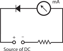
19-6 Illustration for Quiz Question 15.
(a) reverse-biased beyond the avalanche voltage.
(b) reverse-biased below the avalanche voltage.
(c) forward-biased beyond the forward breakover voltage.
(d) forward-biased at less than the forward breakover voltage.
16. In the circuit of Fig. 19-7, the milliammeter (mA) indicates significant current. By examining the polarities of the diode and the DC source, we can see that the diode is
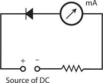
19-7 Illustration for Quiz Question 16.
(a) reverse-biased beyond the avalanche voltage.
(b) reverse-biased below the avalanche voltage.
(c) forward-biased beyond the forward breakover voltage.
(d) forward-biased below the forward breakover voltage.
17. Charge carriers move faster through some semiconductors than others. In general, as the charge-carrier speed increases, so does the maximum
(a) speed at which a device made with that substance can operate.
(b) voltage that the substance can withstand.
(c) current that the substance can handle.
(d) resistance of a component made with that substance.
18. In a P-N junction forward-biased beyond the forward breakover voltage, the junction
(a) is surrounded by a zone devoid of charge carriers.
(b) acts like a capacitor.
(c) does not conduct current.
(d) None of the above
19. Which of the following things commonly serves as a charge carrier in a semiconductor?
(a) An atomic nucleus
(b) A proton
(c) A neutron
(d) An electron
20. Fill in the blank to make the following statement true: “In a semiconductor material, ________ account(s) for most of the current.”
(a) minority carriers
(b) majority carriers
(c) electrons
(d) holes