
8 Special Techniques of Printed Antenna
Dr. Dinesh Kumar Singh
G L Bajaj Institute of Technology and
Management, Greater Noida
Dr. Ganga Prasad Pandey
Pandit Deendayal Petroleum University, Gujarat
Contents
8.2 C-Shaped Reconfigurable Antennas
8.2.1 C-Shaped Antenna with Switchable Wideband Frequency Notch
8.2.3 Design of C Shape Antenna with Switchable Wideband Frequency Notch
8.2.5 Characteristics of the C-Shaped Antenna with a Switchable Wideband Frequency Notch
8.2.6 Other Radiation Characteristics
8.3 Magnetoelectric Dipole Antenna
8.3.3 Characteristics of the Magnetoelectric Dipole Antenna
8.1 Introduction
Printed antennas are available in various shapes and most widely accepted by researchers, scientists, and engineers for various applications; however, they have bandwidth limitations. Since the inception of printed antennas, a number of techniques have been invented to enhance the bandwidth of these antennas. In this chapter, some of the special techniques of designing printed antennas for reconfiguration, polarization, feeding, etc. are discussed. This chapter is broadly divided into two parts; in the first part, two reconfigurable antennas are presented, while the second part presents a circularly polarized wideband magneto-electric dipole (MED) antenna with a defective semicircular patch for C-band applications (4–8 GHz).
The first design presents an antenna with frequency notch characteristics. This section includes two designs of reconfigurable antennas. In the first design, a novel antenna with frequency notch characteristics is presented. The antenna consists of a C-shaped Microstrip antenna with two symmetrical notches and a rectangular parasitic patch. The antenna has tunable property due to the integrated PIN diode. The second design consists of a simple radiating truncated rectangular patch with a cross-shaped slit and a ground plane embedded with L-shaped slit. The antenna produces two separate impedance bandwidths with three senses of polarization, namely, right-hand circular polarization, left-hand circular polarization, and linear polarization. The PIN diode is used to reconfigure the L-shaped slit in the ground plane. The antenna generates a dual band behavior with multiple circularly and linearly polarized bands.
The second part presents a circularly polarized wideband magneto-electric dipole (MED) antenna with a defective semicircular patch for C-band applications (4–8 GHz). In the proposed design, to get proper impedance matching and stable gain, a pair of folded vertical patches is shorted between a pair of defected semicircular patches and minimum ground plane. The defected semicircular patches work as electric dipoles, while the vertical patches work as magnetic dipoles.
8.2 C-Shaped Reconfigurable Antennas
A reconfigurable antenna is useful in the changing the operating requirements to maximize the antenna performance due to its reconfigurable capabilities. The reconfigurable antenna has a capability to modify its frequency, polarization, and radiation properties in a controlled and reversible manner. Reconfigurable behavior can be obtained by modifying the antenna structure using different mechanisms such as PIN diodes, varactors, RF switches, and tunable materials. These mechanisms enable the intentional redistribution of the surface currents producing reversible modifications of the antenna properties. The reconfigurable antenna is useful in applications where multiple antennas are required. Multiple antennas can be replaced by a single reconfigurable antenna.
8.2.1 C-Shaped Antenna with Switchable Wideband Frequency Notch
The number of bands are increasing day by day with multiple high-speed services. These services need a high bandwidth and need to be separated from each other to avoid interference between channels. There are two primary design requirements for this. The first is an antenna design with frequency notch and the second is an antenna design with high cross-polarization attenuation. The notched frequency band refers to frequency response with a small stopband and cross-polarization refers to the orthonormal orientation of electric fields (vertical and horizontal). The adjacent bands in a satellite are isolated by notched frequency bands and polarization, that is, if the first channel is vertically polarized, the second will be horizontally polarized and the third will again be vertically polarized, and so on. This provides isolation among various channels. The antennas designed for multibands with a stopband in between are known as frequency notched antennas. For instance, three bands are allocated for Wireless Local Area Network (WLAN) 2.4 GHz (2,400–2,484 MHz), 5.2 GHz (5,150–5,350 MHz), and 5.8 GHz (5,725–5,825 MHz). Worldwide, the WiMAX system operates at the frequency bands of 2.5 GHz (2,500–2,690 MHz), 3.5 GHz (3,400–3,690 MHz), and 5.8 GHz (5,250–5,825 MHz). Another high-speed WLAN service of 1 Gbps speed is under development (IEEE 802.11.ac), which is to operate around 5 GHz.
Many techniques have been proposed for designing band-notched antennas. The simplest method is to etch slots on the radiating patch of the antenna, such as U-shaped slots [1], L-shaped slots [2,3], and V-shaped slots [4]. An effective way of achieving a UWB compact frequency notched antenna is the use of a split ring resonator (SRR) [5, 6 and 7]. A square split ring resonator is used in [5], while in [6], a slot-type SRR has been used to design an ultrawideband notched antenna. Multiple notched frequency bands have been implemented with an SRR below feed line in [7], with simple slots in [8], and using a half-mode substrate in [9]. A frequency notched printed slot antenna has been implemented in [10], while a compact antenna is designed using fractal geometry in [11]. Instead of using the conventional fractal geometry such as Koch curves, Sierpinski triangles, and Minkowski fractals, a Koch-curve-shaped slot has been employed to achieve a compact geometry with frequency notch characteristics.
The coaxial probe feed is one of the most popular feeding techniques for electrically thick substrates, but the inductance of the probe creates impedance mismatch and causes low bandwidth. The inductance of the probe is compensated for by cutting slots on the patch, using an L-shaped strip feed [12] or by introducing a capacitive feed strip [13,14]. But these configurations create theoretical complexity in terms of analysis apart from the mechanical alignment issues while assembling and hence may increase the production cost. Capacitive feed provides a simple and ultrawide impedance matching by compensating for probe inductance with its capacitance.
A C-shaped antenna may be described as an RMSA with rectangular notch at one of the edges [15]. This is a very popular technique to achieve dual band [16] and wideband [17] characteristics.
In this design, a new technique has been presented to achieve a frequency notched antenna. A simpler capacitive coupling technique has been employed to get ultrawideband characteristics. A PIN diode has been used so that the antenna operates in ultrawide band as well as dual band with a frequency notched antenna. The gain and other radiation characteristics are normal, while the cross-polarization attenuation is very high.
8.2.2 Multiband Multipolarized Reconfigurable Circularly Polarized Monopole Antenna with a Simple Biasing Network
In recent years, circularly polarized monopole antennas have attracted a great deal of attention for the current wireless communication system, as circular polarization (CP) plays a very important role in improving the quality of the received signal [18]. These applications include the C-band communication satellite from 5.925 to 6.425 GHz for their uplink and amateur satellite operations in the frequency range of 5.830 to 5.850 GHz for downlinks. The X-band uplink frequency band uses 7.9–8.4 GHz for military communication systems. The traffic light crossing detector operates at 10.4 GHz. In Ireland, Saudi Arabia, and Canada, terrestrial communication uses the bandwidth of 10.15–10.7 GHz. The usage of multiple antennas for achieving different CP radiations will make the system complex. Hence, as per the demand of the next-generation communication systems, single multiband circularly polarized antennas can be used to reduce the complexity of the system. Therefore, designing such antennas have attracted a great deal of attention among the researchers. However, designing such antennas is challenging when the number of operating CP frequency bands increases. Generally, a monopole antenna generates linearly polarized radiation. Hence, it is difficult to radiate CP waves which were produced by two near-degenerated orthogonal resonant modes of equal amplitude with opposite phase differences. In [19], CP is generated in the triangular patch by using a Koch curve. The axial ratio bandwidth is about 1.3%. A triple proximity-fed microstrip antenna gives the CP with an axial ratio bandwidth of 0.70% for the L-band [20]. In [21], an elliptical microstrip antenna with proximity coupling is used to excite CP waves with an axial ratio bandwidth of about 0.85%. In [22], a simple circularly polarized antenna is presented. The CP operation is obtained by using an open slot having an open width at the lower side of the model. In [23], a slot antenna with straight feed is presented. An SRR-inspired structure is used to obtain the circular polarization. Wideband high gain circularly polarized antennas are proposed in [24]. The use of feed and parasitic patches makes the structure complex. Many CP monopole antennas were proposed for various applications in wireless communication [25, 26, 27 and 28]. In [25], an asymmetrically shaped radiator fed by a microstrip line and a limited ground plane is presented. In [26], the CP is achieved by loading four cylinders that are perpendicular to the substrate of the microstrip antenna near the edge of the circular patch. In [27], by using a rectangular dual-loop technology and tuning the separation between the ground plane and antenna, the monopole antenna produces a CP. In [28], an asymmetric antenna geometry is used to obtain the wideband CP. However, CP monopole antennas mentioned above focus on single CP band operation. Dual band CP has been investigated in [29, 30, 31, 32 and 33]. The antenna presented in [29] composed of a partial ground plane and a Y-shaped radiating patch that consists of two unequal monopole arms and a modified circle. The dual CP is obtained with two unequal monopole arms and a modified circle with an axial ratio bandwidth of 3.8% and 6.8%. In [30], dual CP is obtained by embedding an inverted-L slit in the ground plane. A halved falcate-shaped dual-broadband CP printed monopole antenna is proposed in [31]. To generate dual CP, two halved falcate-shaped antennas were used to generate orthogonal modes and three stubs in the ground plane were used to give 90 degree phase difference. A novel monopole antenna with dual CP consisting of a radiating patch composed of an annular-ring linked by a square ring over the corner and a ground plane with embedded rectangular slit was proposed in [32]. In [33], the dual band CP operations are realized by using two parallel monopoles – one curved monopole and one fork-shaped monopole – and a crane-shaped strip is placed on the ground plane. A dual-feed, dual-band-stacked, CP patch antenna system is presented in [34]. The use of dual feed and stacking gives the structure complex. Triple band CP radiations are presented in [35,36]. In [35], a hexagonal slot antenna with L-shaped slits is presented with a narrow 3 dB axial ratio bandwidth of 1.7%, 3.86%, and 5.23%, while 3 dB axial ratio bandwidths of 9.8%, 4.6%, and 2.8% have been achieved in [36]. The complexity of these two designs [35,36] may hinder the integration of antennas in different applications. In [37], an inverted U-shaped radiator rotated by 45° around the horizontal axis is used to generate the triple band CP.
Recently, reconfigurable CP antennas have attracted significant attention. The PIN diodes are switched in different states to obtain the tunable property of the antenna [38]; this technique is also used to generate a reconfigurable CP microstrip antenna [39]. The authors in [40] proposed a dual feed microstrip patch antenna with frequency and polarization reconfigurability. The frequency and polarization reconfigurability are achieved by using six PIN diodes. The design is complex because of the six PIN diodes and complex biasing circuits. A frequency- and polarization-reconfigurable antenna using PIN diodes is designed in [41]. PIN diodes are commonly used as switching devices for RF and microwave application systems, as they have the advantages of low insertion loss, good isolation, and low cost [42]. It has been observed from literature reviews that mainly two considerable problems are often encountered in reconfigurable CP antenna designs. The excessive diodes will lead to a complex dc-bias network [19,43], providing independent bias for each diode by some special mechanism, such as using capacitors [44].
In this design, a very simple monopole antenna with reconfigurable multiband CP operations is presented. The antenna has overcome the abovementioned two problems of the reconfigurable CP antenna. The antenna generates right-hand circular polarization (RHCP), left-hand circular polarization (LHCP), and linear polarization (LP) in different bands with a simple biasing network without making the system complex. By removing the triangular portion at the lower edges of the rectangular radiating patch and embedding the cross-shaped slit at the right lower edge and L-shaped slit in the ground plane, the antenna provides two CP bands with three LP bands in the OFF state and three CP bands with three LP bands in the ON state of the PIN diode. The reconfigurable CP is achieved by using a PIN diode on the L-shaped slit in the ground plane. The multiband CP operation is obtained by controlling the ON/OFF state of the diode. The antenna is suitable for many applications such as traffic light crossing detectors at 10.4 GHz, C-band communication satellites for their uplink from 5.925 to 6.425 GHz, amateur satellite operations for downlinks from 5.830 to 5.850 GHz, terrestrial communication from 10.15 to 10.7 GHz, and X-band uplink frequency band from 7.9 to 8.4 GHz for military communication systems.
8.2.3 Design of C Shape Antenna with Switchable Wideband Frequency Notch
The antenna design is divided into three parts to examine the response at various phases. First, a capacitive-coupled C-shaped antenna is investigated. Two notches are cut symmetrically in the structure to introduce a new resonant frequency in its frequency response, and finally a parasitic rectangular patch is connected to the C-shaped microstrip antenna (CSMSA) via the PIN diode. The ON condition of the diode is implemented through a connection while the OFF condition is without any strip. The final antenna structure is shown in Figure 8.1. Figure 8.2a shows the fabricated antenna when the PIN diode is OFF, while Figure 8.2b shows when the diode is ON. The simulation is carried out on IE3D software and the measurements are taken using an Agilent N5230 vector network analyzer. The antenna is fabricated on an RT Duroid 6002 substrate with a dielectric constant of 2.94 and a loss tangent of 0.0012. The thickness of the substrate is 0.76 mm, which is raised by 6 mm in air. The other dimensions of the antenna are given in Table 8.1.

FIGURE 8.1 Schematic of the proposed antenna.

FIGURE 8.2 Fabricated antenna.
|
Value |
|---|---|
Substrate dielectric constant (εr) |
3.0 |
Substrate height (h1) |
0.76 mm |
Air height (h2) |
6 mm |
Feed width (wf) |
1.2 mm |
Feed length (Lf) |
3.7 mm |
Spacing between feed and patch (d) |
0.5 mm |
Main patch size (L × W) |
15.5 mm × 25.5 mm |
Parasitic patch size (L1 × W1) |
4.3 mm × 7.75 mm |
Notch size (ls × ws) |
4.75 mm × 1 mm |
Spacing between the C-shaped antenna and the rectangular patch (d1) |
1.0 mm |
Width of each side wings of the C-shaped antenna (W2) |
7.875 mm |
8.2.4 Multiband Multipolarized Reconfigurable Circularly Polarized Monopole Antenna with a Simple Biasing Network
The proposed reconfigurable multiband circularly polarized microstrip-fed monopole antenna is shown in Figure 8.3. The proposed CP antenna is designed and fabricated on an FR4 substrate of thickness h = 1. 6 mm and relative permittivity εr = 4.4. An SMA connector is connected to a microstrip feed line of width W1 and length L1, which is connected to an impedance transformer of width W2 and length L2. The approximate value of the length of the monopole antenna radiating strip is given by the following formula [30]:

FIGURE 8.3 Schematic of the proposed antenna (a) top view (b) side view.
where εeff = (εr + 1)/2, c is the speed of light, λ0 is the free space wavelength at the monopole resonant frequency f0 and εeff is the approximated effective dielectric constant. The dimensions of the rectangular radiator of the antenna are L0 × W0. Generally, a monopole antenna generates either vertical or horizontal linearly polarized radiations and finds difficulty to generate two orthogonal current components with an equal amplitude and 90° phase differences. CP radiations can be generated by introducing a perturbation segment into a linearly polarized antenna; the linearly polarized orthogonal modes can be converted to LHCP or RHCP. Thus, to meet the desired CP conditions, a triangular portion is cut from the left lower edge of the radiator patch to adjust for the impedance matching and an L-shaped slot is embedded in the ground plane to generate the dual CP radiation [45]. Further, to produce 90° phase differences between the currents at distinct frequencies, a triangular portion is removed from the right lower corner of the monopole radiator and a cross-shaped slit is introduced on the truncated right lower edge of the radiator patch to disturb the surface current on the patch. The antenna exhibits a dual band behavior with two different CP radiations. To design the reconfigurable CP, a PIN diode as the switching component is used. The reconfigurable CP antenna has an L-shaped slot with a PIN diode (SMP1320-079) in the ground plane, as shown in Figure 8.3. When a positive voltage (V1 = +0.73 V) is applied, a diode acts as a short circuit (ON state) with a small resistance (0.9 Ω). When a zero voltage is applied, the diode acts as an open circuit (OFF state). The geometry of the antenna varied with the ON/OFF state of the PIN diode, providing the proposed antenna with switchable CP bands in accordance with the change in geometry. A dc bias circuit is used to control the ON/OFF state of the PIN diode as shown in Figure 8.3a. A narrow slit in the ground plane is used for dc isolation. These two isolated portions of the divided ground plane are connected to each other in an ac manner by the use of capacitors. Since the bias circuit is located on the ground plane, an RF choke is not required to isolate the bias circuit from the radiation element, resulting in a reduced effect on the radiation by the bias circuit [46]. During the simulation, the ON state of the PIN diode is implemented with a copper link of length 1 mm and width 1 mm. The detailed dimensions of the proposed reconfigurable multiband CP antenna are listed in Table 8.2.
Parameters |
L0 |
W0 |
L1 |
L2 |
L3 |
W1 |
W2 |
B1 |
|---|---|---|---|---|---|---|---|---|
Values (mm) |
23.5 |
12 |
6.0 |
9.5 |
26 |
3.0 |
2.4 |
5.0 |
Parameters |
l1 |
l2 |
S1 |
S2 |
S3 |
S4 |
S5 |
B2 |
Values (mm) |
7.0 |
6.0 |
1.0 |
6.0 |
11.0 |
4.7 |
7.0 |
2.5 |
The evolution of various stages involved in the proposed antenna design is shown in Figure 8.4, while the reflection coefficients and axial ratios obtained in each stage are shown in Figures 8.5 and 8.6, respectively. The basic element used in the antenna design is a conventional rectangular patch and ground plane (Ant1). From Figure 8.5, it can be seen that in this case, three resonant modes are obtained at 7.75, 10.42, and 14.92 GHz. Ant1 exhibits the linear polarization (3-dB axial ratio > 3) as depicted in Figure 8.6. Ant2 shows that resonance frequencies shifted downward and operated at multiband frequencies due to modification of the ground plane by embedding an L-shaped slot in the ground plane (Ant2). The dual CP bands at the center frequencies 3.34 and 8.58 GHz are obtained as shown in Figure 8.6 (Ant2). The upper CP band is not within the operating band. Ant3 indicates that the removal of the triangular portion from the lower edges of both sides of the radiator patch provides two wideband operations and three CP operations with a small ARBW as shown in Figures 8.5 and 8.6, respectively. Finally, the radiating patch is modified by cutting a cross-shaped slot on the truncated right lower edge to obtain dual band characteristics and dual band CP behavior with a good ARBW. The proposed antenna is simulated by the Method of Moments–based IE3D simulator. Figure 8.7 shows the fabricated prototype of the antenna.

FIGURE 8.4 Antenna geometry evolution process of the proposed antenna.
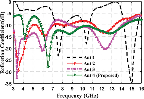
FIGURE 8.5 Simulated reflection coefficient for the various antenna configurations.

FIGURE 8.6 Simulated axial ratio for the various antenna configurations.

FIGURE 8.7 Fabricated prototype of the proposed antenna.
8.2.5 Characteristics of the C-Shaped Antenna with a Switchable Wideband Frequency Notch
A capacitive coupled C-shaped antenna is designed to operate in the frequency band of 5–8 GHz. The antenna exhibits two resonance frequencies. To achieve a sharper frequency response, two notches are cut symmetrically in the C-shaped microstrip antenna. Figure 8.8 shows the return loss variation of CSMSA with and without symmetrical notches. Clearly, a new resonant frequency is added at the higher side of the response.
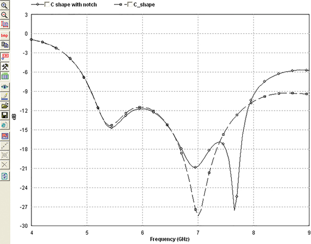
FIGURE 8.8 Variation in return loss with frequency.
After the cutting of notches, a parasitic patch is kept in the etched portion (mouth) of the CSMSA. The effect of putting the rectangular parasitic patch is shown in Figure 8.9. It is clear from the figure that the response remains almost unchanged after placing the parasitic rectangular patch. The slight shift in the response may be due to the mutual coupling between the structures.
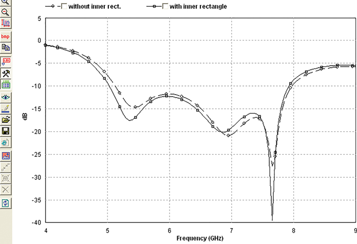
FIGURE 8.9 Variation in return loss with frequency with and without inner parasitic element.
After placing a parasitic element to the structure, a PIN diode (model HSMP-3860) is connected between them. The PIN diode is implemented by 1.2 mm× 1 mm through connection. The simulated and measured return loss variation when the PIN diode is OFF is shown in Figure 8.10. There is an acceptable resemblance between them. When the diode is ON, a wide frequency band around 5 GHz is notched, as shown in Figure 8.11. In practical applications, a sharp frequency notch is desirable to isolate the two bands. Here, a simple wide frequency notch is adopted to isolate the two bands. Thus, the antenna can be used both for ultrawide band and for narrow band. In fact, this notch appeared due to a shift in the lower resonant frequency towards the lower frequency spectrum and an impedance mismatch in between. This decrease in frequency was due to the enlarged current path.

FIGURE 8.10 Simulated and measured results of tunable CSMSA when the diode is OFF.

FIGURE 8.11 Return loss variation when the diode is ON.
The current distribution at old and new (shifted) resonant frequencies is shown in Figure 8.12.

FIGURE 8.12 Current distribution (a) at 5.6 GHz when the diode OFF and (b) at 4.7 GHz when the diode ON.
To observe the behavior of the resonant frequency of the newly formed narrow band, the return loss is taken for different lengths of the parasitic rectangle, as shown in Figure 8.13. It is clear from the figure that as the length of the rectangle increases, the resonant frequency decreases, which shows the path length of current lines.
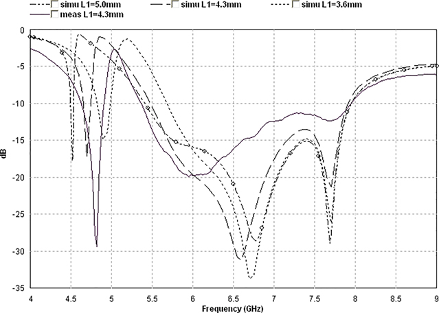
FIGURE 8.13 Return loss variation for different lengths of inner parasitic rectangle when the diode is ON.
8.2.6 Other Radiation Characteristics
Figure 8.14 shows the gain of the tunable C-shaped microstrip antenna. It is observed from the figure that a better gain is obtained because of the better matching when the diode is OFF. A sharp fall in gain is observed in the stop band when the diode is ON. Figure 8.15 shows the radiation pattern at various resonant frequencies for the ON and OFF conditions of the PIN diode in the E-plane. It is observed from the figure that the radiation pattern is the same for 5.6, 6.5, and 7.7 GHz, which are in the same band of operation. When the band of operation changes (at 4.7 GHz), the main lobe of beam rotates from −10.48° to −30.3°, which is again due to the current path lines flowing in the inner rectangle. Figure 8.16 shows the current lines for 6.5 and 7.7 GHz when the diode is OFF and ON. When the diode is OFF, there is no coupling between the C-shaped antenna and the rectangle. In the ON condition, a little coupling is observed at 6.5 GHz, while being negligible at 7.7 GHz. This is why the shift in the second resonant frequency is the most (Figure 8.11).

FIGURE 8.14 Variation in the gain of the tunable C-shaped microstrip antenna.

FIGURE 8.15 Radiation pattern of the tunable microstrip antenna at (a) 5.6 GHz (OFF) and 4.7 GHz (ON), (b) 6.5 GHz (both) and (c) 7.7 GHz (both).

FIGURE 8.16 Current distribution at (a) 6.5 GHz and (b) 7.7 GHz.

FIGURE 8.17 Copolar and cross-polar radiation pattern at 6.5 GHz.
8.2.7 Multiband Multipolarized Reconfigurable Circularly Polarized Monopole Antenna with a Simple Biasing Network
The measured and simulated reflection coefficients and the measured and simulated axial ratios with the OFF state of the diode are shown in Figure 8.18a and b, respectively. The proposed antenna exhibits a dual band behavior in the OFF state of the diode having an impedance bandwidth of 10.22% and 83.43% in the frequency range of 3.99–4.42 GHz and 5.84–14.20 GHz, respectively. In the OFF state of the diode, the antenna has successfully achieved two CP bands operation with a 3-dB axial ratio bandwidth of 9.83% and 13.73% in the frequency range of 5.79–6.39 GHz (CP1) and 8.49–9.74 GHz (CP2), respectively, and three LP bands in the frequency range of 3.99–4.42 GHz, 6.40–8.48 GHz and 9.75–14.20 GHz. The measured and simulated reflection coefficients for the ON state of the diode are shown in Figure 8.19a. Figure 8.19b illustrates the measured and simulated axial ratios in the ON state of the diode. In the ON state, the antenna also exhibits a dual band behavior with an impedance bandwidth of 49.10% and 21.31% in the frequency range of 7.20–11.04 GHz and 12.66–15.37 GHz, respectively. When the diode is set to the ON state, a switchable CP antenna is obtained. The antenna attains triple band CP operations with a 3-dB axial ratio bandwidth of 6.49%, 8.45% and 2% in the frequency range of 7.90–8.43 GHz (CP3), 10.08–10.97 GHz (CP4) and 12.87–13.13 GHz (CP5), respectively, and three LP bands in the frequency range of 7.20–7.89 GHz, 8.44–10.07 GHz and 13.34–15.37 GHz. The measured results are within reasonable agreement with simulated results. The differences between the simulated and measured results are due to the fabrication imperfections. They are also the reason that the simulation uses an open gap and a copper strip to represent the equivalent circuits of the PIN diode in the OFF and ON states, respectively. The reflection coefficient is tested by an Agilent5230A vector network analyzer, and radiation performances are measured in an anechoic chamber.

FIGURE 8.18 (a) Simulated and measured reflection coefficients of the proposed antenna in the OFF state of the diode. (b) Simulated and measured axial ratios of the proposed antenna in the OFF state of the diode.

FIGURE 8.19 (a) Simulated and measured reflection coefficients of the proposed antenna in the ON state of the diode. (b) Simulated and measured axial ratios of the proposed antenna in the ON state of the diode.
The total gain of the circularly polarized antenna can be given as [28,45,47]
where GTV is the partial power gain with respect to linearly vertical polarization and GHV is the partial power gain with respect to linearly horizontal polarization. A linearly polarized standard horn antenna with a calibrated gain is used in the measurement of GTV and GHV. The simulated and measured gains with the ON/OFF state of the diode are shown in Figure 8.20. The differences in the measured and simulated results of the gain are due to the loss in the PIN diode and measurement error. The peak gain of the antenna in the 3-dB axial ratio bands are 1.30 and −0.60 dBic at the center frequencies of the CP bands, respectively, for the OFF state, while 1.41, −0.41 and −0.86 dBic at the center frequencies of CP bands, respectively, for the ON state of the diode. The simulated and measured radiation efficiencies of the proposed antenna in the ON and OFF states of the PIN diode are shown in Figure 8.21. The radiation efficiencies remain in the range of 65 ± 5%. The measured and simulated results agree well within the acceptable limit. Figure 8.22a and b plot the simulated and measured normalized RHCP and LHCP radiation patterns at the center frequencies of the CP radiations for the OFF state of the diode, while Figure 8.23a–c plot the radiation patterns at the center frequencies for the ON state of the diode in the two orthogonal planes (E-plane (Φ = 0°) and H-plane (Φ = 90°)). It can be seen that good LHCP and RHCP are observed at the center frequencies of the CP bands CP1 and CP2, respectively, for the OFF state of the diode. In the ON state of the diode, the RHCP, RHCP, and LHCP wave are observed at the center frequencies of the CP bands CP3, CP4, and CP5, respectively.

FIGURE 8.20 Simulated and measured gains of the proposed antenna in the ON and OFF states of the diode.

FIGURE 8.21 Simulated and measured radiation efficiencies of the proposed antenna in the ON and OFF states of the diode.
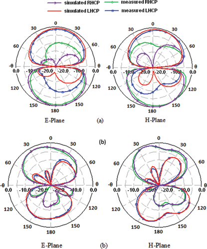
FIGURE 8.22 Simulated and measured normalized LHCP and RHCP radiation patterns at the center frequencies of the CP band when the diode is OFF (a) at 6.1 GHz and (b) at 9.1 GHz.

FIGURE 8.23 Simulated and measured normalized LHCP and RHCP radiation patterns at the center frequencies of CP band when the diode is ON (a) at 8.43 GHz, (b) at 10.52 GHz and (c) at 13.00GHz.
8.2.8 Radiation Mechanism
In order to understand the operating mechanism and how CP operations are obtained, the simulated current distribution at center frequencies of different CP radiations for t = 0, t = T/4, 2T/4 and 3T/4(T = time period) are shown in Figures 8.24 and 8.25 in the diode OFF and ON state, respectively. At 6.1 GHz, the resultant of the surface current is at 257.5° and clockwise rotation of surface currents at different time frames clearly indicates LHCP. The L-shaped slit in the ground plane and cross-shaped slit in the patch are responsible for generating circularly polarized waves. At 9.1 GHz, the resultant surface current is due to the patch and L-shaped embedded ground plane is about 45° at t = 0 and rotates anticlockwise and the antenna radiates LHCP waves with time. In the diode ON condition as shown in Figure 8.25, at 8.43 GHz, the currents at the L-shaped embedded ground plane are cancelled out by each other, and the resultant current is due to the cross-shaped slit at t = T/4.

FIGURE 8.24 Surface current distribution at the center frequency of the CP bands when the diode is OFF (a) at 6.1 GHz and (b) at 9.1 GHz.
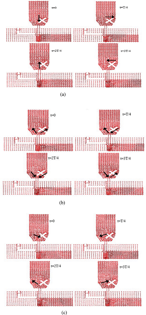
FIGURE 8.25 Surface current distribution at the center frequency of the CP bands when the diode is ON (a) at 8.43 GHz, (b) at 10.525 GHz, and (c) at 13.00 GHz.
The field rotates in the anticlockwise direction, which results in exciting an RHCP radiation. At 10.525 GHz, the cross-shaped slit in the radiator patch is responsible for generating the RHCP radiation, as the surface currents rotate in anticlockwise manner. The clockwise rotation of the resulting surface current is responsible for producing the LHCP mode, at 13.00 GHz. As observed from the above figures, in the ON state of the diode, the surface currents in the L-shaped slotted ground is cancelled out and the resultant current is zero. The only CP is produced due to the asymmetric cross-shaped slit in the patch. Table 8.3 summarizes the sense of polarization of reconfigurable CP bands.
Diode States |
|
Band 1 |
Band 2 |
Band 3 |
Band 3 |
Band 5 |
Band 6 |
|---|---|---|---|---|---|---|---|
OFF |
Senses of polarization |
LHCP |
RHCP |
LP1 |
LP2 |
LP3 |
– |
Frequency range (GHz) |
5.79–6.39 |
8.49–9.74 |
3.99–4.42 |
6.40–8.48 |
9.75–14.20 |
– |
|
ON |
Senses of polarization |
RHCP |
RHCP |
LHCP |
LP1 |
LP2 |
LP3 |
Frequency range (GHz) |
7.90–8.43 |
10.08–10.97 |
12.87–13.13 |
7.20–7.89 |
8.44–10.07 |
13.34–15.37 |
Reference |
Antenna Type |
No. of Feeds |
No. of Diodes |
Biasing Circuit |
Reconfigurable Properties |
Senses of Polarization |
No. of Bands |
|---|---|---|---|---|---|---|---|
[20] |
3 |
n.a. |
n.a |
NO |
CP |
01 |
|
[22] |
Monopole |
1 |
n.a. |
n.a. |
NO |
CP |
01 |
[24] |
Multilayer with air gap |
2 |
n.a. |
n.a. |
NO |
CP |
01 |
[34] |
Multilayer |
2 |
n.a. |
n.a. |
NO |
CP |
02 |
[38] |
C-shaped microstrip antenna |
1 |
1 |
Complex |
Yes |
LP |
03 |
[40] |
Square microstrip antenna |
02 |
06 |
Complex |
Yes |
LP CP |
02 02 |
[41] |
Center-fed circular cavity |
01 |
24 |
Complex |
Yes |
LP |
06 |
[48] |
Square microstrip antenna |
01 |
04 |
Complex |
Yes |
LP CP |
02 02 |
[46] |
Square microstrip antenna |
01 |
08 |
Simple |
Yes |
CP |
02 |
Proposed work |
Monopole antenna |
01 |
01 |
Simple |
Yes |
LP CP |
06 05 |
8.2.9 Parametric Study
In order to analyze the operational performance of the presented antenna, the vital parameters are investigated to evaluate their impacts on the antenna. The parameters of cross-shaped slot and L-shaped slit are examined to find their impacts on the antenna performance and are illustrated in Figures 8.26 and 8.27, respectively. The parametric study is carried out by varying the parameters S2, S3, S4, S5, l1, and l2 to examine their effects on the reflection coefficients and axial ratio. It can be seen from Figure 8.26a–e, that by increasing and decreasing S2, S3, S4, S5, and l2, little change is observed on the lower band and a very slight change is observed on the upper band of the reflection coefficient. The reflection coefficient is strongly dependent on l2 as shown in Figure 8.26f. By decreasing the length l2, the whole band is disturbed and reflection coefficient is above −10 dB.
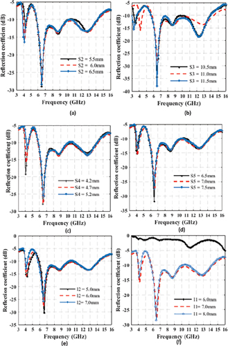
FIGURE 8.26 Parametric studies of the proposed structure: (a) variation in S2, (b) variation in S3, (c) variation in S4, (d) variation in S5, (e) variation in l2, and (f) variation in l1.

FIGURE 8.27 Parametric studies of the proposed structure: (a) variation in S2, (b) variation in S4, (c) variation in S5, (d) variation in l2, (e) variation in S3, and (f) variation in l1.
The changes in CP performances by varying the parameters S2, S3, S4, S5, l1, and l2 are shown in Figure 8.27. The CP performances are slightly affected by the change in the value of S2, S4, S5, and l2 as shown in Figure 8.27a–d, respectively. The CP bands strongly depend on the value of S3 as shown in Figure 8.27e. By increasing and decreasing S3, four CP bands with small ARBW are obtained, out of which two CP bands are not lying in the operating bands. An increase in the length l1 has little effect on the CP operation at lower and upper bands, while a decrease in l1shows that the CP bands shifted upward as shown in Figure 8.27f.
8.3 Magnetoelectric Dipole Antenna
The magnetoelectric (ME) dipole antenna is a combination of an electric dipole and a magnetic dipole. The ME antenna is a complementary antenna concept that has a symmetrical radiation pattern in both E- and H-planes with a broad beam width. The vertical metallic walls act as a magnetic dipole, which is shorted with the ground plane at one end and the planer metallic electric dipole patch in another. A proximity-coupled feed is used to excite the ME dipole antenna, which performs as a combination of an electric dipole and a magnetic dipole. The ME dipole antenna exhibits various advantages, such as a broad impedance bandwidth, a stable gain, and a stable radiation pattern with low cross-polarization and back radiation levels over the operating frequencies.
Thanks to the speedy development of wireless communication systems, the focus of many researchers has been the development of advanced antennas to meet the demands of latest applications with attributes such as broadband, symmetrical radiation pattern, high gain, and compact size. Patch antennas are suitable candidates that satisfy all these attributes as well as easy fabrication; however, they encounter the problem of narrow bandwidth [49]. To achieve a broad bandwidth, Clavin et al. have presented antennas based on the complementary antenna concept, which have shown a symmetrical radiation pattern in the E- and H-planes with a broad beam width and stable gain [50,51]. In [52], the magnetoelectric dipole (MED) antenna has been presented for a femto cell base station with a rectangular ground and defected patch. The antenna has achieved an impedance bandwidth of 51.9%, but the design suffers from large size. Further, to make low-profile antennas, the height of MED antennas is decreased by implementing the folded structure as presented in [53] and the regular square-shaped ground is replaced by minimum-sized ground plane [54]. The authors in [55] have presented a low-profile antenna with a high gain of 9.2 ± 1.1 dBi and an impedance bandwidth of 28.2%. In [56], the impedance bandwidth of a broadband dual polarized antenna is enhanced by the use of an L-shaped cavity–backed ground plane with proximity coupling, but it uses a large size cavity to improve the isolation between two ports. A new feeding structure—a combination of inverted U-shaped and meandering T-shaped feeds—presented in [57] has been used to design a printed dual band MED antenna. But it has exhibited a small gain of 3 ± 0.5 dBi only.
These wideband antennas are capable of meeting the demands of the current wireless system, but incorporating the features of circular polarization (CP) will make these antennas more efficient. Therefore, CP antennas are getting more fascinating and promising within wireless systems, such as satellite communications [58], global positioning system [59], and radio frequency identification [60], because of their stable reception of the signal, multipath interference suppression, and additional immunity towards the polarization mismatching [61]. The fundamental operating principle of a CP antenna is the radiation of two orthogonal field components with equal amplitude and in-phase quadrature. Various techniques such as single-probe feed method [62], aperture-coupled feed method [63], and dual-fed structure method [64,65] have been used to achieve the CP in microstrip antennas. The first two methods [62,63] suffered from a narrow axial ratio (AR) bandwidth, while the later methods [64,65] have shown an AR bandwidth of more than 30%. However, these methods occupy a larger area and a complicated feeding structure; as a result, the design becomes bulky and complex. To overcome these problems, simple techniques are available to generate the CP operation, for example, by cutting the slots, inserting the slits in the patch and corner truncations [66, 67 and 68]. In [69], a quad-band CP antenna with an inclined slot and corner truncations was presented for C-band applications. The antenna exhibits an impedance bandwidth of 55.46%, but its structure is complicated due to the stacked structure and exhibits very narrow CP bands. An ultra-wideband antenna with the CP characteristics is presented in [70]. To achieve the CP, the rectangular slot is truncated by two circular arcs of unequal radii. In [71], a reconfigurable circularly polarized capacitive-coupled microstrip antenna was considered to enhance the operating bandwidth of the antenna by the application of a PIN diode–based switching system, but it lacks an immediate response while the switching is applied. Another conventional approach to obtain the CP is a crossover dipole antenna in which two crossed dipoles of different lengths are selected to produce two orthogonal fields with an equal amplitude and a phase difference of 90° [72]. However, this method gives only a narrow impedance and AR bandwidth [72]. The impedance bandwidth is enhanced by 20% with the use of a crossed bowtie dipole design as proposed in [73]. The design also shows an improvement in the AR bandwidth of more than 7%. In [74], the improvement in AR bandwidth is achieved by adding a sequential rotational configuration. Further, the impedance bandwidth has been improved by using cavity-backed wide-open end cross dipole antennas, but the ease of construction is compromised [75]. However, dipole antennas with cavities [75] have a broad impedance bandwidth and good radiation patterns, but the integration of the additional cavities increases the complexity of the design and the radiation pattern on the broadside are not stable.
We herein propose a circularly polarized wideband MED antenna with a defective semicircular patch. The proposed design consists of copper-made horizontal defective semicircular patches, a pair of folded vertical patches, which work as an electric dipole and magnetic dipole, respectively, and a minimum ground plane at the bottom. A single feed and minimum ground have been chosen to maintain the simplicity of the proposed design as well as to avoid the use of a polarizer, which is mandatory for dual-feed design. The proposed antenna exhibits an impedance bandwidth of 60.37% in the frequency range of 3.71–6.91 GHz and a stable gain of 6 ± 0.5 dBic. The CP behavior has been confirmed in the proposed design in the frequency range of 3.71–4.55 GHz by embedding I-shaped slots in inverted symmetry on the semicircular patches at the appropriate positions. The easy fabrication and cheap cost may increase the popularity of the designed antenna.
8.3.1 Antenna Design
The MED antenna is a combination of an electric dipole and a magnetic dipole. The vertical metallic walls act as the magnetic dipole, which is shorted with the ground plane at one end and the horizontal metallic electric dipole patch in the other end. In the proposed MED antenna, defected semicircular shaped horizontal patches are used as electric dipoles and the folded vertical walls as magnetic dipoles. The detailed geometry of the proposed antenna is shown in Figure 8.28. It is a combination of a minimum rectangular ground of dimension GL × GW, a horizontal pair of defected semicircular patches of radius r and two parallel vertically oriented folded walls, which are placed at an optimized distance. The vertical walls are separated by a gap G until height h2, and the gap of 2 L + G is maintained from height h1 to h2. These gaps play a very important role in stabilizing the antenna gain and reduction in the back-lobe radiation. The use of a larger ground plane generally enhances the directivity with restrictions on practical issues, such as installation and bulkiness at the same time. Therefore, a minimum-sized rectangular ground has been used to maintain the compactness of the proposed design; as a result, a rectangular patch of dimension GL × GW is formed at height h2 and a semicircular patch is used at height h1, which also confirms the maximum height of the structure from the ground plane.

FIGURE 8.28 (a) Top view of the proposed antenna. (b) Front view of the proposed antenna.
In order to initiate the CP operation, an I-shaped slot is cut in each semicircular patch with the help of a sharp mechanical tool. These slots have a diagonal symmetry. Due to the I-shaped slots and symmetrical folded structure, the proposed design exhibits wideband CP radiation characteristics. The gap between the extended parts of the I-shaped slots from the flat edge of the semicircular patch is 4 mm. The lower and upper parts of the I-shaped slots on the left side as well as the right side of the semicircular structures are extended until the curved edges to widen the 3-dB AR bandwidth.
To excite the antenna, the SMA connector is connected to the Γ-shaped feed line, which is divided into three segments a, b, and c with the uniform width f. It can be seen from Figure 8.28 that two vertical elements and one horizontal element are combined to make this type of feeding structure. The first segment (segment a) is connected to the inner conductor of the SMA connector, which is separated from one of the vertical walls by 1 mm and the other wall by 11 mm air gaps and acts as an air-filled microstrip line. The open end of this line is connected to the horizontal coupling line (segment b) of the feed line, whereas the other vertical segment of the feed line (segment c) is connected to the horizontal coupling line. The outer conductor of the connector is soldered to the ground to complete the feed loop. When the antenna is excited, the horizontal segment of the feed structure couples the energy to the semicircular defected patches and the other vertical segment is used to compensate for the inductive effect of the horizontal segment. By adjusting the size of the feed, proper impedance matching is obtained with a characteristic impedance of 50 Ω. The resonance of the antenna moves upward and downward with variation in the length b and height c. All the dimensions and parameters of the proposed design are shown in Table 8.5.
Parameters |
Dimension (mm) |
Parameters |
Dimension (mm) |
|---|---|---|---|
GL |
12 |
A |
19 |
GW |
58 |
B |
9.5 |
R |
29 |
C |
12 |
Sℓ |
16 |
D |
1.5 |
Sw |
4.5 |
E |
1.0 |
Sh |
25 |
F |
4.5 |
G |
12 |
h1 |
20 |
L |
30 |
h2 |
10 |
8.3.2 Parametric Studies
The proposed wideband circularly polarized MED antenna can operate in the frequency range of 3.71–6.91 GHz and exhibits an axial ratio bandwidth of 20.60% in the frequency range 3.71–4.55 GHz. Here, the optimization goal is to achieve the CP behavior as well as wideband operation. The parametric study in terms of its various controlling elements is carried out to obtain the optimum values. During optimization, several important parameters are investigated for optimum performance, such as the radius of the semicircular patch (r), the height of the semi-circular patch (h1), the height of the metallic patch (h2), the gap between two magnetic dipoles (G), and the width of I-shaped slots. During the investigation, while one design variable is changed, the other parameters were kept constant. In Figure 8.29, the different values of radius (r) are evaluated to check its impact on the reflection coefficient. It has been observed that the variation in r has a significant effect on the reflection coefficient variation.

FIGURE 8.29 Variation in reflection coefficient for different values of radius (r).
The impedance bandwidth gets narrower and lower frequency point is shifted towards the lower side when r is increased beyond 29 mm. It can also be noted here that at r = 31 mm, the antenna exhibits dual band characteristics. Similarly, the bandwidth is reduced, when r is kept less than 29 mm, but the lower frequency point is shifted upward. However, in both circumstances, the upper cutoff frequency either remains same or decreases. Hence, it is confirmed that the optimum impedance bandwidth is achieved at the value of r = 29 mm.
The height of the semicircular patch (h1) is varied, and the corresponding reflection coefficient is presented in Figure 8.30.

FIGURE 8.30 Variation in reflection coefficient for different values of height (h1).
When h1 is increased beyond 20 mm, the operating band gets distorted, and when h2 is reduced below 20 mm, the impedance bandwidth gets narrower because of a significant decrease in the second and third resonance frequencies and thereby the upper cutoff frequency. When the height (h1) is decreased below 20 mm, the whole operating band moves upward but the resultant bandwidth decreases. Hence, the optimum value of h1 is 20 mm. Here, it is noticeable that lower resonance frequency remains almost unchanged. Figure 8.31 shows the effect of variation in the height of the horizontal rectangular folded patch (h2), which is varied at the intervals of 0.5 mm. Here, the lower resonance frequency is also unaffected by variation in h2. When h2 is increased beyond the design point of 10 mm, the second resonance frequency decreases.
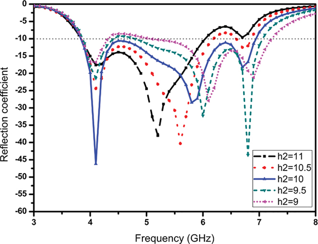
FIGURE 8.31 Variation in reflection coefficient for different values of height (h2).
Moreover, the third resonance point is mismatched and hence, the bandwidth decreases drastically. When it is decreased below the design value, the antenna behaves like a dual band antenna because of the mismatch in the operating band. Therefore, it can be projected here that the height of the folded conducting element of the antenna plays an important role in accomplishing the goal of the proposed design and the optimum value is at h2 = 10 mm.
Figure 8.32 demonstrates the comparison of the reflection coefficient for different values of gap (G) between the two vertical walls.

FIGURE 8.32 Variation in reflection coefficient for different values of gap (G).
Maximum impedance bandwidth has been achieved at G = 12 mm as depicted in the figure. A gradual increment in bandwidth is seen up to 12 mm, beyond which the bandwidth gets narrower and band splits into two bands. At G = 13 mm, the bandwidth is reduced, and hence it can be stated that the distance between two walls is also an important factor to obtain a broad bandwidth. The effect of uniform width (Sw) of the I-shaped slot on axial ratio bandwidth is explained in Figure 8.33.

FIGURE 8.33 Variation in the axial ratio with frequency for different values of slot width (Sw)
The AR bandwidth has changed significantly for instantaneous values of Sw, while Sℓ and Sh are kept constant. When Sw ≤ 4.5 mm, the AR bandwidth gets narrower and for Sw = 5.5 mm, the dual CP band response is shown in the figure; out of these, one CP band does not lie in the operating frequency range. The maximum AR bandwidth is achieved when Sw is fixed at 4.5 mm throughout the I-shaped slot. Embedding I-shaped slots in an extended manner with optimized slot dimensions forced the surface currents to rotate in the counterclockwise direction. Hence, it can be concluded that the optimum AR bandwidth is achieved at Sw = 4.5 mm.
8.3.3 Characteristics of the Magnetoelectric Dipole Antenna
The proposed design has been simulated using an Ansys HFSS simulator and the antenna structure is fabricated by using copper sheet only. The thickness of the copper sheet used in the simulation and the fabrication are kept the same to realize the actual antenna design. The reflection coefficient has been measured in the laboratory by using the Agilent vector network analyzer (VNA) N5230. The simulated and measured values of the reflection coefficients of the proposed antenna are plotted in Figure 8.34, and it can be seen from the figure that the simulated values agree well with the experimental values in the operating frequency range.

FIGURE 8.34 Measured and simulated reflection coefficients of the proposed antenna.
A small deviation in the impedance bandwidth is observed because of the fabrication imperfection and the irregular surface of the metal sheet. The proposed antenna gives an impedance bandwidth of 60.37% from 3.71 to 6.91 GHz, confirming the wideband characteristics of the MED antenna. Furthermore, the antenna has achieved CP characteristics due to the insertion of I-shaped slots in an extended manner on both sides of the semicircular patches. The axial ratio is the ratio of two orthogonal components of the E-field in a given direction and is often used for the antennas in which the desired polarization is circular. The circularly polarized waves can be generated when two orthogonal E-field components with equal amplitude but with in-phase quadrature are radiated. The acceptable value of the axial ratio is less than 3 dB for the patch antennas [39]. Figure 8.35 presents the variation of the measured and simulated AR values with the frequency. It is seen from the figure that a 3 dB AR bandwidth of 20.60% in the frequency range of 3.71 and 4.55 GHz is achieved in the simulation.

FIGURE 8.35 Measured and simulated axial ratios (dB) of the proposed antenna.
However, there is a small deviation in the measured AR bandwidth because of the inaccuracy in measurement, cutting, and finishing. The gain in the antenna along with radiation patterns were measured in an anechoic chamber by using the standard substitution method. After the analysis of outcomes, it is found that the gain is almost constant over the entire CP band as shown in Figure 8.36.
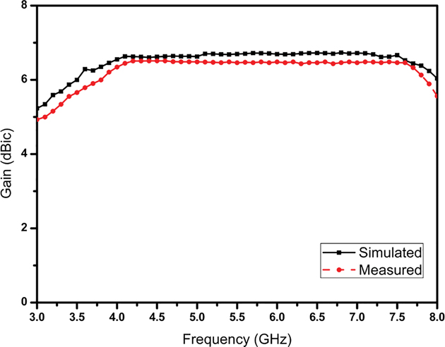
FIGURE 8.36 Measured and simulated peak gains of the proposed antenna.
In general, errors that occur during the measurement is approx. ±0.30 dB, and those further can be minimized by using precision handling processes and precisely calibrated instruments. Simulated and measured results have confirmed that the stable gain of 6 ± 0.5 dBic is accomplished in the operating frequency range of 3.71–6.91 GHz as shown in Figure 8.32. A very small variation has been seen due to errors in anechoic chamber measurement. It is confirmed from Figure 8.37 that the measured radiation efficiency matched well with the simulated result and it is more than 80% in the operating frequency range.

FIGURE 8.37 Measured and simulated radiation efficiencies of the proposed antenna.
To verify the CP behavior of the proposed antenna, the simulated current distributions using the simulator Ansys HFSS at different time periods are shown in Figure 8.38. Here, T is the time period of the signal at operating frequency.

FIGURE 8.38 Current distribution showing the right-hand circular polarization for the center frequency of the CP band at 4.1 GHz at different time intervals, t = 0, t = T/4, t = T/2 and t = 3T/4.
Due to the symmetrical structure, the surface current distributions of the semicircular patch of only one side has been considered for a clear visibility of the vector currents and the same pattern can be viewed on the other side also. At time t = 0, the surface currents on the defected semi-circular surface flow along the direction of θ = 0°, while the direction of the surface currents has changed in the upward direction at t = T/4 in the direction of θ = 90°. Further, the direction of the vector currents is changed to θ = 180° and θ = 270° at time t = T/2 and 3T/4, respectively. It is clear from the current distribution pattern that the direction of vector currents at t = T/2 and 3T/4 are just opposite to the currents at t = 0 and t = T/4, respectively. It is also confirmed that the surface currents on the electric dipole rotate in the anticlockwise direction to authenticate the right-hand circular polarization (RHCP) behavior of the antenna.
To compare the radiation patterns in the xoz (Φ = 0°) and yoz (Φ = 90°) planes, the radiation patterns obtained from simulation and measurement are plotted for the broadside direction at the center frequencies of the CP band and is shown in Figure 8.39a and b, respectively. The obtained results validate the basic characteristic of the ME dipole antenna, as the radiation patterns from simulation and measurement are unidirectional and symmetric in the E-plane and H-plane. Also, it is clearly visible from Fig 8.39 (b) that the magnitude difference between LHCP and RHCP is more than 3 dB, which is a remarkable point to validate the CP behavior of the antenna and confirming the RHCP waves. The experimental results agree well with the simulated results. Moreover, the radiation patterns of the xoz- plane and the yoz-plane are stable and symmetrical.

FIGURE 8.39 (a) Simulated and measured E- and H-plane radiation patterns at the centre frequency of the operating band at 5.3 GHz. (b) Simulated and measured RHCP and LHCP radiation patterns for E- and H-planes at the centre frequency of the CP band at 4.1 GHz.
8.4 Conclusion
In this chapter, two designs of reconfigurable antenna have been discussed. First, a novel antenna with tunable characteristics, wide notch frequency band, and reduced cross-polarization has been designed. The experimental and simulation results match to an acceptable limit. The structure provides dual band when the diode is ON and ultrawide band when the diode is OFF. A wide frequency range around 5 GHz is notched when the diode is ON and frequency band below 5 GHz is notched when the diode is OFF. The other characteristics are normal and stable.
The second design consists of a reconfigurable multiband CP monopole antenna with a simple biasing network. The PIN diode is used to obtain multiband reconfigurable CP radiations. In the OFF state of the diode, the antenna exhibits a dual band behavior with three senses of polarization. LHCP, RHCP and three LP waves are observed. In the ON state of the diode, the antenna again exhibits a dual band behavior and produces other three CP radiations along with three LP radiations. The simple structure of the antenna makes it suitable for many applications, such as in C-band communication satellite for their uplink and amateur satellite operations (CP1), X-band uplink frequency for military communication satellites (CP3), traffic light crossing detector, and terrestrial communications (CP4).
In this part, a wideband circularly polarized MED antenna of semicircular shape embedded with diagonally symmetrical I-shaped slots has been proposed and investigated for C-band applications. In the proposed design, defected semicircular patches are placed horizontally to function as electric dipoles and two vertically oriented folded metallic walls shorted to minimum rectangular ground to act as magnetic dipoles. The Γ-shaped single feed structure is used to excite both dipoles together to achieve symmetric radiation patterns and CP waves are produced with the help of I-shaped slots. The low profile of the structure is maintained by the use of minimum ground and the folded structure. Hence, the proposed antenna is compact in design, including features of wideband behavior and circular polarization. It exhibits an impedance bandwidth of 60.37%, AR bandwidth of 20.60%, and a radiation efficiency of more than 80% within the operating frequency range. The proposed design provides CP characteristics in the frequency range of 3.71–4.55 GHz and a stable peak realized gain of 6 ± 0.5 dBic with a unidirectional radiation pattern in E- and H-planes. All these features made this antenna suitable for 5G Wi-Fi (5.15–5.875 GHz) and C band applications (3.7–4.2 GHz for downlink and 5.93–6.43 GHz for uplink).
References
1. Vuong T. P., Ghiotto A., Duroc Y., Tedjini S. (2007). Design and characteristics of a small U-slotted planar antenna for IR-UWB. Microwave and Optical Technology Letters, 49, 1727–1731.
2. Lee W. S., Kim D. Z., Kim K. J., Yu J. W. (2006). Wideband planar monopole antennas with dual band-notched characteristics. IEEE Transactions on Microwave Theory and Techniques, 54, 2800–2806.
3. Chung K., Kim J., Choi J. (2005). Wideband microstrip-fed monopole antenna having frequency band-notch function. IEEE Microwave Wireless Component Letters, 15, 766–768.
4. Kim Y., Kwon D. H. (2004). CPW-fed planar ultra wideband antenna having a frequency band notch function. Electronics Letters, 40, 403–405.
5. Lui W. J., Cheng C.-H., Zhu H.-B. (2007). Improved frequency notched ultrawideband slot antenna using square ring resonator. IEEE Transactions on Antennas Propagation, 55, 2445–2450.
6. Kim J., Cho C. S., Lee J. W. (2006). 5.2 GHz notched ultra-wideband antenna using slot-type SRR. Electronics Letters, 42, 315–316.
7. Zhang Y., Hong W., Yu C., Kuai Z.-Q., Don Y.-D., Zhou J.-Y. (2008). Planar ultrawideband antennas with multiple notched bands based on etched slots on the patch and/or split ring resonators on the feed line. IEEE Transaction on Antenna and Propagation, 56, 3063–3068.
8. Ding J., Lin Z., Ying Z., He S. (2007). A compact ultra-wideband slot antenna with multiple notch frequency bands. Microwave and Optical Technology Letters, 49, 3056–3060.
9. Dong Y. D., Hong W., Kuai Z. Q., Yu C., Zhang Y., Zhou J. Y., Chen J.-X. (2008). Development of ultrawideband antenna with multiple band-notched characteristics using half mode substrate integrated waveguide cavity technology. IEEE Transaction on Antenna and Propagation, 56, 2894–2902.
10. Lui W. J., Cheng C. H., Zhu H. B. (2005). Frequency notched printed slot antenna with parasitic open-circuit stub. Electronics Letters, 41, 1094–1095.
11. Lui W. J., Cheng C. H., Zhu H. B. (2006). Compact frequency notched ultra-wideband fractal printed slot antenna. IEEE Microwave and Wireless Component Letters, 16, 224–226.
12. Pandey G. P., Kanaujia B. K., Gautam A. K., Gupta S. K. (2012). Ultra-wideband L-strip proximity coupled slot loaded circular microstrip antenna for modern communication systems. Wireless Personal Communications, Published on line. doi: 10.1007/s11277-012-0684-5.
13. Vandenbosch G. A. E., van de Capelle A. R. (1994). Study of the capacitively fed microstrip antenna element. IEEE Transactions on Antennas and Propagation, 42, 1648–1652.
14. Kasabegoudar V. G., Upadhyay D. S., Vinoy K. J. (2007). Design studies of ultra-widebandmicrostrip antennas with a small capacitive feed. International Journal of Antennas and Propagation, 2007, 1–8.
15. Shivnarayan, Vishwakarma B. R. (2006). Analysis of notch loaded patch for dual band operation. Indian Journal of Radio and Space Physics, 35, 435–442.
16. Mishra A., Singh P., Yadav N. P., Ansari J. A., Vishwakarma B. R. (2009). Compact shorted microstrip patch antenna for dual band operation. Progress in Electromagnetic Research (PIER), 9, 171–182.
17. Ansari J. A., Singh P., Yadav N. P., Vishwakarma B. R. (2008). Analysis of wideband half circular disc patch antenna loaded with symmetrical notches. Microwave and Optical Technology Letters, 51, 1880–1883.
18. Lo Y. T., Lee S. W. (1988). Antenna hand Book, Theory, Applications, and Design. New York: Vav Nostrand Reinhold, ch. 21.
19. Pasumarthy N. R., Yagateela P. R. (2016). Compact single feed circularly polarized Koch island microstrip antenna. International Journal of Electronics and Communications, 70, 1543–1550.
20. Yohandri, Sumayanto J. T. S., Hiroaki K. (2012). A new triple proximity-fed circularly polarized microstrip antenna. International Journal of Electronics and Communications, 66, 395–400.
21. Baharuddin M., Victor W., Sumayanto J. T. S., Kuze H. (2011). Elliptical microstrip antenna for circularly polarized synthetic aperture radar. International Journal of Electronics and Communications, 65, 62–67.
22. Madhav P. T. B., Khan H., Kotamraju K. S., Jono K. (2016). Circularly polarized slotted aperture antenna with coplanar waveguide fed for broadband applications. Journal of Engineering Science and Technology, 11(2), 267–277.
23. Rahimi M., Maleki M., Soltani M., Arezomand S. A., Zarrabi B. F. (2016). Wide band SRR-inspired slot antenna with circular polarization for wireless application. International Journal of Electronics and Communications (AEÜ), 70(September (9)), 1199–1204.
24. Zhao X., Huang Y., Li J., Zhang Q., Wen G. (2017). Wideband high gain circularly polarized UHF RFID reader microstrip antenna and array. AEU-International Journal of Electronics and Communications, 77(July), 76–81.
25. Rahim S. A., Danesh S., Okonkwo U. A., Sabran M., Khality M. (2012). UWB monopole antenna with circular polarization. Microwave and Optical Technology Letters, 54, 949–953.
26. Wu C., Han L., Yang F., Wang L., Yang P. (2012). Broad beam width circular polarization antenna: microstrip monopole antenna. Electronics Letters, 48, 1176–1178.
27. Wang C. J. (2011). A wideband loop-like monopole antenna with circular polarization. Microwave and Optical Technology Letters, 53, 2556–2560.
28. Fujimoto T. F., Jono, K. (2011). Wideband rectangular printed monopole antenna for circular polarization. IET Microwaves, Antennas and Propagation, 8, 649–656.
29. Wu T., Shi X. W., Li P., Bai H. (2013). Tri-band microstrip-fed monopole antenna with dual-polarization characteristics for WLAN and Wi-Max applications. Electronics Letters, 49, 1597–1598.
30. Jou C. F., Wu J. W., Wang C. J. (2009). Novel broadband monopole antennas with dual band circular polarization. IEEE Transaction on Antennas and Propagation, 57, 1027–1034.
31. Frotanpur A., Hassan H. (2011). A dual-broadband circularly polarized halved falace-shape printed monopole antenna. International Journal of RF and Microwave Computer Aided Engineering, 21, 636–641.
32. Ding K., Yu T., Qu D.-X., Peng C. (2013). A novel loop like monopole antenna with dual-band circular polarization. Progress in Electromagnetics Research C, 45, 179–190.
33. Hui C., Yung E. K. N. (2011). Dual-band circularly polarized CPW-fed slot antenna with a small frequency ratio and wide bandwidths. IEEE Transactions on Antennas and Propagation, 5, 1379–1384.
34. Yao Y., Liao S., Wang J., Xue K., Balfour A. E., Luo Y. (2016). A new patch antenna designed for CubeSat: dual feed, LVS dual-band stacked, and circularly polarized. IEEE Antennas & Propagation Magazine, 58(June (03)), 16–21.
35. Baek J. G., Hawang K. C. (2013). Triple-band unidirectional circularly polarized hexagonal slot antenna with multiple L shape slits. IEEE Transactions on Antennas and Propagation, 61(9), 4831–4835.
36. Park S. X., Ta I., Ziolkowiski R. W. (2013). Circularly polarized crossed dipole on an HIS for 2.4/5.2/5.8-GHz WLAN applications. IEEE Antennas Wireless Propagation, 12, 1464–1467.
37. Hoang V., Park H. C. (2014). Very simple 2.45/3.5/5.8-GHz triple band circularly polarized printed monopole antenna with bandwidth enhancement. Electron Letters, 50, 1792–1793.
38. Pandey G. P., Kanaujia B. K., Gupta S. K., Gautam A. K. (2015). A novel C shape antenna with switchable wideband frequency notch. Wireless Personal Communications, 80, 471–482.
39. Singh D. K., Kanaujia B. K., Dwari S., Pandey G. P., Kumar S. (2016). Reconfigurable circularly polarized capacitive coupled microstrip antenna. International Journal of Microwave and Wireless Technologies, 9, 843–850.
40. Anantha B., Merugu L., Rao S. (2017). A quad-polarization and frequency reconfigurable square ring slot loaded microstrip patch antenna for WLAN applications. International Journal of Electronics and Communications (AEÜ), 78(August), 15–23.
41. Nguyen-Trong N., Piotrowski, A., Hall L., Fumeaux C. (2016). A frequency- and polarization-reconfigurable circular cavity antenna. IEEE Antennas and Wireless Propagation Letters, 16(October), 999–1002.
42. Chang K., Bahl I., Nair V. (2002). RF and Microwave Circuit and Component Design for Wireless System. New York: Wiley Inderscience.
43. Chenn R. H., Row J. S. (2008). Single fed microstrip patch antenna with switchable polarization. IEEE Transactions on Antennas and Propagation, 56, 922–926.
44. Kim B., Pan B., Kim Y. S., Papapolymerou J., Tentzeris M. M. (March 2008). A novel single feed circular microstrip antenna with reconfigurable polarization capability. IEEE Transactions on Antennas and Propagation, 56(3), 630–638.
45. Balanis C. A. (1997). Antenna measurements. In Antenna Theory, 2nd Edition. John Wiley and Sons, 839–883.
46. Yoon W. S., Baik J. W., Lee H. S., Pyo S., Han S.-M., Kim Y.-S. (2010). A reconfigurable circularly polarized microstrip antenna with a slotted ground plane. IEEE Antennas and Wireless Propagation Letters, 9, 1161–1164.
47. Stutzman W. L., Thiele G. A. (2012). Antenna measurements. In Antenna Theory, 3rd Edition. John Wiley and Sons, 559–586.
48. Sung Y. J., Jang T. U., Kim Y. S. (2004). A reconfigurable microstrip antenna for switchable polarization. IEEE Microwave and Wireless Components Letters, 14, 534–536.
49. James J. R., Hall P. S. (1989). Handbook of Microstrip Antennas. London, UK: Peter Peregrinus, ch. 4.
50. Chlavin A. (1954). A new antenna feed having equal E- and H-plane patterns. IRE Transaction of Antennas Propagation, 2(3), 113–119.
51. Clavin A., Huebner D. A., Kilburg F. J. (1974). An improved element for use in array antennas. IEEE Transactions on Antennas and Propagation, 22(4), 521–526.
52. Idayachandran G., Nakkeeran R., Anbazhagan R. (2016). Design and analysis of broadband magneto electric dipole antenna for LTE femtocell base stations. Electronics Letters, 52(14), 74–576.
53. Lei G., Luk K. M. (2013). A magneto-electric dipole antenna with low-profile and simple structure. IEEE Antennas and Wireless Propagation Letters, 12, 140–142.
54. Idayachandran G., Nakkeeran R. (2016). Compact magneto-electric dipole antenna for LTE femtocell base stations. Electronics Letters, 52(14), 574–576.
55. Chen D., Luk K. M. (2016). Compact low-profile magneto-electric dipole antenna. IEEE Antennas and Wireless Propagation Letters, 15, 1642–1644.
56. Liu Y., Chen S., Ren Y., Cheng J., Liu Q. H. (2015). A broadband proximity-coupled dual-polarized microstrip antenna with L-shape backed cavity for X-band applications. International Journal of Electronics and Communications (AEÜ), 69(9), 1226–1232.
57. Feng B., Li S., An W., Hong W., Wang S., Yin S. (2014). A printed dual-wideband magneto-electric dipole antenna for WWAN/LTE applications. International Journal of Electronics and Communications (AEÜ), 68(10), 926–932.
58. Arnieri E., Boccia L., Amendola G., Massa G. D. (2007). A compact high gain antenna for small satellite applications. IEEE Transactions on Antennas and Propagation, 55(2), 277–282.
59. Son W. I., Lim W. G. (2010). Design of compact quadruple inverted-F antenna with circular polarization for GPS receiver. IEEE Transactions on Antennas and Propagation, 58(5), 1503–1510.
60. Nasimuddin Z., Chen N., Qing X. (2010). Asymmetric-circular shaped slotted microstrip antennas for circular polarization and RFID applications. IEEE Transaction Antennas Propagation, 58(12), 3821–3828.
61. Bian, L., Guo Y. X., Ong L. C., Shi X. Q. (2006). Wideband circularly polarized patch antenna. IEEE Transaction Antennas Propagation, 54(9), 2682–2686.
62. Lau K. L., Luk K. M., Lee K. F. (2006). Design of a circularly-polarized vertical patch antenna. IEEE Transaction Antennas Propagation, 54, 1332–1335.
63. Chen H.-D., Sim C.-Y.-D., Kuo S.-H. (2012). Compact broadband dual coupling-feed circularly polarized RFID microstrip tag antenna mountable on a metallic surface. IEEE Transaction Antennas Propagation, 60(12), 5571–5577.
64. Guo Y.-X., Bian L., Shi X. Q. (2009). Broadband circularly polarized annular-ring microstrip antenna. IEEE Transaction Antennas Propagation, 57(8), 2474–2477.
65. Hu Y.-J., Ding W.-P., Cao W.-Q. (2011). Broadband circularly polarized microstrip antenna array using the sequentially rotated technique. IEEE Antennas Wireless Propagation Letter, 10, 1358–1361.
66. Roy J. S., Thomas M. (2008). Design of a circularly polarized microstrip antenna for WLAN. Progress in Electromagnetics Research, 3, 79–90.
67. Tong K. F., Wong T. P. (2007). Circularly polarized U-slot antenna. IEEE Antennas and Propagation Society, 55(8,), 2382–2385.
68. Hisao I. W. (1996). A circularly polarized small-size microstrip antenna with a cross-slot. IEEE Transactions on Antennas and Propagation, 44(10), 1399–1401.
69. Singh D. K., Kanaujia B. K., Dwari S., Pandey G. P., Kumar S. (2015). Novel quad-band circularly polarized capacitive-fed microstrip antenna for C-band applications. Microwave and Optical Technology Letters, 57(11), 2622–2628.
70. Ram Krishna R. V. S., Kumar R. (2013). Design of ultra-wideband trapezoidal shape slot antenna with circular polarization. International Journal of Electronics and Communications (AEÜ), 67(12), 1038–1047.
71. Singh D. K., Kanaujia B. K., Dwari S., Pandey G. P., Kumar S. (2017). Reconfigurable circularly polarized capacitive coupled microstrip antenna. International Journal of Microwave and Wireless Technologies, 9(4), 843–850.
72. Bolster M. F. (1961). A new type of circular polarizer using crossed dipoles. IEEE Transactions on Microwave Theory and Techniques, 9(5), 385–388.
73. Yang D, Yang H.-C. (2012). A novel circularly polarized bowtie antenna for Inmarsat communications. IEEE Antennas and Propagation Magazine, 54(4), 317–325.
74. Baik J.-W., Lee K. J., Yoon W.-S., Lee T.-H., Kim Y.-S. (2008). Circularly polarized printed crossed dipole antennas with broadband axial ratio. Electron Letter, 44(13), 785–786.
75. Qu S. W., Li J. L., Xue Q., C. H. Chan. (2008) Wideband cavity-backed bowtie antenna with pattern improvement. IEEE Transactions on Antennas and Propagation, 56(12), 3850–3854.