
7 Circularly Polarized Printed Antennas
Dr. Ganga Prasad Pandey
Pandit Deendayal Petroleum University, Gujarat
Dr. Dinesh Kumar Singh
G L Bajaj Institute of Technology and
Management, Greater Noida
Contents
7.2 Circularly Polarized Stacked Antennas
7.2.1 A Triple-CP Band Reconfigurable Stacked Antenna
7.2.2 Quad-Band CP Stacked Antennas
7.2.3 Triple-Band Reconfigurable Antenna Design
7.2.4 Quad-Band Antenna Design
7.3 Properties of Circularly Polarized Antennas
7.3.1 Single-Band Circularly Polarized Antennas
7.3.2 Reconfigurable Circularly Polarized Microstrip Antennas
7.3.3 Impedance Bandwidth Improvement of Triple-Band CP Antennas
7.3.4 Parametric Study of Quad-Band CP Antennas
7.3.5 Simulated and Measured Results
7.1 Introduction
Polarization of an antenna refers to the orientation of electric field distribution in space with respect to time. For optimum reception, the orientations of transmitter and receiver must match. In certain frequency bands and in certain applications, the transmitted wave keeps on rotating with time due to which fixing the receiver orientation is a cumbersome job. This phenomenon is known as the Faraday Rotation. Circularly polarized (CP) antennas are antennas with the same reception or transmission capability in all orientations. The reflected RF signals from the ground or other objects will reverse the sense of polarization; that is, right-hand circular polarization (RHCP) reflections show left-hand circular polarization (LHCP). A RHCP antenna will reject a reflected signal which is LHCP, thus reducing the multipath interferences from the reflected signals.
The second advantage is that a CP antenna is able to reduce the ‘Faraday rotation’ effect caused by the ionosphere. The Faraday rotation effect causes a significant signal loss (about 3 dB or more) if linearly polarized signals pass through the ionosphere.
7.2 Circularly Polarized Stacked Antennas
The chapter includes two designs of circularly polarized antennas. The first is reconfigurable antenna with three CP bands. PIN diodes are used to make the antenna reconfigurable. The second design is a stacked antenna with two patch layers and a suspended substrate providing four CP bands.
7.2.1 A Triple-CP Band Reconfigurable Stacked Antenna
Microstrip antennas are frequently used in many wireless communication systems because of their attractive features such as planar profile, low cost, lightweight, and easy fabrication [1]. However, the types of applications of microstrip antennas are restricted by their narrow bandwidth. Accordingly, increasing the bandwidth of microstrip antennas has been a primary goal of research in the field. In fact, many broadband microstrip antenna configurations have been reported in last few decades, such as increasing the substrate thickness and decreasing its dielectric constant [2], and using appropriate feeding techniques and impedance matching method [3]. One of the popular methods to improve the bandwidth of a microstrip antenna is to create various resonant structures into one antenna by cutting slots of different shapes, such as U-shaped slot [4] and V-shape slot [5], and by adding more patches [6]. These broadband methods cause some resonance frequencies to appear near the main patch and lead to the bandwidth broadening of the antenna. A capacitive-coupled probe-fed microstrip antenna with wideband characteristics was reported in [7].
In the current wireless communication systems, circular polarization is used as one of the most common polarization types, as it is independent of transmitter and receiver orientations [8]. The circularly polarized microstrip antennas which need two orthogonal field components with a 90° phase difference were developed with the commonly used techniques with single- and dual-feed arrangements [1]. The dual-feed approach requires the use of a 90° hybrid coupler or power splitter to provide the necessary phase shift. However, this dual-feed method has a more complex geometry, larger size, and higher loss [1]. Thus, the preference is given to single-feed circularly polarized microstrip antennas. A single-feed circularly polarized operation of a square patch by truncating a pair of patch corners is widely used in the single patch [9]. Kin-Lu Wong and Jian-Yi Wu [10] presented a design that involves cutting slits in the square patch to achieve circular polarization. The circular polarization of the square microstrip antenna with four slits and a pair of truncated corners was presented in [11]. The circular polarization can also be achieved with a circular microstrip antenna by adding a tuning stub [12]. It was shown in [13] that circular polarization can be generated by embedding a cross-shaped slot at the centre of a circular patch. In [14], a dual-band circularly polarized aperture-coupled stacked microstrip antenna was presented, but the design of the aperture-coupled stacked microstrip antenna was complicated because of its multilayer structure and feeding network. The circular polarization in two distinct bands was realized by using two perpendicular ports and two power dividers to provide 90° phase shift for each band [15]. However, this structure cannot operate in both frequency bands simultaneously. The antenna presented in [16] operated at dual frequencies with circular polarization characteristics. The dual-band circular polarization radiation was achieved by inserting slits and T-shaped elements at the patch. In [17], a single-feed slotted patch structure was presented for generating circular polarization in two frequency bands. This antenna has a problem that the axial ratio bandwidth is very narrow in both the frequency bands. A microstrip patch antenna with switchable polarization was presented in [18] with a single feed. PIN diodes are used to obtain the polarization diversity characteristics of the antenna. Many studies have been reported in the literature that describes different methods for achieving triple-band circular polarization operations [19, 20, 21 and 22]. The stacked microstrip patch antenna was used to achieve triple-band circular polarization radiation [19,20]. However, dual orthogonal feed makes the antenna complex. In [21], a three-layer single-feed stacked microstrip antenna was designed to achieve triple-band circular polarization operation. A triple-band stacked design was introduced in [22], but all these designs have a narrow axial ratio bandwidth in the three frequency bands.
This chapter includes a wideband capacitive-fed microstrip antenna with reconfigurable circular polarization. The design of antenna is carried out in three stages. In the first stage, small isosceles right triangular sections are removed from diagonally opposite corners for the generation of circular polarization. In the second stage, a truncated patch was loaded with horizontal slits of unequal lengths to create dual-CP bands and PIN diodes are inserted across both the slits to generate three circularly polarized bands. CP in three distinct bands is achieved by switching PIN diodes ON and OFF on the gap of horizontal slits. Finally, a wideband antenna with triple-band CP operation is designed. This employs an inclined slot embedded on the patch with PIN diodes across the horizontal slits to achieve the broadband performance. The impedance bandwidth of the proposed antenna is 66.61% (ON state) ranging from 4.42 to 8.80 GHz and 66.02% (OFF state) in the frequency range from 4.528 GHz to 8.986 GHz with axial ratio bandwidth of 3.81%, 3.02%, and 5.49%. The bandwidth of the presented antenna is increased from 51% to 66.61% (ON state) and 66.02% (OFF state) as compared to the capacitive-coupled probe-fed microstrip antenna [7] and also generates three distinct CP bands.
7.2.2 Quad-band CP Stacked Antennas
In the last decade, there has been a rapid growth in the field of telecommunication technologies in the C-band frequencies (4–8 GHz). The C-band contains the frequency ranges that are used for many satellite transmissions and Wi-Fi devices (5 GHz WLAN). Nearly, all the C-band communication satellites use the band of frequencies from 5.925 to 6.425 GHz for their uplinks. The C-band of frequencies from 5.15 to 5.35 GHz (HIPERLAN/1) and from 5.47 to 5.725 GHz (HIPERLAN/2) is used for IEEE 802.11a and Wi-Fi. There is limited bandwidth available in the 2.025–2.290 GHz frequency band for earth exploration-satellite services (EESS), and tracking, telemetry, and control (TT &C) due to the fact that hundreds of satellites use these bands. A new EESS (earth-to-space) allocation in the frequency range from 7 to 8 GHz is planned in near future that would allow its use for uplinks and downlinks on the same transponder, increasing efficiency and reducing satellite complexity. The integration of multiple antennas to cover the C-band frequencies can cause mutual coupling that degrades the overall system performance. Therefore, the design of single multiband circularly polarized antennas to meet the requirements of modern wireless communication that can cover C-band simultaneously can ameliorate this problem. The multiband circularly polarized microstrip antennas are a popular choice among the present microstrip antennas as they have the advantages of better mobility, less transceiver loss caused by polarization mismatch, better weather penetration, and orientation-independent receiver system as compared to linearly polarized microstrip antennas. Several designs of stacked microstrip antennas to achieve dual CP operation have recently been reported [14,15,23, 24, 25, 26, 27, 28 and 29] using dual-feed branch line coupler, multilayer structure, T-shape slits, and dual-feed aperture-coupled stacked patch. However, two CP bands are merged together by optimizing the feed location and substrate thickness between the stacked patches to obtain wideband CP microstrip antennas [30]. In [31], a four-element trap-loaded inverted-L antenna array was designed for triple-band CP operation. The inverted-L antenna array makes its structure complex. Doust et al. [20] used an aperture-coupled two-patch stacked antenna to achieve triple-band CP operation, but two feed lines having 180° phase difference were used to drive the antenna. In [22], the triple-band CP radiation was achieved by inserting two pairs of narrow slots parallel to the edges of the top patch and cutting slits in the bottom patch. Three stacked patches with a slit and I-slot were used by Falade et al. [21] to achieve triple-band circular polarization. A single-feed quad-band CP stacked patch antenna was presented in [32]; the four stacked patches were used to achieve the quad-band CP. It was observed in the literature review [20, 21, 20–22,31,32] that multiband CP is achieved by stacked structure and each layer is responsible for generating one CP band. The novel idea employed in our design is that only two stacked patches are used to achieve quad-band CP operation, and to the best of the authors’ knowledge, there is no publication having quad-band circular polarization with two patches.
In this chapter, along with the triple-band CP antenna, a lightweight quad-band circularly polarized capacitive-coupled stacked patch antenna with wideband characteristics for C-band applications is also explained, as given in [33]. The presented antenna shows broadband behaviour with impedance bandwidth of 55.6% in the frequency band of 4.97–8.49 GHz. The 3-dB axial ratio bandwidths in the four distinct bands are 0.98%, 4.275%, 0.8869%, and 1.35%. The antenna finds applications in the areas mentioned above. In the receiver, the band-pass filters remove the signals outside of the four CP bands.
7.2.3 Triple-Band Reconfigurable Antenna Design
The geometry of a reconfigurable circularly polarized capacitive-coupled probe-fed truncated corner microstrip antenna is shown in Figure 7.1a. A pair of opposite corners is truncated with equal side length of ∆L to excite two orthogonal modes with 90° phase shift that makes the antenna circularly polarized. A pair of horizontal slits of lengths L1, L2 and equal width w1 with PIN diodes is embedded on the truncated patch to achieve three circularly polarized bands, as shown in Figure 7.1b. The ON condition of the PIN diodes is implemented with a through line of length 1 mm and width 0.5 mm in simulation as well as fabrication. The inclusion of a copper strip indicates the PIN diodes in ON state, while its absence indicates the OFF state of the diodes. Figure 7.1c shows the wideband antenna with triple-band circular polarization. The slot is inclined at 135° with dimensions of 8 × 1 mm.
The radiating patch and feed strip are placed on an RO3003 substrate with thickness h = 1.56 mm, dielectric constant εr = 3.0, and loss tangent = 0.0013, which rose in the air by g (6 mm). The SMA connector is used to connect the feed strip that capacitively couples the energy to the radiating patch. The separation between the radiating patch and feed strip is d, the feed strip length is t, and the width is s. The structure of the antenna is based on suspended capacitive-fed microstrip strip antenna. The total height of the antenna (g + h) and effective dielectric constant are the key design parameters for the patch. The dimension of the radiating patch is calculated from standard design expression after making necessary corrections in the key design parameters discussed above for the suspended dielectric [1,33, 34 and 35]. The impedance bandwidth may be maximized by using the design expression [7] given as
where g is the air gap, and εr and h are the dielectric constant and the thickness of the substrate, respectively. Eq. (7.1) is used to predict the initial value, while the final value would be within ±10% [7] and may be obtained with simulation tools. The feed strip can be considered as a rectangular microstrip capacitor as strip dimensions are much smaller as compared to the wavelength of operation and can be represented by terminal capacitances. The dimensions (t and s) of the terminal capacitances control the reactive part of the input impedance of the antenna [7]. The optimum dimensions of the antenna are obtained via iterative processes that give broad impedance bandwidth and circularly polarized bands and are listed in Table 7.1.
Parameter |
L |
W |
s |
t |
D |
εr |
g |
|---|---|---|---|---|---|---|---|
Value (mm) |
15.5 |
16.4 |
3.7 |
1.2 |
0.5 |
3.0 |
6 |
Parameter |
H |
∆L |
L1 |
L2 |
L3 |
w1 |
w2 |
Value (mm) |
1.56 |
7 |
6.75 |
3.70 |
8.0 |
1.0 |
1.0 |
The proposed antenna was fabricated in Microwave Research Laboratory of Ambedkar Institute of Advanced Communication Technology and Research (AIACTR), Delhi, INDIA. The vector network analyser (VNA) of series Agilent N5230 was used for the measurement, and Figure 7.1f shows the VSWR measurement set-up of the proposed antenna. The substrate of dimensions 5 × 5 cm2 was taken for fabrication, and a white paper board is used as a support to provide an air gap.

FIGURE 7.1 Geometry of a capacitive-coupled probe-fed microstrip antenna: (a) with truncated corner, (b) with PIN diodes and horizontal slits on truncated patch, (c) with PIN diodes, horizontal slits, and inclined slot on truncated patch, (d) the fabricated structure of the proposed antenna with PIN diodes ON, (e) the fabricated structure of the proposed antenna with PIN diodes OFF, (f) measurement set-up in Microwave Research Laboratory of AIACTR.
7.2.4 Quad-band Antenna Design
The detailed geometry of the presented antenna is shown in Figure 7.2. The structure of the antenna is basically a suspended coplanar capacitive-fed microstrip antenna. The radiating patch and feed strip are printed on an RO3003 substrate with a thickness h, which is suspended in air at a height of g = 6 mm above the ground plane. In the capacitive coupling method, a small feed strip is placed near the radiating patch. The feed strip is connected through SMA connector to capacitively couple the energy to the radiating patch. The capacitive coupling has the advantage that it can be treated as a rectangular microstrip capacitor which compensates for the reactance produced by the inductive probe. It also has the advantage that both the radiating patch and feed strip can be etched on the same substrate. The air gap enhances the impedance bandwidth without increasing the size and complexity of the antenna [35]. The air gap (g) and the separation between the feed strip and the radiating patch (d) are the key parameters for impedance matching.

FIGURE 7.2 Geometry of the proposed stacked patch: (a) upper patch, (b) side view, and (c) lower patch.
The design goal is to develop an antenna having multiband CP operation. In order to achieve the goal, the design may begin with truncating a pair of opposite corners having a side length of ∆L [33] causing circular polarization. Two horizontal slits of unequal lengths (L1 and L2) are inserted at the opposite edges of the truncated patch. By properly optimizing the size of slits, the antenna generates dual-band CP. Further, the design employs stacking of another parasitic patch on the lower surface of the substrate, having the dimensions of L × W with the centre of the patches aligned. The opposite corners of the bottom patch are also truncated having the dimensions of ∆L × ∆L, and a slit of length L3 is introduced at the left upper edge. By stacking of the bottom patch, the antenna shows dual-band behaviour and generates triple CP bands. These two impedance bands are merged together to obtain the wide impedance bandwidth by optimizing the feed position at d = 2.13 mm. Now, a slot of length L4 is embedded in the centre of the bottom patch along the diagonal axis of the patch. As a result, there is again enhancement in the impedance bandwidth and quad-band CP operation is obtained. The optimized dimensions of the antenna parameters at design frequency are listed in Table 7.2.
Parameter |
(mm) |
Parameter |
(mm) |
Parameter |
(mm) |
Parameter |
(mm) |
|---|---|---|---|---|---|---|---|
L |
15.5 |
s |
3.7 |
D |
2.13 |
g |
6 |
W |
16.4 |
t |
1.2 |
εr |
3.0 |
w |
1 |
H |
1.56 |
L1 |
6.75 |
L3 |
5.0 |
w1 |
1.6 |
∆L |
7 |
L2 |
3.70 |
L4 |
10 |
|
|
7.3 Properties of Circularly Polarized Antennas
For the antenna design and simulation, IE3D simulation software is used which is based on MoM. The experimental verification is carried out to authenticate the antenna results.
7.3.1 Single-Band Circularly Polarized Antennas
The antennas fabricated are shown in Figure 7.1d and e in ON and OFF states of the PIN diodes, respectively. Figure 7.3 shows the simulated VSWR of the truncated corner capacitive-coupled rectangular microstrip antenna. The truncated corner capacitive-coupled rectangular microstrip antenna achieves an impedance bandwidth of 50% (VSWR < 2).

FIGURE 7.3 Variation of simulated VSWR with frequency for truncated corner antenna.
The polarization of antenna can be changed from linear to circular by truncation. The CP band is obtained with the truncation of 7 × 7 mm at two opposite corners of the patch. Figure 7.4 shows the 3-dB axial ratio bandwidth of 11.1% corresponding to the frequency range from 5.69 to 6.36 GHz is obtained. Figure 7.5 shows the simulated gain variation against frequency. Due to truncation, the length of the electrical patch decreases, which is responsible for gain reduction with respect to reference antenna given in [7].
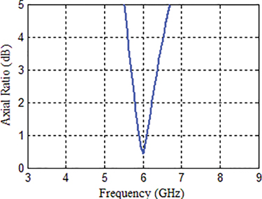
FIGURE 7.4 Variation of gain with frequency for truncated corner antenna.

FIGURE 7.5 Variation of axial ratio with frequency for truncated corner antenna.
7.3.2 Reconfigurable Circularly Polarized Microstrip Antennas
PIN diodes are used as a switch in several microstrip antennas. GaAs PIN diodes with a forward voltage of 0.73 V and forward current of 12 mA are used for switching the antenna. An antenna with three CP bands is developed, and the structure is shown in Figure 7.1b. It is achieved by embedding slits with unequal length at the boundary of the truncated rectangular radiating patch and making the PIN diodes ON and OFF. Figure 7.6 shows the simulated VSWR of the PIN diode-loaded antenna in OFF and ON conditions of the diode. When the diode is OFF, the antenna exhibits dual-band behaviour and the impedance bandwidth is in the frequency range from 4.48 to 6.77 GHz and from 7.46 to 8.28 GHz. The corresponding impedance bandwidth with OFF state of PIN diodes is 40.71% and 10.41%. When the diode is ON, the operating frequency is in the frequency range of 4.44–7.30 GHz and 8.06–8.77 GHz. The corresponding impedance bandwidth with ON state of PIN diodes is 48.72% and 8.43%.

FIGURE 7.6 Variation of VSWR with frequency for PIN diode- and horizontal slit-embedded truncated patch.
The variation of axial ratio with frequency is shown in Figure 7.7, and it is observed that for three frequency intervals, the axial ratio is below 3 dB, which indicates that the antenna can generate CP in three distinct bands. When the PIN diodes are OFF, they act as a simple notch in the antenna and split the single-band CP into double-band CP – one above and one below the original CP band. The two CP bands were obtained in the frequency range of 5–5.22 GHz and 6.49–6.71 GHz. The 3-dB AR bandwidth is 4.3% and 3.33%. It is seen that the centre frequency of CP operation is changed to 5.11 and 6.6 GHz from 6.025 GHz as in the antenna with truncated corners. The ON state of PIN diodes acts as an ohmic resistance and makes the gap connected and electric currents flow through the path. This effect of changed electric length of the surface current changes the resonant frequency of the two near-degenerate orthogonal modes, and the antenna gives CP at different frequencies. Figure 7.7 shows the axial ratio of a PIN diode-loaded antenna with horizontal slits also in the ON state of the diode. The 3-dB axial ratio bandwidth is 7.31% in the frequency range 5.40–5.81 GHz. It is seen from the figure that the antenna provides three CP bands by tuning the PIN diodes.

FIGURE 7.7 Axial ratio of PIN diode-loaded truncated corner antenna with horizontal slits.
Figure 7.8 shows the simulated gain of the antenna under both conditions of the diode. It is seen that gain drops in some frequency interval. The reduction in gain occurs in the frequency range where the radiation is not in phase and the phase difference decides the gain. The reduced gain in the last CP band indicates higher-order orthogonal modes combining to produce CP.

FIGURE 7.8 Gain of PIN diode-loaded truncated corner antenna with horizontal slits.
7.3.3 Impedance Bandwidth Improvement of Triple-Band CP Antennas
To increase the operational impedance bandwidth, an inclined slot was introduced, as shown in Figure 7.1c. The PIN diodes are intact at the gap between the two edges of the horizontal slits. When an inclined slot is cut inside the patch, there is a further increase in the length of the surface current path along the patch. The inclined slot and PIN diodes create two different resonances for the patch. The closeness among the resonances makes the broadband characteristics in the antenna. The broader bandwidth of the proposed antenna is due to the better control of current distribution towards the higher frequencies of the bandwidth that is achieved due to the inclined slot. Figure 7.9 shows the simulated and measured VSWR of the proposed antenna, and the simulated result shows a bandwidth of 66.61% ranging from 4.42 to 8.80 GHz with the ON state of PIN diodes, while Figure 7.10 shows the simulated and measured VSWR variations for the OFF state of the diode from 4.528 to 8.986 GHz, i.e. impedance bandwidth is 66.02%. In both the states of the diode, the proposed structure provides a better impedance bandwidth than a previous study [7]. The measured result shown for comparison is in good agreement with the simulated result. The mismatch between the measured and simulated results existed, which may be mainly caused by fabrication imperfection.
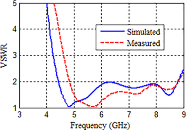
FIGURE 7.9 Measured and simulated VSWR for the proposed antenna with PIN diodes ON.
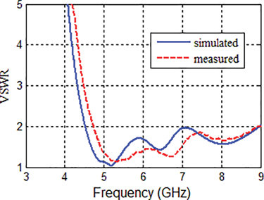
FIGURE 7.10 Measured and simulated VSWR for the proposed antenna with PIN diodes OFF.
Figure 7.11 shows the measured and simulated axial ratios of the proposed PIN diode-loaded antenna in the two states of the diode. It is clear from the figure that the antenna provides three circularly polarized bands by tuning the PIN diodes. The antenna exhibits CP in two bands with the frequency range from 4.88 to 5.07 GHz and from 6.51 to 6.71 GHz, when PIN diodes are OFF, i.e. the axial ratio bandwidth is 3.81% and 3.02%, respectively. With the ON state of the diodes, the antenna has another CP band from 5.31 to 5.61 GHz with the axial ratio bandwidth of 5.49%. The 3-dB axial ratio frequency range for all the three CP bands falls within the impedance bandwidth. Figure 7.12 depicts the measured and simulated gains with frequency for an inclined slot-loaded microstrip antenna with PIN diodes ON and OFF. It is clear from the graph that the gain is almost constant over the CP bands.
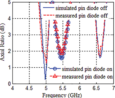
FIGURE 7.11 Measured and simulated axial ratios for the proposed antenna with PIN diodes ON and OFF.

FIGURE 7.12 Measured and simulated gains for the proposed antenna.
For the reception of the signal, it is important to find the direction of field rotation in terms of LHCP wave and RHCP wave. The simulated and measured LHCP and RHCP far-field distributions in the E-plane at the centre frequencies of individual CP bands 4.98, 5.46, and 6.60 GHz are shown in Figure 7.13a–c, respectively. From these figures, it is clear that the antenna is LHCP with a considerable axial ratio beam width. A good amount of cross-polarization attenuation is obtained at all centre frequencies.
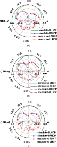
FIGURE 7.13 Simulated and measured LHCP and RHCP patterns at (a) 4.98GHz, (b) 5.46 GHz, and (c) 6.60 GHz.
Figure 7.14a and b shows the current distribution on the radiating patch for different time frames: t = 0(0°), t = T/4(90°), t = 2T/4(180°), and t = 3T/4(270°) at the centre frequencies of CP bands with PIN diodes OFF, while Figure 7.15 shows the same at the centre frequencies of CP band with PIN diodes ON. The surface current distribution on the radiating patch at the time frames clearly indicates the circularly polarized field radiation. The field rotates in the clockwise direction, which results in exciting a LHCP radiation.

FIGURE 7.14 Surface current distribution for the proposed antenna with PIN diodes OFF at (a) 4.98 GHz and (b) 6.60 GHz.

FIGURE 7.15 Surface current distribution for the proposed antenna with PIN diodes ON at 5.46 GHz.
7.3.4 Parametric Study of Quad-band CP Antennas
The effects of dimensions of the slits, slot, and corner truncation on the reflection coefficient and axial ratio of the proposed antenna are investigated. In the investigation, one parameter is varied at a time, while others are kept constant. The effects of these geometrical parameters mentioned above on the reflection coefficient are very small and are not considered. Figure 7.16 shows the axial ratio for the change in the length of slit L1. It can be noticed that with decreasing slit length L1, CP band AR5 disappears and only three CP bands are obtained. Four CP bands are obtained with an increase in the slit length L1. The effect of change in slit length L2 is shown in Figure 7.17. With the decrease and increase in the slit length L2, three and two CP bands are obtained, respectively. A significant effect is observed on CP bands AR5 and AR4 which disappeared with the increase in the slit length, and CP band AR5 disappears when the slit length decreased.

FIGURE 7.16 Variation of axial ratio for different values of slit’s length L1 in the upper patch.
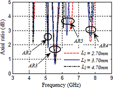
FIGURE 7.17 Variation of axial ratio for different values of slit’s length L2 in the upper patch.
Figure 7.18 shows the axial ratio for the change in the length of slit L3. It can be seen that as the L3 decreases, CP bands AR2 and AR4 disappear and only two CP bands are obtained, while three CP bands are obtained with increasing L3. Figure 7.19 illustrates that with decreasing slot length L4, CP bands AR2 and AR5 disappear, while four CP bands are obtained with increasing slot length L4. Figure 7.20 shows the axial ratio for the change in the length of corner truncation. It can be clearly seen that CP bands strongly depend on the truncation length ∆L. Only two CP bands are obtained with increasing and decreasing truncation length ∆L. The CP bands AR5 and AR4 disappear with decreasing truncation length, while CP bands AR2 and AR4 disappear with increasing truncation length. The effects on the centre frequencies (CF) and the axial ratio bandwidth (ARBW) of the different CP bands of the antenna with variation in the length of slits, slot, and corner truncation are summarized in Table 7.3. With decreasing slit length L1, the CF of the CP bands AR2, AR3, and AR4 shifted slightly upwards, while the ARBW of CP bands AR2 and AR4 decreased and the ARBW of CP band AR3 increased. With an increase in the slit length L1, the CF of all CP bands shifted downwards. The ARBW of CP bands AR2, AR4, and AR5 increased, while the ARBW of CP band AR3 decreased. With increasing and decreasing slit length L2, a small effect is observed on the CF and ARBW of CP bands. The CF of the CP bands AR3 and AR5 shifted upwards with a small increase in the ARBW by decreasing the slit length L3, while the CF of CP bands AR2, AR3, and AR4 shifted slightly downwards with a small change in the ARBW by increasing the slit length L3. A small change is observed on the CF and ARBW of the CP bands with the increase and decrease in the slot length L4. From the table, it is also observed that the CF of CP bands AR2 and AR3 shifted downwards, while the ARBW of CP bands AR2 and AR3 decreased and increased, respectively, upon decreasing the corner truncation length ∆L. The CF of CP bands shifted upwards with increased ARBW upon increasing the corner truncation length ∆L.

FIGURE 7.18 Variation of axial ratio for different values of slit’s length L3 in the lower patch.
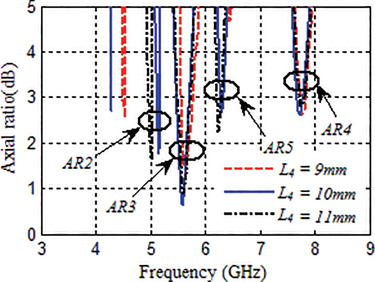
FIGURE 7.19 Variation of axial ratio for different values of slot’s length L4 in the lower patch.
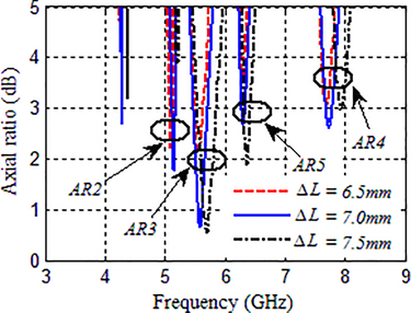
FIGURE 7.20 Variation of axial ratio for different values of corner truncation’s length ∆L.
|
|
AR2 |
AR3 |
AR5 |
AR4 |
|||||||
|---|---|---|---|---|---|---|---|---|---|---|---|---|
Parameter |
Value (mm) |
CF (GHz) |
|
ARBW (%) |
CF (GHz) |
ARBW (%) |
CF (GHz) |
|
ARBW (%) |
CF (GHz) |
|
ARBW (%) |
L1 |
5.75 |
5.158 |
|
0.33 |
5.6843 |
5.840 |
|
NA |
|
7.7703 |
|
0.90 |
|
6.75 |
5.1476 |
|
0.98 |
5.5905 |
4.275 |
6.3026 |
|
0.8869 |
7.7298 |
|
1.35 |
|
7.75 |
5.1213 |
|
1.13 |
5.522 |
2.72 |
6.147 |
|
2.28 |
7.7273 |
|
1.37 |
L2 |
2.70 |
5.1459 |
|
0.88 |
5.6079 |
4.37 |
|
NA |
|
7.7431 |
|
2.13 |
|
3.70 |
5.1476 |
|
0.98 |
5.5905 |
4.275 |
6.3026 |
|
0.8869 |
7.7298 |
|
1.35 |
|
4.70 |
5.151 |
|
1.12 |
5.6091 |
4.57 |
|
NA |
|
|
NA |
|
L3 |
4.0 |
|
NA |
|
5.7036 |
4.71 |
6.3336 |
|
1.53 |
|
NA |
|
|
5.0 |
5.1476 |
|
0.98 |
5.5905 |
4.275 |
6.3026 |
|
0.8869 |
7.7298 |
|
1.35 |
|
6.0 |
5.1356 |
|
1.49 |
5.5078 |
3.73 |
|
NA |
|
7.3359 |
|
2.29 |
L4 |
9.0 |
|
NA |
|
5.6589 |
3.77 |
|
NA |
|
7.7727 |
|
1.304 |
|
10.0 |
5.1476 |
|
0.98 |
5.5905 |
4.275 |
6.3026 |
|
0.8869 |
7.7298 |
|
1.35 |
|
11.0 |
4.9920 |
|
1.15 |
5.6037 |
4.08 |
6.2488 |
|
1.44 |
7.7579 |
|
1.10 |
ΔL |
6.0 |
5.1023 |
|
1.08 |
5.5587 |
2.64 |
|
NA |
|
|
NA |
|
|
7.0 |
5.1476 |
|
0.98 |
5.5905 |
4.275 |
6.3026 |
|
0.8869 |
7.7298 |
|
1.35 |
|
8.0 |
|
NA |
|
5.6934 |
5.52 |
6.3676 |
|
1.52 |
|
NA |
|
By parametric studies mentioned above, the design procedure for a quad-band CP antenna is obtained and it is observed that the lengths of slits, slot, and corner truncation are the critical parameters and play an important role in generating quad-band CP operation.
7.3.5 Simulated and Measured Results
The reflection coefficient and axial ratio of a slit-loaded truncated patch before stacking are shown in Figure 7.21. The impedance bandwidth of 37.83% in the frequency range of 4.65–6.82 GHz is achieved for the slit-loaded truncated patch. By properly tuning the dimensions of the slits, the antenna produces two CP bands in the frequency range 5.0–5.22 GHz and 6.49–6.71 GHz, as shown in Figure 7.21, and the 3-dB axial ratio bandwidth of 4.31% and 3.34%, respectively. Now, another rectangle patch of dimensions L × W is etched on the bottom surface of the substrate with the centre of two patches aligned and a pair of the opposite corners of the bottom patch is also removed. The truncation dimension is the same as for upper patch. But by this process, the antenna is converted to single-band CP from dual-band CP. So, to achieve the multiband CP operation again, a horizontal slit on the bottom patch is introduced, as shown in Figure 7.2c. As a result, triple-band CP radiation is achieved. Figure 7.8 shows the reflection coefficient and axial ratio of a slit-loaded stacked patch. The antenna shows dual-band response in the frequency range 4.33–6.13 GHz and 6.54–7.37 GHz with an impedance bandwidth of 34.41% and 11.93%, respectively. The corresponding CP bands of the said antenna are also characterized from Figure 7.22. From the figure, it is clear that the first three CP bands, i.e. AR1, AR2, and AR3, which are achieved by selecting the proper dimensions of the slit into the bottom patch, fall within the first band of operation. The 3-dB axial ratio bandwidths are 0.864%, 2.37%, and 3.24% in the frequency range 4.5959–4.6358 GHz (AR1), 5.5126–5.6453Ghz (AR2), and 5.8471–6.0397 GHz (AR3), respectively. It is important to note that the 3-dB axial ratio bandwidth should fall within the impedance bandwidth for the proper operation of the circularly polarized microstrip antenna. It is also seen from Figure 7.22 that there is another CP band in the frequency range 7.7467–7.9017 GHz (AR4), which does not lie within the impedance bandwidth. Now, the aim here is to match the antenna impedance to cover CP band AR4. For this, a slot is embedded in the centre of the bottom patch along the diagonal axis and the feed location (d) is optimized at 2.13 mm. Figure 7.23 shows the simulated reflection coefficient and axial ratio at 200 from broadside. This proposed antenna covers the frequency band of 4.97–8.49 GHz with an impedance bandwidth of 55.6%. In this process, the lower CP band AR1 is detuned, but the old CP band AR4 falls in the band of operation and a new CP band AR5 is introduced in the band and the antenna shows quad-band CP operation. It is clear from the figure that four distinct CP bands fall within the operating band and at each CP band, the axial ratio is below 3 dB, which means that the antenna has a good CP performance. The 3-dB axial ratio bandwidths are 0.98%, 4.275%, 0.8869%, and 1.35% in the frequency band 5.1223–5.1729 GHz (AR2), 5.4710–5.7100 GHz (AR3), 6.2747–6.3306 GHz (AR5), and 7.6775–7.7822 GHz (AR4), respectively. The figure also shows the measured reflection coefficient of the proposed antenna. The measured result is in close agreement with the simulated result. Figure 7.24 illustrates the simulated and measured axial ratios of the proposed antenna for the CP bands AR2 and AR3. The simulated and measured axial ratios for the CP bands AR5 and AR4 are shown in Figure 7.25. However, to perform the axial ratio measurement in an anechoic chamber, the antenna under test (AUT) is referred to as source. Then, a linearly polarized antenna, usually a horn antenna, is used as the receiver antenna. A linearly polarized receiver antenna is rotated in the plane of polarization from 0° to 360°. The minimum and maximum values of power received at the given frequency are recorded. The difference between the minimum and maximum values of power was considered as the axial ratio at that frequency. This measurement process was repeated for all the frequency points, and the graph was plotted. The measured and simulated gains at 200 from the broadside are presented in Figure 7.26. For the CP bands AR2, AR3, AR5, and AR4, the antenna gain varies from 4.03 to 2.8624 dBic, 6.07 to 5.8743 dBic, 5.29 to 5.40 dBic, and 7.67 to 4.66 dBic, respectively. The gain of the antenna was measured at far-field using the substitution method in an anechoic chamber. Two calibrated horn antennas of known gain as the transmitter antenna are used to find the unknown gain of AUT. The AUT as the receiver antenna was placed on the positioner with required elevation and azimuthal coverage. The AUT was then replaced with the second horn antenna of calibrated gain, and similar measurement was repeated. Difference between the measured powers reflects the gain difference between the two receiving antennas, and the absolute gain of the AUT is calculated. The whole measurement procedure was repeated by changing the distance between the transmitter and receiver antennas using the positioner movement, and the average gain was considered as the final gain value. The measured and simulated left-hand circular polarization (LHCP) and right-hand circular polarization (RHCP) radiation patterns in xoz plane at centre frequencies of CP bands AR2, AR3, AR5, and AR4 are presented in Figure 7.27a–d, respectively. It is observed that the LHCP is radiated for all the CP bands, and the maximum radiation is achieved at 20° from broadside. However, the squinting of the main beam can be improved to radiate at boresight by making an array of the antenna, properly setting the spacing between the antennas and adjusting the feed angle to the antenna.

FIGURE 7.21 Reflection coefficient and axial ratio of the slit-loaded truncated patch without stacking with d = 0.5 mm [solid graph shows reflection coefficient and dotted graph shows axial ratio].

FIGURE 7.22 Reflection coefficient and axial ratio of the slit-loaded stacked truncated patch with d = 0.5 mm [solid graph shows reflection coefficient and dotted graph shows axial ratio].

FIGURE 7.23 Reflection coefficient and axial ratio of the proposed antenna simulated reflection coefficient measured reflection coefficient axial ratio [the solid line shows simulated reflection coefficient, -. line shows measured reflection coefficient and .. line shows axial ratio].

FIGURE 7.24 Simulated and measured axial ratios of the proposed antenna for CP bands AR2 and AR3.

FIGURE 7.25 Simulated and measured axial ratios of the proposed antenna for CP bands AR5 and AR4.

FIGURE 7.26 Simulated and measured gains of the proposed antenna.
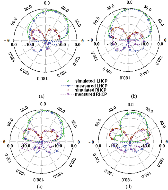
FIGURE 7.27 Simulated and measured radiation patterns of the proposed antenna in xoz plane: (a) at 5.14 GHz, (b) at 5.59 GHz, (c) at 6.30 GHz, and (d) at 7.729 GHz.
7.3.6 Operating Mechanism
The operating mechanism of the antenna in the four bands of the CP operation can be explained with the help of current distribution at the two patches of the antenna. Various geometrical parameters play their role in generating different CP bands. Figure 7.28a–d shows the electric current distribution at the centre frequencies of the different CP bands for the upper patch (UP) and lower patch (LP) at four different time instants, that is, at ωt = 0°, 90°, 180°, and 270°, respectively, where ω is the angular frequency and t is time. In the explanation, the path difference due to inter patch spacing is neglected. At the centre frequency of the first CP band, i.e. 5.14 GHz, the inclined slot and corner truncation are responsible for CP generation. At feed angle ωt = 0°, the current vector at UP is oriented at an angle of 135°. At ωt = 90°, the electric currents from the truncated corners of the LP and UP are cancelled, resulting in the radiation from the inclined slot only, which is at an angle of 45°. At ωt = 180° and 270°, the reverse radiation happens to those at ωt = 0° and ωt = 90°, and the resulting radiation takes place at an angle of 315° and 225°, respectively. Hence, the E-field vector rotates clockwise as time increases, thus producing the LHCP radiation. At the centre frequency of the second CP band, i.e. 5.59 GHz, the radiation from both patches determines the direction of the resultant electric field. At ωt = 0°, the resultant two vector currents make the radiation at 157.5°, while at ωt = 90°, these vector currents fall at 0° and 135°, resulting in the radiation at 67.5°. Similarly, the resultant vector at ωt = 180° and ωt = 270° radiates at 337.5° and 247.5°, respectively. Hence, again, these radiation directions indicate a LHCP pattern. At the centre frequency of the third CP band, i.e. 6.30 GHz, the slit length L1 plays an important role. The current vectors due to the truncated corners are opposite to each other cancelling the radiation. Hence, at ωt = 0°, the resultant E-field vector is at an angle 180°. At ωt = 90°, the horizontal E-field from LP and UP are cancelled out, resulting in only vertical E-field (90°) from the two patches. Similarly, at ωt = 180° and ωt = 270°, the resulting radiation becomes at 0° and 270°, respectively, suggesting a LHCP radiation again. At the centre frequency of the fourth CP band, i.e. 7.729 GHz, the slit’s lengths L1 and L2 on the UP are responsible for CP radiation. All the E-field vectors except vertically downward vectors at the edge of lower slit are cancelled out, and the resultant radiation occurs at an angle of 270° for ωt = 0°. At ωt = 90°, the upper slit radiates at 180° dominating other E-field vectors. Similarly, at ωt = 180° and ωt = 270°, the resultant E-field vectors radiate at 90° and 0°, respectively, rotating the field clockwise indicating a LHCP radiation.
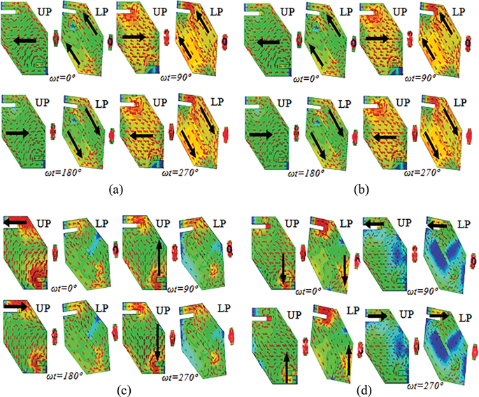
FIGURE 7.28 Simulated current densities of the proposed antenna at centre frequencies of circularly polarized bands: (a) at 5.14 GHz, (b) at 5.59 GHz, (c) at 6.30 GHz, and (d) at 7.729 GHz.
7.4 Conclusion
In this chapter, two antennas of three and four CP bands were discussed. The first antenna operated in three CP bands using PIN diodes, while the second antenna used stacking to achieve this. Both antennas were corner-truncated and suspended in air. Two horizontal slits of unequal lengths with PIN diodes on the truncated patch were cut to achieve the goal. Triple-band circular polarization was realized by switching PIN diodes across the slits ON and OFF. The broadband performance of the proposed antenna was realized by embedding an inclined slot on the patch with PIN diodes across the horizontal slits. The impedance bandwidth of the antenna increased from 51% to 66.61% (ON state) and 66.02% (OFF state) as compared to the capacitive-coupled probe-fed microstrip antenna reported earlier, and three distinct LHCP bands were also generated. An axial ratio bandwidth for the proposed antenna of 3.81%, 3.02%, and 5.49% was realized. A good LHCP performance was achieved in the three bands with respect to cross-polarization attenuation and axial ratio beam width. The results of the proposed antenna show that it is very suitable for various wireless communication system applications. The proposed antenna is useful for 5 GHz WLAN and may be used for public safety WLAN (IEEE802.11y) at 4.9 GHz, IEEE 802.11ac Wi-Fi at 5 GHz, which has the expected WLAN throughput of at least 1 GB/s and was approved in January 2014, and HIPERLAN/2(5.470–5.725 GHz).
Apart from this, the quad-band circularly polarized capacitive-coupled stacked patch antenna with wideband characteristics for C-band applications can be used as a multiband device for CP applications. Only two stacked patches were used to achieve quad-band CP operation. The antenna gave an impedance bandwidth of 55.46% and showed quad-band CP performance with axial ratio bandwidths of 0.98%, 4.275%, 0.8869%, and 1.35%. Good LHCP patterns were achieved in all the four distinct CP bands. The CP band AR2 in the frequency band 5.1223–5.1729 GHz covers HIPERLAN/1 and fixed satellite services (earth to space) (5.091–5.15 GHz). The CP band AR3 in the frequency range 5.4710–5.7100 GHz can be used for HIPERLAN/2 and amateur satellite uplink (5.650–5.670 GHz). The CP band AR5 in the frequency band 6.2747–6.3306 GHz can be used for C-band communication satellites for their uplinks (5.925–6.425 GHz).
References
1. Garg, R.; Bhartia, P.; Bahl, I.; and Ittipiboon, A.: Microstrip Antenna Design Handbook. Artech House, Norwood, MA, (2001).
2. Schaubert, D.H.; Pozar, D.M.; and Adrian, A.: Effects of microstrip antenna substrate thickness and permittivity: comparision of theories and experiment. IEEE Transactions Antennas Propagation, 37(1989), 677–682.
3. Pues, H.F.; and Van De Capelle, A.R.: An impedance matching technique for increasing the bandwidth of microstrip antenna. IEEE Antennas and Propagation Magazine, 37–11(1989), 1345–1354.
4. Weigand, S.; Huff, G.H.; Pan, K.H.; and Bernhard, J.T.: Analysis and design of broadband single layer rectangular U-slot microstrip patch antenna. IEEE Transaction on Antennas and Propagation, 51–3(2033), 457–468.
5. Deshmukh, A.A.; and Kumar, G.: Broadband and compact V-slot loaded RMSAs. Electron Letters, 42–17(2006), 951–952.
6. Targonski, S.D.; Waterhouse, R.B.; and Pozar, D.M.: Wideband Aperture coupled Stacked patch antenna using thick substrate. Electron Letters, 32–21(1996), 1941–1942.
7. Kasabegoudar, V.G.; and Vinoy, K.J.: Coplanar capacitively coupled probe fed microstrip antenna for wideband applications. IEEE Transaction on Antennas and Propagation, 58–10(2010), 3131–3138.
8. Chang, F.S.; Wong, K.L.; and Chion, T.W.: Low cost broadband circularly polarized patch antenna. IEEE Transaction on Antennas and Propagation, 51(2003), 3006–3009.
9. Sharma, P.C.; and Gupta, K.P.: Analysis and optimized design of single feed circularly polarized microstrip antenna. IEEE Transaction on Antennas and Propagation, 29(1983), 949–955.
10. Wong, K.-L.; and Wu, J.-Y.: Single feed Small circularly polarized square microstrip antenna. Electron Letters, 33–22(1997), 1833–1834.
11. Chen, W.-S.; Wu, C.-K.; and Wong, K.-L.: Novel compact circularly polarized square microstrip antenna. IEEE Transaction on Antennas and Propagation, 49–3(2001), 340–342.
12. Wong, K.-L.; and Lin, Y.-F.: Circularly polarized microstrip antenna with a tuning stub. Electron Letters, 34–9(1998), 831–832.
13. Iwasaki, H.: A circularly polarized small-sized microstrip antenna with a cross-slot. IEEE Transactions on Antennas Propagation, 44–10(1996), 1399–1401.
14. Pozar, D.M.; and Duffy, S.M.: A dual band circularly polarized aperture coupled stacked microstrip antenna for global positioning satellite. IEEE Transactions on Antennas Propagation, 45–11(1997), 1618–1625.
15. Yu, A.; Yang, F.; and Elsherbeni, A.: A dual band circularly polarized ring antenna based on composite right and left handed metamaterials. Progress in Electromagnetics Research, 78(2008), 73–81.
16. Fujimoto, T.; Ayukawa, D.; Iwanaga, K.; and Taguchi, M.: Dual band circularly polarized microstrip antenna for GPS application. IEEE Antenna Propagation Society International Symposium, S (2008), 1–4.
17. Heidari, A.A.; Heyrani, M.; and Nakhkash, M.: A dual band circularly polarized stub loaded microstrip patch antenna for GPS applications. Progress in Electromagnetics Research, 92(2009), 195–208.
18. Chen, R.-H.; and Row, J.-S.: Single fed microstrip patch antenna with switchable polarization. IEEE Transactions on Antennas Propagation, 56–4(2008), 922–926.
19. Zhou, Y.; Chen, C.-C.; and Volkis, J.L.: Dual band proximity fed stacked patch antenna for tri-band GPS applications. IEEE Transactions on Antennas Propagation, 55–1(2007), 220–223.
20. Doust, E.G.; Clenet, M.; Hemmati, V.; and Wight, J.: An aperture coupled circularly polarized stacked microstrip antenna for GPS frequency bands L1, L2, L5. IEEE Transactions Antennas and Propagation Society International Symposium, (2008), 1–4.
21. Falade, O.P.; Rehman, M.U.; Gao, Y.; Chen, X.D.; and Parini, C.G.: Singe feed stacked circular polarized antenna for triple band operation. IEEE Transactions on Antennas Propagation, 60–10(2012), 4479–4484.
22. Lio, W.; Chu, Q.X.; and Du, S.: Triple band circularly polarized stacked microstrip antenna for GPS and CNSS applications. In ICMMT Proceeding, (2010), 252–255.
23. Yim, H.-Y.A.; Kong, C.-P.; and Cheng, K.-K.M.: Compact circularly polarized Microstrip antenna design for dual band applications. Electron Letters, 47–7(March 2006), 380–381.
24. Zhang, Y.-Q.; Li, X.; Yang, L.; and Gong, S.-X.: Dual band circularly polarized annular –ring microstrip antenna for GNSS application. IEEE Transactions and Wireless Propagation Letters, 12(2013), 615–618.
25. Lee, H.R.; Ryu, H.K.; Lim, S.; and Woo, J.M.: A miniaturized, dual – band, circularly polarized microstrip antenna for installation into satellite mobile phones. IEEE Transactions and Wireless Propagation Letters, 8(2009), 823–825.
26. Yuan, H.Y.; Zhang, J.Q.; Qu, S.B.; Zhou, H.; Wang, J.F.; Ma, H.; and Xu, Z.: Dual band dual polarized microstrip antenna for compass navigation satellite system. Progress in Electromagnetics Research, 30(2012), 213–223.
27. Yang, K.P.; and Wong, K.-L.: Dual –band circularly polarized square microstrip antenna. IEEE Transactions on Antennas and Propagation, 49(2001), 377–382.
28. Lai, X.-Z.; Xie, Z.-M.; and Cen, X.-L.: Design of dual circularly polarized antenna with high isolation for RFID applications. Progress in Electromagnetics Research, 139(2013), 25–39.
29. Yuan, H.Y.; Zhang, J.Q.; Qu, S.B.; Zhou, H.; Wang, J.F.; Ma, H.; and Xu, Z.: Dual band dual polarized microstrip antenna for compass navigation satellites system. Progress in Electromagnetics Research, 30(2012), 213–223.
30. Eselle, K.P.; and Verma, A.K.: Wideband circularly-polarized stacked microstrip antennas. IEEE Antennas and Wireless Propagation Letters, 6(2007), 21–24.
31. Rama Rao, B.; Smolinski, M.A.; Quach, C.C.; and Rosario, E.N.: Triple band GPS trap – loaded inverted L antenna array. Microwave and Optical Technology Letters, 38–1(July 2003), 35–37.
32. Falade, O.P.; Chen, X.; Alfadhi, Y.; and Parini, C.: Quad band circular polarised antenna. Antenna and Propagation Conference(LAPC), Loughborough, (2012), 1–4.
33. Kumar, G.; and Ray, K.P.: Broadband Microstrip Antennas. Artech House, Boston, London, (2003).
34. Singh, D.K.; Kanaujia, B.K.; Dwari, S.; Pandey, G.P.; and Kumar, S.: Reconfigurable circularly polarized capacitive coupled microstrip antenna. International Journal of Microwave and Wireless Technologies, 9–4(May 2017), 843–850.
35. Singh, D.K.; Kanaujia, B.K.; Dwari, S.; Pandey, G.P.; Kumar, S.: Novel quad‐band circularly polarized capacitive‐fed microstrip antenna for C‐band applications. Microwave and Optical Technology Letters, 57–11(2015), 2622–2628.