
12
On-Chip AER Communication Circuits

This chapter covers the on-chip transistor circuits used for the communication fabric introduced in Chapter 2; in particular the asynchronous communication circuits for receiving and transmitting address events following the Address Event Representation (AER) protocol. AER circuits are needed for transmitters that emit address events, for example the sensors described in Chapters 3 and 4 and the multineuron chips in Chapter 7. The receivers decode the incoming address events and stimulate the corresponding synapses and neurons on multineuron circuits as described in Chapters 7 and 8. They can also be stimulated by outputs of commodity digital chips or artificial spike trains played from the computer via interfaces of the kind described in Chapter 13.
12.1 Introduction
The circuits for the early neuromorphic chips were first designed by Sivilotti (1991) and Mahowald (1994), students at the time in Carver Mead’s laboratory at Caltech. These designs were influenced by the then on-going research in design of asynchronous circuits within the groups of Chuck Seitz and Alain Martin at Caltech. Designing asynchronous circuits was no easy matter at the time because design tools for asynchronous circuits were nonexistent. The Communicating Hardware Processes (CHP) design methodology introduced by Alain Martin, helped to facilitate the design of general asynchronous circuits (Martin 1986; Martin and Nyström 2006). This methodology involves the application of a series of program decompositions and transformations starting from a high-level specification of the intended system. As each step preserves the logic of the original program, the resulting circuit will be a correct logical implementation of the specifications. This methodology was used in Martin’s laboratory to design various custom asynchronous processors including field-programmable gate arrays (FPGAs) and microcontrollers (Martin 1986; Martin et al. 1989, 2003).
Using this methodology, the on-chip AER circuits necessary on a transmitter (sender) for communicating address events asynchronously off-chip to a receiver have been constructed. Detailed information on how the AER transistor blocks are constructed following the CHP design methodology can be found in Boahen (2000, 2004a, 2004b, 2004c).
12.1.1 Communication Cycle
The block diagram in Figure 12.1 shows the organization of the various AER blocks within two-dimensionally organized transmitter and receiver chips. Signal flow between any two communicating blocks is carried out through the Request (R) and Acknowledge (A) signals. The initiation of a spike from a pixel in the transmitter starts a communication cycle first between the pixel and a block known as the row arbiter. The pixel does this by activating the row request RR line to the Y-arbiter. Any active pixel on this row will also activate the same RR line. The Y-arbiter block arbitrates among multiple active row requests and acknowledges only one of these requests by activating the corresponding RA row line. (Details of the arbitration process and circuits follow in Section 12.2.2.) The pixels on the row with an active RA signal then request in the column direction by activating their corresponding CR line to the X-arbiter. The X-arbiter then acknowledges one of these column requests through the corresponding CA line. The X- and Y-arbiters also communicate with the X- and Y- encoders, which code the selected row and column addresses of the selected pixel. They also start a communication cycle with an on-chip handshaking logic block which handles the communication off-chip through CXREQ and CXACK. On receiving both the activated RA and CA lines, the pixel will then withdraw its request (i.e., it will no longer pull on these lines) from both arbiters. The Y-arbiter does not start the next handshaking cycle with the remaining active row requests until the off-chip handshaking cycle is completed.

Figure 12.1 Block diagram of AER blocks on a 2D transmitter chip and 2D receiver chip. Details of signaling are described in the text. The signals CXREQ and CXACK can be connected to CRREQ and CRACK, if no translation of addresses from the transmitter are needed
The off-chip communication cycle occurs between the transmitter and the receiver. The communication path in this case consists of both a data path (the digital address of the active pixel) and a control path (the request and acknowledge signals of the two devices). Following the single-sender, single-receiver signaling protocol in Figure 2.14, the data should be valid before the chip request R is activated. This sequence means that R can only be activated by the sender after a small delay from the onset of changing the address bits which encode the spike address to be transmitted. This protocol is also known as the bundled data protocol and is not truly delay insensitive as is required of standard asynchronous circuits. The delay-insensitive property is important in the circuit construction to ensure proper operation regardless of the final delay through the wires and transistors of asynchronous circuits in the fabricated device.
Most neuromorphic chips use the bundled data protocol because the circuits to generate the chip request signal are more compact than the delay-insensitive version. The delay in generating the chip request signal is usually done through a set of current-starved inverters and capacitors and this delay will vary after fabrication. The circuits have to be designed so that this delay variation is as small as possible for all process corners. The delay-insensitive version uses a dual-rail encoding scheme where each address bit is represented by two lines. One of the two lines is activated when transmitting a ‘0’ and the other line is activated when transmitting a ‘1’. A completion circuit then determines when one of the two lines for every address bit has been activated (Martin and Nyström 2006). The output of the completion circuit acts as the chip request signal. The trade-off between the bundled data protocol and the delay-insensitive version is that the dual-rail encoding scheme needs twice as many output pads and the additional completion circuits for generating the chip request signal.
The receiver on receiving an active CRREQ generates an active CRACK signal which is also used to latch the input digital address. The decoded X- and Y-addresses are then used to stimulate the corresponding pixel through activated row and column lines. When CRREQ is inactivated by the transmitter, CRACK is inactivated once the acknowledge signal of the pixel array (summed from all pixel acknowledges) is active, signaling that the pixel has received the decoded address. In some chips, the design is such that the pixel acknowledge is not used for the inactivation of the CRACK as a way of speeding up the communication cycle. This timing assumption is valid only if the on-chip decoding process is faster than the duration of the off-chip communication.
12.1.2 Speedup in Communication
The control flow of the request and acknowledge signals from a pixel on a transmitter to a pixel on a receiver is illustrated in Figure 12.2. In this diagram, the four-phase handshaking protocol shown in Figure 2.14 is assumed. When the Set phase of the pixel is initiated starting with the activation of the request from this pixel to the encoder and arbiter, this information is propagated all the way to a pixel on the receiver. The receiver pixel then activates its acknowledge signal, and this acknowledge information is transmitted all the way back to the pixel on the transmitter. When this cycle is completed, the Reset phase is executed starting from the inactivation of the request from the transmitter pixel all the way to the pixel on the receiver, whereupon the acknowledge signal from this pixel is now inactivated leading to the propagation of the inactivation of the acknowledge to the pixel on the transmitter. The communication time can be extremely long, since the request originating from a pixel on the transmitter has to be communicated all the way to a pixel on the receiver before the acknowledge from the encoder to the transmitter pixel can be activated. To speed up this communication cycle, pipelining is implemented where the Set phase is completed locally between two communicating processes without waiting for the activation of the request signal from a pixel on the sender to propagate all the way to the pixel on the receiver (Sutherland 1989). We return to this issue in Section 12.2.2.

Figure 12.2 Control signal flow starting from a pixel through the arbiter and encoder on a transmitter to the decoder and a pixel on the receiver (left to right). The arrows show the activation of the requests between the various blocks (from left to right) and activation of the corresponding acknowledges (from right to left) in the Set phase and then first the inactivation of the request and the inactivation of the acknowledge signals in the Reset phase. (a) Completion of the set phase for the originating pixel before the handshaking is completed in the reset phase. (b) Pipelining reduces the overall handshaking time by allowing the signals to propagate forward in the set phase without waiting for the reset phase of the previous stage. SPpixel, the set phase of the pixel is shorter in duration than the set phase in (a). © 2000 IEEE. Reprinted, with permission, from Boahen (2000)

Figure 12.3 Muller C-element. (a) Transistor circuits. The feedback inverters hold the state c′ when both inputs a and b do not have the same logic input state. (b) Truth table of this circuit means previous state. (c) Symbol for C-element gate. (d) Symbol for an asymmetric C-element gate in which the pFET M1 is not present in the transistor circuit shown in (a)
12.2 AER Transmitter Blocks
The three main types of handshaking blocks on a transmitter consist of the handshaking circuits within the pixel, the arbiter, and a chip-level handshaking logic block. The activation of signals in the handshaking protocol between two communicating processes is implemented through the Muller C-element gate shown in Figure 12.3a (Muller and Bartky 1959). The a and b inputs are driven by the request R and acknowledge A signals of a process. The output c does not change unless both a and b inputs are at 0 or 1. Because the output is not always driven, a staticizer consisting of two inverters connected in feedback holds the output state c’ until a and b are at the same logic level. The truth table of this gate and its symbol is given in Figure 12.3b and 12.3c, respectively. If one of the pFETs or nFETs is removed, the circuit is known as an asymmetric C-element. In the case where the pFET M1 is removed as in (a), only the b input has both its up-going and down-going transitions checked and the corresponding symbol for this circuit is shown in (d). The asymmetric C-element is used in the fair arbiter circuit described in Section 12.2.2.
12.2.1 AER Circuits within a Pixel
The AER communication circuitry is frequently implemented through a neuron-like circuit, for example the Axon-Hillock circuit, but can be implemented by any circuit that generates digital pulses. In the Axon-Hillock circuit (see Figure 12.4), the input current Iin generated by the actual intended circuits for the function of the pixel, charges up a neuron-like circuit. The example in the figure assumes that Iin is generated by a synapse circuit. This current then charges up the membrane capacitance C1. When the membrane voltage Vm exceeds the threshold of the first inverter, the output of the second inverter, Vsp, becomes active and Vm is further increased by the positive feedback through C1 and C2. Vsp drives M1 to pull down on nRR. When the RA line is activated from the row arbiter, transistors M2 and M3 activate nCR. When the CA line is activated by the column arbiter, Vm is pulled low, thus resetting the neuron output Vsp, which in return stops pulling down nRR. This row line has a pullup (shown in Figure 12.11b) which returns nRR to Vdd when no pixel is requesting. This method is called a wired OR which replaces a conventional OR gate and reduces considerably the area required by replacing all the pull-up transistors with a single pFET. This pFET can be either connected to a fixed voltage (passive) or is actively driven by a peripheral handshaking circuit. The active-driven p-channel FET (pFET) scheme is described in Section 12.3.5.

Figure 12.4 Example AER handshaking circuits within a neuron pixel. The neuron is modeled by the Axon-Hillock circuit. The handshaking signals generated by the circuit are the row request and acknowledge signals, nRR and RA, and the column request and acknowledge signals, nCR and CA, respectively. The prefix “n”on a signal name means that the signal is active low. Details of the circuit operation are described in the text
12.2.2 Arbiter1
The arbiter receives the row or column request lines from the pixel array through the arbiter interface block and arbitrates amongst the active lines (see Figure 12.5). The arbiter interface block handles the handshaking signals from the row (or column) requests and acknowledges and the ChipAck signal. It is discussed further in Section 12.2.3. For each dimension of row and column (assuming N rows or columns), the arbiter consists of a tree-like structure of N − 1 two-input arbiter cells, arranged in a tree with b = log2(N) levels required to arbitrate between N pixels. Each two-input arbiter gate outputs a Req to the two-input arbiter at the next level, if any one of its two input Req signals is active. For example, the input request signals are labelled as r11 and r12 for the two-input gate A1 and the corresponding Ack lines are a11 and a12. The output signal r21 from A1 goes to one of the two inputs of the next arbiter gate B1. This process continues to the top of the tree. The final selected output Req at the top of the tree then goes to an inverter, and the inverted output becomes the Ack signal that now propagates downward through the various gates until the corresponding RA line of an active RR line of a row of an array is activated by the arbiter interface block. For a 2D array, a second arbiter handles the CR and CA lines from the active pixels of the acknowledged row in the column dimension.

Figure 12.5 Communication interface between pixels of different rows and the arbiter tree of two-input arbiter gates. The circuits of the arbiter interface block are shown in Figure 12.11. The arbiter arbitrates amongst the nRR lines from the active rows in the array. In this figure, we assume that each row consists only of a single pixel
Arbiter circuits are designed to satisfy two criteria: low latencies and fairness. The first criteria ensures that incoming requests will be serviced as quickly as possible and the second ensures that requests are serviced in the order that they are received regardless of the position on the arbiter tree. The discussion of various arbiter architectures that trade-off between latencies and fairness are discussed in Chapter 2. We next discuss three different arbiters illustrating the implemented trade-offs in the circuits as they have evolved over time.
Original Arbiter
The original arbiter circuit used in the early neuromorphic chips is fair in its arbitration but slow in operation (Martin and Nyström 2006). The two-input arbiter gate is shown in Figure 12.6. Its core consists of an ME (Figure 12.6a). This element consists of a pair of cross-coupled NAND gates followed by inverters which are powered by the output of the opposite NAND gate (Mead and Conway 1980). When both inputs in1 and in2 are low corresponding to [0,0] in the truth table, the outputs o1 and o2 stay high. This condition is equivalent to both input requests to the arbiter gate being inactive. When one of the requests goes high, this condition corresponds to inputs [0,1] or [1,0] in the truth table and one of the ME outputs will go high signaling an active request to the next stage. When both input requests go high, the previous output state of the ME is retained.
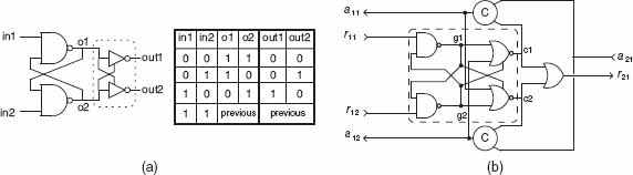
Figure 12.6 Implementation of a two-input arbiter gate. The core of the arbiter gate is the mutual-exclusive element (ME) block shown with its corresponding truth table in (a). The inverters in the ME are replaced by NOR gates in the input arbiter gate (b). Mitra (2008). Reproduced with permission of Srinjoy Mitra
The critical condition comes when both inputs in1 and in2 go high around the same time. The NAND outputs can temporarily go into a metastable state before the outputs settle into the eventual logic 0 and 1 case. The metastability comes from the inherent asymmetry of the physical implementation of the gates (Martin et al. 2003; Mitra 2008). The amount of time needed for the gate outputs to reach the final logic values depends on the time difference between both requests going high. A subsequent set of inverter gates which are powered by the outputs of the NAND gates ensure that the metastable outputs are not seen at the next stage. This metastable state can theoretically last for a long time but in practice, the circuit quickly stabilizes to the final logic values (Martin et al. 2003).
Two-Input Arbiter Gate
The operation of this gate, shown in Figure 12.6b, goes as follows: when one of the input requests becomes active (r11 = 1), c1 goes high only if the acknowledge of the other input a12 is not active, that is, a12 = 0, thus ensuring that a second handshaking cycle is not initiated by this gate when it is in the middle of the handshaking cycle of its other input r12. The output of the gate r21 goes high when either c1 or c2 is high. The corresponding input acknowledge goes high when the acknowledge from the next level of arbitration a21 goes high. The C-element gates ensure that both c1 and a21 (and c2 and a21) go through the 4-phase handshaking cycle.
The ping-pong diagram of the timing of the handshaking signals between the first two levels of arbitration in the arbiter tree of Figure 12.5 is shown in Figure 12.7. The timing example illustrates the Set and Reset phases of the input request r11 after its activation and assumes that the arbiter tree only has two levels of arbitration (i.e., N = 2). If the input request r12 to gate A1 and r13 to the gate A2 become active during either the Set or Reset phase of r11, then the requests will not be serviced till after the Reset phase of r11. After the inactivation of the acknowledge signal a21 by gate B1, this gate is free to arbitrate again between its two active input requests r21 and r22. If it chooses r22, then the Set and Reset phases of the activation of r13 are as shown at the bottom of the ping-pong diagram.
The communication cycle of this arbiter is slow because the arbiter block at the first level has to wait till the handshaking cycle is completed in all the communicating processes of the arbiter tree before the acknowledge signal to this arbiter is activated. This design was used in the very early neuromorphic chips, including the retina of Mahowald (1994).

Figure 12.7 Timing of the handshaking signals between the first two levels of arbitration in Figure 12.5. The filled and unfilled black arrows show the activation of the handshaking signals of the arbiter gate A1 (r, a11 to r, a12 and r, a21). The dashed arrows show the request and acknowledge signals for A2 (r, a13). The inactivation of the handshaking signals in the reset phase are indicated by circles. The handshaking signals between the arbiter gates A1 and A2 to the arbiter gate B1 are depicted by (r, a21 to r, a22). The labels A1, A2, and B1 refer to the gates in the arbiter tree shown in Figure 12.5. The Set and Reset phases for the activation of r11 and r13 are shown below the ping-pong diagram. Adapted from Mitra (2008) with permission of Srinjoy Mitra
Unfair Arbiter
The original arbiter circuit was modified by Boahen (2000) to allow faster transmission of address events off-chip (see Figure 12.8). The core block is a modified version of the ME element and the circuit uses mostly standard logic blocks. When r11 is active, then the output NOR gate consisting of M1 to M4 will drive r21 high if the input to Mr is high, that is, the acknowledge a21 to this gate is inactive. Notice that a1 and a2 are still inactive until a21 becomes active. When a21 is active, then with the low state of g1, a1 becomes active and together with the active r21, a11 becomes active. In this design, even if r13 becomes active before r12 as shown in Figure 12.8b before the request from r11 enters the Reset phase, r21 remains active as long as both the inputs to M1 and M2 are not low. As long as the alternate input request to gate A1 becomes active during the Set phase of the other input request, the request of another row will not be serviced thus reducing the handshaking time of the pixel by not having to switch to a different row. One disadvantage of this arbiter design is that a row with high activity tends to hold on to the arbitration bus leading to the transmission of events from only part of the chip.
Fair Arbiter
Boahen proposed a fair arbiter circuit to replace the greedy arbiter circuit (Boahen 2004a). In this new scheme, a pixel that makes consecutive requests to the arbiter is not revisited until the rest of the tree has been serviced (see Figure 12.9). The new circuits also include a pipelining scheme, which allows new requests to propagate up the tree while old ones are still being serviced at the lower levels. These arbiter cells do not need to wait for requests from their parents to be cleared before resetting their acknowledge signals as seen in Figure 12.9b where c1 (output of the aC gate connected to r11) ORed together with c2 acts as the request to the next level of arbitration. In the timing diagram, we see that after acknowledge a11 is inactivated and even after r11 becomes active again, the request r21 goes low only after r12 goes low. This request is not serviced again because c1 cannot be set high by the aC gate unless na21 is also high.

Figure 12.8 Unfair arbiter. (a) Circuit blocks for 2-input arbiter gate A1. (b) Timing diagram of a 2-level arbitration. The request r21 from A1 to the next stage stays active as long as r11 or r12 is active. The acknowledge a21 is inactivated only if neither r11 or r12 is active. The active request r13 to the A2 arbiter gate will not be serviced until both request inputs of gate A1 are inactivated. Adapted from Mitra (2008) with permission of Srinjoy Mitra
Figure 12.10 show the recorded AER spikes from two 32 × 32 multineuron chips with different arbiter types, an unfair arbiter and a fair arbiter. The spikes are in response to a common input current injected into all neurons. What is expected of the output is an identical recorded firing rate (except for mismatch) from all neurons but as we can see in the case of the unfair arbiter in (a), only spikes from half of the array were serviced by the arbiter. As the input current increases thus more spikes (and requests) are generated, the arbiter only serviced now a quarter of the array (b). In the case of the chip with a fair arbiter, we see a profile where all pixels show a more even distributed recorded rate demonstrating that the pixels are serviced roughly equally often, even with high pixel firing rates as shown in (c)-(d). The maximum spike rate of each pixel is limited by the refractory period of the event-generating circuit within the pixel.

Figure 12.9 Fair arbiter. (a) Circuit blocks for 2-input arbiter gate A1. The output of the asymmetric C-element (aC) goes high only when both r11 and na21 are high but it goes low when r11 is low. (b) Timing diagram for the same 2-level arbitration cycle. Adapted from Mitra (2008) with permission of Srinjoy Mitra
12.2.3 Other AER Blocks
The AER arbiter interface block provides an interface between either the row or column Req and Ack lines from the 2D array, the arbiter, and the chip-level handshaking signal nCXAck. Figure 12.11 shows the interface circuits between the nRR and RA lines and the signals to the arbiter. The interface circuits ensure that a new row can be selected by the arbiter only after the address of the sending pixel has been transmitted and recorded off-chip.

Figure 12.10 AER spikes recorded from two aVLSI chips using an unfair (a)–(b) and a fair arbiter (c)–(d), respectively. The figures show how the profile of recorded spikes resulting from a higher spike rate from all neurons receiving a common input current changes depending on the type of on-chip arbiter. Maximum spike rate is 1k events/second per pixel. Adapted from Mitra (2008) with permission of Srinjoy Mitra

Figure 12.11 Arbiter interface circuit between the row request and the arbiter. The circuit in (a) shows how an active low nRR signal generates a request to the arbiter (ri). The pFET driven by ReqPu returns nRR high when no pixels are requesting. The request to the arbiter is not taken away until nCXAck becomes inactive. The circuit in (b) activates RA only if the arbiter returns an active acknowledge (ai) and nCXAck is inactive. The staticizers (the feedback inverters within the dotted boxes) and transistors M1 to M3 in (a) and (b) form asymmetric C-elements

Figure 12.12 One-dimensional encoder circuit. An active high Row line pulls down the corresponding Out bit line through the connected n-channel FET (nFET). Any active Row line will drive CXReq high
In addition, the row and column lines are encoded into a digital address. AER encoders were previously discussed in Section 2.2.1 of Chapter 2. The encoding circuit in Figure 12.12 takes m input lines and transforms the inputs into n = ⌈log2(m)⌉ bits of output address. Every Row line or its complement drives the corresponding Out line through an nFET or pFET. The chip request CXREQ is driven high by any active Row for a 1D array and any active Col for a 2D array.
12.2.4 Combined Operation
The control signal flow between the various blocks in the transmitter is shown in Figure 12.13. The pixel makes a request to the arbiter through RR. Once it has received an active RA, it activates CR. Once CA is active, CXREQ is activated and the encoded pixel address is also ready for transmission. When the handshaking logic receives the corresponding active CXACK, both RA and CA are inactivated. The inactivation of CA leads to the inactivation of CXREQ and the inactivation of CXACK from the receiver. Only after the completion of the chip-level handshaking cycle can the interface handshaking block allow the next request and acknowledge cycle between the pixel and the arbiter to start again.
This timing follows the word parallel AER protocol described in Section 2.4.3 of Chapter 2. A faster readout scheme known as the word serial addressing scheme (Section 2.4.4 of Chapter 2) sends one row address and then column addresses of all active pixels on this row (Boahen 2004c).

Figure 12.13 Timing of request and acknowledge signals for all blocks in the transmitter following the word-parallel signal protocol. © 2008. IEEE. Reprinted, with permission, from Lichtsteiner et al. (2008)
12.3 AER Receiver Blocks
The schematic of the various on-chip AER blocks for a receiver with a 2D array is shown in Figure 12.14. The control path depicts how the chip-level handshaking signals CXREQ and CXACK are handled and the data path depicts how the address bits are handled in conjunction with the handshaking signals. These different blocks are discussed in more detail in Section 12.3.1 to Section 12.3.3.
12.3.1 Chip-Level Handshaking Block
The chip-level handshaking block handles the communication between the external transmitter (sender) and the chip (receiver). The chip-level handshaking signals of the receiver consist of CRREQ, CRACK, and the digital pixel address as shown in Figure 12.1. In an array of multineuron chips, this digital address encodes a unique synapse and neuron address on chip.
The communication between the handshaking block and the decoder in the circuits presented here follows the 4-phase handshaking protocol. The CRACK is normally activated as quickly as possible after CRREQ is active. This CRACK signal is also used to latch the address bits. There are two ways in which the CRACK is inactivated once CRREQ becomes inactive. The first approach used to speed up the communication time in early neuromorphic chips and still in use in many current chips is to inactivate CRACK as soon as CRREQ is inactivated. This violation of the handshaking protocol (since there is no check whether the decoded address has reached a pixel) is done on the assumption that the communication between the remaining blocks on-chip will be faster than the communication between the sender and the receiver.
This violation should not affect the communication of the address to the targeted pixel on-chip but if the communication on-chip slows down, subsequent address events from the transmitter will be affected. In that situation, the user has to determine whether the loss of spikes that come close together in time, for example, events that come in a burst even if the overall event rate is below the bus bandwidth, is a problem for the application. The second approach assures that the pixel did receive the spike by the use of additional circuits that generate a PixAck signal which is activated by the pixel which receives both active CA and RA signals. The PixAck circuits are described in Section 12.3.3. The PixAck signal from all pixels are then combined together with an inactive CRREQ to drive the inactivation of CRACK.

Figure 12.14 Schematic of the AER blocks within the receiver. When CRREQ is active and CRACK is inactive, then CRACK and Dr becomes active. The address bits are latched by Dr. The pre-decoder blocks decode the latched bits and the outputs of the pre-decoder blocks are then combined across the N outputs of the pre-decoder blocks using the 1 of N combinational logic to select one active row address. A similar operation is carried out in the X-latch and decoder. The selected pixel activates the row request line RR. The row request signals are then OR’ed together. The active pull-up M1 is driven by Pr. This pullup is inactivated when CRACK is inactive. Once one of the row request lines is activated, nPa is activated, leading to an inactivation of CRACK when CRREQ is inactive. Adapted from Mitra (2008) with permission of Srinjoy Mitra
12.3.2 Decoder
The decoder converts the latched N bit address into a one hot-code of 2N lines corresponding usually to the address of a pixel within an array. The address bits are first latched by using the CRACK signal and its complement. These bits then drive decoder circuits. The early decoder circuits used a long chain of AND transistors as shown in Figure 12.15 (Boahen 2000; Mahowald 1994). The advantage of this decoding style is the simplicity of the design. However as arrays grow in size, this decoding circuit suffers from the increased capacitance that the address lines see and the wiring capacitance that each decoding gate has to drive. These capacitance issues are described in Mead and Conway (1980) and further discussed in Mitra (2008). By adopting a decoding style used for example in large memories, the capacitance issue can be minimized in large arrays. Newer pre-decoder circuits decode the N address bits through a combination of two to four pre-decoder blocks and three to eight pre-decoder blocks. The two to four pre-decoder block consists of a set of 2-input NAND gates (an example is shown in the Y-decoder block of Figure 12.14) and the three to eight pre-decoder block uses a set of 3-input NAND gates.

Figure 12.15 Decoder circuits which take n input In bit lines and output m + 1 Row lines. The Latch signal is generated from CRACK
12.3.3 Handshaking Circuits in Receiver Pixel
The pixel includes circuits, which on activation of its CA and RA input signals generate an active nPixAck pulse. An example circuit is shown in Figure 12.16. The ANDing of CA and RA can be used as an input spike in the case of a synapse pixel. M1 biased by Vpu returns nPixAck to Vdd after CA and RA go away. M4 is part of a wired NOR along the row with a single pulldown nFET at the end of the row; RR is low in the inactive state and is pulled high when any pixel has received an input. Transistors M5 to M8 and Csyn form a current-mirror, diode-connected synapse. The transistor M5 biased by Vw determines the synapse current Iout that flows to the neuron membrane potential.
The circuit eliminates the problem whereby high-frequency switching of either RA or CA alone can lead to M2 turning on through the small parasitic capacitance, Cp2 (Boahen 1998). If M5 were connected in series with M2 and M3, Iout can flow even though only one of the transistors M2 or M3 is turned on. This current can be much larger than the pA current levels typical of synaptic currents.
This circuit also eliminates the problem of capacitive turn-on, which happens when the CA line switches a lot and the voltage changes are transmitted to the nPixAck node through the drain-gate overlap capacitance, Cp1, bringing its voltage to a few tenths of a volt below ground. Current can flow through transistor M5 even if Vw is at ground. In this design, the source voltage of M5 is brought to Vdd when the pixel is not selected.

Figure 12.16 Handshaking circuits in a pixel with a synapse. The transistor M1 driven by Vpu together with transistors M2 and M3 produce a digital output swing on nPixAck and ensure nPixAck will not be charged through capacitive coupling. Transistors M5 to M8 form a current-mirror integrator synapse. The output current of the synapse Iout, flows only when the pixel is selected
12.3.4 Pulse Extender Circuits
Because of the requirement for the AER handshaking circuits to have a short latency (<10 ns), the use of the pulse from the Figure 12.16 as the input pulse is too short for a synapse circuit to generate a finite rise and fall time in the order of milliseconds and also allowing for subthreshold currents.
12.3.5 Receiver Array Peripheral Handshaking Circuits
Receiver array peripheral handshaking circuits ensure that a pixel receives its decoded address before CRACK is inactivated at the chip level. The row request RR lines each have an active pulldown circuit that is driven by nPr, a signal which is generated by the chip-level C-element in Figure 12.14 and is a delayed version of the CRACK signal. The row RR signals drive another wired-OR global line which has an active pullup driven by Pr. When CRACK is activated, the active pulldowns of the row lines and the active pullups of the global array acknowledge line are disabled. Pr goes high, thus preventing it from pulling up the array acknowledge signal nPa. Any decoded pixel will pull its corresponding RR line high and the global line nPa low. This transition then leads to the inactivation of the CRACK once the CRREQ signal is also inactivated.
12.4 Discussion
The design of asynchronous circuits is not easy because of the lack of accessible and comprehensive design tools. The asynchronous tools assume logic signals without any assumption of rise and fall times in the physical circuits. On the physical device, signals can transition over a time of several tens to hundred nanoseconds depending on the wiring and parasitic capacitances. In such cases, the asynchronous design can fail at the silicon level if the transitioning order of signals is not preserved. Additional inverters are needed to sharpen up the edges of the signals which see large capacitances but the slow changing inputs to the inverters will also lead to higher power consumption.
As designs scale to larger arrays, the row and column line capacitances can lead to significant rise times and fall times for the logic signals and in addition a difference between the rise time of a global signal seen on one side of the array versus the other side of the array. To circumvent such problems, circuits have to be designed for example, in such a way as to ensure that pixels on both edges of the array have seen the level changes in the row and column request and acknowledge lines before the next sequence of handshaking signaling is carried out as shown in Figure 12.17.
Another area of improvement is to move from the bundled-data protocol which is delay-sensitive to an AER link which is delay-insensitive. The first step is to go to a dual-rail encoding scheme for the signals as in normal asynchronous circuits. In this scheme, each signal uses two lines, a valid signal of 1 leads to one line going high and a valid signal of 0 leads to the other line going high. An invalid signal leads to both lines being low and an incomplete signal is indicated by both lines being high. In the communication of the address bits between a transmitter and receiver, the ChipReq signal can be removed and the global address bits can be combined together to create an equivalent of a ChipReq (Martin and Nyström 2006). In this way, there is no delay which needs to be specifically introduced in the generation of the ChipReq.
A second scheme is to use a one-hot code for encoding the addresses off-chip. A one-hot code uses 2b lines in encoding b bits. For example, the four combinations of two bits are encoded by four lines. Every combination is then indicated by the activation of only one of the four lines. The address bus is then divided into groups of four where one out of four bits is activated in each group. The validity and neutrality of the different groups can be checked by a binary tree of m 4-input OR gates (if only groups of one in four are used). This scheme was first introduced in the design of Neurogrid (Lin and Boahen 2009). The authors suggested that they could also save in the number of power pads which are normally interleaved between each address bit pad by using the one-hot code scheme as the address space scales up.
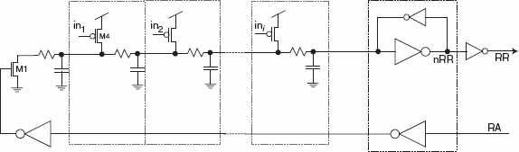
Figure 12.17 Wired OR for the row requests with an active pulldown. In the receiver, the in signals driving the pFETs come from the local nPixAcks. Because of the resistance and capacitance of the row lines, the use of an active pulldown M1 at the far end of the line is needed to guarantee correct behavior
Finally, the AER bandwidth of the chip can affect system specifications and continual improvement is needed in both the signalling and the circuit domains. Even though the cycle time for a read-out has decreased from 2 μs (computed for a 64 × 64 array in a 2 μm process) (Mahowald 1992) to a range of 30–400 ns (computed for a 104 × 96 array in a 1.2 μm process) (Boahen 1999), this bandwidth needs to be increased as arrays scale up to more than a million pixels. The AER circuits to implement a word-serial readout as described in Boahen (2004a, 2004b, 2004c) (and briefly summarized in Section 2.4.4 of Chapter 2) are examples of improvements in AER readout to increase bandwidth.
References
Boahen KA. 1998. Communicating neuronal ensembles between neuromorphic chips. In: Neuromorphic Systems Engineering (ed. Lande TS). The International Series in Engineering and Computer Science, vol. 447. Springer. pp. 229–259.
Boahen KA. 1999. A throughput-on-demand address-event transmitter for neuromorphic chips. Proc. 20th Anniversary Conf. Adv. Res. VLSI, Atlanta, GA, pp. 72–86.
Boahen KA. 2000. Point-to-point connectivity between neuromorphic chips using address-events. IEEE Trans. Circuits Syst. II 47(5), 416–434.
Boahen KA. 2004a. A burst-mode word-serial address-event link—I: transmitter design. IEEE Trans. Circuits Syst. I: Reg. Papers 51(7), 1269–1280.
Boahen KA. 2004b. A burst-mode word-serial address-event link—II: receiver design. IEEE Trans. Circuits Syst. I: Reg. Papers 51(7), 1281–1291.
Boahen KA. 2004c. A burst-mode word-serial address-event link—III: analysis and test results. IEEE Trans. Circuits Syst. I: Reg. Papers 51(7), 1292–1300.
Lichtsteiner P, Posch C and Delbrück T. 2008. A 128×128 120dB 15us latency asynchronous temporal contrast vision sensor. IEEE J. Solid-State Circuits 43(2), 566–576.
Lin J and Boahen K. 2009. A delay-insensitive address-event link. Proc. 15th IEEE Symp. Asynchronous Circuits Syst. (ASYNC), pp. 55–62.
Mahowald M. 1992. VLSI Analogs of Neural Visual Processing: A Synthesis of Form and Function. PhD thesis. California Institute of Technology, Pasadena, CA.
Mahowald M. 1994. An Analog VLSI System for Stereoscopic Vision. Kluwer Academic, Boston.
Martin AJ. 1986. Compiling communicating processes into delay-insensitive VLSI circuits. Distrib. Comput. 1, 226–234.
Martin AJ and Nyström M. 2006. Asynchronous techniques for system-on-chip design. Proc. IEEE 94(6), 1089–1120.
Martin AJ, Burns SM, Lee TK, Borkovic D, and Hazewindus PJ. 1989. The design of an asynchronous microprocessor. Advanced Research in VLSI: Proceedings of the Decennial Caltech Conference, pp. 351–373.
Martin AJ, Nyström M, and Wong C. 2003. Three generations of asynchronous microprocessors. IEEE Des. Test Comput. 20(6), 9–17.
Mead CA and Conway L. 1980. Introduction to VLSI Systems. Addison-Wesley, Reading, MA.
Mitra S 2008 Learning to Classify Complex Patterns Using a VLSI Network of Spiking Neurons. PhD thesis. ETH Zurich.
Muller DE and Bartky WS. 1959. A theory of asynchronous circuits. Proc. Int. Symp. Theory of Switching, Part 1, pp. 204–243.
Sivilotti M. 1991. Wiring Considerations in Analog VLSI Systems with Application to Field-Programmable Networks. PhD thesis. California Institute of Technology, Pasadena, CA.
Sutherland IE. 1989. Micropipelines. Communications of the ACM 32(6), 720–738.
__________
1 Some of the text and figures in this section are adapted from Mitra (2008). Reproduced with permission of Srinjoy Mitra.