
8
Silicon Synapses

Synapses form the connections between biological neurons and so can form connections between the silicon neurons described in Chapter 7. They are fundamental elements for computation and information transfer in both real and artificial neural systems. While modeling, the nonlinear properties and the dynamics of real synapses can be extremely onerous for software simulations, neuromorphic very large scale integration (VLSI) circuits efficiently reproduce synaptic dynamics in real-time. VLSI synapse circuits convert input spikes into analog charge which then produces post-synaptic currents that get integrated at the membrane capacitance of the post-synaptic neuron. This chapter discusses various circuit strategies used in implementing the temporal dynamics observed in real synapses. It also presents circuits that implement nonlinear effects with short-term dynamics, such as short-term depression and facilitation, as well as long-term dynamics such as spike-based learning mechanisms for updating the weight of a synapse for learning systems such as the ones discussed in Chapter 6 and the nonvolatile weight storage and update using floating-gate technology discussed in Chapter 10.
__________
The picture is an electron micrograph of mouse somatosensory cortex, arrowheads point to post-synaptic densities. Reproduced with permission of Nuno da Costa, John Anderson, and Kevan Martin.
8.1 Introduction
The biological synapse is a complex molecular machine. There are two main classes of synapses: Electrical synapses and chemical synapses. The circuits in this chapter implement the latter class. A simplified picture of how the chemical synapse works is shown in Figure 8.1. In a chemical synapse, the pre-synaptic and post-synaptic membranes are separated by extracellular space called a synaptic cleft. The arrival of a pre-synaptic action potential triggers the influx of Ca2+, which then leads to the release of neurotransmitter into the synaptic cleft. These neurotransmitter molecules (e.g., AMPA, GABA) bind to receptors on the post-synaptic side. These receptors consist of membrane channels with two major classes: ionic ligand-gated membrane channels such as AMPA channels with ions like Na+ and K+ and ionic ligand-gated and voltage-gated channels such as NMDA channels. These channels can be excitatory or inhibitory, that is the post-synaptic current can charge or discharge the membrane. The typical receptors in the cortex are AMPA and NMDA receptors which are excitatory and GABA receptors which are inhibitory. The post-synaptic currents produce a change in the post-synaptic potential and when this potential exceeds a threshold at the cell body of the neuron, the neuron generates an action potential.
A framework in which to describe the neurotransmitter kinetics of the synapse was proposed by Destexhe et al. (1998). Using this approach, one can synthesize equations for a complete description of the synaptic transmission process. For a two-state ligand-gated channel model, the neurotransmitter molecules T bind to the post-synaptic receptors modeled by the first-order kinetic scheme:
where R and TR∗ are the unbound and bound forms of the post-synaptic receptor, respectively, α and β are the forward and backward rate constants for transmitter binding, respectively. The fraction of bound receptors r is described by
If T is modeled as a short pulse, then the dynamics of r can be described by a first-order differential equation.
If the binding of the transmitter to a post-synaptic receptor directly gates the opening of an associated ion channel, the total conductance through all channels of the synapse is r multiplied by the maximal conductance of the synapse ![]() . Response saturation occurs naturally as r approaches one (all channels are open). The synaptic current Isyn is then given by
. Response saturation occurs naturally as r approaches one (all channels are open). The synaptic current Isyn is then given by
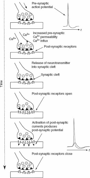
Figure 8.1 Synaptic transmission process
where Vsyn is the post-synaptic potential and Esyn is the synaptic reversal potential.
Table 8.1 Main synapse computational blocks (left), and circuit design strategies (right)
| Computational blocks | Design styles | |
| Pulse dynamics | Subthreshold | Above threshold |
| Fall-time dynamics | Voltage mode | Current mode |
| Rise- and fall-time dynamics | Asynchronous | Switched capacitor |
| Short-term plasticity | Biophysical model | Phenomenological model |
| Long-term plasticity (learning) | Real time | Accelerated time |
8.2 Silicon Synapse Implementations
In the silicon implementation, the conductance-based Eq. (8.3) is often simplified to a current that does not depend on the difference between the membrane potential and the synaptic reversal potential because the linear dependence of a current on the voltage difference across a transistor is only valid in a small voltage range of a few tenths of a volt in a subthreshold complementary metal oxide semiconductor (CMOS) circuit. Reduced synaptic models describe the post-synaptic current as a step increase in current when an input spike arrives and this current decays away exponentially when the pulse disappears.
Table 8.1 summarizes the relevant computational sub-blocks for building silicon synapses and the possible design styles that can be used to implement them. Each computational block from the first column can be implemented with circuits that adopt any of the design strategies outlined in the other column. Section 8.2.1 describes some of the more common circuits used as basic building blocks as outlined in Table 8.1.
In the synaptic circuits described in this chapter, the input is a short-duration pulse (order of μs) approximating a spike input and the synaptic output current charges the membrane capacitance of a neuron circuit.
8.2.1 Non Conductance-Based Circuits
Synaptic circuits usually implement reduced synaptic models, in part, because complex models would require many tens of transistors which would lead to a reduction in the proportional number of synapses that can be implemented on-chip. The earlier silicon synapse circuits did not usually incorporate short-term and long-term plasticity dynamics.
Pulse Current-Source Synapse
The pulsed current-source synapse is one of the simplest synaptic circuits (Mead 1989). As shown in Figure 8.2a, the circuits consist of a voltage-controlled subthreshold current source transistor in series with a switching transistor activated by an active-low input spike. The activation is controlled by the input spike (digital pulse between Vdd and Gnd) going to the gate of the Mpre transistor. When an input spike arrives, the Mpre transistor is switched on, and the output current Isyn is a current that is set by Vw (synaptic weight) of the Mw transistor. This current lasts as long as the input spike is low. Assuming that the current source transistor Mw is in saturation and the current is subthreshold, the synaptic current Isyn can be expressed as follows:

Figure 8.2 (a) Pulsed current synapse circuit and (b) reset-and-discharge circuit
where Vdd is the power supply voltage, I0 is the leakage current, κ is the subthreshold slope factor, and UT the thermal voltage (Liu et al. 2002). The post-synaptic membrane potential undergoes a step voltage change in proportion to IsynΔt, where Δt is the pulse width of the input spike.
This circuit is compact but does not incorporate any dynamics of the current. The temporal interval between input spikes does not affect the post-synaptic integration assuming that the membrane does not have a time constant; hence, input spike trains with the same mean rates but different spike timing distributions lead to the same output neuronal firing rates. However, because of its simplicity and area compactness, this circuit has been used in a wide variety of VLSI implementations of pulse-based neural networks that use mean firing rates as the neural code (Chicca et al. 2003; Fusi et al. 2000; Murray 1998).
Reset-and-Discharge Synapse
This circuit can be extended to include simple dynamics by extending the duration of the output current Isyn past the input spike duration (Lazzaro et al. 1994). This synapse circuit (Figure 8.2b) comprises three pFET transistors and one capacitor; Mpre acts as a digital switch that is controlled by the input spike; Mτ is operated as a constant subthreshold current source to recharge the capacitor Csyn; Msyn generates an output current that is exponentially dependent on the Vsyn node (assuming subthreshold operation and saturation of Msyn):
When an active-low input spike (pulse goes from Vdd to Gnd) arrives at the gate of the Mpre transistor, this transistor is switched on and the Vsyn node is shorted to the weight bias voltage Vw. When the input pulse ends (digital pulse goes from Gnd to Vdd), Mpre is switched off. Since Iτ is a constant current, Vsyn charges linearly back to Vdd at a rate set by Iτ / Csyn. The output current is
where ![]() and
and ![]() .
.
Although this synaptic circuit produces an excitatory post-synaptic current (EPSC) that lasts longer than the duration of an input pulse and decays exponentially with time, it sums nonlinearly the contribution of all input spikes. If an input spike arrives while Vsyn is still charging back to Vdd, its voltage will be reset back to Vw, thus the remaining charge contribution from the last spike will be eliminated. So, given a generic spike sequence of n spikes, ρ(t) = ![]() the response of the reset-and-discharge synapse will be
the response of the reset-and-discharge synapse will be ![]() . Although this circuit produces an EPSC that lasts longer than the duration of its input spikes, its response depends mostly on the last (nth) input spike. This nonlinear property of the circuit fails to reproduce the linear summation property of post-synaptic currents often desired in synaptic models.
. Although this circuit produces an EPSC that lasts longer than the duration of its input spikes, its response depends mostly on the last (nth) input spike. This nonlinear property of the circuit fails to reproduce the linear summation property of post-synaptic currents often desired in synaptic models.
Linear Charge-and-Discharge Synapse
Figure 8.3a shows a modification of the reset-and-discharge synapse that has often been used in the neuromorphic engineering community (Arthur and Boahen 2004). The linear charge-and-discharge synapse circuit allows for both a rise time and fall time of the output current. The circuit operation is as follows: the input pre-synaptic pulse applied to the nFET Mpre is highly active. The following analysis is based on the assumption that all transistors are in saturation and operate in subthreshold. During an input pulse, the node Vsyn(t) decreases linearly at a rate set by the net current Iw − Iτ, and the output current Isyn(t) can be described as

where ![]() is the time at which the ith input spike arrives,
is the time at which the ith input spike arrives, ![]() is the time right after the spike,
is the time right after the spike, ![]() is the output current at
is the output current at ![]() is the output current at
is the output current at ![]() , and
, and ![]() . The dynamics of the output current are exponential.
. The dynamics of the output current are exponential.

Figure 8.3 (a) Linear charge-and-discharge synapse and (b) current-mirror integrator (CMI) synapse
Assuming that each spike lasts a fixed brief period Δt, and that two successive spikes that arrive at times ti and ti+1, we can then write
From this recursive equation, we derive the response of the linear charge-and-discharge synapse to a generic spike sequence ρ(t) assuming the initial condition Vsyn(0) = Vdd. If we denote the input spike train frequency at time t as f, we can express Eq. (8.8) as
The major drawback of this circuit, aside from it not being a linear integrator, is that Vsyn is a high impedance node; so if the input frequency is too high (i.e., if f > ![]() in Eq. (8.9)), Vsyn(t) can drop to arbitrarily low values, even all the way down to Gnd. Under these conditions, the circuit’s steady-state response will not encode the input frequency. The input charge dynamics is also sensitive to the jitter in the input pulse width like all the preceding synapses.
in Eq. (8.9)), Vsyn(t) can drop to arbitrarily low values, even all the way down to Gnd. Under these conditions, the circuit’s steady-state response will not encode the input frequency. The input charge dynamics is also sensitive to the jitter in the input pulse width like all the preceding synapses.
Current-Mirror Integrator Synapse
By replacing the Mτ transistor (Figure 8.3b) with a diode-connected transistor, this modified circuit by Boahen (1997) has a dramatically different synaptic response. The two transistors Mτ and Msyn implement a current mirror, and together with the capacitor Csyn, they form a current-mirror integrator (CMI). This nonlinear integrator circuit produces a mean output current Isyn that increases with input firing rates and has a saturating nonlinearity with a maximum amplitude that depends on the circuit parameters: the weight, Vw, and the time constant bias, Vτ. The CMI responses have been derived analytically for steady-state conditions where (Hynna and Boahen 2001) and also for a generic spike train (Chicca 2006). The output current in response to an input spike is

Figure 8.4 (a) CMI voltage output and (b) synaptic current output in response to a 100-Hz input spike train
where ![]() are previously defined in Eq. (8.7),
are previously defined in Eq. (8.7), ![]() , and τd = ατc. A simulation of the voltage (Vsyn) and current (Isyn) responses from this circuit are shown in Figure 8.4.
, and τd = ατc. A simulation of the voltage (Vsyn) and current (Isyn) responses from this circuit are shown in Figure 8.4.
During the charging phase, the EPSC increases over time as a sigmoidal function, while during the discharge phase it decreases with a 1 / t profile. The discharge of the EPSC is therefore fast compared to the typical exponential decay profiles of other synaptic circuits. The parameter α (set by the Vτ source bias voltage) can be used to slow the EPSC decay. However, this parameter affects the duration of the EPSC discharge profile, the maximum amplitude of the EPSC charge phase, and the DC synaptic current; thus, longer response times (larger values of τd) produce higher EPSC values.
Despite these nonlinearities and the fact that the CMI cannot produce linear summation of post-synaptic currents, this compact circuit was extensively used by the neuromorphic engineering community (Boahen 1998; Horiuchi and Hynna 2001; Indiveri 2000; Liu et al. 2001).
Summating Exponential Synapse
The reset-and-discharge circuit was modified by Shi and Horiuchi (2004) so that the charge contribution from multiple input spikes can be summed together linearly. This summing synapse subthreshold circuit is shown in Figure 8.5. Input voltage spikes are applied to the gate Vpre of the transistor M1. Here, the gate voltage Vτ sets the time constant of the synapse as in the other synapse circuits. Vw determines the synaptic weight indirectly through a source follower acting as a level shifter. The bias current in the source follower is set by a copy of the output synaptic current Isyn. When multiple input spikes arrive at M1, the increasing Isyn reduces the value of Vx through the source follower. By applying the translinear principle discussed in Section 8.2.1,
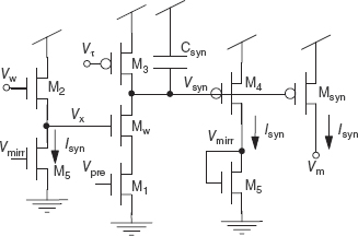
Figure 8.5 Summating synapse circuit. Input spikes are applied to Vpre. There are two control parameters. The voltage Vw adjusts the weight of the synapse indirectly through a source-follower circuit and Vτ sets the time constant. To reduce the body effect in the n-type source follower, all transistors can be converted to the opposite polarity
Log-Domain Synapse
This section covers synaptic circuits which are based on the log-domain, current-mode filter design methodology proposed by Frey (1993 1996); Seevinck (1990). These filter circuits exploit the logarithmic relationship between a subthreshold metal oxide semiconductor field effect transistor (MOSFET) gate-to-source voltage and its channel current and is therefore called a log-domain filter. Even though the original circuits from Frey were based on bipolar transistors, the method of constructing such filters can be extended to MOS transistors operating in subthreshold.
The exponential relationship between the current and the gate-to-source voltage means that we can use the translinear principle first introduced by Gilbert (1975) to solve for the current relationships in a circuit or to construct circuits with a particular input–output transfer function. This principle is also outlined in Section 9.3.1 in Chapter 9. By considering a set of transistors connected in a closed-loop form, the following equation satisfies the voltages in the clockwise (CW) direction versus the voltages in the counter-clockwise (CCW) direction:
Figure 8.6 Log-domain integrator circuit
By substituting for I in Eq. (8.12) through the subthreshold exponential I–V relationship,
We can apply the translinear principle on the currents in the low-pass filter circuit in Figure 8.6:

leading to the following first-order differential equation between the input current Iin and output current Iout:
where ![]() .
.
Log-Domain Integrator Synapse
Unlike the log-domain integrator in Figure 8.6, the log-domain integrator synapse shown in Figure 8.7 has an input current that is activated only during an input spike (Merolla and Boahen 2004). The output current Isyn has the same exponential dependence on its gate voltage Vsyn as all other synaptic circuits (see Eq. (8.5)). The derivative of this current with respect to time is given by
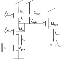
Figure 8.7 Log-domain integrator synapse circuit

During an input spike (charge phase), the dynamics of the Vsyn are governed by the equation: ![]() . Combining this first-order differential equation with Eq. (8.15), we obtain
. Combining this first-order differential equation with Eq. (8.15), we obtain
where ![]() . The beauty of this circuit lies in the fact that the term Iw is inversely proportional to Isyn itself:
. The beauty of this circuit lies in the fact that the term Iw is inversely proportional to Isyn itself:
where I0 is the leakage current and Iw0 is the current flowing through Mw in the initial condition, when Vsyn = Vdd. When this expression of Iw is substituted in Eq. (8.16), the right term of the differential equation loses the Isyn dependence and becomes the constant ![]() . Therefore, the log-domain integrator function takes the form of a canonical first-order, low-pass filter equation, and its response to a spike arriving at
. Therefore, the log-domain integrator function takes the form of a canonical first-order, low-pass filter equation, and its response to a spike arriving at ![]() and ending at
and ending at ![]() is
is
This is the only synaptic circuit of the ones described so far that has linear filtering properties. The same silicon synapse can be used to sum the contributions of spikes potentially arriving from different sources in a linear way. This could save significant amounts of silicon real estate in neural architectures where the synapses do not implement learning or local adaptation mechanisms and could therefore solve the chip area problem that have hindered the development of large-scale VLSI multineuron chips in the past.
However, the log-domain synapse circuit has two problems. The first problem is that the VLSI layout of the schematic shown in Figure 8.7 requires more area than the layout of other synaptic circuits, because the pFET Mw needs its own isolated well. The second, and more serious, problem is that the spike lengths used in pulse-based neural network systems, which typically last less than a few microseconds, are too short to inject enough charge in the membrane capacitor of the post-synaptic neuron to see any effect. The maximum amount of charge possible is ![]() and Iw0 cannot be increased beyond subthreshold current limits (of the order of nano-amperes); otherwise, the log-domain properties of the filter break down (note that Iτ is also fixed, to set the desired time constant τ). A possible solution is to increase the fast (off-chip) input pulse lengths using on-chip pulse extender circuits. This solution however requires additional circuitry at each input synapse and makes the layout of the overall circuit even larger (Merolla and Boahen 2004).
and Iw0 cannot be increased beyond subthreshold current limits (of the order of nano-amperes); otherwise, the log-domain properties of the filter break down (note that Iτ is also fixed, to set the desired time constant τ). A possible solution is to increase the fast (off-chip) input pulse lengths using on-chip pulse extender circuits. This solution however requires additional circuitry at each input synapse and makes the layout of the overall circuit even larger (Merolla and Boahen 2004).
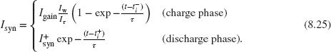
Diff-Pair Integrator Synapse
By replacing the isolated pFET Mw with three nFETs, the Diff-Pair Integrator (DPI) synapse circuit (Bartolozzi and Indiveri 2007) solves the problems of the log-domain integrator synapse while maintaining its linear filtering properties, thus preserving the possibility of multiplexing in time spikes arriving from different sources. The schematic diagram of the DPI synapse is shown in Figure 8.8. This circuit comprises four nFETs, two pFETs, and a capacitor. The nFETs form a differential pair whose branch current Iin represents the input to the synapse during the charging phase. Assuming both subthreshold operation and saturation regime, Iin can be expressed as

Figure 8.8 Diff-pair integrator synapse circuit
and by multiplying the numerator and denominator of Eq. (8.19) by e ![]() , we can re-express Iin as
, we can re-express Iin as
where the term ![]() represents a virtual p-type subthreshold current that is not tied to any pFET in the circuit.
represents a virtual p-type subthreshold current that is not tied to any pFET in the circuit.
As for the log-domain integrator, we can combine the Csyn capacitor equation ![]() −(Iin − Iτ) with Eq. (8.5) and write
−(Iin − Iτ) with Eq. (8.5) and write
where ![]() . Replacing Iin from Eq. (8.20) into Eq. (8.21), we obtain
. Replacing Iin from Eq. (8.20) into Eq. (8.21), we obtain
This is a first-order nonlinear differential equation; however, the steady-state condition can be solved in closed form and its solution is
If Iw ≫ Iτ, the output current Isyn will eventually rise to values such that Isyn ≫ Igain, when the circuit is stimulated with an input step signal. If ![]() ≫ 1, the Isyn dependence in the second term of Eq. (8.22) cancels out, and the nonlinear differential equation simplifies to the canonical first-order, low-pass filter equation:
≫ 1, the Isyn dependence in the second term of Eq. (8.22) cancels out, and the nonlinear differential equation simplifies to the canonical first-order, low-pass filter equation:
In this case, the output current response of the circuit to a spike is
The dynamics of this circuit is almost identical to the log-domain integrator synapse circuit with the difference that the term Iw / Iτ is multiplied by Igain here, rather than the I0 of the log-domain integrator solution. This gain term can be used to amplify the charge phase response amplitude, therefore solving the problem of generating sufficiently large charge packets sourced into the neuron’s integrating capacitor for input spikes of very brief duration, while keeping all currents in the subthreshold regime and without requiring additional pulse-extender circuits. An additional advantage of this circuit over the log-domain one is given by the fact that the layout of the circuit does not require isolated well structures for the pFETs.
Although this circuit is less compact than many synaptic circuits, it is the only one that can reproduce the exponential dynamics observed in the post-synaptic currents of biological synapses, without requiring additional input pulse-extender circuits. Moreover, the circuit has independent control of time constant, synaptic weight, and synaptic scaling parameters. The extra degree of freedom obtained with the Vthr parameter can be used to globally scale the efficacies of the DPI circuits that share the same Vthr bias. This feature could in turn be employed to implement global homeostatic plasticity mechanisms complementary to local spike-based plasticity ones acting on the synaptic weight node Vw.
8.2.2 Conductance-Based Circuits
In the synaptic circuits described until now, the post-synaptic current Isyn is almost independent of the membrane voltage, Vm because the output of the synapse comes from the drain node of a transistor in saturation. A more detailed synaptic model that includes the dependence of the ionic current on Vm is called the conductance-based synapse. The dynamics of Vm corresponding to currents that capture this dependence is described as follows:
where Cm is the membrane capacitance, Vm is the membrane potential, gi(t) is a time-varying synaptic conductance, Ei is a synaptic reversal potential corresponding to the particular ionic current (e.g., Na+, K+), and each of the terms on the right corresponds to a particular ionic current.
Single-Transistor Synapse
A transistor, when operated in the ohmic region, can produce a post-synaptic current that is dependent on the difference between the membrane potential and the reversal potential. This relationship is approximately linear for a transistor operating in subthreshold and for drain-to-source voltages (Vds) which are less than approximately 4kT / q. Circuits that implement the conductance-based dependencies by operating the transistor under these conditions include the single-transistor synapses described by Diorio et al. (1996 1998), and the Hodgkin– Huxley circuits by Hynna and Boahen (2007) and Farquhar and Hasler (2005). By operating the transistors in strong inversion, the Vds range over which the current grows linearly is a function of the gate-source voltage, Vgs. The use of the transistor in this region is implemented in the above-threshold multineuron arrays (Schemmel et al. 2007 2008).

Figure 8.9 Single compartment switched-capacitor conductance-based synapse circuit. When the address of an incoming event is decoded, row- and column-select circuitry activate the cells neuron select (NS) line.The nonoverlapping clocks, ![]() 1 and
1 and ![]() 2, control the switching and are activated by the input event. © 2007 IEEE. Reprinted, with permission, from Vogelstein et al. (2007)
2, control the switching and are activated by the input event. © 2007 IEEE. Reprinted, with permission, from Vogelstein et al. (2007)
Switched-Capacitor Synapse
The switched-capacitor circuit in Figure 8.9 implements a discrete-time version of the conductance-based membrane equation. The dynamics for synapse i is
The conductance, gi = g is discrete in amplitude. The amount of charge transferred depends on which of the three geometrically sized synaptic weight capacitors (C0 to C2) are active. These elements are dynamically switched on and off by binary control voltages W0 − W2 on the gates of transistors M1 to M3. The binary coefficients W0 − W2 provide eight possible conductance values. A larger dynamic range in effective conductance can be accommodated by modulating the number and probability of synaptic events according to the synaptic conductance g = npq (Koch 1999). That is, the conductance is proportional to the product of the number of synaptic release sites on the pre-synaptic neuron (n), the probability of synaptic release (p), and the post-synaptic response to a quantal amount of neurotransmitter (q). By sequentially activating switches X1 and X2, a packet of charge proportional to the difference between the externally supplied and dynamically modulated reversal potential E and Vm is added to (or subtracted from) the membrane capacitor Cm.
Figure 8.10 illustrates the response of a conductance-based neuron as it receives a sequence of events through the switched-capacitor synapse while both the synaptic reversal potential and the synaptic weight are varied (Vogelstein et al. 2007). This neuron is part of an array used in the integrate-and-fire array transceiver (IFAT) system discussed in Section 13.3.1. The membrane voltage reveals the strong impact of the order of events on the neural output due to the operation of the conductance-based model, as opposed to a standard I&F model. This circuit can also implement ‘shunting inhibition’ usually observed in Cl− channels. This effect happens when the synaptic reversal potential is close to the resting potential of the neuron. Shunting inhibition results from the nonlinear interaction of neural activity gated by such a synapse, an effect that is unique to the conductance-based model and missing in both standard and leaky I&F models.

Figure 8.10 Responses from a neuron within an array of conductance-based synapses and neurons. The lower trace illustrates the membrane potential (Vm) of the neuron as a series of events sent at times marked by vertical lines at the bottom of the figure. The synaptic reversal potential (E) and synaptic weight (W) are drawn in the top two traces. An inhibitory event following a sequence of excitatory events has a greater impact on the membrane potential than the same inhibitory event following many inhibitory events (compare events indicated by arrows A versus A*) and vice versa (compare events indicated by arrows B versus B*). © 2007 IEEE. Reprinted, with permission, from Vogelstein et al. (2007)
The synaptic circuit in Figure 8.9 does not have any temporal dynamics. Extensions to this design (Yu and Cauwenberghs 2010) give this circuit the synaptic dynamics.
8.2.3 NMDA Synapse
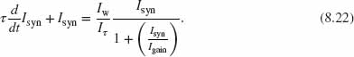
The NMDA receptors form another important class of synaptic channels. These receptors allow ions to flow through the channels only if the membrane voltage is depolarized above a given threshold while in the presence of their neurotransmitter (glutamate). A circuit that demonstrates this property by exploiting the thresholding property of the differential pair circuit is shown in Figure 8.11 (Rasche and Douglas 2001). If the membrane node Vm is lower than an external bias Vref, the output current Isyn flows through the transistor M4 in the left branch of the diff-pair and has no effect on the post-synaptic depolarization. On the other hand, if Vm is higher than Vref, the current flows also into the membrane potential node, depolarizing the neuron, and thus implementing the voltage-gating typical of NMDA synapses.
This circuit can reproduce both the voltage-gated and temporal dynamic properties of real NMDA synapses. It may be important to be able to implement these properties in our VLSI devices because there is evidence that they play a crucial role in detecting coincidence between the pre-synaptic activity and post-synaptic depolarization for inducing long-term potentiation (LTP) (Morris et al. 1990). Furthermore, the NMDA synapse could be useful for stabilizing persistent activity of recurrent VLSI networks of spiking neurons, as proposed by computational studies within the context of working memory (Wang 1999).
Figure 8.11 NMDA synapse circuit. Vm is the post-synaptic membrane voltage. The transistors, M3 and M4, of the differential pair circuit emulate the voltage dependence of the current. Input spike that goes to Vpre and Vw sets the weight of the synapse
8.3 Dynamic Plastic Synapses
The synapse circuits discussed so far have a weight that is specified by a fixed value during operation. In many biological synapses, experiments show that the effective conductance of the membrane channels in the synapse change dynamically. This change in the conductance is dependent on the pre-synaptic activity and/or the post-synaptic activity. Short-term dynamic synapse states are determined by their pre-synaptic activity and have short time constants from around tens to hundreds of milliseconds. Long time-constant plastic synapses have weights that are modified by both the pre- and post-synaptic activity. Their time constants can be in the hundreds of seconds to hours, days, and years. Their functional roles are usually explored in models of learning. The next sections describe synapse circuits where the weight of the synapse changes following either short-term or long-term plasticity.
8.3.1 Short-Term Plasticity
Dynamic synapses can be depressing, facilitating, or a combination of both. In a depressing synapse, the synaptic strength decreases after each spike and recovers to its maximal value with a time constant τd. This way, a depressing synapse is analogous to a high-pass filter. It codes primarily changes in the input rather than the absolute level of the input. The output current of the depressing synapse codes primarily changes in the pre-synaptic frequency. The steady-state current amplitude is approximately inversely dependent on the input frequency. In facilitating synapses, the strength increases after each spike and recovers to its minimum value with a time constant τf. It acts like a nonlinear low-pass filter to changes in spike rates. A step increase in pre-synaptic firing rate leads to a gradual increase in the synaptic strength.
Both types of synapses can be treated as time-invariant fading memory filters (Maass and Sontag 2000). Two prevalent models that are used in network simulations and also for fitting physiological data are the phenomenological models by Markram et al. (1997); Tsodyks and Markram (1997); Tsodyks et al. (1998) and the models from Abbott et al. (1997) and Varela et al. (1997).
In the model from Abbott et al. (1997), the depression in the synaptic weight is defined by a variable D, varying between 0 and 1. The synaptic strength is then gD(t), where g is the maximum synaptic strength. The dynamics of D is described by
where τd is the recovery time constant of the depression and D is decreased by d (d < 1), right after a spike, δ(t).
An example of a depressing circuit is shown in Figure 8.12. The circuit details and its response are described in Rasche and Hahnloser (2001) and Boegerhausen et al. (2003). The voltage Va determines the maximum synaptic strength g while the synaptic strength gD = Isyn is exponential in the voltage Vx. The subcircuit consisting of transistors M1 to M3 controls the dynamics of Vx. The spike input goes to the gate terminal of M1 and M4. During an input spike, a quantity of charge (determined by Vd) is removed from the node Vx. In between spikes, Vx recovers toward Va through the diode-connected transistor M3 (see Figure 8.13). We can convert the Isyn current source into an equivalent current Id with some gain and a time constant through the current-mirror circuit consisting of M5, Msyn, and the capacitor Csyn, and by adjusting the voltage Vgain. The synaptic strength is given by ![]() .
.
Figure 8.12 Depressing synapse circuit
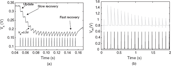
Figure 8.13 Responses measured from the depressing synapse circuit of Figure 8.12. (a) Change of Vx over time. It is decreased when an input spike arrives and it recovers back to the quiescent value at different rates dependent on its distance from the resting value, Va ≈ 0.33 V. Adapted from Boegershausen et al. (2003). Reproduced with permission of MIT Press. (b) Transient response of a neuron (by measuring its membrane potential, Vm) when stimulated by a regular spiking input (bottom curve) through a depressing synapse. The bottom trace in each subplot shows the input spike train
8.3.2 Long-Term Plasticity
In a synaptic model of short-term plasticity, the weight of the synapse is dependent on the short time history of the input spike activity. In the case of long-term plasticity, the weight is determined by both the pre-synaptic and post-synaptic activity. The VLSI circuits that implement such learning rules range from Hebbian rules to spike-timing dependent plasticity (STDP) rule and its variants. The various types of long-term plastic VLSI synapse circuits have been implemented following a general block diagram shown in Figure 8.14.
Analog Inputs for Weight Update
One of the earliest attempts in building learning synapses come out of the floating-gate circuits work in Mead’s lab in the 1990s. (There was an earlier work (Holler et al. 1989) on trainable networks). These circuits capitalize on the availability of nonvolatile memory storage mechanisms, hot-electron injection, and electron tunneling in a normal CMOS process leading to the ability to modify the memory or voltage on a floating gate (Diorio et al. 1996, 1998; Hasler 2005; Hasler et al. 1995, 2001; Liu et al. 2002). These mechanisms are further explained in Chapter 10 and an example synaptic array is shown in Figure 8.15. These nonvolatile update mechanisms are similar to the ones used in electrically erasable programmable read only memory (EEPROM) technology except that EEPROM transistors are optimized for digital programming and binary-valued data storage. The floating-gate silicon synapse has the following desirable properties: the analog memory is nonvolatile and the memory update can be bidirectional. The synapse output is the product of the input signal and the stored value. The single transistor synapse circuit essentially implements all three components of the learning synapse in Figure 8.14. Although the initial work was centered around high-threshold nFET transistors in specialized bipolar technology, similar results were obtained from pFET transistors in normal CMOS technology (Hasler et al. 1999), hence current work is centered around arrays of pFET synapses connected to various neuron models (Brink et al. 2013). Various floating-gate learning synapses that use the explicit dynamics offered by the floating-gate dynamics include the correlation-learning rules (Dugger and Hasler 2004) and later floating-gate synapses that use spike-based inputs following a STDP rule (H¨afliger and Rasche 1999; Liu and Moeckel 2008; Ramakrishnan et al. 2011). The advantage of the floating-gate technology for implementing synapses is that the parameters for the circuits can be stored using the same nonvolatile technology (Basu et al. 2010).
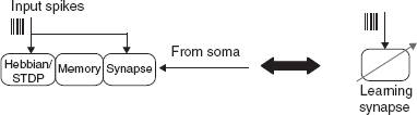
Figure 8.14 General block diagram for a learning synapse. The components are a Hebbian/STDP block which implements the learning rule, a memory block, and a synaptic circuit

Figure 8.15 A 2 × 2 synaptic array of high-threshold floating-gate transistors with circuits to update weight using tunneling and injection mechanisms. The row synapses share a common drain wire, so tunneling at synapse (1,1) is activated by raising the row 1 drain voltage to a high value and by setting col1 gate to a low value. To inject at the same synapse, col1 gate is increased and the row 1 drain voltage is lowered
Spike-Based Learning Circuits using Floating-Gate Technology
The earliest spike-based learning VLSI circuit was described by H¨afliger et al. (1996). This circuit implemented a spike-based version of the learning rule based on the Riccati equation as described by Kohonen (1984). This time-dependent learning rule (more thoroughly described in H¨afliger 2007) that the circuit is based on, achieves exact weight normalization, if the output mechanism is an I&F neuron (weight vector normalization here means that the weight vector length will always converge to a given constant length) and can detect temporal correlations in spike trains. (Input spike trains that show a peak around zero in their cross-correlograms with other inputs, i.e., they tend to fire simultaneously, will be much more likely to increase synaptic weights.)
To describe the weight update rule as a differential equation, the input spike train x to the synapse in question (and correspondingly the output spike train from the neuron y) is described as sum of Dirac delta function:
where tj is the time of the jth input spike.
Sometimes it is more convenient to use the characteristic function x′ for the set of input spikes, that is, a function that is equal to 1 at firing times and 0 otherwise.
The weight update rewards a potential causal relationship between an input spike and a subsequent action potential, that is, when an action potential follows an input spike. This is very much in the spirit of Hebb’s original postulate which says that an input ‘causing’ an action potential should lead to an increase in synaptic weight (Hebb 1949). On the other hand, if an action potential is not preceded by a synaptic input, that weight shall tend to be decreased. To implement this, a ‘correlation signal’ c is introduced for each synapse. Its purpose is to keep track of recent input activity. Its dynamics is described as follows:
The correlation signal c at a synapse is incremented by 1 for every input spike, decays exponentially with time constant τ, and is reset to 0 with every output spike.
This equation has been approximated in H¨afliger (2007) with the circuit in Figure 8.16. An active-low input spike ‘nPre’ activates the current source transistor (M2) biased by ‘nInc’ and increments the voltage on node ‘corr’ which represents the variable c. This voltage is subject to the leakage current through M5. This constant leakage current constitutes the main difference to the theoretical rule, because it is not a resistive current. An output spike causes the signal ‘Ap’ to go high for a few microseconds. During this time, ‘corr’ is reset through M3 and M4. These signal dynamics are illustrated in the inset in the upper right of Figure 8.16.
The theoretical weight update rule originally proposed in H¨afliger et al. (1996) but more conveniently described in H¨afliger (2007) rewards causal input–output relationships and punishes noncausal relationships following
At every output spike, the weight w is incremented by μc and decremented by ![]() , where μ is the learning rate and μ is the length to which the weight vector is normalized.
, where μ is the learning rate and μ is the length to which the weight vector is normalized.
Transistors M6 through M9 in Figure 8.16 compute the positive term μc of that update rule, as sampled at the onset of a neuron output pulse ‘Ap’ (which represents a spike in the spike train y): they linearly transduce the voltage on node ‘corr’ into the time domain as an active-low pulse length as illustrated in the inset on the bottom right of the figure: the signal ‘Ap’ activates the current comparator M6/M8 and its output voltage ‘nLearn up’ goes low for the time it takes ‘corr’ to reach its idle voltage ‘Corr baseline’, when depleted through the current limit set by ‘Pul len,’ that is, for a duration that is proportional to c. M6 is biased by ‘Vthreshold’ to source a current only slightly bigger than the current supplied by M8 when ‘corr’ is equal to ‘Corr baseline.’
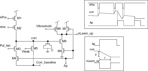
Figure 8.16 Circuit that approximates Eq. (8.30) (transistors M1, M2, and M5) and the positive weight update term of Eq. (8.31) (transistors M3 and M4, and M6 through M9). The latter is a digital pulse ‘nLearn up’ the duration of which corresponds to term c as the neuron fires. This circuit implements the module for increasing the weight (the LTP part) in the Hebbian block of Figure 8.14
So the result of this circuit is a width-modulated digital pulse in the time domain. This pulse can be connected to any kind of analog weight storage cell that increments its content proportionally to the duration of that pulse, for example, a capacitor or floating gate which integrates a current from a current source or tunneling node turned on for the duration of that pulse.
The negative update term in Eq. (8.31) is implemented in a similar manner with a width-modulated output pulse, for example, activating a negative current source on a capacitive or floating gate weight storage cell. The original circuit (H¨afliger et al. 1996) used capacitive weight storage, and later implementations were made with analog floating gate (H¨afliger and Rasche 1999), and ‘weak’ multilevel storage cells (H¨afliger 2007; Riis and H¨afliger 2004).
Spike Timing-Dependent Plasticity Rule
The spike-based learning rule previously outlined in Section 6.3.1 of Chapter 6 is also called the STDP rule. It models the behavior of synaptic plasticity observed in physiological experiments (Markram et al. 1997; Song et al. 2000; van Rossum et al. 2000). The form of this learning rule is shown in Figure 8.17. The synaptic weight is increased when the pre-synaptic spike precedes a post-synaptic spike within a time window. For the reverse order of occurrence of pre- and post-synaptic spikes, the synaptic weight is decreased. In the additive form, the change in weight A(Δt) is independent of the synaptic weight A and the weights saturate at a fixed maximum and minimum value (Abbott and Nelson 2000):
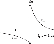
Figure 8.17 Temporally asymmetric learning curve or spike-timing-dependent plasticity curve
where tpost = tpre + Δt. In the multiplicative form, the change in weight is dependent on the synaptic weight value.
STDP Silicon Circuits
Silicon STDP circuits that emulate the weight update curves in Figure 8.17 were described in Bofill-i-Petit et al. (2002), Indiveri (2003), and Indiveri et al. (2006). The circuits in Figure 8.18 can implement both the weight-dependent and weight-independent updates (Bofill-i-Petit and Murray 2004). The weight of each synapse is represented by the charge stored on its weight capacitor Cw. The strength of the weight is inversely proportional to Vw. The closer the value of Vw is to ground, the stronger is the synapse.
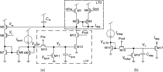
Figure 8.18 Weight change circuits. (a) Strength of the synapse is inversely proportional to the value of Vw. The higher Vw, the smaller the weight of the synapse. This section of the weight change circuit detects causal spike correlations. (b) This part of the circuit creates the decaying shape of the depression side of the learning window
The spike output of the neuron driven by the plastic synapse is defined as Post. When Pre (input spike) is active, the voltage created by Ibpot on the diode connected transistor M9 is copied to the gate of M13. This voltage across Cpot decays with time from its peak value due to a leakage current set by Vbpot. When the post-synaptic neuron fires, Post switches M12 on. Therefore, the weight is potentiated (Vw decreased) by an amount which reflects the time elapsed since the last pre-synaptic event.
The weight-dependent mechanism is introduced by the simple linearized V–I configuration consisting of M5 and M6 and the current mirror M7 and M8 (see Figure 8.18a). M5 is a low gain transistor operated in strong inversion whereas M6 is a wide transistor made to operate in weak inversion such that it has even higher gain. When Vw decreases (weight increase) the current through M5 and M6 increases, but M5 is maintained in the linear region by the high gain transistor. Thus, a current proportional to the value of the weight is subtracted from Ibpot. The resulting smaller current injected into M9 will cause a drop in the peak of potentiation for large weight values.
In a similar manner to potentiation, the weight is weakened by the circuit shown in Figure 8.18b when it detects a noncausal interaction between a pre-synaptic and a post-synaptic spike. When a post-synaptic spike event is generated, a Post pulse charges Cdep. The accumulated charge leaks linearly through M16 at a rate set by Vbdep. A nonlinear decaying current (Idep) is sent to the weight change circuits placed in the input synapse (see Idep in Figure 8.18a). When a pre-synaptic spike reaches a synapse, M1 is turned on. If this occurs soon enough after the Post pulse, Vw is brought closer to Vdd (weight strength decreased).
This circuit can be used to implement weight-independent learning by setting Vr to Vdd. Modified versions of this circuit have been used to express variants of the STDP rule, for example, the additive and multiplicative forms of the weight update as discussed in Song et al. (2000) (Bamford et al. 2012).
Binary Weighted Plastic Synapses
Stochastic Binary
The bistable synapses described in Section 6.3.2 of Chapter 6 have been implemented in analog VLSI (Fusi et al. 2000). This synapse uses an internal state represented by an analog variable that makes jumps up or down whenever a spike appears on the pre-synaptic neuron. The direction of the jump is determined by the level of depolarization of the post-synaptic neuron. The dynamics of the analog synaptic variable is similar to the perceptron rule, except that the synapse maintains its memory on long timescales in the absence of stimulation. Between spikes, the synaptic variable drifts linearly up, toward a ceiling or down, toward a floor depending on whether the variable is above or below a synaptic threshold. The two values that delimit the synaptic variable are the stable synaptic efficacies.
Because stimulation takes place on a finite (short) interval, stochasticity is generated by the variability in both the pre- and post-synaptic neurons spike timings. Long-term potentiation (LTP) and long-term depression (LTD) transitions take place on pre-synaptic bursts, when the jumps accumulate to overcome the refresh drifts. The synapse can preserve a continuous set of values for periods of the order of its intrinsic time constants. But on long timescales, only two values are preserved: the synaptic efficacy fluctuates in a band near one of the two stable values until a strong stimulation produces a enough spikes to drive it out of the band and into the neighborhood of the other stable value. The circuit shown in Figure 8.19 shows the different building blocks of the learning synapse.
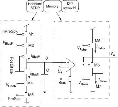
Figure 8.19 Schematic of the bistable synaptic circuit. The activity-dependent Hebbian block implements H(t). The voltage across the capacitor C is U(t) and is related to the internal variable X(t) by Eq. (8.33). The memory block implements R(t) and provides the refresh currents
The capacitor C acts as an analog memory element: the dimensionless internal synaptic state X(t) is related to the capacitor voltage in the following way:
where U(t) is the voltage across the synaptic capacitor and can vary in the region delimited by Umin ≈ 0 and Umax ≈ Vdd.
Hebbian Block
The Hebbian block implements H(t) which is activated only on the arrival of a pre-synaptic spike. The synaptic internal state jumps up or down, depending on the post-synaptic depolarization. The binary input signal PostState determines the direction of the jump and is the outcome of the comparison between two voltage levels: the depolarization of the post-synaptic neuron V(t) and the firing threshold θV. If the depolarization is above the threshold, then PostState is ≈ 0; otherwise it is near the power supply voltage Vdd. (The circuit for generating PostState is not shown). In the absence of pre-synaptic spikes, M1 and M5 are not conducting and no current flows into the capacitor, C. During the emission of a pre-synaptic spike (nPreSpk is low), the PostState signal controls which branch is activated. If PostState = 0 (the post-synaptic depolarization is above the threshold θV), current charges up the capacitor C. The charging rate is determined by VBiasP, which is the current flowing through M2. Analogously, when PostState = 1, the lower branch is activated, and the capacitor is discharged to ground.
Memory Block
The refresh block implements R(t), which charges the capacitor if the voltage U(t) is above the threshold Uθ (corresponding to θX) and discharges it otherwise. It is the term that tends to damp any small fluctuation that drives U(t) away from one of the two stable states. If U(t) < Uθ, the voltage output of the comparator is ≈ Vdd, M5 is not conducting while M6 is conducting. The result is a discharge of the capacitor by the current IRefrn. If U(t) > Uθ, the low output of the comparator turns on M5 and the capacitor is charged at a rate proportional to the difference between the currents IRefrp and IRefrn.
Stochastic Binary Stop-Learning
The spike-based learning algorithm implemented in Figure 8.19 is based on the model described in Brader et al. (2007) and Fusi et al. (2000). This algorithm can be used to implement both unsupervised and supervised learning protocols, and train neurons to act as perceptrons or binary classifiers. Typically, input patterns are encoded as sets of spike trains with different mean frequencies, while the neuron’s output firing rate represents the binary classifier output. The learning circuits that implement this algorithm can be subdivided into two main blocks: a spike-triggered weight-update module with bistable weights, present in each plastic synapse, and a post-synaptic stop-learning control module, present in the neuron’s soma. The ‘stop-learning’ circuits implement the characteristic feature of this algorithm, which stops updating weights if the output neuron has a very high or very low output firing rate, indicating the fact that the dot product between the input vector and the learned synaptic weights is either close to 1 (pattern recognized as belonging to the trained class) or close to 0 (pattern not in trained class).
The post-synaptic stop-learning control circuits are shown in Figure 8.20. These circuits produce two global signals VUP and VDN, shared among all synapses belonging to the same dendritic tree, to enable positive and/or negative weight updates respectively. Post-synaptic spikes produced by the I&F neuron are integrated by a DPI circuit. The DPI circuit produces the signal VCa which is related to the Calcium concentration in real neurons, and represents the recent spiking activity of the neuron. This signal is compared to three different thresholds (Vthk1, Vthk2, and Vthk3) by three corresponding current-mode winner-take-all circuits (Lazzaro et al. 1989). In parallel, the neuron’s membrane potential Vm is compared to a fixed threshold Vthm by a transconductance amplifier. The values of VUP and VDN depend on the output of this amplifier, as well as the Calcium concentration signal VCa. Specifically, if Vthk1 < VCa < Vthk3 and Vm > Vmth, then increases in synaptic weights (VUP < Vdd) are enabled. If Vthk1 < VCa < Vthk2 and Vmem < Vthm, then decreases in synaptic weights (VDN > 0) are enabled. Otherwise no changes in the synaptic weights are allowed (VUP = Vdd, and VDN = 0).
Figure 8.20 Post-synaptic stop-learning control circuits at the soma of neurons with bistable synapses. The winner-take-all (WTA) circuit in (a) and the DPI circuit are used in the stop-learning control circuit in (b)
Figure 8.21 Spike-based learning circuits. Pre-synaptic weight-update module or Hebbian block of each learning synapse. The signals VUP and VDN are generated by the circuit in Figure 8.20
The pre-synaptic weight-update module comprises four main blocks: an input stage (see MI1 − MI2 in Figure 8.21), a spike-triggered weight update circuit (ML1 − ML4 in Figure 8.21), a bistability weight refresh circuit (see transconductance amplifier in Figure 8.21), and a current-mode DPI circuit (not shown). The bistability weight refresh circuit is a positive-feedback amplifier with very small ‘slew-rate’ that compares the weight voltage Vw to a set threshold Vthw, and slowly drives it toward one of the two rails Vwhi or Vwlo, depending whether Vw > Vthw or Vw < Vthw, respectively. This bistable drive is continuous and its effect is superimposed to the one from the spike-triggered weight update circuit. Upon the arrival of an input address-event, two digital pulses trigger the weight update block and increase or decrease the weight, depending on the values of VUP and VDN: if during a pre-synaptic spike the VUP signal from the post-synaptic, stop-learning control module is enabled (VUP < Vdd), the synapse’s weight Vw undergoes an instantaneous increase. Similarly, if during a pre-synaptic spike the VDN signal from the post-synaptic, weight control module is high, Vw undergoes an instantaneous decrease. The amplitude of the EPSC produced by the DPI block upon the arrival of the pre-synaptic spike is proportional to VΔw.
Mitra et al. (2009) show how such circuits can be used to carry out classification tasks, and characterize the performance of this VLSI learning system. This system also displays the transition dynamics in Figure 6.3 of Chapter 6.
Binary SRAM STDP
A different method of updating the synaptic weight based on the STDP learning rule is the binary STDP synaptic circuit (Arthur and Boahen 2006). It is built from three subcircuits: the decay circuit, the integrator circuit, and static random access memory (SRAM) (Figure 8.22). The decay and integrator subcircuits are used to implement potentiation and depression in a symmetric fashion. The SRAM holds the current binary state of the synapse, either potentiated or depressed.
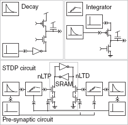
Figure 8.22 Binary static random access memory (SRAM) STDP circuit. The circuit is composed of three subcircuits: decay, integrator, and STDP SRAM. Adapted from Arthur and Boahen (2006). Reproduced with permission of MIT Press
For potentiation, the decay block remembers the last pre-synaptic spike. Its capacitor is charged when that spike occurs and discharges linearly thereafter. A post-synaptic spike samples the charge remaining on the capacitor, passes it through an exponential function, and dumps the resultant charge into the integrator. This charge decays linearly thereafter. At the time of the post-synaptic spike, the SRAM, a cross-coupled inverter pair, reads the voltage on the integrator’s capacitor. If it exceeds a threshold, the SRAM switches state from depressed to potentiated (nLTD goes high and nLTP goes low). The depression side of the STDP circuit is exactly symmetric, except that it responds to post-synaptic activation followed by pre-synaptic activation and switches the SRAM’s state from potentiated to depressed (nLTP goes high and nLTD goes low). When the SRAM is in the potentiated state, the pre-synaptic spike activates the principal neuron’s synapse; otherwise the spike has no effect. The output of the SRAM activates a log-domain synapse circuit described in Section 8.2.1.
8.4 Discussion
The historical picture of how the various synapse circuits have evolved over the years is depicted in Figure 8.23. Synaptic circuits can be more costly (in number of transistors) than a silicon neuron circuit. As more features are added, the transistor count per synapse grows. In addition, these circuits still face the difficulty of an elegant implementation of a linear resistor especially when the circuits are operated in subthreshold. Therefore, the designer should consider the necessary features needed for the application rather than building a synapse with all possible features. This chapter focuses on mixed-signal synapse circuits. An all-digital solution for both synapses and neurons has also been considered because these circuits, while dissipating more power on average, can be designed faster using existing design tools as demonstrated by Arthur et al. (2012), Merolla et al. (2011), and Seo et al. (2011).
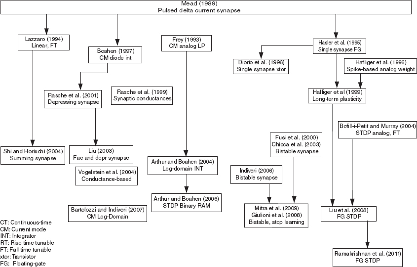
Figure8.23 Historical tree
References
Abbott LF and Nelson SB. 2000. Synaptic plasticity: taming the beast. Nat. Neurosci. 3, 1178–1183.
Abbott LF, Varela JA, Sen K, and Nelson SB. 1997. Synaptic depression and cortical gain control. Science 275(5297), 220–223.
Arthur JV and Boahen K. 2004. Recurrently connected silicon neurons with active dendrites for one-shot learning. Proc. IEEE Int. Joint Conf. Neural Netw. (IJCNN), 3, pp. 1699–1704.
Arthur JV and Boahen K. 2006. Learning in silicon: timing is everything. In: Advances in Neural Information Processing Systems 18 (NIPS) (eds Weiss Y, Schölkopf B, and Platt J). MIT Press, Cambridge, MA. pp. 75–82.
Arthur JV, Merolla PA, Akopyan F, Alvarez R, Cassidy A, Chandra S, Esser S, Imam N, Risk W, Rubin D, Manohar R, and Modha D. 2012. Building block of a programmable neuromorphic substrate: a digital neurosynaptic core. Proc. IEEE Int. Joint Conf. Neural Netw. (IJCNN), pp. 1–8.
Bamford SA, Murray AF, and Willshaw DJ. 2012. Spike-timing-dependent plasticity with weight dependence evoked from physical constraints. IEEE Trans. Biomed. Circuits Syst. 6(4), 385–398.
Bartolozzi C and Indiveri G. 2007. Synaptic dynamics in analog VLSI. Neural Comput. 19(10), 2581–2603.
Basu A, Ramakrishnan S, Petre C, Koziol S, Brink S, and Hasler PE. 2010. Neural dynamics in reconfigurable silicon. IEEE Trans. Biomed. Circuits Syst. 4(5), 311–319.
Boahen KA. 1997. Retinomorphic Vision Systems: Reverse Engineering the Vertebrate Retina. PhD thesis. California Institute of Technology, Pasadena, CA.
Boahen KA. 1998. Communicating neuronal ensembles between neuromorphic chips. In: Neuromorphic Systems Engineering (ed. Lande TS). The International Series in Engineering and Computer Science, vol. 447. Springer. pp. 229–259.
Boegerhausen M, Suter P, and Liu SC. 2003. Modeling short-term synaptic depression in silicon. Neural Comput. 15(2), 331–348.
Bofill-i-Petit A and Murray AF. 2004. Synchrony detection by analogue VLSI neurons with bimodal STDP synapses. In: Advances in Neural Information Processing Systems 16 (NIPS) (eds. Thrun S, Saul L, and Schölkopf B). MIT Press, Cambridge, MA. pp. 1027–1034.
Bofill-i-Petit A, Thompson DP, and Murray AF. 2002. Circuits for VLSI implementation of temporally asymmetric Hebbian learning. In: Advances in Neural Information Processing Systems 14 (NIPS) (eds. Dietterich TG, Becker S, and Ghahramani Z). MIT Press, Cambridge, MA. pp. 1091–1098.
Brader JM, Senn W, and Fusi S. 2007. Learning real-world stimuli in a neural network with spike-driven synaptic dynamics. Neural Comput. 19(11), 2881–2912.
Brink S, Nease S, Hasler P, Ramakrishnan S, Wunderlich R, Basu A, and Degnan B. 2013. A learning-enabled neuron array IC based upon transistor channel models of biological phenomena. IEEE Trans. Biomed. Circuits Syst. 7(1), 71–81.
Chicca E. 2006. A Neuromorphic VLSI System for Modeling Spike–Based Cooperative Competitive Neural Networks. PhD thesis, ETH Zürich, Zürich, Switzerland.
Chicca E, Badoni D, Dante V, D’Andreagiovanni M, Salina G, Carota L, Fusi S, and Del Giudice P. 2003. A VLSI recurrent network of integrate-and-fire neurons connected by plastic synapses with long-term memory. IEEE Trans Neural Netw. 14(5), 1297–1307.
Destexhe A, Mainen ZF, and Sejnowski TJ. 1998. Kinetic models of synaptic transmission. Methods in Neuronal Modelling, from Ions to Networks. The MIT Press, Cambridge, MA. pp. 1–25.
Diorio C, Hasler P, Minch BA, and Mead C. 1996. A single-transistor silicon synapse. IEEE Trans. Elect. Dev. 43(11), 1972–1980.
Diorio C, Hasler P, Minch BA, and Mead CA. 1998. Floating-gate MOS synapse transistors. Neuromorphic Systems Engineering: Neural Networks in Silicon. Kluwer Academic Publishers, Norwell, MA. pp. 315–338.
Dugger J and Hasler P. 2004. A continuously adapting correlating floating-gate synapse. Proc. IEEE Int. Symp. Circuits Syst. (ISCAS) 3, pp. 1058–1061.
Farquhar E and Hasler P. 2005. A bio-physically inspired silicon neuron. IEEE Trans. Circuits Syst. I: Regular Papers 52(3), 477–488.
Frey DR. 1993. Log-domain filtering: an approach to current-mode filtering. IEE Proc. G: Circuits, Devices and Systems. 140(6), 406–416.
Frey DR. 1996. Exponential state space filters: a generic current mode design strategy. IEEE Trans. Circuits Syst. II 43, 34–42.
Fusi S, Annunziato M, Badoni D, Salamon A, and Amit DJ. 2000. Spike-driven synaptic plasticity: theory, simulation, VLSI implementation. Neural Comput. 12(10), 2227–2258.
Gilbert B. 1975. Translinear circuits: a proposed classification. Electron. Lett. 11, 14–16.
Giulioni M, Camilleri P, Dante V, Badoni D, Indiveri G, Braun J, and Del Giudice P. 2008. A VLSI network of spiking neurons with plastic fully configurable “stop-learning” synapses. Proc. 15th IEEE Int. Conf. Electr., Circuits Syst. (ICECS), pp. 678–681.
H¨afliger P. 2007. Adaptive WTA with an analog VLSI neuromorphic learning chip. IEEE Trans. Neural Netw. 18(2), 551–572.
H¨afliger P and Rasche C. 1999. Floating gate analog memory for parameter and variable storage in a learning silicon neuron. Proc. IEEE Int. Symp. Circuits Syst. (ISCAS) II, pp. 416–419.
H¨afliger P, Mahowald M, and Watts L. 1996. A spike based learning neuron in analog VLSI. In: Advances in Neural Information Processing Systems 9 (NIPS) (eds. Mozer MC, Jordan MI, and Petsche T). MIT Press, Cambridge, MA. pp. 692–698.
Hasler P. 2005. Floating-gate devices, circuits, and systems. Proceedings of the Fifth International Workshop on System-on-Chip for Real-Time Applications. IEEE Computer Society, Washington, DC. pp. 482–487.
Hasler P, Diorio C, Minch BA, and Mead CA. 1995. Single-transistor learning synapses with long term storage. Proc. IEEE Int. Symp. Circuits Syst. (ISCAS) III, pp. 1660–1663.
Hasler P, Minch BA, Dugger J, and Diorio C. 1999. Adaptive circuits and synapses using pFET floating-gate devices. In: Learning in Silicon (ed. Cauwenberghs G). Kluwer Academic. pp. 33–65.
Hasler P, Minch BA, and Diorio C. 2001. An autozeroing floating-gate amplifier. IEEE Trans. Circuits Syst. II 48(1), 74–82.
Hebb DO. 1949. The Organization of Behavior: A Neuropsychological Theory. Wiley, New York.
Holler M, Tam S, Castro H, and Benson R. 1989. An electrically trainable artificial neural network with 10240 ‘floating gate’ synapses. Proc. IEEE Int. Joint Conf. Neural Netw. (IJCNN) II, pp. 191–196.
Horiuchi T and Hynna K. 2001. Spike-based VLSI modeling of the ILD system in the echolocating bat. Neural Netw. 14(6/7), 755–762.
Hynna KM and Boahen K. 2001. Space–rate coding in an adaptive silicon neuron. Neural Netw. 14(6/7), 645–656.
Hynna KM and Boahen K. 2007. Thermodynamically-equivalent silicon models of ion channels. Neural Comput. 19(2), 327–350.
Indiveri G. 2000. Modeling selective attention using a neuromorphic analog VLSI device. Neural Comput. 12(12), 2857–2880.
Indiveri G. 2003. Neuromorphic bistable VLSI synapses with spike-timing dependent plasticity. In: Advances in Neural Information Processing Systems 15 (NIPS) (eds. Becker S, Thrun S, and Obermayer K). MIT Press, Cambridge, MA. pp. 1115–1122.
Indiveri G, Chicca E, and Douglas RJ. 2006. A VLSI array of low-power spiking neurons and bistable synapses with spike–timing dependent plasticity. IEEE Trans. Neural Netw. 17(1), 211–221.
Koch C. 1999. Biophysics of Computation: Information Processing in Single Neurons. Oxford University Press.
Kohonen T. 1984. Self-Organization and Associative Memory. Springer, Berlin.
Lazzaro J, Ryckebusch S, Mahowald MA, and Mead CA. 1989. Winner-take-all networks of O(n) complexity. In: Advances in Neural Information Processing Systems 1 (NIPS) (ed. Touretzky DS). Morgan-Kaufmann, San Mateo, CA. pp. 703–711.
Lazzaro J, Wawrzynek J, and Kramer A. 1994. Systems technologies for silicon auditory models. IEEE Micro 14(3), 7–15.
Liu SC. 2003. Analog VLSI circuits for short-term dynamic synapses. EURASIP J. App. Sig. Proc., 7, 620–628.
Liu SC and Moeckel R. 2008. Temporally learning floating-gate VLSI synapses. Proc. IEEE Int. Symp. Circuits Syst. (ISCAS), pp. 2154–2157.
Liu SC, Kramer J, Indiveri G, Delbrück T, Burg T, and Douglas R. 2001. Orientation-selective aVLSI spiking neurons. Neural Netw. 14(6/7), 629–643.
Liu SC, Kramer J, Indiveri G, Delbrück T, and Douglas R. 2002. Analog VLSI:Circuits and Principles. MIT Press.
Maass W and Sontag ED. 2000. Neural systems as nonlinear filters. Neural Comput. 12(8), 1743–1772.
Markram H, Lubke J, Frotscher M, and Sakmann B. 1997. Regulation of synaptic efficacy by coincidence of postsynaptic APs and EPSPs. Science 275(5297), 213–215.
Mead CA. 1989. Analog VLSI and Neural Systems. Addison-Wesley, Reading, MA.
Merolla P and Boahen K. 2004. A recurrent model of orientation maps with simple and complex cells. In: Advances in Neural Information Processing Systems 16 (NIPS) (eds. Thrun S, Saul LK, and Scholkopf B). MIT Press, Cambridge, MA. pp. 995–1002.
Merolla PA, Arthur JV, Akopyan F, Imam N, Manohar R, and Modha D. 2011. A digital neurosynaptic core using embedded crossbar memory with 45pJ per spike in 45 nm. Proc. IEEE Custom Integrated Circuits Conf. (CICC), September, pp. 1–4.
Mitra S, Fusi S, and Indiveri G. 2009. Real-time classification of complex patterns using spike-based learning in neuromorphic VLSI. IEEE Trans. Biomed. Circuits Syst. 3(1), 32–42.
Morris RGM, Davis S, and Butcher SP. 1990. Hippocampal synaptic plasticity and NMDA receptors: a role in information storage? Phil. Trans. R. Soc. Lond. B 320(1253), 187–204.
Murray A. 1998. Pulse-based computation in VLSI neural networks. In: Pulsed Neural Networks (eds. Maass W and Bishop CM). MIT Press. pp. 87–109.
Ramakrishnan S, Hasler PE, and Gordon C. 2011. Floating gate synapses with spike-time-dependent plasticity. IEEE Trans. Biomed. Circuits Syst. 5(3), 244–252.
Rasche C and Douglas RJ. 2001. Forward- and backpropagation in a silicon dendrite. IEEE Trans. Neural Netw. 12(2), 386–393.
Rasche C and Hahnloser R. 2001. Silicon synaptic depression. Biol. Cybern. 84(1), 57–62.
Riis HK and H¨afliger P. 2004. Spike based learning with weak multi-level static memory. Proc. IEEE Int. Symp. Circuits Syst. (ISCAS) 5, pp. 393–396.
Schemmel J, Brüderle D, Meier K, and Ostendorf B. 2007. Modeling synaptic plasticity within networks of highly accelerated I&F neurons. Proc. IEEE Int. Symp. Circuits Syst. (ISCAS), pp. 3367–3370.
Schemmel J, Fieres J, and Meier K. 2008. Wafer-scale integration of analog neural networks. Proc. IEEE Int. Joint Conf. Neural Netw. (IJCNN), June, pp. 431–438.
Seevinck E. 1990. Companding current-mode integrator: a new circuit principle for continuous time monolithic filters. Electron. Lett. 26, 2046–2047.
Seo J, Brezzo B, Liu Y, Parker BD, Esser SK, Montoye RK, Rajendran B, Tierno JA, Chang L, Modha DS, and Friedman DJ. 2011. A 45nm CMOS neuromorphic chip with a scalable architecture for learning in networks of spiking neurons. Proc. IEEE Custom Integrated Circuits Conf. (CICC), September, pp. 1–4.
Shi RZ and Horiuchi T. 2004. A summating, exponentially-decaying CMOS synapse for spiking neural systems. In: Advances in Neural Information Processing Systems 16 (NIPS) (eds. Thrun S, Saul L, and Schölkopf B). MIT Press, Cambridge, MA. pp. 1003–1010.
Song S, Miller KD, and Abbott LF. 2000. Competitive Hebbian learning through spike-timing-dependent synaptic plasticity. Nat. Neurosci. 3(9), 919–926.
Tsodyks M and Markram H. 1997. The neural code between neocortical pyramidal neurons depends on neurotransmitter release probability. Proc. Natl. Acad. Sci. USA 94(2), 719–723.
Tsodyks M, Pawelzik K, and Markram H. 1998. Neural networks with dynamic synapses. Neural Comput. 10(4), 821–835.
van Rossum MC, Bi GQ, and Turrigiano GG. 2000. Stable Hebbian learning from spike timing-dependent plasticity. J. Neurosci. 20(23), 8812–8821.
Varela JA, Sen K, Gibson J, Fost J, Abbott LF, and Nelson SB. 1997. A quantitative description of short-term plasticity at excitatory synapses in layer 2/3 of rat primary visual cortex. J. Neurosci. 17(20), 7926–7940.
Vogelstein RJ, Mallik U, and Cauwenberghs G. 2004. Silicon spike-based synaptic array and address-event transceiver. Proc. IEEE Int. Symp. Circuits Syst. (ISCAS), V, pp. 385–388.
Vogelstein RJ, Mallik U, Vogelstein JT, and Cauwenberghs G. 2007. Dynamically reconfigurable silicon array of spiking neurons with conductance-based synapses. IEEE Trans. Neural Netw. 18(1), 253–265.
Wang XJ. 1999. Synaptic basis of cortical persistent activity: the importance of NMDA receptors to working memory. J. Neurosci. 19(21), 9587–9603.
Yu T and Cauwenberghs G. 2010. Analog VLSI biophysical neurons and synapses with programmable membrane channel kinetics. IEEE Trans. Biomed. Circuits Syst. 4(3), 139–148.