
Architecture and Instruction Set
7.1 Mid-Range PIC Architecture
In Chapter 6 we analyzed the three major PIC families of 8-bit devices. From the descriptions and functionality one can see that as the PIC architecture increases in complexity and power, so does the size, intricacy, and cost of the devices. For the embedded systems covered in this book, the PICs of the mid-range family provides sufficient power and functionality. It can be argued that the baseline PICs do find extensive use and are quite practical for many applications; in fact, some of the embedded systems covered in the text could have been implemented with baseline devices. On the other hand, the baseline PICs are quite similar in architecture and programming to their mid-range relatives. In most cases the difference between a baseline and a mid-range device is that the low-end one lacks some features or has less program space or storage. We have not covered the implementation and programming of the baseline PICs due to the belief that someone familiar with mid-range devices could easily re-design a circuit and port the code in order to use a simpler baseline microcontroller.
For all these reasons we have opted to limit our coverage to the mid-range family of PICs. Within this family we have concentrated our attention on the most used, documented, and popular PICs: these are the 16F84 and 16F84A, the 16F877, and the newer 16F684. Although other PIC microcontrollers are mentioned in the text, the programming examples and applications refer only to these three devices.
We start by mentioning several general characteristics of the PIC: Harvard architecture, RISC processor design, single-word instructions, machine and data memory configuration, and characteristic instruction formats.
The PIC microcontrollers are not based on the von Neumann architecture that has been almost exclusively adopted in the computer world. The model of hardware design adopted for the PIC family is called the Harvard architecture. Harvard architecture refers to a computer design in which data and instruction used different signal paths and storage areas. Data and instructions are not located in the same memory area but in separate ones. One consequence of the traditional von Neumann architecture is that the processor can either read or write instructions or data but cannot do both at the same time, as both instructions and data use the same signal lines. In a machine based on the Harvard architecture, on the other hand, the processor can read and write instructions and data to and from memory at the same time. This results in a faster, albeit more complex machine. Figure 7-1 shows the program and data memory space in a mid-range PIC.

Figure 7-1 Mid-Range PIC Memory (Harvard Architecture).
One of the strongest arguments in favor of the Harvard architecture is based on the speed of access to main memory. Making a CPU faster while memory access remains at the same speed represents little total gain, especially if many memory accesses are required. This situation is often referred to as the von Neumann bottleneck and machines that suffer from it are said to be memory bound.
Many microcontrollers, including the Microchip PICs, are based on the Harvard architecture. These devices have separate storage for program and data and a reduced instruction set. The mid-range PICs in particular have 8-bit data words but either 12-, 14-, or 16-bit program instructions. Becausee the instruction size is much wider than the data size, an instruction can contain a full-size data constant.
The CISC (Complete Instruction Set Computer) design is based on each low-level instruction performing several operations. For example, one Intel 80x86 opcode can decrement a counter register, determine the state of a processor flag, and execute a jump instruction if the flag is set or cleared. Another CISC instruction moves a number of bytes of data contained in a counter register from an area pointed at by a source register, into another area pointed at by a destination register. The Intel 80x86 CPU contains about 120 primitive operations in its instruction set.
The original design idea of the CISC architecture was to provide high-level instructions, to facilitate the implementation of high-level languages. Supposedly this would be achieved through complex instruction sets, multiple addressing modes, and primitive operations that performed multiple functions. However, in many cases the CISC architecture did not result in better performance because the more complex the instruction set resulted in greater decoding time. At the same time, implementing large instruction sets required more silicon space and considerably more design effort. Some CISC processors developed in the 1960s and 1970s are the IBM System/360, the PDP-11, the Motorola 68000 family, and the Intel 80x86 family of CPUs.
In contrast, a RISC (Reduced Instruction Set Computer) machine contains fewer instructions and each instruction performs more elementary operations. One consequence of this is a smaller silicon area, faster execution, and reduced program size with fewer accesses to main memory. The PIC designers have followed the RISC route. Other CPUs with RISC design are the MIPS, the IBM Power PC, and the DEC Alpha.
7.1.3 Single-Word Instructions
One of the consequences of the PIC’s Harvard architecture is that the instructions can be wider than the 8-bit data size. Because the device has separate buses for instructions and data, it is possible that instructions are sized differently than data items. Being able to vary the number of bits in each instruction opcode makes possible the optimization of program memory and the use of single-word instructions that can be fetched in one bus cycle.
In the mid-range PICs, each instruction is 14-bits wide and every fetch operation brings into the execution unit one complete operation code. Because each instruction takes up one 14-bit word, the number of words of program memory in a device exactly determines the number of program instructions that can be stored. Because von Neumann instructions can span multiple bytes, there is no assurance that each program memory location contains the first opcode of a multibyte instruction. For these reasons, instruction storage and fetching in a von Neumann machine becomes a much more complicated issue.
As is the case with conventional processors, the PIC architecture has a two-stage instruction pipeline. However, because the fetch portion of the current instruction and the execution of the previous one can overlap in time, one complete instruction is fetched and executed at every machine cycle. This is known as instruction pipelining. Because each instruction is 14 bits and the program memory bus is also 14-bits wide, each instruction contains all the necessary information so that it can be executed without any additional fetching. The one exception is when an instruction modifies the contents of the Program Counter. In this case a new instruction must be fetched, which requires an additional machine cycle.
The PIC clocking system is designed so that an instruction is fetched, decoded, and executed every four clock cycles. In this manner, a PIC equipped with a 4-MHz oscillator clock will beat at a rate of 0.25 ms. Because each instruction executes at every four clock cycles, each instruction takes 1 ms.
All members of the mid-range family of PICs have 14-bit instructions in a set of 35 instructions. The format for the instructions follows three different patterns: byte-oriented, bit-oriented, and literal and control instructions. Figure 7-2 shows the bitmaps for the three types.

Figure 7-2 Mid-Range Instruction Formats.
In Figure 7-2 note that, in the PIC instruction set, the opcode field can be 6- 4- or 3-bits wide. It is this scheme that allows implementing all 35 different instructions with the 14 available opcode bits. Also note that instructions that reference a file register do so in a 7-bit field. Because the numerical range of seven bit is 128 values, the mid-range PICs that address more than 128 data memory locations must resort to banking. In this case a bit or bit field in the STATUS register serves to select the bank currently addressed.
A similar situation arises when addressing program memory with an 11-bit field. Eleven bits allow 2048 addresses; so if a PIC is to have more than 2K program memory, it is necessary to adopt a paging scheme in which a special register is used to select which memory page the instruction is located. Paging is only required in devices that exceed the 2K program space limit that can be encoded in 11 bits.
7.1.5 Mid-Range Device Versions
The names used by Microchip use different code letters to indicate the various versions of a device. In this case the first letter following the family affiliation designator represents the memory type of the device, as follows:
1. The letter C, as in PIC16Cxxx, refers to devices with EPROM type memory.
2. The letters CR, as in PIC16CRxxx, refer to devices with ROM type memory.
3. The letter F, as in PIC16Fxxx, refers to devices with flash memory.
The letter L immediately following the affiliation designator refer to devices with extended voltage range. For example, the PIC16LFxxx designation corresponds to devices with extended voltage range.
In a digital system the central processing unit (CPU) is the component that executes the program instructions and processes data. It provides the fundamental functionality of a digital system and is responsible for its programmability. In the PIC architecture the CPU is a portion of the device that fetches and executes the instructions contained in a program. The arithmetic-logic unit (ALU) is the CPU element that performs arithmetic, bitwise, and logical operations. It also controls the bits in the STATUS register as they are changed by the execution of the various program instructions. For example, if the result of executing an instruction is zero, the ALU will set the zero bit in the STATUS register.
The structure and organization of data memory in the PIC hardware also has some unique and interesting features. The programmer accustomed to the flat, addressable memory space of the von Neumann computer with its multiple machine registers may require some time to gain familiarity with the PIC’s data formats.
Conventional machine registers do not exist in PICs. Instead, there is a single addressable register called the work register, or the w register. The CISC low-level programmer used for multiple general purpose registers into which data can be moved and later retrieved will need to become accustomed to working with a single machine register that takes part in practically every instruction. Add to this the lack of an addressable stack and you will see that mid-range PIC programming is based on a different paradigm.
The PIC’s data memory consists of registers, also called file registers. The file registers behave more like conventional variables. They can be addressed directly and indirectly. In mid-range PICs, all data registers are 8 bits and come in two types: general-purpose registers (GPRs) and special-function registers (SFRs).
Figure 7-2, previously in this chapter, shows that the PIC instruction format devotes 7 bits to the address field. A 7-bit address allows access to 128 memory locations. Because many PICs of the mid-range family have more than 128 bytes of data memory, an addressing scheme based on memory banks must be implemented. The memory banking mechanism adopted by the PICs is effective, although not very user-friendly.
The number of banks varies according to the amount of available RAM, always in multiples of 128 bytes. All mid-range PICs have banked memory. Banking is accomplished through the special bank select bits in the STATUS register, described later in this chapter. Not all banking bits are implemented in all devices. For example, the 16F84/16F84A contain two memory banks. In this case, bank shifting requires a single bank select bit (RP0). In devices with more than two memory banks, bank selection is as shown in Table 7.1.
Table 7.1
Mid-Range Bank Selection Options in Direct Addressing
|
|
0 |
0:0 |
1 |
0:1 |
2 |
1:0 |
3 |
1:1 |
Figure 7-3 shows how banked memory is accessed in direct addressing. The illustration refers to a mid-range PIC with four banks, as is the case with the 16F87x.
The special function registers are defined by the device architecture and have reserved names. For example, the TMR0 register is part of the system timer, the STATUS register holds several processor flags, and the INTCON register is used in controlling interrupts. Some SFRs can be written and read, and others are read-only. Reserved and not-implemented SFR bits always read as zero. Two SFR registers, which are used in indirect addressing, have special characteristics: one of them (the indirect address register) is not a physical register, and the other one (the FSR register) is used to initialize the indirect pointer. The SFRs are allocated starting at the lowest RAM address (address 0).

Figure 7-3 Memory Access in Direct Addressing.
Figure 7-4 is a map of the register file in the 16F87x family. Observe, in Figure 7-4, that the general-purpose registers do not start at the same address offset in each bank. However, there is a common area that extends from 0×70 to 0×7f that is accessible no matter which bank is selected. In applications that require frequent bank switching, this 16-byte area is very valuable real estate because user variables created in it are accessible no matter which bank is currently selected. GPRs created outside this common area are only accessible when the corresponding bank is selected.
The registers in boldface in Figure 7-4 are accessible from any bank. These registers, such as STATUS and the indirect addressing registers FSR and INDF, must be bank independent. Also, some registers are mirrored in more than one bank. For example, the PORTB register is accessible in bank 0 and in bank 2, and the TRISB register in bank 1 and bank 3. The mirrored registers were implemented to simplify data access and minimize bank changes in applications.

Figure 7-4 16F87x File Register Map.
Other members of the mid-range PIC group, such as the 16F84 and 16F84A, have a different memory footprint. Figure 7-5 is a bitmap of the 16F84A.

Figure 7-5 16F84A File Register Map.
Here again, the general-purpose registers do not start at the same address offset in each bank. Also note that all GPRs are mapped to bank 0. This determines that, in the 16F84A, user-defined registers created in bank 0 are accessible no matter which bank is currently selected. Figure 7-6 is a register map of the 16F684 PIC.
General-purpose registers are created and named by the programmer and must be allocated in the reserved memory space. In the 16F84A, all GPRs are mapped to the same memory area, no matter in which bank they are defined. The GPR memory space extends from 0x0c to 0x4f (68 bytes). A much different situation exists in the 16F87x PICs, in which only 16 bytes of GPR space are mirrored in all three banks. This is the memory referred to as the common area in Figure 7-4. In the 16F87x, the total available GPR space is as follows:

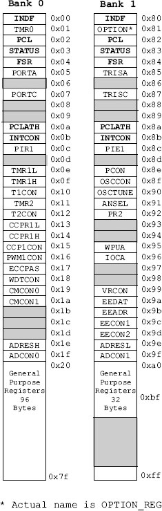
Figure 7-6 16F684 File Register Map.
The instruction set of most processors, including the PICs, provides a mechanism for accessing memory operands indirectly. Indirect addressing is based on the following capabilities:
• The address of a memory operand is loaded into a register. This register is called the pointer.
• The pointer register is then used to indirectly access the memory location at the address it “points to.”
• The value in the pointer register can be modified (usually incremented or decremented) so as to allow access to other memory operands.
In the PIC architecture, indirect addressing is implemented using two registers: INDF and FSR. The INDF register, always located at memory address 0x00 and mirrored in all banks, is not a physical register; therefore it cannot be directly accessed by code. The FSR register is the pointer register that is initialized to the address of a memory operand. Once a memory address is placed in FSR, any action on the INDF register takes place at the memory location pointed at by FSR. For example, if the FSR register is initialized to memory address 0x20, then clearing the INDF register has the effect of clearing the memory location at address 0x20. The action on the INDF register actually takes place at the address contained in the FSR register. Now if FSR (the pointer register) is incremented and INDF is again cleared, the memory location at address 0x21 will be cleared. Indirect addressing is covered in detail in the programming chapters later in the book.
7.3 Mid-Range I/O and Peripherals
Mid-range devices contain special modules to implement peripheral and I/O functions. The more complex the device, the more peripheral modules are likely to be present. For example, a simple mid-range PIC like the 16F84A contains few peripheral modules, specifically EEPROM data memory, I/O ports, and a timer module. The 16F87x PICs, on the other hand, in addition to I/O ports, EEPROM, and three individual timers, also have a parallel slave port, a capture and compare (PWM) module, a master synchronous serial port (MSSP) module, a universal asynchronous/synchronous receiver and transmitter (USART) module, and an analog-to-digital converter (A/D) module.
Other members of the mid-range family have additional or different peripheral and I/O modules. In the following sections we briefly describe the architecture of the most common peripheral modules. The programming details are covered in context elsewhere in the book.
Implementation of many different functions in a device with a small footprint requires multiplexing many of the PICs access connections. Figure 7-7 shows the pinout of the 16F84A and the 16F877 as well as the multiple functions of many pins in either device.

Figure 7-7 16F84A and 16F877 Pin Diagrams.
Ports provide PICs with access to the outside world and are mapped to physical pins on the device. In some mid-range PICs (see Figure 7-7), some pins used in I/O operations are multiplexed with alternate functions of peripheral modules. A pin ceases to be a port when a peripheral module function is activated for that pin.
General port pins are bi-directional; therefore they can be configured either as input or output. Each port has a corresponding TRIS register. The setting in this register determines if a port is designated as input or output. A value of 1 in the port’s TRIS register makes the port an input and a value of 0 makes the mapped port an output. Input ports are used in communicating with input devices, such as switches, keypads, and input data lines from hardware devices. Output ports are used in communicating with output devices, such as LEDs, Seven-Segment displays, liquid-crystal displays (LCDs), and data output line to hardware devices such as motors.
Although port pins are bit mapped, they are read and written as a unit. For example, the PORTA register holds the status of the eight pins possibly mapped to port A. Writing to a specific port writes to the port latches. Write operations to ports are actually read-modify-write operations. The port pins are first read, then the value is modified, and finally written to the port’s data latch. As previously mentioned, some of the port pins are multiplexed; for example, pin RA4 is multiplexed with the Timer0 module clock input; therefore, it is labeled RA4/T0CKI pin in the device’s pinout. Other PORTA pins are multiplexed with analog inputs and with other peripheral functions. The device data sheets contain information regarding the functions assigned to each device pin.
Timer modules are available in all mid-range PICs; in fact, the TIMER0 module is present in all PICs of the mid-range family. The TIMER0 module has the following features:
• 8-bit timer/counter
• Readable and writable
• 8-bit software programmable prescaler
• Internal or external clock select
• Interrupt on overflow from FFh to 00h
• Edge select for external clock
Chapter 11 is devoted entirely to the architecture and programming of timers and counters.
7.3.3 Capture and Compare Module
Some mid-range devices contain one or more capture and compare modules, designated as Capture/Compare/PWM. In Figure 7-7 you can see that one of the functions multiplexed onto pin 17 of the 16F877 is labeled CCP1 (Capture and ComPare module number 1). The CCP2 module is multiplexed onto pin number 16. The principal function of the capture and compare modules is to enhance timer operations. Each module contains the following elements:
A 16-bit register that can operate as a:
A 16-bit Capture register
A 16-bit Compare register
A PWM Master/Slave Duty Cycle register
When more than one capture and compare module is implemented in a single device, they are all identical in operation. In the 16F877 the two available modules are designated CCP1 and CCP2. In each module a Capture/Compare/PWM Register1 (CCPR1) is comprised of two 8-bit registers: CCPR1L (low byte) and CCPR1H (high byte). The CCP1CON register controls the operation of CCP1.
The CCP modules find use in recording events such as measuring time periods, counting, generating pulses and periodic waveforms, and voltage averaging.
7.3.4 Master Synchronus Serial Port
Some mid-range PICs come equipped with hardware modules to implement serial protocols, including SPI and I2C. The module that provides these interfaces is called the Master Synchronous Serial Port, or MSSP. The MSSP module can operate in either the slave or the master mode, as well as in a free bus mode, also called the multi-master function. The MSSP module is useful for communicating with other peripheral or microcontroller devices. The peripheral devices can be serial EEPROMs, shift registers, display drivers, or A/D converters, etc. The MSSP module is discussed in Chapter 14 in the context of EEPROM data memory programming.
The Universal Synchronous Asynchronous Receiver Transmitter (USART) module in the 16F87x family is also known as a Serial Communications Interface, or SCI. The USART module is used in communicating with devices and systems that support the RS-232 protocol, including computers and terminals. It can be configured as an asynchronous full-duplex device, as a synchronous half-duplex master, or as a synchronous half-duplex slave. In the synchronous mode, the USART is useful in communicating with analog-to-digital and digital-to-analog integrated circuits or for accessing serial EEPROMS. The USART is discussed extensively in the context of serial communications and programming EEPROMS. These topics are covered in Chapter 20 and Chapter 14, respectively.
Until recently A/D conversions required the use of dedicated devices, usually in the form of an integrated circuit component. In Microchip documentation, the analog-to-digital conversions module is referred to as ADC. Some mid-range PICs now come with on-board A/D hardware. One of the advantages of using on-board A/D converters is saving interface lines. Interfacing with a hardware analog-to-digital IC usually requires three to four lines. A similar function can be implemented with on-board A/C hardware with a single line. This saving in I/O lines can be significant in many PIC circuits.
Mid-range PICs equipped with A/D converters have either 8- or 10-bit resolution and can receive analog input in 2 to 16 different channels. For example, the 16F877 contains eight analog input channels at a 10-bit resolution. A/D converters use a sample-and-hold capacitor to store the analog charge and perform a successive approximation algorithm to produce the digital result. When the converter resolution is 10 bits these are stored in two 8-bit registers, one of them having only four significant bits. The ADC module on the 16F684 PIC provides a 1-bit binary output from a single analog signal. The presence of this module is sometimes the reason for preferring the 16F684 over its 16F84 and 16F84A predecessors.
The A/D module has high- and low-voltage reference inputs that are selected by software. The module can operate while the processor is in SLEEP mode, but only if the A/D clock pulse is derived from its internal RC oscillator.
7.4 Mid-Range PIC Core Features
Core features refer to those that apply to all members of the mid-range family. It includes the following elements:
• The device oscillator
• The reset mechanism
• CPU architecture and operation
• The ALU
• Data memory organization
• The interrupt system
• The instruction set
We have already discussed the architecture and general features of the CPU and the ALU, as well as to data memory organization. The remaining topics (oscillator, reset, interrupts, and instruction set) are covered in the following sub-sections.
Mid-range PICs require a clock signal for its operation. The clock signal source can be external to the PIC or an internal oscillator. Different mid-range PICs support different numbers of oscillator modes. For example, the 16F877 and the 16F684 can execute in any one of eight modes, but in the 16F84 only four oscillator modes are available. The 16F684 has eight possible clock modes, two of which originate in an internal oscillator.
The oscillator mode is selected at device programming time and cannot be changed at runtime. The configuration bits, which are nonvolatile flags set during device programming, determine which oscillator mode is used by the program, according to those supported by the device. Some mid-range PICs (like the 16F684) support unique oscillator modes that are not generally found in other members of the mid-range family. The following are the most common mid-range oscillator modes:
1. LP, low frequency crystal
2. XT, crystal resonator
3. HS, high speed crystal resonator
4. RC, external resistor/capacitor
5. EXTRC, external resistor/capacitor
6. EXTRC, external resistor/capacitor with CLKOUT
7. INTRC, internal 4-MHz resistor/capacitor
8. INTRC, internal 4-MHz resistor/capacitor with CLKOUT
The resistor/capacitor oscillator option is the cheapest to implement but also the least accurate one. This option should be used only in systems where clock accuracy and consistency are not issues. The low-frequency crystal option is the one with the lowest power consumption and is suitable for systems where power consumption is an important factor.
The first three oscillator modes (LP, XT, and HS) allow selecting different frequency ranges. The HS has the highest frequency range and consumes the most power. The XT option is based on a standard crystal resonator and has mid-range power consumption. The LP option has low gain and consumes the least power of the three crystal modes. The general rule is to use the oscillator with the lowest possible gain that still meets the circuit requirements. The RC mode with EXTRC and CLKOUT features have the same functionality as the straight RC oscillator option.
The XT option (crystal resonator) can be provided in a convenient ceramic package. This device, called a ceramic resonator, contains three pins. The ones on the extremes are connected to the corresponding oscillator input lines on the PIC, labeled OSC1 and OSC2. The center pin is connected to ground. Figure 7-8 shows the circuit diagram for an oscillator and a crystal resonator.
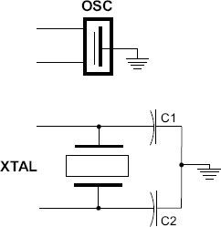
Figure 7-8 Circuit Diagrams for a Ceramic Resonator and a Crystal Oscillator.
Alternatively, the oscillator function can be provided by an integrated circuit (such as the ICS502) that can generate several different clock frequencies. Some circuits, especially in PIC demonstration boards, contain jumper pins that allow selecting among several clock rates.
The reset mechanism is used to place the PIC in a known condition, to gain control of a run-away or hung-up program, as a forced interrupt in program execution, or to make the device ready at program load time. The processor’s !MCLR pin produces the reset action when it reads logic zero. The exclamation sign preceding the pin’s name (or alternatively, as a line over the text) indicates that the action is active-low. To prevent accidental resets the !MCLR pin must be connected to the positive voltage supply through a 5K or 10K resistor. When a resistor serves to place a logic 1 on a line, it is called a pull-up resistor.
The mid-range PICs are capable of several reset actions:
• Reset during power on (POR)
• !MCLR reset during normal operation
• Reset during SLEEP mode
• Watchdog timer reset (WDT)
• Brown-out reset (BOR)
• Parity error reset
The most common reset sources are the first two in the preceding list. POR reset serves to bring all PIC registers to an initial state, including the program counter register. This action is taken automatically by the microcontroller. The second source of a reset action takes place when the !MCLR line is intentionally brought down, usually by the action of a pushbutton reset switch. This switch is useful during program development because it provides a way of forcefully re-starting execution. Figure 7-9 shows a typical wiring of the !MCLR line to provide a reset activated by a pushbutton switch. The circuit includes an LED that lights up when the power is on.

Figure 7-9 Typical Wiring of the Reset Switch.
User RAM memory is not affected by a reset. The PICs general-purpose registers (GPRs are in an unknown state during power up and are not changed by reset). SFR registers, on the other hand, are reset to an initial state. The initialization conditions for each of the SFRs can be found in the device data sheet. The most important of these is perhaps the program counter (PC), which is reset to zero. This action directs execution to the first instruction, effectively restarting the program.
During power-up, the processor itself initiates a reset when the power supply voltage goes from 1.2 to 1.8V. Several bits in various registers are related to the reset action, but these are not available in all mid-range devices. For example, some high-end devices in the mid-range group, such as the 16F87x, contain two bits in the PCON register that are reset related. One of them (named !POR) allows determining the power-on reset status. The other one (named !BOR) informs about the brown-out reset status. However, the PCON register does not exist in the 16F84 or 16F84A.
The interrupt mechanism provides a way of having the microcontroller respond to events as they occur, rather than being forced to poll devices in order to determine their state. The interrupt is said to work like a “tap on the shoulder" of the microcontroller, calling its attention to an event that requires an action or device that needs servicing. After responding to or ignoring the interrupt, the CPU resumes processing where it left off.
In computer technologies the interrupt mechanism is a complicated hardware/software system that often includes a programmable interrupt controller. Processors and microprocessors usually support hardware and software interrupts and maskable and nonmaskable interrupts, which can originate in practically any device connected to the system. In PICs, the interrupt mechanism is much simpler and varies considerably even among members of the same PIC family.
All PICs of the mid-range family support interrupts to some degree. The interrupt source usually originates in one of the hardware modules, although some sources can generate more than one interrupt. For example, the 16F684 supports eleven interrupt sources. The following are common interrupt sources in the mid-range family, although not all are supported by every PIC.
• INT pin interrupt (external interrupt)
• TMR0 overflow interrupt
• PORTX change interrupt
• Comparator change interrupt
• Parallel slave port interrupt
• USART interrupts
• Receive and transmit interrupt
• A/D conversion complete interrupt
• LCD interrupt
• Data EEPROM write complete interrupt
• Timer overflow interrupts
• CCP interrupt
• SSP interrupt
Several SFRs are related to the interrupt systems. The INTCON register provides interrupt enabling and control, and the PIE1, PIE2, PIR1, and PIR2 registers have specific device-related functions. Programming interrupts are discussed in the context of the corresponding operations later in this book.
The mid-range PIC instruction set consists of 35 instructions, divided into three general groups:
• Byte-oriented and byte-wise file register operations
• Bit-oriented and bit-wise file register operations
• Literal and control instructions
Table 7.1 lists and briefly describes each instruction in the mid-range set.
Table 7.1
Mid-Range PIC Instruction Set


7.5.1 STATUS and OPTION Registers
The STATUS register is one of the SFRs in mid-range PICs. The bits in this register reflect the arithmetic status of the ALU, the RESET status, and the bits that select which memory bank is currently being accessed. Because the bank selection bits are in the STATUS register, it must be present and at the same relative position in every bank. Figure 7-10 is a bitmap of the STATUS register.
The STATUS register can be the destination for any instruction. If it is, and the Z, DC, or C bits are affected, then the write operation to these bits is disabled. In addition, the TO and PD bits are not writable. Some instructions may have an unexpected action on the STATUS register bits; for example, the instruction
clrf STATUS
clears the upper 3 bits, sets the Z bit, and leaves all other bits unchanged. For this reason it is recommended that only instructions that do not change the Z, C, and DC bits be used to alter the STATUS register. The only ones that qualify are BCF, BSF, SWAPF, and MOVWF.
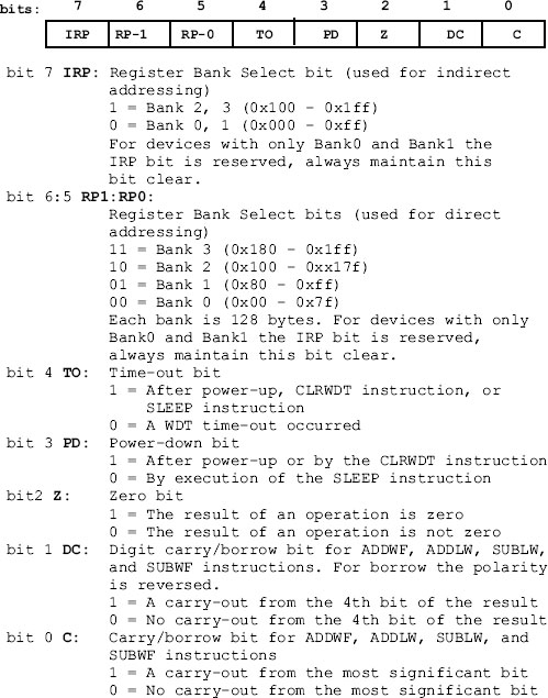
Figure 7-10 STATUS Register Bitmap.
The OPTION register is actually named the OPTION_REG to avoid a name clash with the option instruction. The OPTION_REG register contains several bits related to interrupts, the internal timers, and the Watchdog timer. Figure 7-11, on the following page, is a bitmap of the OPTION_REG register.

Figure 7-11 Bitmap of the OPTION_REG Register.
EEPROM (pronounced double-e PROM or e squared PROM) stands for Electrically-Erasable Programmable Read-Only Memory. EEPROM memory is used in computers and digital devices as nonvolatile storage. EEPROM is not RAM, as RAM memory is volatile and EEPROM retains its data after power is removed. EEPROM memory is found in USB flash drives and in the nonvolatile storage of several microcontrollers, including many PICs.
The one advantage of EEPROM memory is that it can be erased and written electronically, without removing the chip. The predecessor technology, named EPROM, required that the chip be removed from the circuit and placed under ultraviolet light. EEPROM simplifies the erasing and rewriting process. In the PIC architecture, EEPROM data memory refers to both on-board EEPROM memory and to EEPROM memory ICs as separate circuit components. In general, EEPROM elements are classified according to their electrical interfaces into serial and parallel. Most EEPROM memories used in PICs are serial EEPROMs, also called SEEPROMs. The typical use of serial EEPROM on-board memory and EEPROM on ICs is in the storage of passwords, codes, configuration settings, and other information to be remembered after the system is turned off. For example, a PIC-based security system can use EEPROM memory to store the system password. Because EEPROM can be written, the user can change this password and the new one will also be remembered.
7.6.1 EEPROM in Mid-Range PICs
The mid-range PICs are equipped with EEPROM memory in three possible sizes: 64 bytes, 128 bytes, and 256 bytes. EEPROM memory allows read and write operations. This memory is not mapped into the processor’s data or program area, but in a separate block that is addressed through some SFRs. The registers related to EEPROM operations are
• EECON1
• EECON2 (not a physically implemented register)
• EEDAT
• EEADR
EECON1 contains the control bits, and EECON2 is used to initiate the EEPROM read and write operations. The 8-bit data item to be written must first be stored in the EEDATA register, while the address of the location in EEPROM memory is stored in the EEADR register. The EEPROM address space always starts at 0×00 and extends linearly to maximum in the device.
When a write operation is performed, the contents of the EEPROM location is automatically erased. The EEPROM memory used in PICs is rated for high erase/write cycles. EEPROM programming is the topic of Chapter 14.