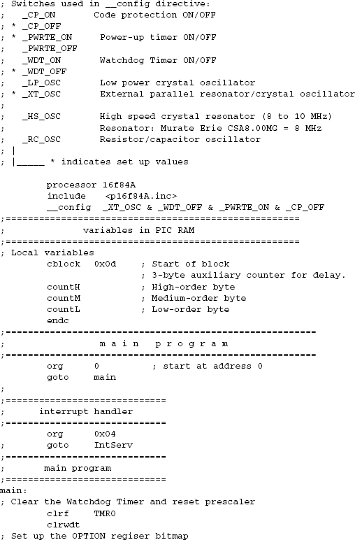
11.1 Controlling the Time Lapse
The mid-range PICs contain facilities and devices for controlling and manipulating time lapses in a program; these are usually in the form of timing and counting operations. It is difficult to find a PIC application that does not require some form of counting or timing. In the programs previously developed we have used a simple iteration counter that produces a delay by means of a loop that implements a delay by wasting a series of machine cycles. In this chapter we expand the theory and the use of delay loops, and explore the use of the built-in timing and counting circuits on the 16F84. The material presented relates to Chapter 10 because timing and counting operations can be set up to generate interrupts. The interrupt-based sample programs developed in this chapter can be executed and tested in Demo Board I described in Chapter 10.
The basic timer facility on the 16F84 PIC is known as the Timer0 module, as the free-running timer, as the timer/counter, or simply as TMR0. Timer0 is an internal 8-bit register that increments automatically with every PIC instruction cycle until the count overflows the timer capacity, which takes place when the timer count goes from 0xff to 0x00. At that time the timer restarts the count.
The Timer0 module is in fact a peripheral device that adds a specific functionality to the microcontroller. Learning to program the Timer0 module serves as an introduction to programming PIC peripheral devices. There are few such devices in the 16F84 but other mid-range PICs (such as the 16F877 and the 16F684) contain other peripherals. These include several timers, capture/compare modules, various serial and parallel interfaces, USART and other communications hardware, comparators, and converters.
The 16F84 Timer0 module has the following characteristics:
• A timer register that is readable and writeable by software
• Can be powered by an external or internal clock
• Timing edge for external clock can be selected
• 8-bit software programmable prescaler
• Interrupt capability
• Can be used as a timer or as a counter
Figure 11-1 is a simplified block diagram of the Timer0 hardware.
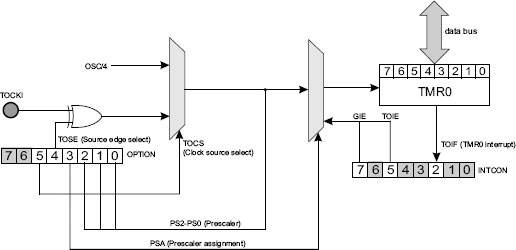
Figure 11-1 Timer0 Block Diagram.
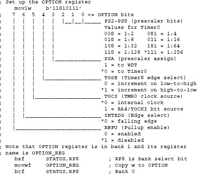
Block diagrams, such as the one in Figure 11-1, provide valuable and compact circuit information. In this example the block diagram, which is read left to right, shows that timer operation can be assigned to the internal clock (OSC/4 in the diagram) or to the PICs TOCKI pin that is shared with port RA4. Bit 5 of the OPTION register (labeled TOCS in the diagram) performs the selection. If TOCS is set, then the timer is linked to the RA4/TOCKI pin. In this mode the timer is used as a counter. If TOCS is reset, then the timer uses the PIC’s instruction cycle clock signal. The shaded trapezoids in the illustration depict multiplexer functions, sometimes called mux (see Section 5.5.1). Bits inside the multiplexer symbol show which input is selected by the TOCS bit.
If an external source is selected by setting the TOCS bit, then bit 4 of the OPTION register (labeled TOSE) allows selecting whether the timer increments on the high-to-low or low-to-high transition of the signal on the RA4/TOCKI pin. The XOR symbol with inputs from the TOCKI pin and bit 4 of the OPTION register indicate this action. If the TOSE bit is set, then increment takes place on the high-to-low transition of the TOCKI pin, as it corresponds with the logical XOR operation. Otherwise the increment takes place on the low-to-high transition of the TOCKI pin. The gray shading of bits 6 and 7 of the OPTION register (and of other register bits in the diagram) indicate that these bits are not used in configuring Timer0 operations.
The rightmost multiplexer symbol depicts the control of the prescaler function. The prescaler serves as a frequency divider for the signal and allows slowing down the clock action on Timer0. As shown in Figure 11-1, the control bit for the prescaler function is bit 3 of the OPTION register, labeled PSA. If this bit is clear, the prescaler is assigned to the Timer0 module. If the PSA bit is set, then the prescaler is assigned to the Watchdog timer. Bits 0, 1, and 2 of the OPTION register define eight possible prescaler settings.
The Timer0 module can be visualized as a register that increments with every instruction cycle at one-fourth the clock rate, that is, as a timer. In a PIC equipped with a 4-Mhz oscillator, the timer register increments at a rate of one pulse per millisecond without the prescaler. Because there are eight bits in the counter register, the value stored is in the range 0 to 255 decimal (shown as TMR0 in the block diagram of Figure 11-1). When the counter overflows, the register is reset. The prescaler allows slowing down this rate. The various settings of the prescaler bits of the OPTION register (bits 0, 1, and 2) allow selecting one of eight possible rate divisors (2, 4, 8, 16, 32, 64, 128, or 256)
PIC applications sometimes read the timer register (TMRO) directly. Alternatively, Timer0 can be set up to generate an interrupt at every transition from 0xff to 0x00, that is, every time the counter overflows. The timer register can be accessed in bank 0, offset 0x01. The timer interrupt is enabled by setting bit 5 (labeled TOIE) of the INTCON register. In this case the Global Interrupt Enable bit (labeled GIE) of the INTCON register must also be set. Once the timer interrupt is enabled, the Timer Interrupt Flag, assigned to bit 2 of the INTCON register (labeled TOIF) will be set on every overflow of the timer register. At that time an interrupt will take place. The TOIF bit (also called the Timer0 flag) must be cleared by the interrupt handler so that the timer interrupt can take place again. Later in this chapter we develop a sample program that uses Timer0 as an interrupt source.
We have seen that the counter prescaler consists of the three low-order bits in the OPTION register. These bits allow selecting eight possible values that serve as a divisor for the counter rate. When the prescaler is disabled, the counter rate is one- fourth the processor’s clock speed. If the prescaler is set to the maximum value (255) then one of 255 clock signals actually reach the timer. Table 11.1 shows the prescaler settings and their action on the rate of the Timer0 module.
Note that the prescaler can be assigned to either Timer0 or the Watchdog timer, but not to both. If bit 3 of the OPTION register is set, then the prescaler is assigned to the Watchdog timer. If it is clear it, is assigned to the Timer0 module.
Table 11.1
Prescaled Bits Selected Rates
|
|
|
|
|
|
000 |
0x00 |
1:2 |
001 |
0x01 |
1:4 |
010 |
0x02 |
1:8 |
011 |
0x03 |
1:16 |
100 |
0x04 |
1:32 |
101 |
0x05 |
1:64 |
110 |
0x06 |
1:128 |
111 |
0x07 |
1:256 |
The simplest application of the Timer0 module is to count instruction cycles in a simple delay loop. Applications in which the Timer0 register is polled directly are said to use a free running timer. There are two advantage in free running timers over conventional delay loops: the prescaler provides a way of slowing down the count, and the delay is independent of the number of machine cycles in the loop body. In most cases this means that it is easier to implement an accurate time delay using the Timer0 module than by counting instruction cycles. The drawback is that Timer0 must first be set up for this mode of operation.
Calculating the time taken by each counter iteration requires that we first divide the clock speed by four to obtain the instruction speed. We know that a PIC running on a 4-MHz oscillator clock increments the counter every 1 MHz. If the prescaler is not used, the counter register is incremented at a rate of 1 µs, which is the same as saying that the Timer0 clock beats at a rate of 1,000,000 cycles per second. If the prescaler is set to the maximum divisor value (256), then each increment of the timer takes place at a rate of 1,000,000/256 µs, which is approximately 3,906 µs or 3.906 ms. Because this is the slowest possible rate of the timer in a machine running at 4 MHz, it is often necessary to employ supplementary counters in order to achieve longer delays.
The fact that the timer register (TMR0) is both readable and writeable makes possible some interesting timing techniques. For example, an application can set the timer register to an initial value and then count up until the timer overflows or a predetermined limit is reached. If the difference between the limit and the initial value is, let’s say, 100, then the routine will count 100 times the timer rate per beat instead of 256.
Two simple elements can be used in designing a timing routine with a specific delay: the number of timer iterations counted by the Timer0 hardware and the prescaler assignment. Suppose there is a routine that allows Timer0 to start from zero and count up. In this case when the count reaches the maximum value (0xff), the routine would have introduced a delay of 256 times the Timer0 clock rate. In this case a prescaler assignment can be used to further reduce the number of clock beats read by the timer. If we select the maximum value for the prescaler (assuming a machine clock of 4 MHz) then each timer beat will take place at a rate of 1,000,000/256, or approximately 3,906 timer beats per second. Because in this example the routine reads the maximum number of iterations in the counter register (256), the delay can be calculated by dividing the number of beats per second (3,906) by the number of counts in the delay loop. In this case 3,906/256 results in a delay of approximately 15.26 iterations per second.
A general formula for calculating the number of timer beats per second is as follows:
where T is the number of clock beats per second, C is the system clock speed in Hz, P is the value stored in the prescaler, and R is the number of iteration counted in the TMR0 register. The range of both P and R in this formula is from 1 to 256. Also notice that the reciprocal of T (1/T) gives the time delay, in seconds, per iteration of the delay routine.
In the previous section we saw that even using the largest possible prescaler and counting the maximum number of timer beats, the longest possible timer delay in a 4MHz system is approximately of 1/15 of a second. Add to this that applications must sometimes devote the prescaler to the Watchdog timer, which impedes its use in Timer0. Without the prescaler the maximum delay is approximately 3,906 timer beats per second. Consequently, applications that must measure time in seconds (or in minutes, hours, or days) must find ways of keeping count of large number of repetitions of the timer beat.
In implementing counters for larger delays we must be careful not to introduce round-off errors. For instance, in the previous example, a timer cycles at the rate of 15.26 times per second. The closest integer to 15.25 is 15, so if we now set up a one-second counter by counting fifteen iterations, we would introduce an error of approximately 2%. Considering that (in the previous example) each iteration of the timer contains 256 individual beats, there are 3,906.25 individual timer beats per second at the maximum prescaled rate. If we were to implement a timer by keeping track of the individual prescaled beats (instead of timer iterations), the count would proceed from 0 to 3,906 instead of from 0 to 15. Approximating 3,906.25 by the closest integer, 3,906, introduces a much smaller round-off error than what results from approximating 15.26 with 15.
Finally, in this same example, we could eliminate the prescaler so that the timer beats at the clock rate, that is, at 1,000,000 beats per second. In this option a counter that counts from 0 to 1,000,000 would have no intrinsic error due to round-off.
Which solution is more adequate depends on the accuracy required by the application and the resulting complexity of the code. A timer counter in the range 0 to 15 can be implemented in a single 8-bit register. A counter in the range 0 to 3,906 requires two bytes. One to count from 0 to 1,000,000 requires three bytes. Because arithmetic operations in the 16F84 are 8-bits, manipulating multiple-register counters requires more complicated processing.
The actual implementation of a delay routine based on multi-byte counters presents some difficulties. If the timer register (TMR0) is used to keep track of timer beats, then detecting the end of the count presents a subtle problem. Intuitively thinking, our program could detect timer overflow by reading the value in TMR0 and testing the zero flag in the status register. Because the movf instruction affects the zero flag, one could be tempted to code:
wait:
movf tmr0,w ; Timer value into w
btfss status,z ; Was it zero?
goto wait
; If this point is reached tmr0 has overflowed
But there is a problem: the timer ticks as each instruction executes. Because the goto instruction takes two machine cycles, it is possible that the timer overflows while the goto instruction is in progress; therefore the overflow condition would not be detected. A solution to this problem proposed in the Microchip documentation is to check for less than a nominal value by testing the carry flag, as follows:
wait1:
movlw 0x03 ; 3 to w
subwf tmr0,w ; Subtract w - tmr0
btfsc status,c ; Test carry
goto wait1
One adjustment that is sometimes necessary in free running timers results from the fact that when the TMR0 register is written, the count is inhibited for the following two instruction cycles. Software can usually compensate for this by writing an adjusted value to the timer register. If the prescaler is assigned to Timer0, then a write operation to the timer register determines that the timer will not increment for four clock cycles.
A more elegant and accurate solution has been described by Roman Black in a Web article titled “Zero-error One Second Timer”. Black credits Bob Ammerman with the suggestion of using Bresenham’s algorithm for creating accurate PIC timer periods. In the Black-Ammerman method the counter works in the background, either by polling or Interrupt-Driven. So the program can continue executing while the counter runs. In either case the timer count value is stored in a 3-byte register that is decremented by the software. The Internet article offers through coverage of this algorithm.
Timer0 operations can be assigned to the PIC RA4/TOCKI pin by setting bit 5 of the OPTION register (labeled TOCS). This mode is referred to as the counter mode. When the timer is setup to work as a counter, then bit 4 of the OPTION register (labeled TOSE) allows selecting whether the counter increments on the high-to-low or low-to-high transition of the signal.
When an external clock input is present in the RA4/TOCKI pin, the code must meet certain requirements in order to ensure that the external source can be synchronized with the internal clock. When no prescaler is used, the external clock input must be high and low for at least twice the internal clock rate. In addition, there must be a resistor-capacitor induced delay of 20 ns on both the high and low cycles. When a prescaler is used, the external clock input must be high and low for at least four times the rate of the internal clock rate. In addition, there must be a resistor-capacitor induced delay of 40 ns on both the high and low cycles.
Once the counter mode is enabled, any pulse on pin RA4/TOCKI is automatically counted in the TMR0 register. The mechanism can be compared to an automatic interrupt because no program action is required to keep track of the number of pulses. The routine can be coded so that when the timer count overflows an interrupt is generated. The interrupt handler can then increment a supplementary counter so that events that exceed 256 pulses can be recorded.
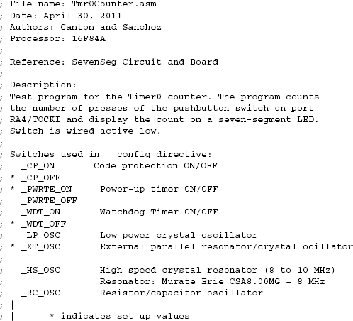
The program named TMR0Counter developed later in this chapter and contained in this book’s online software is an example of using the counter function of the Timer0 module.
Software routines that use the Timer0 module range in complexity from simple delay loops to configurable, Interrupt-Driven counters that must meet high timing accuracy requirements. When the time period to be measured does not exceed the one that can be obtained with the prescaler and the timer register count, then the coding is straightforward and the processing is uncomplicated. But often this is not the case. The following elements should be examined before attempting to design and code a Timer0-based routine:
1. What is the required accuracy of the timer delay?
2. Can the prescaler be used, or is the prescaler devoted to the Watchdog timer?
3. Does the program suspend execution while the delay is in progress, or does the application continue executing in the foreground?
4. Can the timer be Interrupt-Driven, or must it be polled?
5. Will the delay be the same on all calls to the timer routine, or must the routine provide delays of different magnitudes?
6. How long must the delay last?
In this section we explore several timer routines of different complexity and meeting various constraints. The first one uses the Timer0 module as a counter, as described in Section 11.3. Later we develop a simple delay loop that uses the Timer0 register instead of an instruction count. We conclude with an Interrupt-Driven timer routine that can be changed to implement different delays.
The 16F84 can be programmed so that port RA4/TOCKI is used to count events or pulses. This is accomplished by initializing the Timer0 module as a counter. If interrupts are not used, the process requires the following preparatory steps:
1. Port A, line 4, (RA4/TOCKI) is defined for input.
2. The Timer0 register (TMR0) is cleared.
3. The Watchdog timer internal register is cleared by means of the CLRWDT instruction.
4. The OPTION register bits PSA and PSO:PS2 are initialized if the prescaler is to be used.
5. The OPTION register bit TOSE is set so as to increment the count on the high-to-low transition of the port pin if the port source is active low. Otherwise the bit is cleared.
6. The OPTION register bit TOCS is set to select action on the RA4/TOCKI pin.
Once the timer is set up as a counter, any pulse received on the RA4/TOCKI pin (as long as it meets the restrictions mentioned in Section 11.3) is counted in the TMR0 register. Software can read and write to the TMR0 register, located at address 0x01 in bank 0, in order to obtain or change the event count. If the timer interrupt is enabled when the timer is defined as a counter, the interrupt takes place every time the counter overflows, that is, when the count cycles from 0xff to 0x00.
The circuit shown in Figure 11-2 contains a pushbutton switch wired to port RA4/TOCKI and a Seven-Segment LED display wired to port B lines 0 to 6.

Figure 11-2 Test Circuit for Timer/Counter Program.
Note that the circuit in Figure 11-2 is a section of the one used by Virtual Board A (in Figure 9.7). Programs that execute in the circuit of Figure 11-2 will also run in Virtual Board A.
The program named TimerCounter in this book’s online software package uses the circuit in Figure 11-2 (and in Virtual Board A) to demonstrate the programming of the Timer0 module in the counter mode. The program detects and counts action on the pushbutton switch wired to port RA4/TOCKI. The count (in hex digits in the range 0x00 to 0x0f) is displayed in the Seven-Segment LED connected to port B. When using Virtual Board A to demonstrate the program, make sure that toggle switch J1 is closed at the time the program executes. The programming of Seven-Segment LEDs was discussed in Chapter 9.
Code first clears the TMR0 register and the Watchdog timer, as follows:
main:
; Clear the timer and the Watchdog
clrf TMR0
clrwdt
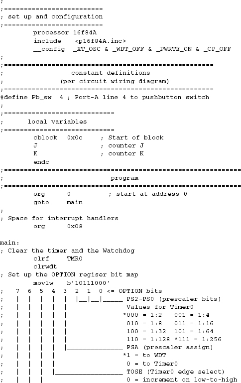
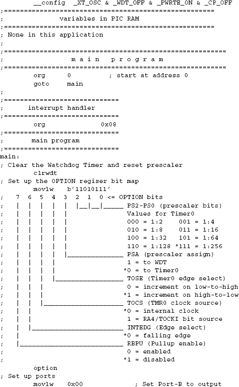
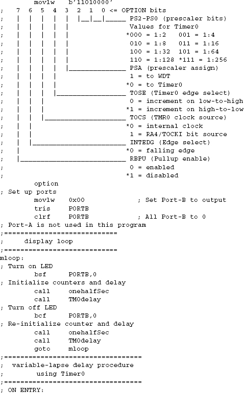
Next, the OPTION register must be set up as follows:
• Disable the prescaler (accomplished by setting the PSA bit that assigns it to the Watch dog timer).
• Set the Timer0 edge select bit (TOSE) to increment in the high-to-low signal transition.
• Select the RA4/TOCKI pin as a beat source.
The bits of the OPTION register that are not meaningful for this mode of Timer0 operation are set to their default state, as follows:

Now port B must be “trissed” for output and port A for input. Port B is also cleared:
At this point, every time the pushbutton switch wired to port A, line RA4/TOCKI, is pressed, one is added to the value in TMR0. Because the value to be displayed in the Seven-Segment LED goes from 0 to 0xf, the value in TMR0 must be scaled to this range. This is easily accomplished by masking off the four high-order bits of TMR0 at display time. Note that a binary counter is reminiscent of the odometer in an automobile, that is, the count proceeds from the lower digits to the higher ones. Therefore masking off a series of higher-order digits does not affect the count kept in the lower-order digits. More clearly, if you were to place a piece of tape over the three high-order digits of a car’s odometer, the value in the uncovered digits would continue to be correct. Code reads the value in TMR0 into w, masks off the four high-order bits, displays the resulting value, and loops back endlessly, as follows:

11.4.2 Timer0 as a Delay Timer
Another simple use of the Timer0 module is to implement a delay loop. In this application the Timer0 module is initialized to use the internal clock by setting the TOSE bit of the OPTION register. If the prescaler is to be used, as is often the case, the PSA bit is cleared and the desired pre-scaling is entered in bits PS2 to PS0 of the OPTION register.
The circuit in Figure 11-3 allows testing several timer-related programs developed in this chapter. Notice that this circuit is a section of the one for Virtual Board A in Figure 9.7; therefore applications developed for this circuit will also run in the Virtual Board A program.
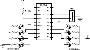
Figure 11-3 Circuit for Testing Several Timer Programs.
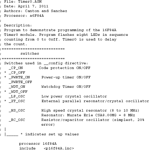
The program named DelayTimer, in this book’s online software package, uses a timer-based delay loop to flash eight LEDs displaying a binary value from 0x00 to 0xff. The delay routine executes in the foreground, so that processing is suspended while the count is in progress.
Code first clears the Watchdog timer:
; Clear the Watchdog timer and reset prescaler
clrwdt
The prescaler is assigned to Timer0 by clearing the PSA bit, and bits PS2 to PS0 are set to assign a 1:256 prescaler to the timer. The bits of the OPTION register that are not meaningful for this mode of Timer0 operation are set to their default state. Code is as follows:
Port B is then “trissed” for output and cleared. Because the program does not use port A, it is ignored by the code.
; Setup ports
movlw 0x00 ; Set port B to output
tris portb
clrf portb ; All port B to 0
The program’s main loop consists of adding one to the value in port B so as to bump the count. The delay routine named TM0delay is then called, followed by a goto instruction to the loop start.
mloop:
incf portb,f ; Add 1 to register value
call TM0delay
goto mloop
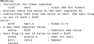
The delay procedure named TM0delay provides the necessary time lapse between successive increments in the count displayed. First the TMR0 register is cleared to make sure the timing starts correctly. Then the value in TMR0 is read into the w register and the constant 0xff is subtracted from W. When the count reaches 0xff, this subtraction sets the zero flag. Until that happens, code loops to a label named cycle. The routine returns to the caller when the time lapses.
A time-lapse routine can be designed so it can be modified (or reconfigured at call time) to produce a specific delay. This adjustable time-lapse procedure can be a useful tool in any programmer’s library. In previous sections we have developed delay routines that do so by counting timer pulses. This same idea can be used to develop routines that can be adjusted so as to produce accurate delays within a range by modifying the value of the count.
The routine itself can be implemented to varying degrees of sophistication. One variation is a procedure that receives the desired time lapse as a parameter. Another one is a procedure that reads the desired time lapse from program constants, which can be edited at assembly time. A third option, used by the program VariLapse in this book’s software package, uses three variables to hold the number of machine cycles in the desired wait period. By using machine cycles instead of time units (such as microseconds or milliseconds), the procedure becomes adaptable to devices running at different clock speeds. Because each instruction (or Timer0 iteration) requires four clock cycles, the device’s clock speed in Hz is divided by four in order to determine the number of machine cycles per time unit.
For example, a processor equipped with an 8-MHz clock executes at a rate of 8,000,000/4 machine cycles per second, that is, 2,000,000 instruction cycles per second. To produce a one-quarter second delay requires a wait period of 2,000,000/4 or 500,000 instruction cycles. By the same token, a 16F84 running at 4 MHz executes 1,000,000 instructions per second. In this case, a one-quarter second delay would require waiting 250,000 instruction cycles.
11.4.5 Variable Lapse Timer Program
The program titled VariLapse in this book’s software package uses Timer0 to produce a variable-lapse delay. The delay is calculated based on the number of machine cycles necessary for the desired wait period, as described in the preceding paragraph. The program uses the Black-Ammerman methods described earlier in this chapter, which require a prescaler of 1:2 so that each timer iteration takes place at one-half the clock rate.
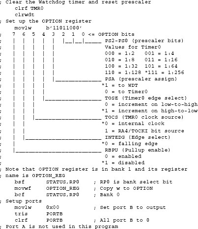
The program first initializes the OPTION register in order to achieve the following setup:
• The prescaler is assigned to Timer0 (PSA bit) and a 1:2 rate is selected in OPTION_REG bits 0 to 2.
• The internal clock is selected as a timing source (TOCS bit).
• Timing count is set to increment in the high-to-low signal transition (TOSE bit).
• OPTION register bits not used by the program are set to their default values.
• Next, port B is selected for output and cleared. Port A is ignored by the code because it is not used by the program.
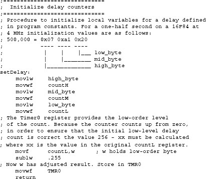
The VariLapse program requires a one-half second delay and assumes a 16F84 running at 4 MHz. The delay procedure must wait for 500,000 clock beats to take place before returning to the caller. The value 500,000 requires three storage bytes. This is easily seen by converting 500,000 to hexadecimal: 500,000 = 0x07a120. At this point a simple decimal-to-hex calculator would be convenient. Several screen-based hex calculators (including a screen version of the HP 16C) are available free on the Internet. The program defines the hex equivalent of 500,000 in three constants:

The advantage of using equ directives in defining these values is that they can easily be edited in order to accommodate a different processor speed or to change the delay. In the sample program we coded a procedure called setDelay, which initializes three counter variables using the values contained in the constants low_byte, mid_byte, and high_byte. The setDelay procedure is coded as follows:

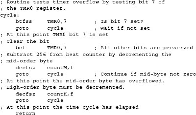
The logic for a 3-byte counter consists of decrementing the low-order counter until it expires, then the mid-order counter, and when it goes to zero the high-order counter is decremented. If the high-order counter expires, the delay concludes. The flowchart in Figure 11-4 shows this sequence of operations.
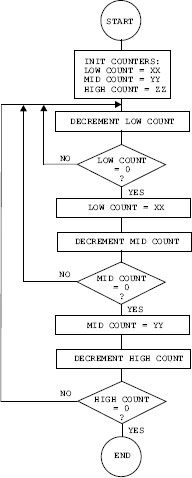
Figure 11-4 Multiple Counter Flowchart.
Roman Black points out in his Web article (mentioned earlier in this chapter) that one of the difficulties of timing routines based on counters is that the exact count is lost by the manipulations necessary to detect the end of each counter iteration. One possible solution is to use interrupts to detect the end of the count. Another one (proposed by Black) is based on introducing a 1:2 delay in the timer by means of the prescaler. Because the prescaled timer beats at one-half the instruction rate, 128 timer cycles will be required for one complete iteration at the full instruction rate. This allows us to test the state of the counter’s high-order bit to detect when the count has expired. A new count can be started by clearing this high-order bit without affecting the validity of the count held in the remaining seven bits. The result is a timer-counter that does not lose step while detecting the end of each iteration level.
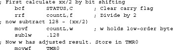
The delay routine uses the Timer0 register to provide the low-order level of the count. Because the counter counts up from zero, in order to ensure that the initial low-level delay count is correct, the value 128 - (xx/2) must be calculated, where xx is the value in the original countL register. The program performs the division by 2 by shifting bits to the right one position. The resulting value is subtracted from 128 and the result stored in TMR0, as follows:
The delay routine detects timer overflow by testing bit 7 of the TMR0 register. If the bit is set, then 256 time cycles have elapsed (except in the first iteration) and the mid-order counter register is decremented. If the mid-order register overflows when it is decremented, then the high-order register is decremented. If it overflows, the counter has gone to zero and the delay routine ends, as follows:
The circuit in Figure 11-3 and the Virtual Board A application can be used to test the VariLapse program.
Interrupt-driven timers and counters have two major advantages over polled routines:
1. The time lapse counting take place in the background so that the application can continue to do other work in the foreground.
2. Processing can take place without the prescaler, which can be used for the Watchdog timer.
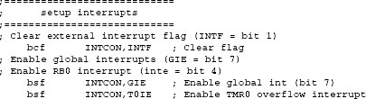
Developing a timer routine that is Interrupt-driven is quite similar to developing any other interrupt routines. The initialization consists of configuring the OPTION and the INTCON register bits for the task at hand. In the particular case of an Interrupt-Driven timer, the following are necessary:
1. The external interrupt flag (INTF in the INTCON Register) must be initially cleared.
2. Global interrupts must be enabled by setting the GIE bit in the INTCON reg ister.
3. The Timer0 overflow interrupt must be enabled by setting the TOIE bit in the INTCON register.
The TimerInt program is an Interrupt-Driven version of the VariLapse program developed earlier. Here again, code uses Timer0 to produce a variable-lapse delay. The delay of one-fourth second is calculated based on the number of machine cycles necessary for the desired wait period.
In the TimerInt program the prescaler is not used with the timer, so the initialization code sets the PSA bit in the OPTION register so that the prescaler is assigned to the Watchdog timer. The following code fragment is from the TimerInt program:
Interrupts are set up clearing the INTF flag in the INTCON register and setting the GIE and TOIE bits.
As in the program VariLapse, developed previously in this chapter, the timer operates by decrementing a 3-byte counter that holds the number of timer beats required for the delay. In the case of the TimerInt program, the routine that initializes the register variables from the local constants (called setDelay) also makes the correction so that the initial value loaded into the TMR0 register is correctly adjusted. The code is as follows:
The interrupt service routine in the TimerInt program receives control when the TMR0 register underflows, that is, when the count goes from 0xff to 0x00. The service routine then proceeds to decrement the mid-range counter register and adjust, if necessary, the high-order counter. If the count goes to zero, the handler toggles the LED on port B, line 0, and reinitializes the counter variables by calling the setDelay procedure. The interrupt handler is coded as follows:

Note that one of the initial operations of the service routine is to clear the TOIF bit in the INTCON register. This action reenables the timer interrupt and prevents counting cycles from being lost. Because the interrupt is generated every 256 beats of the timer, there is no risk that by enabling the timer interrupt flag a re-entrant interrupt will take place.
The interrupt-based timer program named TimerInt can be tested on the circuit shown in Figure 11-3 or on Virtual Board A. Recall that Virtual Board I is used for interrupts that are based on port B input lines, which is not the case with the TimerInt program.
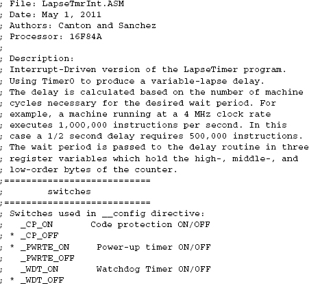
The 16F84 contains an independent timer with its own clock source called the WWatchdog timer or WDT. The purpose of the Watchdog timer is to provide a way for the processor to recover from a software error that impedes program continuation, such as an endless loop. The Watchdog timer is not designed to recover from hardware faults, such as a brown-out.
The Watchdog timer hardware is independent of the PIC’s internal clock. It has a time-out period from approximately 18 milliseconds to 2.3 seconds, depending on whether the prescaler is used. It is also not very accurate because it is sensitive to temperature. According to Microchip documentation, under worst case conditions its time-out period can take up to several seconds. The following program elements relate to Watchdog timer operation:
1. Configuration bit 2, labeled WDTE, enables and disables the Watchdog timer during system configuration. The WDT cannot be set or reset at runtime. It is enabled and disabled during programming.
2. The PSA bit in the OPTION register selects whether the prescaler is assigned to the Watch dog timer or to the Timer0 module.
3. Bits PS2 to PS0 in the OPTION register allow assigning eight rates to the Watchdog timer, from 1:1 to 1:128.
4. Bit 4 of the STATUS register, named the TO bit, is cleared when a time-out condition occurrs that originated in the WDT.
5. The power-down bit (PD) in the STATUS register is set after the execution of the clrwdt instruction.
6. The clrwdt instruction clears the Watchdog timer. It also clears the prescaler count (if the prescaler is assigned to the Watchdog timer) and sets STATUS bits TO and PD.
The purpose of the WDT is to provide a recovery mechanism for software errors. When the WDT timesout, the TO flag in the STATUS register is cleared and the program counter is reset to 0x000 so that the program restarts. Applications can prevent the reset by issuing the clrwdt instruction before the time-out period ends. When clrwdt executes, the WDT time-out period restarts.
11.5.1 Watchdog Timer Programming
Not much information is available regarding details of the operation or practical uses of the Watchdog timer in the 16F84. However, we can see that using the WDT in applications is not just a simple matter of restarting the counter with the clrwdt instruction. The timer is designed to detect software errors that can hangup a program, but how does it detect these errors and which conditions trigger the WDT operation is not clear from the information currently available. For example, an application that contains a long delay loop may determine that the Watchdog timer forces an untimely break out of the loop. The Watchdog timer provides a powerful error-recovery mechanism but its use requires careful consideration of program conditions that could make the timer malfunction.
The following programs demonstrate the programming discussed in this chapter: