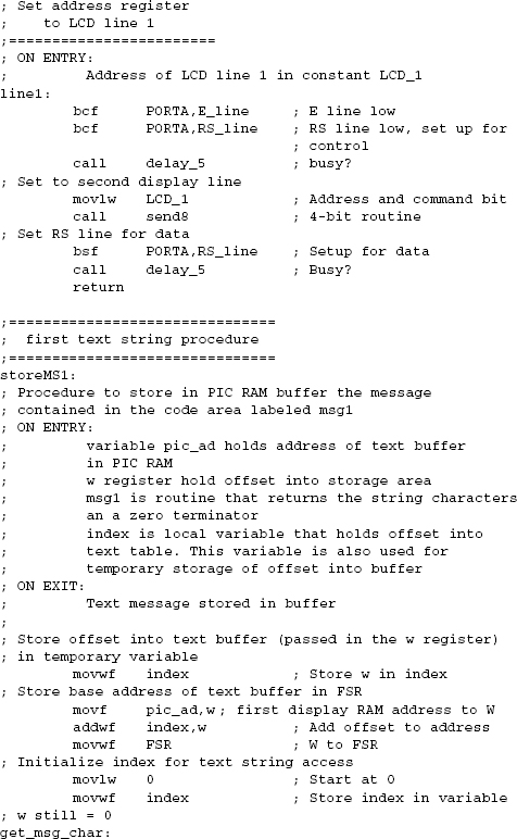
Analog-to-Digital and Real-Time Clocks
13.1 Clocks and the Digital Revolution
Digits are a human invention; nature does not count or measure using numbers. We measure natural forces and phenomena using digital representations, but the forces and phenomena themselves are continuous. Time, pressure, voltage, current, temperature, humidity, gravitational attraction; all exist as continuous entities that we measure in volts, pounds, hours, amperes, or degrees, so as to better understand them and to be able to perform numerical calculations.
In this sense, natural phenomena occur in analog quantities. Sometimes they are digitized so as to facilitate measurements and manipulations. For example, a potentiometer in an electrical circuit allows reducing the voltage level from the circuit maximum to ground, or zero level. In order to measure and control the action of the potentiometer, we need to quantify its action by producing a digital value within the physical range of the circuit; that is, we need to convert an analog quantity that varies continuously between 0 and 5 volts, to a discrete digital value range. If, in this case, the voltage range of the potentiometer is from 5 to 0 volts, we can digitize its action into a numeric range of 0 to 500 units, or measure the angle or rotation of the potentiometer disk in degrees from 0 to 180. The device that performs either conversion is called an A/D or analog-to-digital converter. The reverse process, digital-to-analog, is also necessary, although not as often as A/D. In this chapter we explore A/D conversions in PIC software and hardware.
The second topic of this chapter is the measurement of time in discrete (albeit, digital) units. In this context we speak of “real-time” as years, days, hours, minutes, and so on. So a real-time clock measures time in hours, minutes, and seconds, and a real-time calendar measures it in years, months, weeks, and days. Not all time units are in proportional relationship with one another. There are 60 seconds in a minute and 60 minutes in an hour, but 24 hours in a day, and 28, 29, 30, or 31 days in a month. Furthermore, the months and the days of the week have traditional names. Finally, the Gregorian calendar requires adding a twenty-ninth day to February on any year that is evenly divisible by 4. The device or software to perform all of these time calculations is referred to as a realtime clock. In this chapter we discuss the use of real-time clocks in PIC circuits.

Figure 13-1 A/D Converter Block Diagram.
In electronics, the typical A/D or ADC converter is a device that takes a voltage input and returns a binary digital number. Figure 13-1 is a block diagram of an A/D converter.
The electronic A/C converter requires an input in the form of an electrical voltage. Nonelectric quantities must be changed into a voltage level before the conversion can be performed. The device that performs this conversion is called a transducer. For example, a digital barometer must be equipped with a transducer that converts the measurement into voltage levels. The voltage levels can then be fed into an A/D converter and the result output in digital form.
An ideal A/D converter outputs into an infinite number of discrete steps that exactly represent the analog quantity. Needless to say, such a device cannot exist, and a real A/D converter must be limited to a numeric range. For example, the device in Figure 16-1 outputs a voltage range of 0 to +5 volts in four binary digits that represent values between 0 and 15. Another A/D converter may produce output in eight binary digits, and another in sixteen binary digits. The number of discrete values in the conversion is called the resolution. The converter’s resolution is usually expressed in bits. Figure 16-2 represents an A/C converter with a voltage range of 0 to +5 volts and a resolution of three bits.
Suppose that a value of 2.5 volts were input into the A/D converter in Figure 13-2. Because the output has a resolution in the range 0 to 7, the converter’s output would be either 4 or 5. The nonlinear characteristic of the output determines a quantization error that increases as the converter resolution decreases. Converters used in PIC circuits have a resolution of either 8, 10, or 12 bits. In each case the output range, or quantization level, is 0 to 255, 0 to 1023, or 0 to 4095. The voltage resolution of the converter is its maximum voltage range divided by the number of quantization levels. A device with a voltage range of 5 volts and a range of 255 levels has a voltage resolution of

Figure 13-2 ConverterQuantization Error.
The analog-to-digital converter performs accurately only if the input voltage is within the converter’s valid range. This range is usually selected by setting high and low voltage references on converter pins. For example, if +4 volts is input into the converter’s positive reference pin and +2 volts into the negative reference pin, then the converter’s voltage range lies between these values. In many PIC applications the converter range is selected as the system’s supply voltage and ground, that is, +5 and 0 volts. When a different range is externally referenced, there is a general restriction that the range cannot exceed the system’s positive and negative limits (Vdd and Vss). Also, a minimum difference is required between the high and low voltage references.
The output of the ADC is a digital representation of the original analog signal. In this context, the term quantization refers to subdividing a range into small but measurable increments. The quantization process can introduce a quantization error, which is similar to a rounding error.
The time required for the holding capacitor on the ADC to charge is called the acquisition time. The holding capacitor on the ADC must be given sufficient time to settle to the analog input voltage level before the actual conversion is initiated. Otherwise, the conversion is not accurate. The acquisition time is determined by the impedance of the internal multiplexer and that of the analog source. The exact acquisition time can be determined from the device’s data sheet, although 10K Ohms is the maximum recommended source impedance for 8- and 10-bit converters and 2.5K Ohms for 12-bit converters.
Most analog-to-digital converters in PIC applications, either internal or external, are of the successive approximation type. The successive approximation algorithm performs a conversion on one bit at a time, beginning with the most significant bit and ending with the least-significant bit. To determine each bit in the range, the value of the input signal is tested to see if it is in the upper or lower portion of this range. If in the upper portion, the conversion bit is a 1, otherwise it is a 0. The next most-significant bit is then tested in the lower half of the remaining range. The process is continued until the least-significant bit has been determined.
Several popular integrated circuits are used to perform as A/D converters, among them the ADC0831, the LTC1298, and the MAX 190 and MAX 191. The variations consist in the resolution and interfacing of the different ICs. Of these, the ADC0831, from National Semiconductor, is an 8-bit resolution, serial interface A/D quite suited to applications for small, mid-range PICs such as the 16F84. The input range of the 0831 is 0 to 5 volts, which matches the TTL voltage levels used in PIC circuits. The 0831 pin diagram is shown in Figure 13-3.
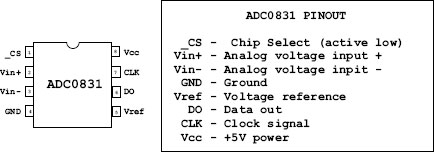
Figure 13-3 ADC0831 Pin Diagram.
The ADC0831 uses three control lines, labeled DO (data out), CLK (clock), and _CS (chip select) in Figure 13-3. Interfacing the ADC0831 requires three I/O lines. Of these, two can be multiplexed with other functions or with other ADC0831. Actually, only the chip-select (CS) pin requires a dedicated line. This allows for several ADCs to be multiplexed on the CLK and DO lines as long as each one has its own CS connection to the microcontroller. In this case, the controller determines which device is being read by the port to which its CS line is connected.
The input voltage range of the ADC0831 is determined by the Vref (positive voltage reference line) and Vin- (negative voltage reference line) pins. Vref is used to set the maximum level and Vin- the minimum. Because the ADC0831 has an 8-bit range, the voltage reading that matches the Vref value is read as 255 and the one that matches the Vin- value is read as 0. The minimum difference between the voltage limits is 1 volt.
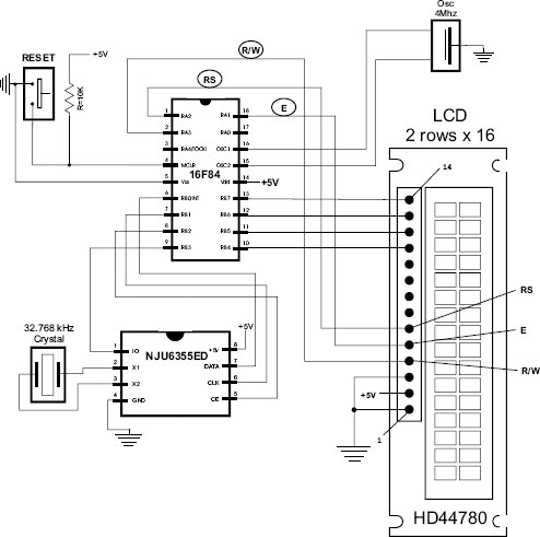
Figure 13-4 ADC0831 Demonstration Circuit.
13.3.1 ADC0331 Sample Circuit and Program
A simple circuit to illustrate the action of an analog-to-digital converter consists of connecting a potentiometer with the positive voltage reference line, as sown in Figure 13-4. In the circuit the potentiometer was selected so as to produce a voltage range between 0 and +5 volts. Vref was wired to the circuit’s +5V source and Vin- was wired to ground. The potentiometer variable line was connected to the ADC0831 Vin+ line and the other ADC lines to the corresponding 16F84 port B pins.
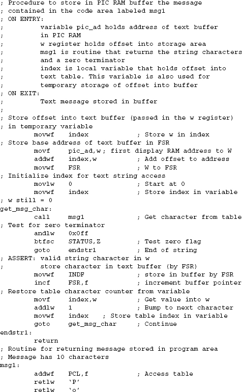
The sample program is called ADF84, and can be found in this book’s online software. The ADF84 program uses the ADC0831 to convert the analog voltage from the potentiometer, in the range +5 to 0 volts, into a digital value in the range 0 to 255. The value read is then displayed on the LCD. The initialization routine defines port-B, line 0 as input because this is the one connected to the DO line. The remaining lines in ports A and B are defined as output. ADC0831 processing consists of a single procedure that reads the analog line and returns an 8-bit digital value. The processing required is performed in the following steps:
1. The data return register (named rcvdata) is cleared and the bit counter register is initialized to count 8 bits.
2. The ADC0831 is prepared by bringing the CS line low and pulsing the CLK line.
3. The CLK line is pulsed and one bit is read from the low-order bit (DO line) of port B.
4. The bit is shifted into the data return register and the bit counter is decremented.
5. If the bit counter is exhausted, execution ends and the ADC is turned off. Otherwise processing continues at Step 3.
The following procedure, from the ADF84 program, reads digital data from the ADC0831:

A few years ago, A/D conversions always required the use of devices such as the ones described in the previous sections. Nowadays, many PIC microcontrollers come with onboard A/D hardware. One of the advantages of using onboard A/D converters is saving interface lines. The circuit shown in Figure 13-4 requires devoting three lines to the interface between the ADC0831 and the PIC 16F84. On the other hand, a similar circuit can be implemented in a PIC with internal A/C conversion by simply connecting the analog device to the corresponding PIC port. In the PIC world, where I/O lines are often in short supply, this advantage is not insignificant.
At the time of writing, PICs equipped with A/D converters have either 8- or 10-bit resolution and can receive analog input in two to sixteen different channels. The 16F877 with eight analog input channels at a 10-bit resolution is discussed. Nowadays, these PICs are easy to obtain. On the other hand, if the resolution required exceeds 10 bits, then the designer has to resort to an independent A/D IC, such as the LTC1298, which has a 12-bit resolution, or to others with even higher numbers of output bits.
13.4.1 A/D Module on the 16F87x
The PICs of the 16F87x family are equipped with an analog-to-digital converter module. The number of lines depends on the specific version of the device: 28-pin devices have five A/D lines and all others have eight lines. The converter uses a sample and hold capacitor to store the analog charge and performs a successive approximation algorithm to produce the digital result. The converter resolution is 10 bits, which are stored in two 8-bit registers. One of the registers has only four significant bits.
The A/D module has high- and low-voltage reference inputs that are selected by software. The module can operate while the processor is in SLEEP mode, but only if the A/D clock pulse is derived from its internal RC oscillator. The module contains four registers accessible to the application:
1. ADRESH - Result High Register
2. ADRESL - Result Low Register
3. ADCON0 - Control Register 0
4. ADCON1 - Control Register 1
Of these, it is the ADCON0 register that controls most of the operations of the A/C module. Port A pins RA0 to RA5 and port E pins RE0 to RE2 are multiplexed as analog input pins into the A/C module. In the 28-pin versions of the 16F87x, port pins RA0 to RA5 provide the five input channels. In all other implementations of the 16F87X, port E pins RE0 to RE2 provide the three additional channels.
Figure 13-5 shows the registers associated with A/D module operations.

Figure 13-5 Registers Related to A/C Module Operations.
The ADCON0 register is located in bank 0, at address 0x1f. Seven of the eight bits are meaningful in A/D control and status operations. Figure 13-6 is a bitmap of the ADCON0 register.
In Figure 13-6, bits 7 and 6, labeled ASCC1 and ADSC0, are the selection bits for the A/D conversion clock. The conversion time per bit is defined as TAD in PIC documentation. A/D conversion requires a minimum of 12 TAD in a 10-bit ADC. The source of the A/D conversion clock is software selected. The four possible options for TAD are:
1. Fosc/2
2. Fosc/8
3. Fosc/32
4. Internal A/D module RC oscillator (varies between 2 and 6 μs)
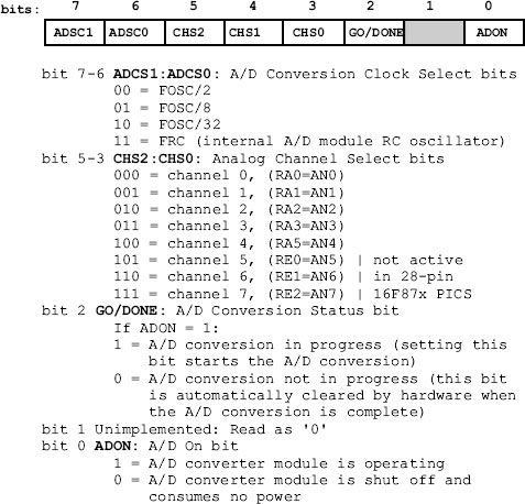
Figure 13-6 ADCON0 Register Bitmap.
The conversion time is the analog-to-digital clock period multiplied by the number of bits of resolution in the converter, plus the two to three additional clock periods for settling time, as specified in the data sheet of the specific device. The various sources for the analog-to-digital converter clock represent the main oscillator frequency divided by 2, 8, or 32. The third choice is the use of a dedicated internal RC clock that has a typical period of 2 to 6 μs. Because the conversion time is determined by the system clock, a faster clock results in a faster conversion time.
The A/D conversion clock must be selected to ensure a minimum Tad time of 1.6 μs. The formula for converting processor speed (in MHz) into Tad microseconds is as follows:
Where Tad is A/D conversion time, Tosc is the oscillator clock frequency in MHz, and Tdiv is the divisor determined by bits ADSC1 and ADSC0 of the ADCON0 register. For example, in a PIC running at 10 MHz, if we select the Tosc/8 option (divisor equal 8) the A/D conversion time per bit is calculated as follows:
In this case, the minimum recommended conversion speed of 1.6 us is achieved. However, in a PIC with an oscillator speed of 10 MHz, this option produces a conversion speed of 0.8 us, less than the recommended minimum. In this case we would have to select the divisor 32 option, giving a conversion speed of 3.2 μs.
Table 13.1
A/C Converter Tad at various Oscillator Speeds

In Table 13.1, converter speeds of less than 1.6 μs or higher than 10 μs are not recommended. Recall that the Tad speed of the converter is calculated per bit, so the total conversion time in a 10-bit device (such as the 16F87x) is approximately the Tad speed multiplied by 10 bits, plus three additional cycles; therefore, a device operating at a Tad speed of 1.6 μs requires 1.6 μs * 13, or 20.8 μs, for the entire conversion.
Bits CHS2 to CHS0 in the ADCON0 register (see Figure 13-6) determine which of the analog channels is selected. This is required, because there are several channels for analog input but only one A/2 converter circuitry. So the setting of this bit field determines which of six or eight possible channels is currently read by the A/C converter. An application can change the setting of these bits in order to read several analog inputs in succession.
Bit 2 of the ADCON0 register, labeled GO/DONE, is both a control and a status bit. Setting the GO/DONE bit starts A/D conversion. Once conversion has stared, the bit indicates if it is still in progress. Code can test the status of the GO/DONE bit in order to determine if conversion has concluded.
Bit 0 of the ADCON0 register turns the A/D module on and off. The initialization routine of an A/D - enabled application turns on this bit. Programs that do not use the A/D conversion module leave the bit off to conserve power.

Figure 13-7 Left- and Right-Justification of A/D Result.
The ADCON1 register also plays an important role in programming the A/D module. Bit 7 of the ADCON1 register is used to determine the bit justification of the digital result. This is possible because the 10-bit result is returned in two 8-bit registers; therefore, the six unused bits can be placed either on the left- or the right-hand side of the 16-bit result. If ADCON1 bit 7 is set then the result is right-justified, otherwise it is left-justified. Figure 13-7 shows the location of the significant bits.
One common use of right justification is to reduce the number of significant bits in the conversion result. For example, an application on the 16F877 that uses the A/D conversion module requires only 8-bit accuracy in the result. In this case, code can left-justify the conversion result, read the ADRESH register, and ignore the low-order bits in the ADRESL register. By ignoring the two low-order bits, the 10-bit accuracy of the A/D hardware is reduced to eight bits and the converter performs as an 8-bit accuracy unit.
The bit field labeled PCFG3 to PCFG0 in the ADCON1 register determines port configuration as analog or digital and the mapping of the positive and negative voltage reference pins. The number of possible combinations is limited by the four bits allocated to this field, so the programmer and circuit designer must select the option that is most suited to the application when the ideal one is not available. Table 13-2 (in the following page) shows the port configuration options.
For example, there is a circuit that calls for two analog inputs, wired to ports RA0 and RA1, with no reference voltages. In Table 13-2 we can find two options that select ports RA0 and RA1 and are analog inputs: these are the ones selected with PCFG bits 0100 and 0101. The first option also selects port RA3 as analog input, even though not required in this case. The second one also selects port RA3 as a positive voltage reference, also not required.
Either option works in this case; however, any pin configured for analog input produces incorrect results if used as a digital source. Therefore, a channel configured for analog input cannot be used for non-analog purposes. On the other hand, a channel configured for digital input should not be used for analog data because extra current is consumed by the hardware. Finally, channels to be used for analog-to-digital conversion must be configured for input in the corresponding TRIS register.
Table 13.2
A/D Converter Port Configuration Options

The A/D module can be made to operate in SLEEP mode. As mentioned previously, SLEEP mode operation requires that the A/D clock source be set to RC by setting both ADCS bits in the ADCON0 register. When the RC clock source is selected, the A/D module waits one instruction cycle before starting the conversion. During this period, the SLEEP instruction is executed, thus eliminating all digital switching noise from the conversion. The completion of the conversion is detected by testing the GO/DONE bit. If a different clock source is selected, then a SLEEP instruction causes the conversion - in - progress to be aborted and the A/D module to be turned off.
13.4.2 A/D Module Sample Circuit and Program
The circuit in Figure 13-8 is designed to demonstrate the use of the A/D converter module in PICs of the 16F87x family.

Figure 13-8 Demonstration Circuit for A/D Conversion Module.
Comparing Figure 13-8 with Figure 13-4, which uses the ADC0831 IC, we notice the economy of resources that results from selecting a PIC with an onboard A/D module. In the circuit of Figure 13-4, three microcontroller I/O ports must be used to connect the converter IC to the PIC. In the circuit of Figure 13-8, the potentiometer is connected directly to a single PIC port, saving two I/O lines. Considering the number of different PIC architectures that are equipped with onboard A/D converters, the circuit designer should explore this possibility before deciding on using a separate converter IC. At the same time, recall that two of the three input lines used by converter ICs can be shared. In a design with more than one converter IC, the use of input lines is not a 3 to1 ratio.
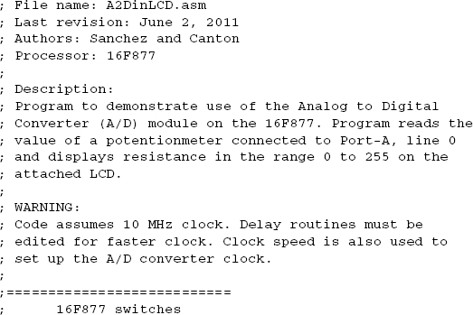
The circuit in Figure 13-8 consists of a 5K potentiometer wired to analog port RA0 of a 16F877 PIC. The LCD display is used to show three digits, in the range 0 to 255, that represent the relative position of the potentiometer’s disk. The program called A2DinLCD, in this book’s online software, uses the built-in A/D module.
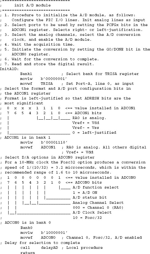
Programming the A/D module consists of the following steps:
1. Configure the PIC I/O lines to be used in the conversion. All analog lines are initialized as input in the corresponding TRIS registers.
2. Select the ports to be used in the conversion by setting the PCFGx bits in the ADCON1 register. Selects right- or left-justification.
3. Select the analog channels, select the A/D conversion clock, and enable the A/D module.
4. Wait the acquisition time.
5. Initiate the conversion by setting the GO/DONE bit in the ADCON0 register.
6. Wait for the conversion to complete.
7. Read and store the digital result.
The following procedure from the A2DinLCD program initialized the A/D module for the required processing:
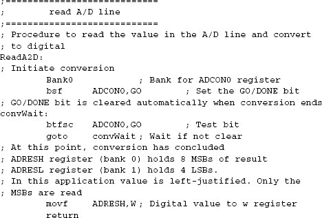
Once the module is initialized, the analog line is read by the following procedure:
The delay routine required in this case is coded as follows:

In the context of microcontrollers and embedded systems, real-time clocks (also called RTCs) are integrated circuits designed to keep track of time in conventional hours, that is, in years, days, hours, minutes, and seconds. Many real-time clock ICs are available with various characteristics, data formats, modes of operation, and interfaces. Most of the ones used in PIC circuits have a serial interface in order to save access ports. Most RTC chips provide a battery connection so that time can be kept when the system is turned off.
In the sections that follow, we discuss one popular RTC chip: the NJU6355, but this is by no means the only option for embedded systems.
13.5.1 NJU6355 Real-Time Clock
The NJU6355 series is a serial I/O real-time clock used in microcontroller-based embedded systems. The IC includes its own quartz crystal oscillator, counter, shift register, voltage regulator, and interface controller. The PIC interface requires four lines. Operating voltage is TTL level so it can be wired directly on the typical PIC circuit. The output data includes year, month, day-of-week, hour, minutes, and seconds. Figure 13-9 is the pin diagram for the NJU6355.
NJU6355 output is in packed BCD format, that is, each decimal digit is represented by a 4-bit binary number. The chip’s logic correctly calculates the number of days in each month as well as the leap years. All unused bits are reported as binary 0. Figure 13-10 is a bitmap of the formatted timer data.
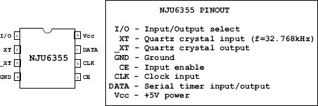
Figure 13-9 NJU6355 Pin Diagram.
Timer data is read when the I/O line is low and the CE line is high. Output from the 6355 is LSB first. A total of fifty-two significant bits are read in bottom-up order for data as shown in Figure 13-10. That is, the first bit received is the least-significant bit of the year, then the month, then the day, and so forth. All date items are eight bits, except the day of week, which is four bits. Nonsignificant bits in each field are reported as zero; this means that the value for the tenth month (October) is encoded as binary digits 00001010. Reporting unused digits as zero simplifies the conversion into BCD and ASCII.

Figure 13-10 NJU6355 Timer Data Format.
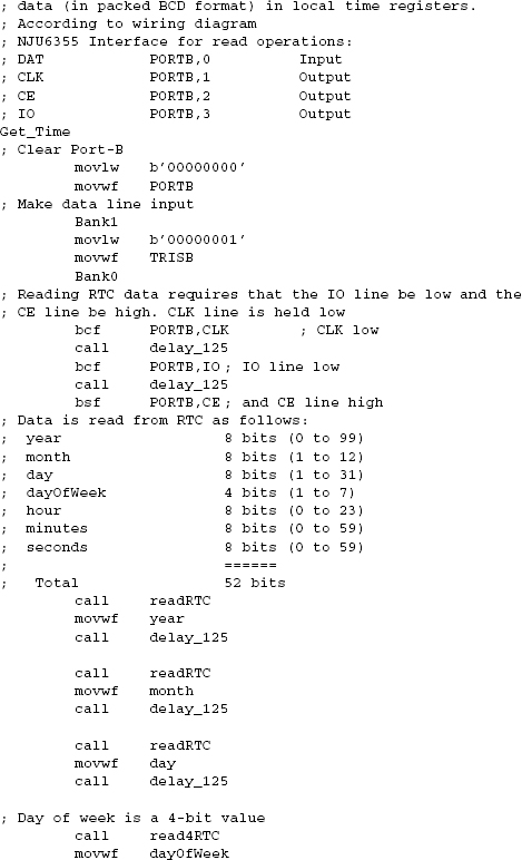
The NJU6355 does not report valid time data until after it has been initialized, even if there are power and clock signals into the chip. Initialization requires writing data into the 6355 registers. In order to write to the IC, code must set the I/O and the CE lines high. At this moment, all clock updates stop and the RTC goes into the write mode. Input data is latched in LSB first, starting with the year and concluding with the minutes. There is no provision for writing seconds into the RTC, so the total number of bits written is 44.
The 6355 contains a mechanism for detecting conditions that could compromise the clock’s operation, such as low power. In this case, the special value 0xee is written into each digit of the internal registers to inform processing routines that the timer has been compromised.
The NJU6355 requires the installation of an external crystal oscillator. The crystal must have a frequency of 32.768 KHz. The time-keeping accuracy of the RTC is determined by the quartz oscillator. The capacity of the oscillator must match that of the RTC and of the circuit. A standard crystal with a capacitance of 12.5 pF works well for applications that do not demand high clock accuracy. For more exacting applications, the 6355 can be programmed to check the clock frequency and determine its error. The chip’s frequency-checking mode is described in an NJU6355 Application Note available from New Japan Radio Co., Ltd.
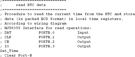
13.5.2 RTC Demonstration Circuit and Program
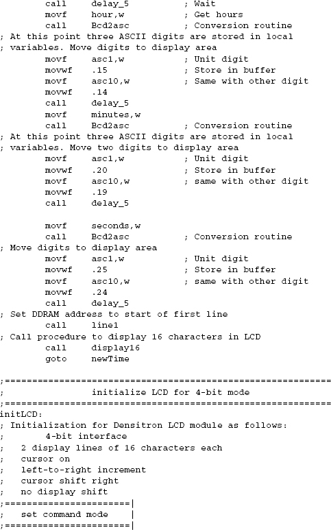
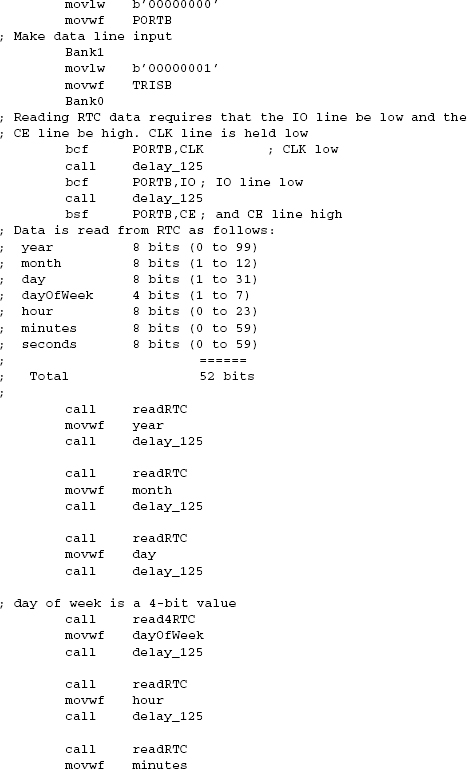
The circuit shown in Figure 13-11 is a simple application of the 6355 RTC. The circuit uses a NJU6355 in conjunction with a 16F86 PIC and an LCD. The demonstration program, named RTC2LCD, sets up RTC and reads clock data in an endless loop. The hours, minutes, and seconds are displayed at the top line of the LCD as follows:
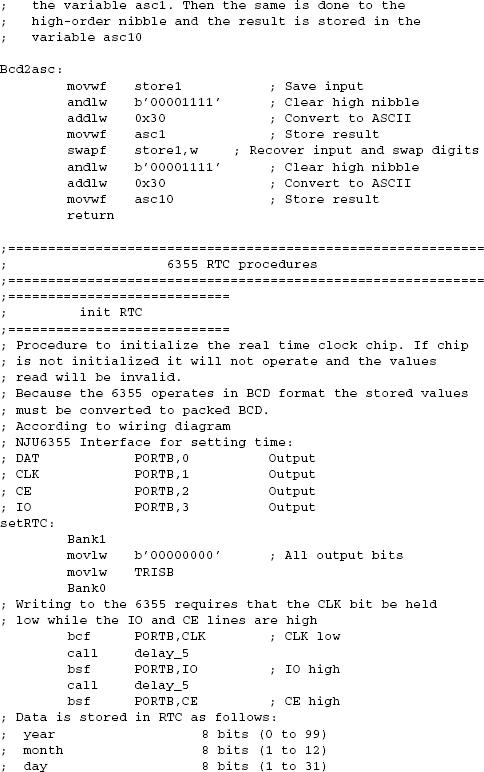
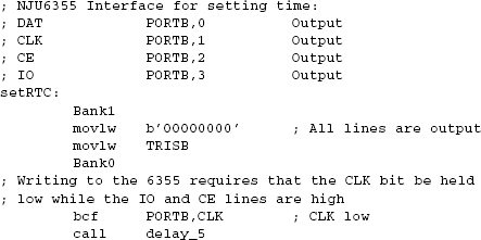
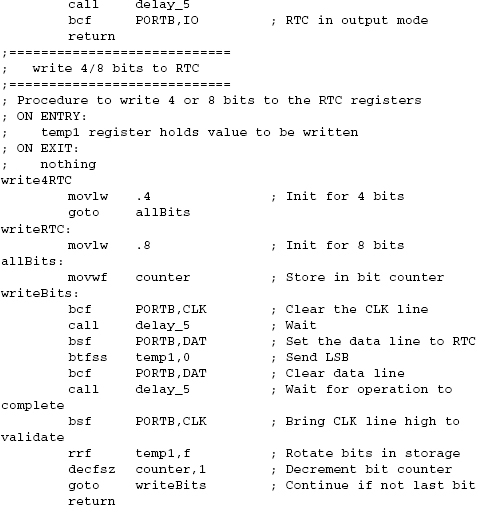
where xx represents the two BCD digits read from the clock and converted to ASCII decimal for display. The program initializes the 6355 to some arbitrary values contained in the corresponding #define statements. These values are copied into program variables by a local procedure and then used to initialize the RTC registers. Two procedures relate to RTC operation: one to initialize the clock hardware and the other one to read the current time. In addition, two auxiliary procedures are implemented: one to read clock data and one to write clock data. Because clock data can be in 8- or 4-bit formats, each procedure contains a separate entry point to handle the 4-bit option. The procedure to initialize and the one to write clock data are coded as follows:


Figure 13-11 Real-Time Clock Demonstration Circuit.

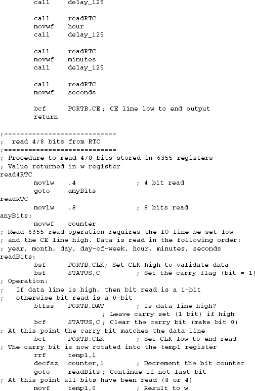
The following procedures are used by the RTC2LCD program to read the data in the RTC registers:
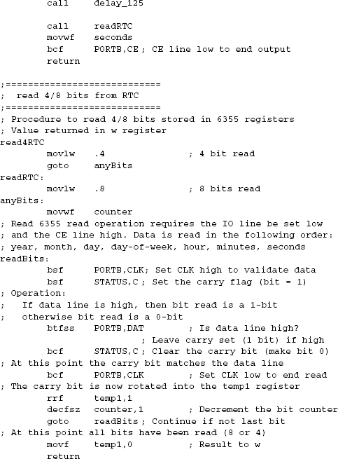
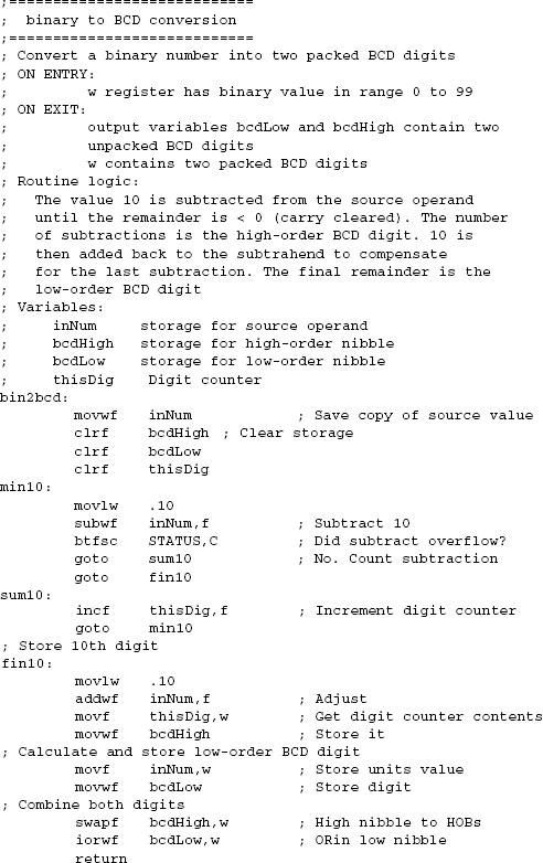
In addition to the RTC procedures to initialize the clock registers and to read clock data, the application requires auxiliary procedures to manipulate and display data in BCD format. BCD encodings are a way of representing decimal digits in binary form. Two common BCD formats are used: packed and unpacked. In the unpacked format, each byte encodes a single BCD value. In packed form, two BCD digits are encoded per byte. The 6355 uses the packed BCD format.
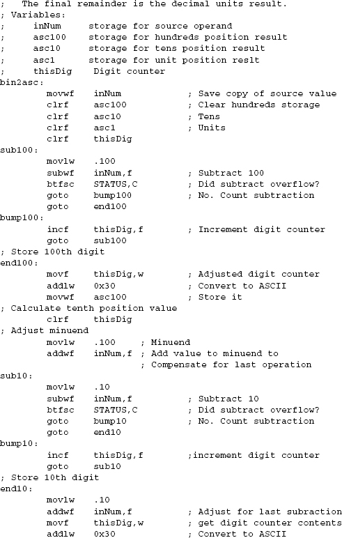
Because program data is usually in binary form, it is useful to have a routine to convert binary data into BCD form. A simple algorithm for converting binary to BCD is as follows:
1. The value 10 is subtracted from the source operand until the remainder is less than 0 (carry cleared). The number of subtractions is the high-order BCD digit.
2. The value 10 is then added back to the subtrahend to compensate for the last subtraction.
3. The final remainder is the low-order BCD digit.
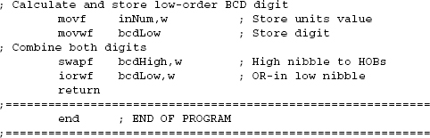
The binary to BCD conversion procedure is coded as follows:
Because the program requires displaying values encoded in BCD format, a routine is necessary to convert two packed BCD digits into two ASCII decimal digits. The conversion logic is quite simple, as the BCD digit is converted to ASCII by adding 0x30 to its value. All that is necessary is to shift bits in the packed BCD operand so as to isolate each digit and then add 0x30 to each one. The routine’s code is as follows:

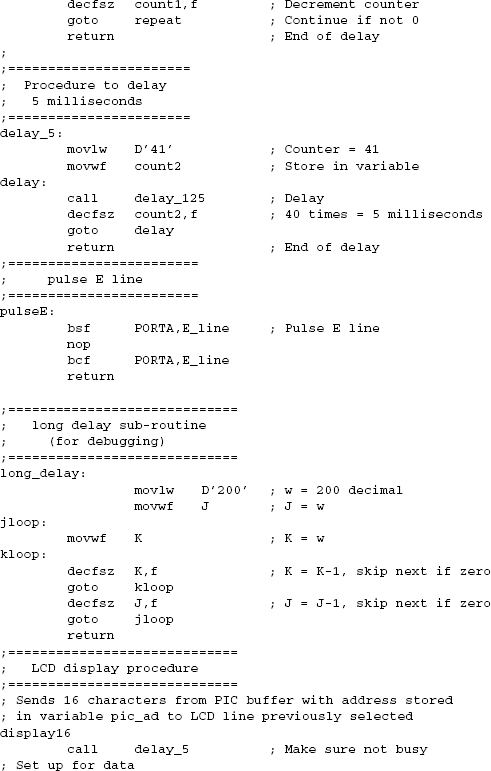
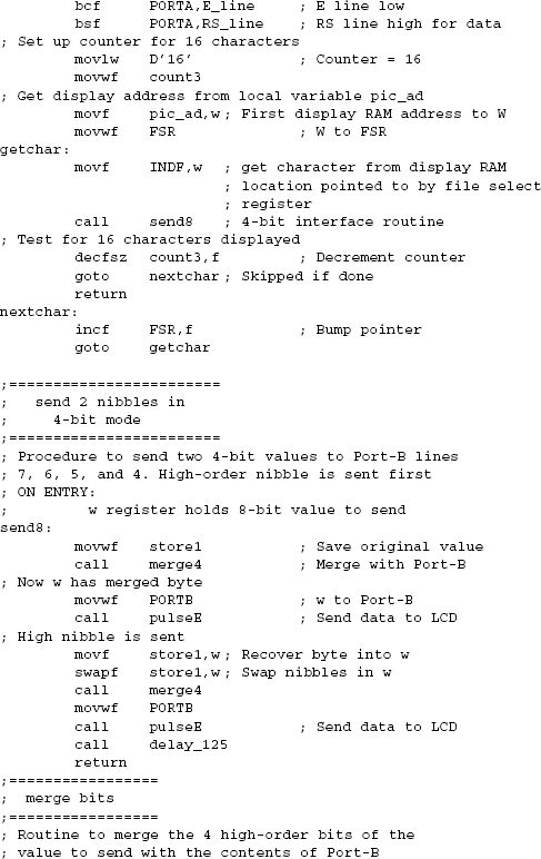
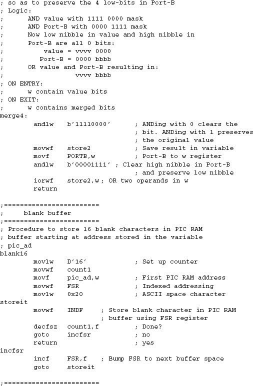
The following subsections contain the sample programs discussed in this chapter.