
12
Analog ESD and Latchup Design Rule Checking and Verification
In this chapter, the focus is on electronic design automation (EDA) associated with electrical overstress (EOS) design. This continues to be a growing issue, as new concepts and techniques are developed. In this chapter, electrostatic discharge (ESD) concepts will also be highlighted due to the similarity of concepts for both EOS and ESD EDA. Latchup electronic design automation (EDA) techniques relevant to EOS issues will also be shown.
12.1 Electronic Design Automation
EDA is a software tool specifically for the design of electronic systems such as single components, integrated circuits, and printed circuit boards (PCBs). EDA tools can be applied to ESD [1–28], EOS [25], latchup [11, 29–54], and other electromagnetic compatibility (EMC) issues. In this chapter, the focus will be on how EDA and computer-aided design (CAD) can be utilized to provide more robust electronic systems addressing whole-chip analysis and cross-domain issues in mixed-signal (MS) system-on-chip (SOC) applications [23, 55–69]. Figure 12.1 is an example of the checking and verification needs today in an EOS environment.

Figure 12.1 Checking and verification.
12.2 Electrical Overstress (EOS) and ESD Design Rule Checking
EOS and ESD design rules will be discussed in this section [1–3]. As new problems and issues arise in integrated circuits and SOC applications, these rules continue to be added. In this chapter, we will touch on a few examples of how to apply these to EOS, ESD, and latchup.
12.2.1 ESD Design Rule Checking
In semiconductor chip design, ESD design rule checking (DRC) is presently part of the ESD design discipline. In the 1980s, no ESD design rules existed in the majority of corporations. In some of the first corporations, in the 1990s, ESD design rules were first integrated into the methodology of DRC where physical dimensions could be verified.
In ESD design rule development, the rules are defined to improve and to satisfy the ESD specifications for the qualification and release of the semiconductor components (Figure 12.2). The ESD specifications of interest for the qualification and release of components from manufacturing are the human body model (HBM) and charged device model (CDM).

Figure 12.2 Electrostatic discharge (ESD) design rule check.
The ESD design rules are as follows [1–3]:
- Existence rule of an ESD network on all bond pads
- Wire width rule for interconnects between bond pads and ESD networks
- Number of contacts for interconnects between bond pads and ESD networks
- Number of vias for interconnects between bond pads and ESD networks
- Wire width rule for interconnects between ESD networks and power rails
- Number of contacts for interconnects between ESD networks and power rails
- Number of vias for interconnects between ESD networks and power rails
- ESD network for HBM specification compliance
- ESD network series resistor rule for receiver networks
- ESD network for CDM specification compliance
- ESD HBM network device width
- ESD CDM network device width
- ESD power clamp between power and ground (e.g., VDD and VSS)
- ESD rail-to-rail networks between ground rails (e.g., VSS to VSS)
- ESD network-to-ESD power clamp placement rule
- Cross-domain ESD network
- Cross-domain signal line ESD network between domains (e.g., analog-to-digital signal line)
- Differential pair pin-to-pin ESD network
12.2.2 Electrostatic Discharge Layout-versus-Schematic Verification
In ESD checking and verification, layout versus schematic (LVS) is used to insure proper implementation [1–28]. The LVS verification is a class of EDA verification software. The LVS verification is used to insure that there is proper correspondence between a design layout and a circuit schematic within an integrated circuit chip. LVS checking software recognizes the layout of a particular design and evaluates the drawn shapes of the layout; these drawn shapes represent the electrical components of the circuit and connectivity. LVS verification involves three steps: extraction, reduction, and comparison.
For ESD protection, LVS can verify the correct physical layout that is utilized for a given ESD network; this can be achieved through netlist verification. In some semiconductor chip implementation, the incorrect layout is used for the ESD network; this can lead to failure of the desired ESD specification objectives.
LVS can also be used to insure the ESD network is connected to a given signal or power pin. In many chip designs, there are cases where the design team does not place an ESD network on a given signal pin. Additionally, receivers may require two networks—one for HBM and machine model (MM) objectives and a second network for CDM protection. For sensitive receiver networks, this can lead to failing all specification, or passing one, but not the other.
It is also important to insure the correct ESD network is applied to the correct circuit. In many complex applications, mismatch between the circuit and the corresponding ESD network can occur. Using the incorrect ESD network for a corresponding signal pin can lead to functional test failure, or ESD failure.
12.2.3 ESD Electrical Rule Check (ERC)
In semiconductor chip design, ESD electrical rule check (ERC) is presently part of the ESD design discipline to insure proper operation of the ESD networks to shunt current to power or ground and to establish a low impedance alternate current path for discharge of the ESD current. Providing good ESD protection can lead to improvements to EOS by discharging EOS current through the semiconductor chip.
In ESD ERC development, the rules are focused on the resistance. By providing high series resistance, ESD current-limiting protection solutions can prevent failure of circuitry on the signal path. By providing a low resistance in the ESD network, wiring, and power rails, ESD current can be shunted through an alternate current path for discharge of the ESD current. The ESD specifications of interest for the qualification and release of components from manufacturing are HBM and CDM.
The ESD design rules are as follows:
- Wire resistance rule for interconnects between bond pads and ESD networks
- Contact resistance for interconnects between bond pads and ESD networks
- Via resistance for interconnects between bond pads and ESD networks
- Power rail wire resistance rule for interconnects between ESD networks and power rails
- Power rail contact resistance for interconnects between ESD networks and power rails
- Power rail via resistance for interconnects between ESD networks and power rails
- ESD network series resistor resistance rule for receiver networks
- ESD HBM network device resistance
- ESD CDM network device resistance
- Cross-domain signal line ESD network series resistance (e.g., analog-to-digital signal line)
12.3 Electrical Overstress (EOS) Electronic Design Automation
EDA tools are very important for evaluation of EOS robustness of systems [1]. For EOS, one must evaluate the EOS protection devices, the PCB, and the ESD protection scheme. In the following sections, EOS protection networks and PCB design rules and checks are discussed.
12.3.1 Electrical Overstress (EOS) Design Rule Checking
EOS robustness can be achieved through DRC of all elements in the system [1]. This includes the EOS protection elements, the PCB, and the components themselves.
EOS DRC can be established in the EOS elements themselves. Examples of DRC rules for EOS protection devices can include (Figure 12.3):
- EOS protection device width
- EOS protection device ground rule dimension checks
- EOS protection device interconnect wiring
- EOS protection device internal bond pads
- EOS protection device wire bonds
- EOS protection device parasitic evaluation

Figure 12.3 Electrical overstress (EOS) design rule check.
EOS DRC can also be applied to the PCB design rules; this will be highlighted in a later section. EOS protection rules can be also developed for the onboard components to check to see if the components can survive the voltage and current condition of EOS events.
12.3.2 Electrical Overstress (EOS) Layout-versus-Schematic (LVS) Verification
In EOS, checking and verification is important to avoid functionality concerns, field failure, or integration errors. EOS LVS checking and verification can be used to insure proper implementation [1].
The LVS verification can insure that there is proper correspondence between a design layout and a circuit schematic within an integrated circuit chip. For EOS, LVS checking software can be used for proper integration of PCBs, EOS protection devices, and on-chip ESD protection. What is unique to EOS events, the cards, PCB, and components require verification.
EOS LVS checking and verification can address the following design errors:
- Electrical shorts
- Electrical opens
- Electrical parameter mismatch
- Mismatch of EOS protection networks and ESD protection networks
In EOS verification, it is important to check and verify that the correct EOS protection device is on the correct signal pin (Figure 12.3) as well as device directionality (Figure 12.4). EOS protection circuits can be diodes, Schottky diodes, Zener diodes, varistors, gas discharge tubes, and a plethora of other protection schemes [1]. First, it is important to verify that the EOS protection device is a valid supported device. Second, it is important to verify that the one chosen satisfies the current-limiting resistance, or voltage trigger level. Additionally, it is important to verify that the element is suitable for the application.

Figure 12.4 Checking and verification of correct EOS protection device.
Another key issue is the EOS protection device directionality. The EOS element directionality must also be suitable for the signal application. As part of the LVS checking, it is important that the correct nodes of the EOS element are the desired orientation and that electrodes are not reversed (Figure 12.5).

Figure 12.5 Checking and verification of correct EOS protection device directionality.
12.3.3 Electrical Overstress (EOS) Electrical Rule Check (ERC)
EOS ERC can provide a means of checking and verification of conformance to EOS product specification [1]. An EDA methodology can reduce the risk of field failures and field returns. For EOS events, it is necessary to evaluate the semiconductor chip, package, and PCB for checking and verification.
An EOS ERC methodology can include the following items:
- PCB trace resistance
- PCB trace maximum allowed current magnitude
- PCB components series resistance
- EOS current-limiting protection device resistance
- EOS voltage clamp protection device shunt resistance
- Component pin resistance
- Component bond wire maximum allowed current magnitude
- Component bond wire resistance and inductance
- On-chip ESD protection circuit series resistance
- On-chip ESD protection circuit shunt resistance
- On-chip ESD protection circuit-to-bond pad resistance and current limit
- On-chip ESD protection circuit-to-power rail interconnect resistance and current limit
- On-chip power rail-to-ESD power clamp interconnect resistance and current limit
- On-chip power rail VDD interconnect resistance and current limit
- On-chip power rail VSS interconnect resistance and current limit
For 2.5-D and 3-D systems, additional evaluations should be verified that include silicon interposers and through-silicon vias (TSV):
- Silicon interposer trace resistance and allowed current-carrying capability
- TSV resistance
12.3.4 Electrical Overstress Programmable Electrical Rule Check
EOS programmable ERC (PERCTM) can provide a means of checking and verification of conformance to EOS product specification [25]. An EDA methodology can reduce the risk of field failures and field returns.
The desired lifetime of the circuit and the type of environment(s) in which the circuit will operate are important for reliability assessment and evaluation of EOS. EOS events are a function of the external temperature, electrical, magnetic, and mechanical stresses to which the circuit will be susceptible. Calibre® PERC can be used to prevent electrical circuit failure due to EOS and improve overall circuit reliability [25].
Using topological verification methods, Calibre PERC can be used to insure that these ESD structures and devices have been implemented properly. Additionally, the interconnect wire width can be verified to insure no ESD or EOS failures. For EOS events, the tool can also provide voltage propagation into the circuit to evaluate overvoltage stress from residual currents in a design [25].
12.4 Printed Circuit Board (PCB) Design Rule Checking and Verification
In the design of the PCB, EDA design rules can be established associated with EOS, electromagnetic interference (EMI), and the EMC characteristics. EOS DRC can be easily established for the following [1]:
- Number of design levels
- Power plane design
- Ground plane design
- Signal plane design
- Trace line impedance
- Copper routing thickness
- Trace width
- Component placement
- Signal trace routing
Electronic design rule checks can be developed to address physical placement. Some design checks for placement and component selection are listed below [1]:
- Connector edge placement check
- Connector corner placement check
- Common connector
- Connector to onboard I/O components spacing check
- Connector and I/O to onboard non-I/O components spacing check
- Clock and clock oscillator placement check
Trace routing and power/ground plane decisions are key to avoid EMI, EMC, and EOS concerns.
These can be checked and verified using EDA tools:
- Power trace EOS width
- Ground trace EOS width
- Signal trace EOS width
- Critical signal trace placement
- Non-I/O trace placement
- Non-I/O trace placement and I/O components
- Signal trace and power plane separation
- Signal trace and ground plane separation
- I/O to connector trace length
- Trace length
- Trace to board edge
- Differential signal trace pairs
More sophisticated design tools can evaluate many design variables in PCB design. EDA tools can address the following (Figure 12.6):
- Identify EMI sources and victims
- Identify critical paths
- Identify potential antennae issues
- Identify coupling mechanisms

Figure 12.6 PCB design checking steps.
12.5 Electrical Overstress and Latchup Design Rule Checking (DRC)
EOS and latchup DRC are important to avoid electrical failure of components and PCBs. Latchup events can lead to melting of the component and its packaging. Hence, in providing an EOS robust solution, it is important to understand the limitation associated with CMOS latchup.
12.5.1 Latchup Design Rule Checking
EOS can lead to latchup in semiconductor components and systems. Latchup tolerance can be minimized through semiconductor chip process technology, design layout, circuit design, and system design. EDA can be used to check and verify latchup robustness of a component on a semiconductor chip level [11, 29–47].
Latchup DRC is important to avoid latchup concerns in semiconductor components. In the 1980s, semiconductor corporations and foundries had few means of using EDA tools to check and verify for latchup. The first latchup sections were being placed in technology design manuals in the mid-1980s [32, 33].
Today, latchup DRC are included within the design checking and verification. Latchup can occur in semiconductor devices in the following categories:
- Latchup between devices within a common circuit
- Latchup between devices between different circuits
- I/O circuit to I/O circuit latchup
- I/O circuit to ESD circuit latchup
- I/O circuit to core circuit latchup
- Domain-to-domain latchup
To address these issues, the solutions from a layout and design perspective can be achieved through physical spacing, separation of domains, and placement of guard rings to avoid formation of a parasitic pnpn that can lead to latchup. Latchup DRC categories include the following (Figure 12.7) [11, 29–54]:
- Placement of connections to power rails relative to devices
- Device-to-device placement
- Circuit-to-circuit placement
- Existence of guard ring structures and spacing around devices
- Existence of guard ring structures and spacing between devices
- Existence of guard ring structures and spacing between circuits
- Existence of guard ring structures and spacing between separate power domains
- Existence of guard ring structures and spacing between semiconductor chip cores

Figure 12.7 Latchup DRC.
In CMOS latchup, the physical dimensions associated with the parasitic pnpn network are checked and verified (Figure 12.8). CMOS latchup is a function of four fundamental variables. In a DRC, these are checked independently. In addition, there are guard ring rules. Fundamental DRC includes the following [11, 29–54]:
- Minimum p+ to n-well space: The physical space between the p+ diffusion and the n-well edge is set to some minimum value based on the desired p+/n+ minimum rule.
- Minimum n+ to n-well space: The physical space between the n+ diffusion and the n-well edge is set to some minimum value based on the desired p+/n+ minimum rule.
- Maximum n-well resistance requirement: The maximum n-well resistance is established based on the maximum allowed well shunt resistance. This is typically represented as a physical distance between the n-well contact and the p-channel MOSFET or any p-doped element in an n-well region.
- Maximum p-substrate resistance requirement: The maximum substrate resistance is established based on the maximum allowed substrate shunt resistance. This is typically represented as a physical distance between the p-well contact and the n-channel MOSFET or any n-doped element in a p-well region.
- Guard ring-type rule: Design rules require guard rings for all elements electrically connected to an external node. The type of guard rings is a function of whether an element is p-doped or n-doped, and the technology requirements. Typically, n-well guard rings are placed around n-diffusions. In many technologies, double guard rings are used (e.g., a p+ substrate ring as well as an n-well guard ring). In BiCMOS technologies, deep trench (DT) can be utilized to improve both CMOS latchup robustness and noise injection.
- Minimum guard ring space rule: Typically, the guard rings are spaced relative to the physical diffusion to allow electrical biasing without interaction. In addition, the spacing is optimized as to not be too close to elements to establish interaction but at the same time at a distance too far where they do not collect minority carrier injection.
- Minimum guard ring width rule: Guard ring width influences the guard ring efficiency of a guard ring structure. Hence, many technology guidelines will define the width or choose a minimum width for guard ring designs.
- Maximum guard ring resistance rule: In many technologies, either the guard ring design is defined or a maximum guard ring resistance rule is established.
- Butted contact rules: In many technologies, butted contacts are desired to minimize the resistance between a contact and the device, recommending that butted contacts should be utilized to minimize latchup concerns. In other technologies, this issue is avoided.

Figure 12.8 Ground rules for internal latchup.
In a CMOS technology, there are many parasitic transistors inherent in the devices. In the extraction process of parasitic transistors in a physical design, there are a large number of parasitic transistors. In a multifinger MOSFET, each independent finger of the MOSFET can appear as a multifinger emitter or multifinger collector. Given there are p emitters and q collectors, there is a potential of pq-independent bipolar transistors that can be extracted. As a result of this complexity, there must be a simplification methodology to reduce the problem to a smaller set; this is done through reduction rules. T. Li highlighted three practical reduction rule cases to simplify the extraction process. In these rules, they evaluate (i) the electrical state and (ii) the bipolar current gain [12, 13].
Figure 12.9 is a drawing of the first reduction rule. A first reduction rule is the case of the “shared emitter rule.” In a shared emitter rule, each independent collector has an independent voltage state and an independent bipolar current gain. The bipolar current gain can be obtained by determining the collector area and the geometric spacing relative to the emitter of interest. In this reduction process, the collectors that are farthest away and the lowest voltages are removed [12, 13].

Figure 12.9 Latchup parasitic bipolar DRC shared emitter rule.
Figure 12.10 is a representation of the second reduction rule. A second reduction rule is the case of the “shared collector rule.” In a shared collector rule, each independent emitter has an independent voltage state and an independent bipolar current gain. The bipolar current gain again can be obtained by determining the emitter area and the geometric spacing relative to the collector of interest. In this reduction process, the emitters that are farthest away and the lowest voltages are removed [13].
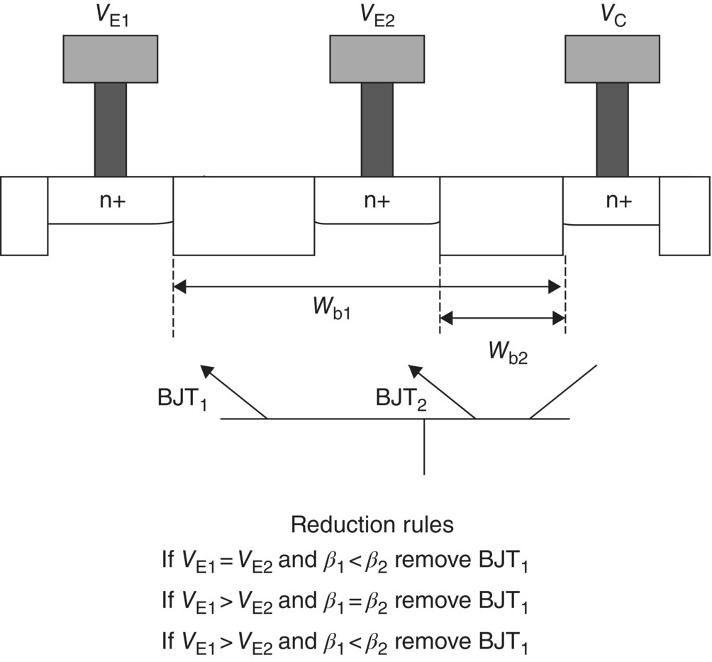
Figure 12.10 Latchup parasitic DRC shared collector rule.
A third rule is a “minimum bipolar current gain rule.” Given a bipolar current gain was less than a given value, the bipolar parasitic transistor is not evaluated. For example, given a bipolar current gain is less than unity, it can be removed [13].
It is clear from this framework and methodology that additional rules can be defined for pnpn elements. Hence, a CMOS CAD methodology can utilize reduction rules as a means of sorting out the important parasitic bipolar transistors for CMOS latchup.
When a secondary current source external to the circuit exists, this is referred to as “external latchup.” In the case of this secondary source, CMOS latchup can occur [30, 31]. The secondary source can be injection current from other circuits or other power domains.
When the secondary source is adjacent to a given sensitive circuit, the latchup robustness of the circuit can be improved by decreasing the substrate and well contact spacings to a CMOS transistor.
12.5.2 Latchup Electrical Rule Check (ERC)
In the designing of semiconductor components, latchup rules are defined for layout, circuit, and electrical characteristics. Latchup involves design layout, circuit interaction, and product current and voltage conditions [30, 31].
Latchup ERC is introduced to provide prevention of latchup due to excessive resistance [30, 31]. ERC can be introduced for a few key areas:
- N-well contact to p-channel MOSFET resistance
- P-well or p-substrate contact to n-channel MOSFET resistance
- Guard ring resistance
12.5.2.1 N-Well Contact to P-Channel MOSFET Resistance
An n-well resistor exists between the power supply (VDD) and the p-channel MOSFET channel region. The n-well resistance is a function of the spacing between the physical contact to the n-well region and the p-channel MOSFET, the width of the contact region, the width of the MOSFET, and the n-well sheet resistance. For prevention of CMOS latchup, it is best to lower this value to prevent forward biasing of the p-diffusion to n-well junction.
12.5.2.2 P-Well or P-Substrate Contact to N-Channel MOSFET Resistance
A p-well resistor exists between the power supply (VSS) and the n-channel MOSFET channel region. The p-well resistance is a function of the spacing between the physical contact to the p-well region and the n-channel MOSFET, the width of the contact region, the width of the MOSFET, and the p-well sheet resistance. For prevention of CMOS latchup, it is best to lower this value to prevent forward biasing of the n-diffusion to p-well junction.
12.5.2.3 Guard Ring Resistance
Guard rings are used to collect the minority carrier injection into the well and substrate regions of a semiconductor device. Guard rings constructed from metallurgical junctions allow collection of the minority carriers to prevent interaction with other devices, circuits, domains, or cores. For the guard rings to be effective, the electrical resistance between the point of collection and the power rails will be required to be low enough for efficient collection and prevention of forward biasing of the guard ring-to-substrate or guard ring-to-well metallurgical junction.
In the integration of guard rings into a semiconductor chip design, CAD methods are being used for latchup. Guard rings are placed around injection sources that can trigger latchup. Injection sources can be n+ diffusions, n-type resistors, and n-wells (e.g., in a p-type substrate wafers). One of the primary design issues with guard rings is the effectiveness to collect the minority carrier injection. The guard ring effectiveness is dependent on the guard ring type, the guard ring depth, guard ring physical width, and relative spacing from the injection source. Guard ring resistance is also a key criterion. The reasons this is a growing issue are the CMOS and BiCMOS dimensional scaling and increase in the peripheral I/O density (e.g., I/O book width scaling). With the technology dimensional scaling, the physical dimensions of the p+, n+, and n-well have been reduced. With the scaling of the minimum n-well widths, the width of n-well guard ring has been scaled. As a result, the resistance along the length has increased. With the increase in circuit density, the I/O circuit density has increased. ASIC environments have focused on reducing the width of the I/O peripheral book to allow more I/O circuits on the periphery of a semiconductor chip. In this process, the peripheral I/O length has been increased to compensate the reduction of the peripheral I/O book width.
With the placement of an n-type guard ring in the p-type substrate, a metallurgical junction is formed which can collect the minority carrier electrons injected into the substrate. As an example, an n-type guard ring is biased to the power supply voltage, collecting the injection current.
At low injection currents, the electrons are collected by the reverse-biased metallurgical junction formed between the substrate and the n-type guard ring. But, at very high injection currents, the series resistance between the power supply voltage and the guard ring is a key latchup design factor.
The injection source serves as an “emitter,” the substrate serves as a “base” region, and the guard ring serves as a “collector.” When the emitter–base junction is forward active, the electrons are injected into the substrate region. When the collector is biased positive at the power supply voltage, the collector-to-emitter voltage is positive. In this state, the parasitic transistor formed between the injection source and the guard ring is forward active. When the resistance of the guard ring increases, a voltage drop occurs in the guard ring. The voltage drop is equal to the product of the guard ring resistance and the injection current:
where Iinj is the injection current and RGR is the guard ring resistance between the point of injection and the power supply voltage. At the location of the injection, the voltage at the guard ring is equal to
As the voltage drop increases due to the injection current, the guard ring voltage at the point of injection will decrease. When the effectiveness of the guard ring to collect the current is minimized as a result of the debiasing, the minority carrier electron current will flow to alternative structures (e.g., outside of the guard ring). Design parameters that influence the resistance are the following:
- Guard ring sheet resistance (e.g., n-well sheet resistance or plurality of implants in the guard ring)
- Guard ring width
- Guard ring contact density
- Guard ring contact resistance
- Guard ring silicide resistance
- Metal bus resistance
- Distance between the injection location and the power supply voltage source
Historically, guard ring resistance was not a critical issue due to the technology, the ground rule dimensions, and the I/O density. From the 1980s to 2000, the guard rings used were typically n-well regions. In this time frame, the ground rules for both diffused and retrograde wells prevented narrow width n-well regions. As a result, the ground rules prevented scaling of the guard ring widths below some minimum dimension (e.g., typically, wells could not be scaled below 3–7 µm). With the utilization of the n-diffusion, silicides (e.g., titanium silicide and cobalt silicide), and large contact dimensions, the resistance was very low. Additionally, due to wide “wiring tracks” and peripheral I/O design, the power bus width was wide (e.g., 10–30 µm). In addition, the I/O density was low.
In this millennium, the vertical semiconductor process profile was scaled, leading to higher well sheet resistance. In addition, vertical scaling allowed for a decreased minimum well width requirement allowing a narrower guard ring structure in I/O design. In each technology generation, the number of I/O increases leading to high aspect ratio I/O books that are long and narrow. In this case, the guard ring width is reduced, and the length between injection sources and the power supply voltage are increased. In addition, with the metal scaling, the wire widths are reduced to allow a higher density of wire tracks. With all the scaling issues for both the semiconductor process and the semiconductor chip layout design, the resistance issue is more critical.
A CMOS latchup CAD system can be developed that addresses the guard ring resistance [30]. The CMOS latchup CAD evaluation must address a maximum resistance requirement for the guard ring resistance (Figure 12.11). The guard ring resistance can be evaluated as follows:
- Identify injection source.
- Identify the location near the guard ring structure.
- Calculate the total resistance to the power supply VDD.
- Evaluate the maximum resistance allowed for the guard ring for the given conditions.

Figure 12.11 Guard ring resistance ground rule with injection source.
A key latchup design practice is as follows:
- Establish a guard ring structure under the condition of maximum resistance criteria.
- Establish a resistance criteria associated with a resistance calculation from the location of injection sources and its intersection at the guard ring to the power supply voltage location which “sinks” the latchup current. The effective resistance of all structures is used in the resistance calculation (e.g., sheet resistance, silicides, contact, and metal bussing).
12.6 Whole-Chip Checking and Verification Methods
Whole-chip ESD checking and verification methods have been a significant challenge in the semiconductor industry. Whole-chip ESD checking and verification has been the “holy grail” of semiconductor chip design. Today, there is still no standard checking and verification tool that is used in the foundry business [23, 55–69].
Due to Moore’s law technology scaling, the number of circuits continues to increase each technology generation. With the increase in the number of circuits on a chip, the number of peripheral I/O continues to increase according to Rent’s rule.
The complexity of semiconductor chips continues to increase with mixed-voltage interface (MVI), MS, SOC, and 3-D multichip environments. Technologies support digital, analog, power, and RF domains in a common chip or multichip system. With the increased complexity, multiple power and grounds exist for each domain.
The whole-chip verification methods focused on HBM and CDM ESD events. HBM methods address ESD critical discharge paths between the bond pad and power rails. These HBM-based checking and verification methods evaluate the voltage drop along the discharge path, between two pads. CDM checking and verification methods evaluate voltage clamping on each pad.
With the increase in chip size, and the number of bond pads, the run time increases. Checking and verification systems require methods to reduce the netlist and run time [64–69]. A methodology to reduce the run time was the representation of each domain as a “macro model” for each power domain was developed. A CDM event was performed on the network to focus on the cross-domain signals. A second methodology simulated CDM events on a reduced netlist and applied a random walk [61]. Another method reduces the netlist to only include elements in the ESD current path and initiate a SPICE circuit pre- and postprocess [64]. Other methodologies check all circuit elements electrically connected to bond pads. In these methods, cross-domain signal lines and interconnections of elements in these domains are not all addressed.
12.7 Cross-Domain Signal Line Checking and Verification
With the increase in complexity, the number of cross-domain signal lines increases. Cross-domain signal lines are a source of ESD failures. Hence, methods are required for identifying these cross-domain signal lines where ESD failures exist internal to the semiconductor chip. New methodologies focus on these cross-domain signal lines and the internal ESD failures.
12.7.1 Cross-Domain Signal Line Checking and Verification Flow System
With the increase in complexity, the number of cross-domain signal lines increases. Cross-domain signal lines are a source of ESD failures. A full-chip ESD verification methodology that focuses on internal interfaces between power and ground is discussed by Z. Lu and D.A. Bell [62].
In this methodology, the focus uses the device netlist topology to check all domains crossing interfaces, as well as the ESD networks in the domains. The checking and verification method checks the design hierarchically. This method utilizes a “bottom-up” approach where the checking is done cell by cell; this is achieved using a novel concept of a topology-aware net type.
Figure 12.12 shows the verification flow diagram. The verification uses a SPICE netlist which is either a circuit schematic or layout based. In the chip layout netlist, this methodology must identify ESD protection networks. In this method, an ESD rule deck supports the ESD verification engine. The ESD rule deck identifies the power and ground rails, as well as ESD-related information. The hierarchical algorithm has two fundamental steps: an initialization step and rule checking step. The initialization step collects the ESD-related topology information. In the second step, the rule checking step, the algorithm checks the ESD rules, cell by cell.

Figure 12.12 Verification flow.
In this method, there is a topology-aware net type and a topology-aware path type. The topology-aware net type recognizes that a device is contained in a cell; this allows for finding elements associated with ESD protection. Secondly, a topology-aware path type identifies the electrical current paths. These net types and net path types are propagated across the design. Figure 12.13 shows an example where the cross-domain signal has both a net type and path type associated with the signal line in both the domains.

Figure 12.13 Interdomain signal line verification and checking.
This methodology introduces a hierarchical methodology that does not require netlist reduction. With the utilization of hierarchical method, each cell is evaluated independently.
12.7.2 Cross-Domain Analog Signal Line Checking and Verification Flow System
In analog design, with the complexity of the ESD library, additional requirements are needed to provide ESD checking and verification. Figure 12.14 shows an example of a different analog overall verification flow [63]. The key features of this analog ESD checker are as follows:
- Identify the ESD cell
- Verify ESD product requirement fulfillment (e.g., capability)
- Verify ESD that does not impact functionality (e.g., transparency)
- Verify existence of ESD cell (e.g., availability)

Figure 12.14 Analog design overall verification and checking.
An analog design verification system must have the following characteristics:
- Support a large component portfolio
- Support a diverse component type (e.g., CMOS, LDMOS, BCD)
- Support a large ESD library
- Check complex circuits
- Validation of layout check
The validation of the ESD cell is key to this methodology. The methodology addresses validating capability, transparency, and availability. The tool has the ability to reduce the size of the network analyzed by topology matching and introduces model simplification by the use of a “black box” path representation of ESD cells and technology components.
In this methodology, the cross-domain issues can be evaluated. This is achieved by extraction of the ESD cells and resistances. The tool identifies “at-risk constructions” where unintentional cross-domain connections exist that could lead to ESD failures. The methodology has the ability to “jump” over predefined series components to identify the “at-risk” topology across two domains.
12.7.3 Cross-Domain Checking and Verification: Resistance Extraction Methodology
Cross-domain checking and verification are important in MS semiconductor applications and can be integrated into whole-chip ESD simulation [64–69]. In this whole-chip methodology, the ESD paths are evaluated including power and ground connections. To address the voltage conditions in cross-domains, it is important to extract the power rail, ground rail, ESD power clamp, and signal line resistances. Figure 12.15 is a transformation of the cross-domain environment into an equivalent circuit of resistances and capacitances, forming a general cross-domain ESD network model. In Figure 12.15, two inverters are electrically connected by a signal line. The ESD event occurs between the two bond pads represented. The ESD power clamps within the separate domains are reduced to extracted equivalent circuits represented as resistors and capacitors. The ground and power busses are represented as series resistors. In Figure 12.16, a simplified full resistance cross-domain ESD network model is represented.

Figure 12.15 Cross-domain analysis including both equivalent resistance and capacitance.

Figure 12.16 Cross-domain resistance analysis.
Figure 12.17 shows a flow chart for the cross-domain ESD simulation. The methodology includes the following steps:
- Extract ESD power clamp from I/O GDS without using SPICE/CDL netlists.
- Generate a figure-like metal and vias on the ESD power clamp.
- Set the resistance parameter based on the on-resistance of the ESD power clamp.
- Determine voltage drop using commercial voltage drop tool using the transformed I/O layout, LEF, and DEF.
- Generate a voltage drop map.
- Use current density map to check wire widths and power clamp size.
- Extract receiver and driver cell location information.
- Extract voltage drop at the driver and receiver cells in cross-domain cases.
- Evaluate the voltage difference between the driver and receiver in the cross-domain case.
- Compare the cross-domain voltage difference to a critical voltage stress.
- Report cases when cross-domain voltage difference is greater than critical voltage stress.

Figure 12.17 Flow chart for cross-domain ESD simulation.
This efficient whole-chip methodology considers full ESD paths and the power and ground network through a layout-based extraction of ESD elements and converts them to a transformed resistive equivalent network. This methodology allows for evaluation of the cross-domain concern and determines the ESD design window.
12.8 Closing Comments and Summary
In this chapter, EDA techniques and methods for ESD, EOS, and latchup were discussed. DRC, LVS, and ERC methods are used for ESD, latchup, and EOS checking and verification. As time progresses, ESD CAD methods are being propagated to EOS CAD methods, to address ESD and EOS in the same design tool. The example of Calibre PERC shows how the methods of ESD are being extended to the EOS issue. A key issue is the checking and verification of analog-to-digital cross-domain signal lines. This trend will continue in the future.
References
- 1. S. Voldman. Electrical Overstress (EOS): Devices, Circuits and Systems. Chichester, UK: John Wiley & Sons, Ltd, 2013.
- 2. S. Voldman. ESD Basics: From Semiconductor Manufacturing to Product Use. Chichester, UK: John Wiley & Sons, Ltd, 2012.
- 3. S. Voldman. ESD: Design and Synthesis. Chichester, UK: John Wiley & Sons, Ltd, 2011.
- 4. S. Voldman. ESD: Circuits and Devices. Chichester, UK: John Wiley & Sons, Ltd, 2005.
- 5. S. Voldman. ESD: RF Circuits and Technology. Chichester, UK: John Wiley & Sons, Ltd, 2006.
- 6. S. Voldman. ESD: Failure Mechanisms and Models. Chichester, UK: John Wiley & Sons, Ltd, 2009.
- 7. A. Kapoor, D. Suh, and P. Bendix. ESD/latchup design rules. Technical Report, LSI Logic, 1996.
- 8. T. Li, C.H. Tsai, E. Rosenbaum, and S.M. Kang. Substrate resistance modeling and circuit level simulation of parasitic device coupling effects for CMOS I/O circuits under ESD stress. Proceedings of the Electrical Overstress/Electrostatic Discharge (EOS/ESD) Symposium, 1998; 281–289.
- 9. T. Li, C.H. Tsai, Y. Huh, E. Rosenbaum, and S.M. Kang. A new algorithm for circuit level electro-thermal simulation under EOS/ESD stress. Proceedings of the IEEE International Reliability Workshop (IRW), 1997; 130–131.
- 10. T. Li, S. Ramaswamy, E. Rosenbaum, and S.M. Kang. Simulation and optimization of deep submicron output protection device. Proceedings of the Custom Integrated Circuits Conference (CICC), 1997; 159–162.
- 11. T. Li and S.M. Kang. Layout extraction and verification methodology for CMOS I/O circuits. Proceedings of the IEEE/ACM Design Automation Conference (DAC), 1998; 291–296.
- 12. T. Li, C.H. Tsai, E. Rosenbaum, and S.M. Kang. Substrate modeling and lumped substrate resistance extraction for latchup/ESD circuit simulations. Proceedings of the IEEE/ACM Design Automation Conference (DAC), 1999; 549–554.
- 13. T. Li. Design Automation for Reliable CMOS Chip I/O Circuits. Ph.D. Thesis, University of Illinois Urbana-Champaign, UILU-ENG-98-2219, August 1998.
- 14. R.S. BassJr., D.J. Nickel, D.C. Sullivan, and S.H. Voldman. Method of automated ESD protection level verification. U.S. Patent No. 6,086,627, July 11, 2000.
- 15. R.Y. Zhan, H.G. Feng, Q. Wu, G. Chen, X.K. Guan, and A.Z. Wang. A technology-independent CAD tool for ESD protection device extraction: ESD extractor. Proceedings of the International Conference on Computer-aided Design, 2002; 510–513.
- 16. P. Venugopal, S. Sinha, S. Ramaswamy, C. Duvvury, G.C. Prasad, C.S. Raghu, and G. Kadamati. Integrated circuit design error detector for electrostatic discharge and latch-up applications. U.S. Patent No. 6,493,850, December 10, 2002.
- 17. S. Ramaswamy, S. Sinha, G. Kadamati, and R. Gharpurey. Semiconductor device extractor for electrostatic discharge and latch-up applications. U.S. Patent No. 6,553,542, April 22, 2003.
- 18. R.Y. Zhan. ESDCat: A New CAD Software Package for Full-chip ESD Protection Circuit Verification. Doctoral Dissertation, Illinois Institute of Technology, Chicago, IL, October 2005.
- 19. S. Voldman, S. Strang, and D. Jordan. A design system for auto-generation of ESD circuits. Proceedings of the International Cadence Users Group (ICUG), September 2002.
- 20. S. Voldman, S. Strang, and D. Jordan. An automated electrostatic discharge computer-aided design (CAD) system with the incorporation of hierarchical parameterized cells in BiCMOS analog and RF technology for mixed signal applications. Proceedings of the Electrical Overstress/Electrostatic Discharge (EOS/ESD) Symposium, October 2002; 296–305.
- 21. S. Voldman. Automated hierarchical parameterized ESD network design and checking system. U.S. Patent No. 6,704,179, March 9, 2004.
- 22. D.S. Collins, D.L. Jordan, S.E. Strang, and S. Voldman. ESD design, verification, and checking system and method of use. U.S. Patent No. 7,134,099, November 7, 2006.
- 23. T. Smedes, N. Trivedi, J. Fleurimont, A.J. Huitsing, P.C. de Jong, W. Scheucher, and J. Van Zwol. A DRC-based check tool for ESD layout verification. Proceedings of the Electrical Overstress/Electrostatic Discharge (EOS/ESD) Symposium, 2009; 292–300.
- 24. EDA Tool Working Group. ESD Electronic Design Automation Checks. ESD TR-18.0-01-11, http://www.esda.org/Documents.html.
- 25. C. Robertson. Calibre PERC: Preventing electrical overstress failures. EE Times Design, EE Times, February 9, 2012.
- 26. TSMC Open Innovation Platform Ecosystem Forum. Improving analog/mixed signal circuit reliability at advanced nodes. EDA Technical Presentations, 2011.
- 27. M. Khazhinsky. ESD electronic design automation checks. In Compliance Magazine, August 2012.
- 28. M. Hogan. Electronic design automation checks, Part II: Implementing ESD EDA checks in commercial tools. In Compliance Magazine, 2012.
- 29. R. Troutman. CMOS Latchup in Semiconductor Technology: The Problem and the Cure. New York: Kluwer Academic Publications, 1985.
- 30. S. Voldman. Latchup. Chichester, UK: John Wiley & Sons, Ltd, 2007.
- 31. M.D. Ker and S.F. Hsu. Transient-Induced Latchup in CMOS Integrated Circuits. Singapore: John Wiley & Sons (Asia) Pte, Ltd, 2009.
- 32. S. Voldman. Latchup Design Rules Section, CMOS IV Technology Manual. Burlington, VT: IBM Corporation, 1984.
- 33. S. Voldman. Latchup Design Rules Section, CMOS V Technology Manual. Burlington, VT: IBM Corporation, 1988.
- 34. T. Li, Y. Huh, and S.M. Kang. Automated extraction of parasitic BJTs for CMOS I/O circuits under ESD stress. Proceedings of the IEEE International Integrated Reliability Workshop (IRW), 1997; 103–109.
- 35. S. Voldman, C.N. Perez, and A. Watson. Guard rings: Structures, design methodology, integration, experimental results and analysis for RF CMOS and RF mixed signal BiCMOS silicon germanium technology. Journal of Electrostatics, 64, 2006; 730–743.
- 36. C.N. Perez and S. Voldman. Method of forming guard ring parameterized cell structure in a hierarchical parameterized cell design, checking and verification system. U.S. Patent Application No. 20,040,268,284, December 30, 2004.
- 37. M.S. Galland, P.A. Habitz, and S.E. Washburn. Method and apparatus for detecting devices that can latchup. U.S. Patent No. 6,848,089, January 25, 2005.
- 38. M.D. Ker, H.C. Jiang, J.J. Peng, and T.L. Shieh. Automatic methodology for placing the guard rings into a chip layout to prevent latchup in CMOS IC’s. Proceedings of the 8th IEEE International Conference on Electronics, Circuits and Systems (ICECS), 2001; 113–116.
- 39. S. Kimura and H. Tsujikawa. Latch-up verifying method and latch-up verifying apparatus capable of varying over-sized region. U.S. Patent No. 6,490,709, December 3, 2002.
- 40. S. Kimura and H. Tsujikawa. Latch-up verifying method and latch-up verifying apparatus capable of varying over-sized region. U.S. Patent No. 6,718,528, April 6, 2004.
- 41. S. Voldman. Latch-up analysis and parameter modification. U.S. Patent No. 6,996,786, February 7, 2006.
- 42. A.E. Watson and S. Voldman. Method of quantification of transmission probability for minority carrier collection in a semiconductor chip. U.S. Patent No. 7,200,825, April 3, 2007.
- 43. S. Voldman. Methodology for placement based on circuit function and latchup sensitivity. U.S. Patent No. 7,089,520, August 8, 2006.
- 44. J.M. Cohn. Automatic Device Placement for Analog Cells in KOAN. Ph.D. Thesis, Department of Electrical Engineering and Computer Science, Carnegie Mellon University, Pittsburgh, PA, February 1992.
- 45. J.M. Cohn, D.J. Garrod, R.A. Rutenbar, and L.R. Carley. KOAN/ANAGRAM II: New tools for device-level analog placement and routing. IEEE Journal of Solid State Circuits, SS-26 (3), March 1991; 330–342.
- 46. B. Basaran. Latchup-Aware Placement and Parasitic-Bounded Routing of Custom Analog Cells. M.S. Thesis, Department of Electrical Engineering and Computer Science, Carnegie Mellon University, Pittsburgh, PA, May 7, 1993.
- 47. B. Basaran, R. Rutenbar, and L. Carley. Latchup-aware placement and parasitic-bounded routing of custom analog cells. Proceedings of the 1993 IEEE/ACM International Conference on Computer Aided Design (ICCAD), 1993; 415–421.
- 48. S. Voldman. Structure, structure and method of latch-up immunity for high and low voltage integrated circuits. U.S. Patent No. 8,519,402, August 27, 2013.
- 49. S. Voldman. Semiconductor structure and method of designing semiconductor structure to avoid high voltage initiated latch-up in low voltage sectors. U.S. Patent No. 8,423,936, August 27, 2013.
- 50. S. Voldman. Guard ring structures for high voltage CMOS/low voltage CMOS technology using LDMOS (lateral double-diffused metal oxide semiconductor) device fabrication. U.S. Patent No. 8,110,853, February 7, 2012.
- 51. S. Voldman. Structure and method for latchup improvement using wafer via latchup guard ring. U.S. Patent No. 7,989,282, August 2, 2011.
- 52. S. Voldman. Structure and method for latchup improvement using wafer via latchup guard ring. U.S. Patent No. 8,390,074, March 5, 2013.
- 53. P. Chapman, D.S. Collins, and S. Voldman. Structure and method for latchup robustness with placement of through wafer via within CMOS circuitry. U.S. Patent No. 8,420,518, April 16, 2013.
- 54. P. Chapman, D.S. Collins, and S. Voldman. Structure and method for latchup robustness with placement of through wafer via within CMOS circuitry. U.S. Patent No. 8,017,471, September 13, 2011.
- 55. M. Ker, C. Wu, H. Chang, and T. Wu. Whole chip ESD protection scheme for CMOS mixed-mode IC’s in deep-submicron CMOS technology. Proceedings of the IEEE Custom Integrated Circuit Conference (CICC), 1997; 31–34.
- 56. S. Sinha, H. Swaminathan, G. Kadamati, and C. Duvvury. An automated tool for detecting ESD design errors. Proceedings of the Electrical Overstress/Electrostatic Discharge (EOS/ESD) Symposium, 1998; 208–217.
- 57. M. Baird and R. Ida. VerifyESD: A tool for efficient circuit level ESD simulations of mixed signal ICs. Proceedings of the Electrical Overstress/Electrostatic Discharge (EOS/ESD) Symposium, 2000; 465–469.
- 58. P. Ngan, R. Gramacy, C.K. Wong, D. Oliver, and T. Smedes. Automatic layout based verification of electrostatic discharge paths. Proceedings of the Electrical Overstress/Electrostatic Discharge (EOS/ESD) Symposium, 2001; 96–101.
- 59. R. Zhan, H. Xie, H. Feng, and A. Wang. ESDZapper: A new layout-level verification tool for finding critical discharging path under ESD stress. Proceedings of the ASPDAC, 2005; 79–82.
- 60. H.Y. Liu, C.W. Lin, S.J. Chou, W.T. Tu, C.H. Liu, Y.W. Chang, and S.Y. Kuo. Current path analysis for electrostatic discharge protection. Proceedings of the ICCAD, 2006; 510–515.
- 61. J. Connor, S. Mitra, G. Wiedemeir, A. Wagstaff, R. Gauthier, M. Muhammad, and J. Never. ESD simulation using fully extracted netlist to validate ESD design improvement. Proceedings of the International ESD Workshop (IEW), 2007; 396–407.
- 62. Z.Y. Lu and D.A. Bell. Hierarchical verification of chip-level ESD design rules. Proceedings of the Electrical Overstress/Electrostatic Discharge (EOS/ESD) Symposium, 2010; 97–102.
- 63. H. Kunz, G. Boselli, J. Brodsky, M. Hambardzumyan, R. Eatmon. An automated ESD verification tool for analog design. Proceedings of the Electrical Overstress/Electrostatic Discharge (EOS/ESD) Symposium, 2010; 103–110.
- 64. M. Okushima, T. Kitayama, S. Kobayashi, T. Kato, and M. Hirata. Cross domain protection analysis and verification using whole chip ESD simulation. Proceedings of the Electrical Overstress/Electrostatic Discharge (EOS/ESD) Symposium, 2010; 119–125.
- 65. M. Muhammad, R. Gauthier, J. Li, A. Ginawi, J. Montstream, S. Mitra, K. Chatty, A. Joshi, K. Henderson, N. Palmer, and B. Hulse. An ESD design automation framework and tool flow for nano-scale CMOS technology. Proceedings of the Electrical Overstress/Electrostatic Discharge (EOS/ESD) Symposium, 2010; 91–96.
- 66. G.C. Tian, Y.P. Xiao, D. Connerney, T.H. Kang, A. Young, and Q. Liu. A predictive full chip dynamic ESD simulation and analysis tool for analog and mixed signal ICs. Proceedings of the Electrical Overstress/Electrostatic Discharge (EOS/ESD) Symposium, 2011; 285–293.
- 67. N. Chang, Y.L. Liao, Y.S. Li, P. Johari, and A. Sarkar. Efficient multi-domain ESD analysis and verification for large SOC designs. Proceedings of the Electrical Overstress/Electrostatic Discharge (EOS/ESD) Symposium, 2011; 300–306.
- 68. N. Trivedi, H. Gossner, H. Dhakad, B. Stein, and J. Schneider. An automated approach for verification of on-chip interconnect resistance for electrostatic discharge paths. Proceedings of the Electrical Overstress/Electrostatic Discharge (EOS/ESD) Symposium, 2011; 307–314.
- 69. H. Marquardt, H. Wagieh, E. Weidner, K. Domanski, and A. Ille. Topology-aware ESD checking: A new approach to ESD protection. Proceedings of the Electrical Overstress/Electrostatic Discharge (EOS/ESD) Symposium, 2012; 85–90.