Chapter 3
Transistors
The invention of transistor by scientists William Shockley, John Bardeen and Walter Brattain at AT&T Laboratories at New Jersey in the USA has revolutionised the electronic devices resulting in various applications of electronics and communication engineering fields around the universe.
The family of transistors consists of
- Bipolar Junction Transistors (BJTs)
(N-P-N Transistor and P-N-P Transistor)
-
- Junction Field Effect Transistors (JFETs)
(N-Channel JFET and P-Channel JFET)
- Metal-oxide Semiconductor Field Effect Transistor (MOSFETs)
Enhancement MOSFETs; Depletion Enhancement MOSFETs
- Junction Field Effect Transistors (JFETs)
- Unijunction Transistor.
3.1 Bipolar Junction Transistor (BJT)
A bipolar junction transistor has emitter (E), base (B) and collector (C) regions made of either P-type or N-type of semiconductor materials with a provision for three connecting terminals to the three semiconductor material regions. The three terminals of the device are emitter, base and collector. There are two types of transistors, one of them N-P-N type and the other P-N-P type, based on the semiconductor materials used in the device.
As shown in the Figures 3.1 and 3.2, transistor consists of three layers, emitter layer, the base layer and the collector layer. Between base and emitter regions, one P-N junction J1 exists, which is known as the input junction or the emitter junction. A second P-N junction J2 exists between base and collector regions, which is known as output junction or the collector junction.

FIGURE 3.1 Transistor symbol and materials representation for N-P-N transistor
The functioning of the active device, the transistor depends on the biasing voltages to the two PN junctions and one of the methods of operation of the transistors as common emitter transistor (CE Transistor) or common base transistor (CB Transistor) or common collector transistor (CC Transistor) depending on the circuit features, their applications are decided.
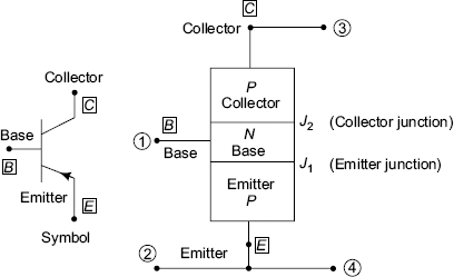
FIGURE 3.2 P-N-P transistor symbol and material representation of P-N-P transitor
For a transistor to act as an amplifying device, it requires that the base-emitter junction J1 is forward biased and the base-collector junction J2 is reverse biased. The arrow on the emitter terminal of the transistor symbols, shows the direction of forward current when the emitter base junction is forward biased.
Transistor device can be connected in three basic modes or configurations that are known as (1) common emitter transistor configuration (CE Transistor operation), (2) common base transistor configuration (CB transistor operation) and (3) common collector transistor configuration (CC transistor operation). In each mode, one of the three terminals of the transistor is grounded and the other two form input and output terminals. Thus, transistor is operated as a four terminal or a two-port network. For instance, in common emitter configuration the emitter terminal is grounded and the input is applied between base and emitter forming the input port. Output is obtained between collector and emitter terminals, which form the output port. Thus, a transistor is considered as a two-port network as shown in the Figures 3.3, 3.4 and 3.5.
Common Emitter Transistor Configuration

FIGURE 3.3 Common emitter connected transistor (CE transistor configuration)
Common Base Transistor Configuration

FIGURE 3.4 Common base connected (operated) transistor (CB tramsistor configuration)
Common Collector Transistor Configuration

FIGURE 3.5 Common collector connected transistor (CC transistor configuration)
For an N-P-N transistor, emitter region is made up of heavily doped N-material to provide a large enough emitter current IE. The base region is a very thin P-layer region and least doped and is of smaller area of cross-section. The collector region is again an N-layer that is moderately doped. The collector region is larger in area than the emitter and base regions.
Basic Operation
Basically, the bipolar junction transistor (BJT) is used as a two-port network or as a four terminal network and functions as an amplifying device along with other applications. The name for the transistor device itself is an acronym formed from the two words transfer + resistor = transistor, which will be clear in the course of discussion of the concept of working of the transistor as an amplifying device.
For achieving different levels of resistance, say, low resistance at the input port, the input junction of the transistor is to be forward biased and to achieve larger resistance at the output port of the transistor output junction is to be reverse biased. These different levels of resistances at the input and output ports of the transistor contribute to the amplifying action of the transistor. Thus, for the transistor to act as an amplifying device, there is need for biasing the input (emitter junction) and output (collector junction) junctions of the transistor.
The transistor is known as bipolar junction transistor (BJT), since both electrons and holes participate in the device conduction mechanism to contribute to the flow of various currents through the device, thus is, the operation of the device.
For a transistor to function as an amplifying device the input junction called as the emitter junction J1 of the transistor is to be forward biased (D.C. source used for this purpose is known as bias voltage) by a voltage and the output junction, the collector junction J2 is to be reverse biased by a voltage. Consider common emitter operated transistor with forward bias VBE to the input junction J1 for the input diode between base and emitter and reverse bias VCE to the output junction J2 for the output diode between base and the collector of the NPN transistor as shown in Figs. 3.6–3.9. (Concept of virtual diodes is introduced for clarity of understanding of device operation.)
When the forward bias VBE is increased, there are two forces that act on the majority carrier electrons in the N-material emitter of the N-P-N transistor. Force FVBE = e. VBE due to the forward bias pushes the electrons towards the junction, thereby reducing the depletion region about the input diode junction J1 (of the input diode) between base and emitter regions of the transistor. The negative immobile ion charge at the junction J1 in the P-material base region due to the contact voltage (or built-in voltage or barrier potential VB) V0 tries to restrain the entry of electrons with a force VV0 = e V V0 as long as the barrier potential V0 is not reduced. Once the forward bias VBE overcomes the opposing affect of contact potential; that is, when the actual junction potential (V0 – VBE) at that instant is less than the barrier potential V0; electrons are injected from the emitter into the P-material base region of the transistor.
The movement of the injected minority carrier electrons from the emitter into the base region to the other end of the base area is by diffusion, because of the charge gradient among the injected electrons and the small quantity of originally existing minority carrier electrons in the P-type base material. During this course of journey some electrons recombine with the holes in the base material. These recombinations are less in number, because of the small area of cross-section of the base material and light doping; the numbers of available holes for recombinations are less For a good N-P-N transistor, almost all the electrons injected from the emitter into the base will be collected and IC is preferable to be almost equal to IE. Hence, the P-type base region should be narrow and the electron lifetime should be long. The lost holes in recombinations are supplemented by positive terminus of VBE contributing to the very small magnitude of the base current IB; which is shown as entering into the base of the transistor. Once the injected electrons are at the junction J2 of the output diode, the electrons enter the collector region because of the reverse bias to the output junction J2 (of the output diode) and then are pulled onto the positive of the supply voltage VCE. So, the collector current IC is into the collector terminal (direction of the conventional collector current IC is opposite in direction to the movement of electrons out of the collector terminal). Also, it can be seen from the directions of flow of the base current and the collector current through the emitter terminal as the emitter current IE; which is the sum of the base current and the collector current.
Mathematically, |IE| = |IB + IC|
Thus, mathematically IE is expressed as above, for the N-P-N transistor under discussion.

FIGURE 3.6 CE transistor with biasing voltages
For understanding the physical operation of the N-P-N transistor, the transistor is considered to be the virtual connection of two semiconductor diodes (i.e. one diode, the input diode between emitter and base and the second diode, the output diode between base and the collector) back to back. For a transistor to be operated as an amplifying device, the input diode (N-P diode) between base and emitter with junction J1 is to be forward biased and the output P-N diode between base and collector with junction J2 is to be reverse biased. Voltage VBE forward biases the input diode and the voltage VCE reverse biases the output diode as shown in Fig. 3.7 (wherein the concept of virtual base through two diodes back to back for an N-P-N transistor is visualised).
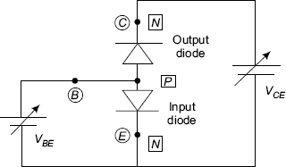
FIGURE 3.7 Diode representations for N-P-N transistor (virtual)
N-P-N Transistor Working
Figs. 3.8 and 3.9 show the N-P-N transistor with biasing voltages for the common emitter mode operation to understand the device operation. The forward bias VBE (D.C. source VBB is used to provide the forward bias VBE) between emitter and base regions for the junction J1 (of the virtual input diode) reduces the depletion region (transition region or space charge region) width WEB about the junction J1. The forward bias causes the movement of majority carrier electrons from the emitter into base region.

FIGURE 3.8 Common emitter transistor circuit (for understanding the principle of working)

FIGURE 3.9 CE transistor with biasing voltages for understanding the principle of working
Emitter region is heavily doped and so large numbers of electrons are injected from the emitter into the base region. That is how the emitter is considered as the source of electrons. At the same time, holes move from the base into the emitter region. The numbers of holes that move from the base into the emitter are deliberately made less, because of small area of cross-section of the base and its light doping. So, the emitter current IE is almost contributed by the injected electrons from the emitter into the base region and further proceeding towards the collector region.
There is a concentration gradient between injected electrons from the N-type emitter into the base region and the small number of originally existing minority carrier electrons in the P-material base. As the electrons diffuse through the base material, some electrons recombine with the holes. The number of recombinations are deliberately made less by reducing the area of the base and its light doping concentrations, so that the probability of recombinations is less. The lost holes due to recombination are supplemented by the positive terminal of VBE and enter through the base lead contributing to the base current IB due to the holes entering the base region. The remaining electrons enter the collector region and are collected by the collector due to the positive nature of the reverse bias voltage VCE across the junction J2 (of the virtual output diode). The collector area is much larger than the emitter area to reduce the junction heating due to the power dissipation at the collector junction.
The Current Components through the Transistor
The current components through the transistor device and external paths and also the depletion region widths to illustrate base width modulation are shown in the Fig. 3.10
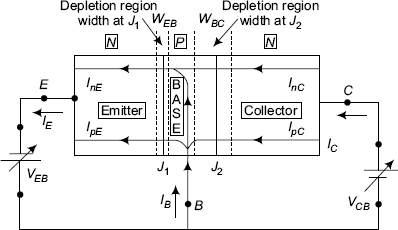
FIGURE 3.10 Various current components and depletion region widths to illustrate base width modulation in a N-P-N transistor
The transistor operates in the active region when the base -emitter junction J1 is forward biased and the base-collector junction J2 is reverse biased irrespective of the transistor configuration. The emitter current IE is the sum of majority carrier electron current and the minority carrier hole current in the N-P-N transistor as shown in the Fig. 3.10.
All the electrons that cross the emitter -base junction do not reach the collector, since there are some recombinations with holes in the base region and the remainder enters the collector and the collector current component is INC. There is a small minority carrier current due to reverse bias of the base-collector junction designated as the current IC0.
The net collector current will be IC = (IC0 – INC); if IE is not equal to zero. When IE = 0, the collector current IC = IC0; since INC representing the injected carrier current is zero, since IE = 0.
Emitter injection efficiency as per definition,
Base width Modulation and Early Effect
The bias voltage VEB forward biases the input junction J1 of the N-P-N transistor and the bias voltage VCB reverse biases the output junction so that the transistor operates as an amplifying device. The reverse biased base to collector junction produces depletion regions into the base and collector regions with widths inversely proportional to the doping levels. Thus, the spread of the transition regions or the space charge regions into the base region is much more into the base region than into the collector region, which becomes relatively negligible. Also, almost all the depletion region width spread is in the base region only. This reduces the effective width of the base region proportional to the applied reverse potential or bias voltage across base-collector junction J2. These types of changes in the effective base width with variations in the reverse biasing voltages to the output junction of the transistor is known as base width modulation as shown in Fig. 3.10.
The reduction in the effective base width with increase in reverse bias reduces the recombination probabilities of holes and electrons in the base region resulting in the decrease of base current IB and consequent increase in the collector current IC. This is called as early effect. The upward slope in the output characteristics of transistors is due to the early effect that will be clear in later discussions. But for the early effect, the collector current should be independent of the reverse bias to the output junction, since the charge carrier reach the collector falling through a potential valley at the output junction which are further explained at the explanation for obtaining the transistor output characteristics.
3.2 Transistor Characteristics
To know the electrical behaviours of the transistor and determine the application or use of the transistor in the practical electronic circuits, the following setup shown in the Fig. 3.11 is used. The curves that represent the variations of currents with respect to voltages at the input and the output ports are known as the static characteristics of the devices. The characteristics between the parameters VCE and IB at the input port, maintaining VCE constant are called the input characteristics. The characteristics between the parameters VCE and IC those at the output port, maintaining IB constant are called the output characteristics.
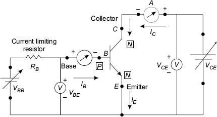
FIGURE 3.11 Common emitter transistor circuit to obtain input and output characteristics
Input Characteristics
As can be seen from the curves, the input characteristics are nothing but the forward characteristics of the input junction P-N diode. Input characteristics of a common emitter transistor are between VBE and IB (the input port parameters of the CE transistor) for constant values of VCE. To start with a particular value of collector supply voltage VCE or VCC is applied at the output port for example 5 volts. The magnitudes of input voltage VBE and current IB are measured for various values of VBE. Now, VCE is changed to say 10 volts and the magnitudes of VbE and IB are measured and tabulated. Using the observed data the input characteristics of the transistor can be drawn that look like the curves in the Fig. 3.12.

FIGURE 3.12 Input characteristic of common emitter transistor
Thus, up to and below Vγ (cut in voltage) of the input diode or the emitter junction, the base current IB is virtually zero. From Vγ onwards, the base-emitter diode is progressively forward biased and the input current starts rising slowly first and rapidly due to the exponential relation between voltage and current. As can be seen from the curves, the input characteristics are nothing but the forward characteristics of the P-N diode.
For the higher VCE (10 volts) the reverse bias on the output junction, the collector junction increases. The increase in reverse potential increases the depletion region widths in both base and collector regions about the junction. The increase in depletion width is more on the base side than on the collector side, since the base is much less doped than the collector region. To wit, the spread of the depletion width is mostly on the base side and literally negligible on the collector side. Thus, the effective base width decreases and the effective base resistance increase causing a decrease in base current. The field between emitter and base increases, pulling more electrons from the emitter region. Thus, increasing the emitter current as well as collector current. That is the reason why, base current decreases and collector current increases.
As is observed in the characteristics, this variation of base current due to variation of reverse bias on the base-collector junction is due to base-width modulation or early effect.
The input characteristics show that for higher VCE, the curve is pushed to the left or for a given VBE; IB1 for VCE1 is less than IB2 for VCE2; where VCE2 is greater than VCE1.
Output Characteristics
Using the experimental setup shown in the Fig. 3.11, the transistor output characteristics are obtained. Initially, with IB = 0 microamperes (Zero VBE), varying VCE resulting collector current IC magnitudes are observed. Now the collector current will be simply equal to ICO, the saturation current, because the forward bias VBE to the emitter junction is zero. VBE is adjusted to choose a convenient value of IB and is to be kept constant. VCE is varied in steps and the pairs of values of VCE and IC are observed and tabulated. For different sets of constant values of IB, variations in IC for varying magnitudes of VCE are observed and tabulated. Plotting the observed data, a family of curves known as the Transistor output characteristics between VCE and IC for constant values of IB can be obtained as shown in the Fig. 3.13
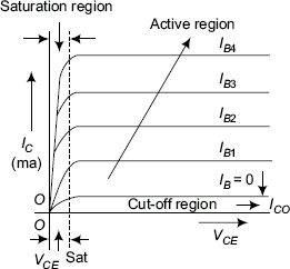
FIGURE 3.13 Common emitter transistor output characteristics
Interpretation of Output Characteristics
The output characteristics show that there are three distinct regions:
(1) Active region, (2) Cut off region, and (3) Saturation region.
In the cut-off region, the collector current IC is almost zero and is equal to ICEO; the reverse saturation current between emitter and collector with base open circuited. In this region, the transistor acts as a open switch.
In the saturation region, there is a large collector current (IC) variation for small region in which VCE changes very much less. VCE is of the order of a few tenths of a volt and is called as VCE sat. In this region the transistor acts as a closed switch with virtually zero voltage drop across it. The resistance rCE sat in this saturation region is of the order of a few ohms.
In the active region, with increase in IB, the output characteristics shift up. For a given IB with VCE = 0 volts, IC = 0 mA. As VCE increases, IC increases up to knee points and beyond that knee region, the collector current (IC) increases with VCE with a small upward rise. In fact, the current should have been constant but for early effect.
3.3 Small Signal Low Frequency Amplifier, h-Parameters
An amplifier can be considered as a two-port (four-terminal) network, with conveniently defined parameters, which find practical use. For instance, for a transistor circuit design, the hybrid parameters are useful. Transistor is basically a current amplifier but natural sources are voltage type in nature. So, the following expressions are used to represent the input and output relations.

FIGURE 3.13-A Transistor as two-port network
Considering the transistor as shown in the Fig. 3.13 A
Putting the above equations in matrix form
As can be seen later, the parameters h11, h12, h21 and h22 do not have the same dimensions; h-parameters are known as hybrid parameters.
From the above equation, by applying some boundary conditions, h-parameters can be obtained.
If in equation (3.1) and (3.2), V2 is made zero, that is, output port is short-circuited
h11 has the dimensions of a resistance and pertains to the input port and it can be termed input resistance hi represented by hi = ![]() The unit of input resistance hi is ohms.
The unit of input resistance hi is ohms.
In the same way,
h21 is a dimensionless quantity representing the ratio of output current to input current or current gain. This is represented by hf = ![]() and is called forward current gain hf. It is a dimensionless quantity.
and is called forward current gain hf. It is a dimensionless quantity.
Now by making I1 = 0 or open circuiting the input port, two more parameters are obtained as following:
h12 is a reverse voltage transfer ratio and is named hr. It is a dimensionless quantity and gives an idea as to the voltage that appears across the input port. This in fact, represents the unwanted voltage transfer from the output to the input, since amplifiers should be preferably unilateral in transfer of energy from input into the output ports, but not the other way round.
h22 represents the admittance of the output port and is designated as output conductance, ho. ho is measured in mhos or siemens.
Thus, as the h-parameters possess a mixture of units, they are known as hybrid parameters.
When applied to analysis of amplifiers with alternating signals V2 = 0 and I1 = 0 represent constant D.C. values of voltage at the output port and current at the input port. Since the transistor characteristics are not entirely linear, the values of the h-parameters change from point to point and are defined over small linearised regions and hence are called small signal parameters.
In this context, input resistance
Forward current gain
Reverse voltage transfer ratio
Output conductance
Transistor amplifiers can have three configurations with any one of the terminals grounded. The other two terminals forming the input and output terminals subject to the original definition.
So, three sets of h-parameters are obtained with the second subscript to the h-parameters, designating the grounded terminal.
So, for CE configuration of transistor the h-parameters become hie; hfe; hre and hoe.
For common base configuration these parameters are hib; hfb; hrb and hob.
For common collector configuration, the h-parameters are hic; hfc; hrc and hoc.
All these parameters can be determined from the static characteristics of the transistor.
The different sets of parameters are interrelated and inter convertible. For instance,

where
and using →

or
Similarly,
or
For CC parameters
híc and hoc are equal to hie and hoe, respectively.
Between CE, CC and CB as per chosen directions of positive and negative polarities, CE configuration is considered to be an inverting voltage amplifier, whereas for the same chosen polarities, CB and CC configurations form non-inverting amplifiers.
Common emitter configuration has input impedance hie of the order of 1 K Ohm and output impedance ![]() of the order of 40 K ohms.
of the order of 40 K ohms.
For common base configuration the input impedance hib will be of the order of a few ohms 10 to 20 ohms and has output impedance ![]() of the order of 2 M Ohms.
of the order of 2 M Ohms.
CB configuration has a reasonable voltage gain but current gain hfb or α is less than unity (Ic (output current) < Ie (input current)).
CC configuration has a current gain of hfc = (1 + hfe) but the voltage gain is less than unity (as will be explained later it forms the voltage series negative feedback amplifier with feedback factor
Determination of Reverse Voltage Transfer Ratio hre, and RIN or hie
Input characteristics to find out (Rin or hie) are shown in the Fig. 3.14.
Input resistance Rin or hie of the common emitter transistor is defined from the forward resistance of the input diode as ![]() and can be determined from the input characteristics as shown in the Fig. 3.14.
and can be determined from the input characteristics as shown in the Fig. 3.14.

FIGURE 3.14 Input characteristic of common emitter transistor to determine hie or Rin.
For VBE1, there is a corresponding IB1, and for another base-emitter voltage VBE2; IB2 is the base current.
Therefore VB E2 − VB E1 = ΔVB E
And corresponding increment in base current ∆IB = IB2 – IB1.
This is the slope of the input characteristic for a specific value of VCE.

Determination of (Rin or hie)
Determination of the Reverse Voltage Transfer Ratio hre
A constant IB line is drawn on the input characteristics of CE transistor of Fig. 3.14A; to determine the reverse voltage transfer ratio hre defined as following. hre is the ratio of change in base voltage VBE to change in collector voltage VCE for a constant IB.
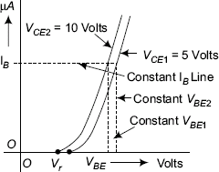
FIGURE 3.14A Input characteristic of common emitter transistor to (determine hre)
Determination of Current Gain hfe and Rout = 1/hoe and gm from Output Characteristics:

FIGURE 3.15 Transistor output characteristics (to determine hfe and hoe)
Determination of the Current Gain β or hfe of the Common Emitter Transistor
β, the incremental current gain is also called hfe and is obtained in the following way.
For a common emitter operated transistor, for a given VCE; the ratio of incremental collector current ∆IC and incremental base current ∆IB is defined as the small signal forward current gain β or hfe.
Forward current gain β of a common emitter (CE) operated transistor is defined as following
Forward current gain β of a common Emitter (CE) transistor can be determined from the
Data from the Common emitter transistor output characteristics of Fig. 3.15 to determine β is as follows.
IB2 = 200 μA; IC2 = 20 mA IB1 = 100 μA; IC1 = 10 mA
ΔIC = (20 − 10) 10−3 = 10 mA
ΔIB = (200−100) 10−6 = 100 μA
Current gain of common emitter transistor ![]()
Determination of the Output Resistance Rout = 1/hoe of the Transistor
Rout is defined as the slope of VCE versus IC characteristic for a constant IB.
Thus,
So,
Assuming the following data from common emitter transistor output characteristics, output conductance and output resistance are calculated as given below.

gm is by definition
As

3.3 Common Base Mode Transistor
In common base transistor configuration, base terminal is grounded and forms the common terminal for both input and output ports. Thus, when the base terminal of the transistor (BJT) is common to both the input and output ports, the mode of operation of the transistor is called the common base mode of operation as shown in Fig. 3.16.

FIGURE 3.16 Common base transistor configuration
For the transistor to be in the active region of its output characteristics, it requires that the emitter junction, the input junction, that is, the emitter-base junction is to be forward biased by VEB and the output or collector-base junction is reverse biased by VCB as shown in the Fig. 3.16.
As seen from the Fig. 3.16 the input current is the emitter current IE and the output current is the collector current IC. The current through the base lead is IB and |IB| = |IE – IC |. The current gain α of the common base operated transistor is defined as the ratio of the change in collector current ∆IC to the change in emitter current ∆IE with constant collector to base voltage VCB.
Current gain
Current gain
Since the emitter current is greater than the collector current, the current gain of common base operated transistor is always less than unity and as the difference in magnitude between the emitter and collector current (IE – IC = IB) is very small, the current gain α (alpha) of the common base transistor is less than one and always close to unity.
Input Characteristics of CB Transistor
For any transistor configuration, whether it is common emitter (CE) configuration or common collector (CC) configuration or common base (CB) configuration; the input and the output characteristics are drawn between voltage and currents. For the input characteristics, the output voltage is kept constant. For the output characteristics the input current is kept constant.
The input characteristics of common base (CB) transistor are thus between VEB and IE; the input voltage and current variations maintaining constant VCB, the reverse bias to the collector junction. The experimental setup to obtain the data for input and output characteristics is shown in the Fig. 3.16 and the input and output characteristics are shown in Figures 3.17 and 3.18, respectively.
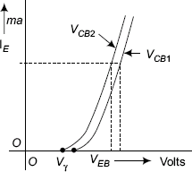
FIGURE 3.17 Input characteristics of common base (CB) transistor
The input characteristic of any transistor configuration is similar to a forward biased diode. The input characteristic of this common base transistor is nothing but that of the forward biased emitter-base diode. For a given VCB, as VEB increases, beyond the cut-in voltage Vγ the emitter current IE increases just like in a forward biased diode as shown in the Fig. 3.17. After passing the cut-in voltage, Vγ, for small changes of VEB, large changes of IE occurs.
For a constant VEB, the increasing reverse bias voltage, VCB can increase the emitter current IE.; when the early effect comes into play. So, the knee voltage or the cut-in voltage or the threshold voltage for conduction of the emitter diode, lowers and large changes in IE can be obtained at lower VEB. This can be seen on the input characteristics that for a higher value of VCB2; the characteristic moves to the left of VCB1 characteristic. Due to base width modulation or early effect, when VCB is more IE increases due to increased field at the collector junction and it requires less VEB to draw the same emitter current IE and thus the curve for VCB2 moves to the left of that for VCB1.
The slope of VEB versus IE characteristic (input characteristic) is the input resistance represented by hib of the common base operated transistor. The input resistance of the common base transistor is defined as following:
The input resistance hib will be of the order of a few ohms, that is, about 10 to 20 ohms. This is very low when compared to the input resistance hie of CE transistor, which is typically 1 KΩ. The reason for this difference in magnitudes of the input resistances is clear from the following equation:
Since IB, the base current is a few orders less than the emitter current IE; the input resistance hib of common base transistor is so many orders less than hie. Also, the magnitudes of IE and IB in the expressions for the input resistances of the common emitter and common base configurations of the transistor confirm the same.
Output Characteristics of Common Base Transistor
For a given magnitude of emitter current IE the graph between the output parameters, the collector current IC and VCB is called the output characteristic and a family of output characteristics are obtained for different values of IE as shown in the following Fig. 3.18.
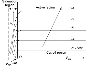
FIGURE 3.18 Output characteristics of CB transistor
It is already familiar that for a given emitter current IE; the forward biased input junction, a small current IB goes to the base and the remaining current goes to the collector as the collector current IC; according to the equation IE = – (IB + IC).
The region between the output characteristic for IE1 = 0 mA and VCB axis on the CB transistor output characteristics is the cut-off region. The magnitude of collector current is ICB0 which is negligibly small, that is, of the order of a few nanoamperes for silicon device and is of the order of a few microamperes for a germanium device under the situation of reverse bias to collector junction. The output characteristics resemble the reverse biased diode characteristic with reorientation of the quadrant of appearance and the parameters.
When the collector terminal is open, the entire emitter current IE goes to the base and the collector current IC = 0. When VCB is zero, the electrons (for N-P-N Transistor) that cross the base region face a field at collector-to-base junction J2 that neither opposes nor aids the electrons will allow all the electrons to continue their journey into the collector circuit and the collector current IC for a given emitter current IE becomes maximum even at the starting point of the characteristic, that is, for VCB = 0 volts.
Now, if VCB increases, the base width modulation occurs and a very slight increase in the collector current IC is observed. The reason for this virtually constant IC with variations in VCB is that the electrons with reverse bias at the collector face an accelerating potential and they move with constant velocities or experience acceleration but the quantum of collector current IC changes by a very little magnitude.
The relation between the collector current and the emitter current is defined according to the following equation
where IC0 is the reverse saturation current which is ≅ 0 with IE = 0 mA
![]()
α is called as the forward current gain of common base transistor.
As compared to the CE transistor configuration, the phenomenon of early effect is less prominent in CB transistor operation, since the forward current gain alpha α is less than unity and change in collector current IC is negligibly small.
The slope of the collector current IC versus VCB characteristic (output characteristic) is almost zero and hence the output impedance of the CB transistor runs into megaohms.
Grounding of the base terminal produces perfect isolation between the input and the output ports, since it acts as a shield between emitter and collector and there is no common path between the two ports. In other words, the emitter to collector inter electrode capacitance virtually becomes zero.
The very low input impedance of the transistor CB configuration makes it unsuitable to be driven by non-ideal voltage sources (whose source impedance is not negligible). All practical voltage sources are non-ideal. But this common base mode transistor can be used with current sources, but natural current sources are rare and so the common base configuration finds less practical application.
The use of common base transistor in high frequency applications is appreciable because of its ability to provide perfect isolation between the input and output ports of the transistor.
3.4 High Frequency Linear Models
As the common emitter circuit is the most important practical configuration, common emitter transistor model valid at high frequencies is discussed. The circuit is very accurate and is called hybrid-π or Giacoletto model as shown in the Fig. 3.19. The circuit is applicable for both low and high frequencies.

FIGURE 3.19 Hybrid-π equivalent circuit of CE transistor considered at high frequencies
Hybrid- π or Giacoletto Model
Analysis of circuits using this hybrid-π model is not too difficult and gives results, which are in excellent agreement with experiment at all frequencies for which the transistor gives reasonable amplification. All parameters (resistances and capacitances) in this model are assumed to be independent of frequency.
Elements of the Model
rbb′: |
The internal point (B′) is the effective base point. |
rb′e: |
The resistance rb′e represents the resistance of the forward biased base to emitter junction, the emitter junction of the transistor. |
Cb′e: |
The capacitance Ce or Cb′e is placed in parallel with rb′e to account for the input junction, that is, the emitter junction diffusion capacitance accounting for the excess minority carrier storage in the base. This is the capacitance of the emitter to base forward biased junction. |
rb′c: |
It represents the resistance of the reverse biased collector to base junction. |
Cb′c or Cc: |
It represents the capacitance of the reverse biased collector to base junction. (Also known as the output junction or the collector junction capacitance.) |
gm Vb′e: |
Small changes in the voltage Vb′e across the emitter junction finally results in small signal collector current gmVb′e. This effect is accounted as current generator gmVb′e (when collector is shorted to emitter) as shown in Fig. 3.19. |
rce, = 1 /gce: |
The conductance between C and E is gce. |
Some typical hybrid-π parameter values of common emitter transistor at high frequencies:
gm |
= |
50 ma/v or 50,000 µΩ |
rbb′ |
= |
100 Ω |
rb′e |
= |
1000 Ω |
Cb′e |
= |
100 pf |
rb′c |
= |
3 × 10⁶ Ω |
Cb′c |
= |
2 pf |
rce |
= |
100,000 Ω |
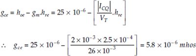
Determination of Hybrid- π Parameters
Manufacturers supply data that characterise the transistors. Usually, not all of the hybrid-π parameters are given. The determinations of hybrid-π parameters from the commonly published data or from quantities that can be easily determined are considered.
1. Determination of transconductance (gm)
In the linear region for small signals, gm is given by,
At temperature
Transconductance gm can be easily found from the D.C. or Quiescent operating current ICQ decided with the class of operation of amplifiers and the operating temperature T.
2. Determination of input conductance (gb′e) The hybrid-π model valid at low frequencies is shown in Fig. 3.19A, where all capacitances are negligible.
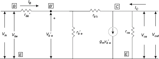
FIGURE 3.19A Hybrid-π equivalent circuit of transistor considered at low frequency
From the typical values of the circuit components of common emitter transistor at high frequencies, rb′c >> rb′e. Hence, Ib flows into rb′e and hence Vb′e = rb′e.Ib.
The short circuit collector current IC is gmVb′e.
Therefore, IC = gm.Vb′e = gm.Ib.rb′e
The short circuit current gain hfe is defined by
Manufacturers usually specify ßo = hfe
3. Determination of rbb′ From Fig. 3.19A, the input resistance with output shorted is hie.
Under these conditions rb′e is in parallel with rb′c
∴ rb′e || rb′C ≅ rb′e since, rb′C 〉〉 rb′e
From Fig. 3.19A with output shorted
4. Determination of feedback conductance (gb′c) With the input open-circuited, hre is defined as the reverse voltage gain with Ib = 0.
∴ hre.(rb′c + rb′e) = rb′e
∴ hre.rb′c = rb′e(1 − hre)
Since hre ≅ 10−4 that is, hre 〈〈 1, Then, (1 − hre) ≅ 1
Therefore, hre.rb′c = rb′e
When ![]() which means that rb′c 〉〉 rb′e that is, rb′c will have a magnitude of the order of megaohms.
which means that rb′c 〉〉 rb′e that is, rb′c will have a magnitude of the order of megaohms.
5. Determination of output conductance (gce) With the input open-circuited, the conductance is defined as hoe for Ib = 0
With Ib = 0; Vb′e = hreVce. Substituting this in the above equation
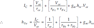
As rb′c 〉〉 rb′e ∴ (rb′c + rb′E) ≅ rb′c
![]()
using gm = gb′e .hre from equation (3.25) in the above equation,
using ![]() in the above equation,
in the above equation,
|
|
∴ |
hoe = gce + gb′c + hfe.gb′c |
∴ |
hoe = gce + gb′c (1 + hfe) ≡ gce + gb′c.hfe |
∴ |
gce = hoe − hfe.gb′c |
Also, |
hoe = gce + gb−c + gm.hre |
|
|
i.e. |
goe = hoe − gm.hre (3.28) |
6. Determination of Cb′c The value of the capacitance of the reverse biased collector-to-base function Cob is often specified in the manufacture’s transistor’s data. Cb’c = Cob is the capacitance measured between the collector and base leads with the emitter lead open circuited (for signal frequencies) Cb’c = Cob.
7. Determination of Cb′e or Ce Experimentally Cb′e is determined from a measurement of FT, the frequency at which the common emitter short circuit current gain drops to unity.
Validity of Hybrid-π Model
The hybrid-π model is valid under dynamic conditions, when the rate of change of Vbe is small enough so that the base incremental current ∆Ib is also small. It was also proved that the hybrid-π model is valid for frequencies up to approximately ![]() where fT is the frequency at which current gain of an amplifier is unity. fT is also known as unity gain frequency. fT incidentally is the gain-bandwidth product of an amplifier, that will be explained more later.
where fT is the frequency at which current gain of an amplifier is unity. fT is also known as unity gain frequency. fT incidentally is the gain-bandwidth product of an amplifier, that will be explained more later.
Example A junction transistor is to operate at the following operating point ICQ = 2 mA, VCEQ = 20v and IBQ = 20μA. The following values for this operating point are the specifications of the transistor. ßO = 100; fT = 50 MHz; C0b = 3 pf; hie = 1.4 KΩ; hre = 2.5 × 10⁻⁴; h0e = 25 μ mhos. Determine the hybrid-π model parameters of the transistor. Assume that the operating temperature is 300 K.
Solution


- rbb′ = hie − rb′e = 1400 − 1300 = 100 ohms

- Cb′c = Cob = 3.pf

3.5 Field Effect Transistor
While a transistor (BJT-bipolar junction transistor) is a bipolar device and basically a current-operated device, a junction field effect transistor (JFET or simply FET) as the name itself suggests is a voltage-operated device. These terms are derived from the device operations. These terms indicate the basic difference between BJTs and FETs.
The control electrode current is high with the forward biased input junction of BJT, whereas, the input electrode current of FET devices is negligibly small. The transistor has another disadvantage that its input impedance is low and requires ideal voltage sources for driving it. The other alternative is to use a buffer amplifier in the form of emitter follower as an impedance matching network.
The JFET is basically reverse biased at the input port and has theoretically infinite input impedance. Thus, it acts as an ideal front end connecting circuit in practical applications. The currents through the field effect transistor are due to the movement of majority carriers. Hence, the FET is a unipolar device and a voltage variable resistance made to operate as an amplifier.
When, very high input resistance amplifier stage is to be designed, FET amplifier stage is preferred over bipolar transistor amplifier stage.
Transistors are nonlinear devices as evident from the device characteristics. Transistor operation is considered as linear for small signal operations of amplifiers.
There are two types of FETs. The JFETs also called Junction gate FET and the MOSFETs (Metal Oxide Semiconductor Field Effect Transistors) are also called Insulated Gate FET (IGFET) from the structure and functioning of MOSFET devices as seen further.
As mentioned earlier, the field effect transistor (FET) is unipolar and has only one type of current carriers, the majority carriers for electrical conduction of the device. If the current carriers are electrons FET is called an N-Channel JFET. The complement of this is P-Channel JFET having holes as current carriers. The schematic symbols of N-Channel FET and P-Channel FET are shown in Fig. 3.20. The arrow head on gate electrode indicates the direction of current when the gate-source junction is forward biased.)

FIGURE 3.20 Field effect transistors
Just like a transistor, FET device also has three terminals the source, the gate and the drain (similar to emitter, base and collector electrodes of a transistor). But in a FET, the source and drain are interchangeable as opposed to the transistor device, where, the emitter and collector cannot be interchanged.
In FET devices, there are no separate input and output junctions as in the case of transistors. N-channel FET has N-type semiconductor bar. Drain terminal is at the upper end and source terminal is at lower end of the N-type bar. Here, between drain and source, an N-channel exists, which is called a channel. As is shown in Fig. 3.21, on the other two sides of the N-type of semiconductor slab, P-materials are formed and these two P-material sides are joined together to form the gate electrode.

FIGURE 3.21 N-channel field effect transistor
Thus, on two sides of the slab, there are P-N junctions, though the two P-regions are joined together to form one electrode, the gate. Voltage VGS or VGG is connected between gate and source of N-Channel field effect transistor with negative of the voltage source connected to the gate electrode and positive to the source terminal. The two P-N Junctions between the gate and the source are thus reverse biased by the D.C. voltage VGS or VGG. The gate of the N-Channel FET device draws negligible current, that is IG = 0. So, FET is a voltage-controlled device.
D.C. voltage VDS or VDD is connected between the drain and the source terminals of the FET device. The majority carriers in the N-channel JFET device are electrons and the active output terminal is the drain. The positive of the D.C. voltage source VDS or VDD is connected to the drain terminal and the negative of the D.C. source is connected to the source terminal as shown in the Fig. 3.21. Electrons flow from drain to source in the output circuit between drain and the source for various values of VDS. The conventional drain current ID flows from the positive terminal of VDS or VDD through the device from the drain to the source and then completes the path to the negative terminal of VDS as shown in the Fig. 3.21.
Initially, when VGS = 0 volts and VDS = 0 volts, the depletion region widths (of unbiased junctions) about the junctions are uniform. With the increases in voltages, VDS for different constant values of VGS, the situation is that the reverse bias is more towards drain end than the source end at the two P-N junctions in the device (the varying magnitudes of the reverse biases is due to the flow of the drain current ID through the device channel across increased areas of cross-sections of the channel from the source to the drain, thus producing different voltage drops across the channel). These varying reverse biases cause varying magnitudes of depletion region widths about the two junctions. Increased reverse bias magnitudes from source to drain cause increased depletion region widths towards the drain as shown in the Fig. 3.21.
With the drain shorted to the source and a negative voltage applied between gate and source two reverse biased junctions appear on both sides of the gate and depletion regions spread into the slab. As the reverse voltage increases, the conducting area of the channel is reduced. The drain current decreases with increasing reverse bias and when it is high enough the channel virtually closes and small reverse current flows. This is the condition when ID is almost zero and the channel is pinched off (cut off with VDS = 0 volts).
3.6 FET Characteristics
Using the experimental setup of Fig. 3.21A; the basic properties of a typical FET are illustrated by the device characteristics as shown in the Fig. 3.22.
Output characteristics of the FET device are between the drain to source voltage VDS and drain current ID for a set of constant gate to source voltages VGS. Initially, voltage VGS is kept at zero volts. It is kept constant. Then varying the voltage VDS in increments, the corresponding incremental values of ID are tabulated. A family of output characteristics is obtained for a set of gate to source voltages VGS as shown in the Fig. 3.22. The drain resistance rd can be calculated from the output characteristics in the pinch-off region.

FIGURE 3.21A Experimental setup to obtain FET characteristics
Transfer characteristics of the FET device are between the gate to source voltage VGS and the drain current ID for a set of constant drain to source voltages VDS. Initially, VDS is kept constant, say, at 10 volts. Varying gate to source voltages VGS from 0 to the pinch-off voltage VP (VGS off) of the device in increments (VP is gate voltage when the drain current ID becomes zero), corresponding increments of drain current ID are tabulated. This procedure may be repeated for another constant voltage VDS to obtain another transfer characteristic. The transfer characteristic is drawn as shown in the Fig. 3.26. The Transconductance gm can be calculated from the transfer characteristics.
The amplification factor μ also can be determined from the output characteristics or as the product of gm and rd (μ = gm·rd). These device parameters are defined later. The maximum gain of FET amplifiers is decided by the maximum value of the amplification factor of the device.

FIGURE 3.22 JFET characteristics with different values of pinch-off voltages depending upon the values of VGS
Discussion on the Output Characteristics of FET
VGS is maintained constant at certain values (for example VGS = 0 volts) as shown in the Fig. 3.22. At each constant value of VGS, as VDS is increased up to a few volts drain current ID linearly increases from the origin 0 to A the majority carrier electrons flow from source to drain through the N- type channel and then complete their path through the drain circuit. The channel resistance is uniform and acts as a semiconductor resistor. The channel resistance limits the current. The resistance increases with VDS as shown on the output characteristics of the FET device in the Fig. 3.22. This region from 0 to A on the output characteristics is known as Ohmic region.
For each ![]() , where rd is the drain resistance. In this region of operation, the FET device behaves like a voltage variable resistor (VVR) or voltage dependent resistor (VDR).
, where rd is the drain resistance. In this region of operation, the FET device behaves like a voltage variable resistor (VVR) or voltage dependent resistor (VDR).
For higher values of VDS, the channel resistance becomes non-uniform, during the region A to B on the output characteristic, since the depletion region width changes along the length of the channel from source to drain as shown in the Fig. 3.21. This region is known as Nonlinear region.
At the source end, the depletion region width is minimum and at the drain end it is maximum, because of varying reverse bias voltages (due to varying voltage drops between the source and the drain along the channel region due to the flow of the drain current ID) at the gate-source and gate-drain junctions, respectively that can be seen from the Fig. 3.21. Thus, for each VGS on the drain characteristics, with increasing values of VDS, the magnitudes of the drain current ID increases up to a drain to source voltage VDSP simply known as the pinch-off voltage VP. The drain current starts raising slowly and finally reaches a constant value or ID reaches a saturation value, (where the depletion region widths come closer, but never overlap for the prevention of disappearance of reverse bias to maintain the device operation) above the knee portion from the pinch-off voltage VP as shown in the Fig. 3.22. The region B to C on the output characteristic is the Pinch-off region, the active region for amplifier operation.
When VGS = 0 v, ID will be maximum ever that is reached and it is called drain saturation current IDSS. This is also clear from the following equation.
The relation between ID, IDSS, VGS and VP is given by Shockley’s equation:

For a given VGS, VDS versus ID characteristics (output characteristics) have four regions.
1. Linear region from 0 to A on the output characteristic of the JFET device is known as (voltage dependent resistor, VDR) VDR region or simply Ohmic region.
2. The knee portion from A to B on the JFET output characteristic, in which the device resistance suddenly changes from a low value to a high value exhibits a nonlinear behaviour. This is called as the Nonlinear region.

FIGURE 3.23 JFET characteristics with pinch-off locus

FIGURE 3.24 JFET characteristics with different regions of operation
3. From B to C portion of the JFET output characteristic, the curve is almost parallel to the X-axis (indicating the saturated or constant values of drain current ID) and is known as the Pinch-Off region and the characteristic in this region exhibits a high resistance of the order of a few hundred kilo ohms and it is called as (one of the FET device parameters or constants) drain resistance rd. This device internal resistance is used in the representation of the small signal A.C. equivalent circuit for the analysis of the FET amplifier operation. The pinch-off region also suggests the voltage controlled current source (V C C S) behaviour of the device in practical circuit applications.
4. Beyond the point C, when the voltage VDS becomes large enough to breakdown the junction causing a sudden high rise of drain current, ID. This Breakdown region is never used in practice and so it is not shown on the output characteristics of JFET device.
Determination of the Drain Resistance rd and the Amplification Factor μ The three FET device constants are transconductance gm, drain resistance rd and the amplification factor μ. The following are the definitions with the relation between them.
Transconductance,
Drain Resistance,
Amplification factor
From these definitions…


FIGURE 3.25 Determination of drain resistance rd from output characteristics
The drain resistance rd can be calculated from the JFET output or drain characteristics. Drain resistance is the inverse of the slope of the output characteristic. Drain resistance is the ratio of the increment in drain to source voltage ∆VDS between VDS2 and VDS1 and the corresponding increment in the drain current ∆ID between ID2 and ID1 that are obtained from the graphs. From the characteristics in the Fig. 3.26, it is clear that large change in the drain to source voltage produces a small change in the drain current.
The drain resistance rd is calculated as the ratio of ∆VDS = [(VDS2 – VDS1)] = 20 – 4 = 16 volts to ∆ID = [ID2 – ID1] = 10 – 9.5 = 0.5 mA. So, the drain resistance rd is equal to 32 kilo-ohms.
Transfer Characteristics of the Field Effect Transistor (JFET) (Determination of Transconductance gm) With the voltage VDS across drain and source electrodes of the JFET device kept constant, if VGS is varied from zero to higher negative values, the drain current ID drops from the drain saturation current IDSS to reach almost zero, when VGS is large enough to close the channel at a voltage VP known as VGS off (pinch-off voltage). The device parameters ID, IDSS, VGS and the pinch-off voltage VP are related by Shockley’s expression,
Differentiating the above equation with respect to VGS; expression for gm can be obtained as following,

using the relation
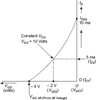
FIGURE 3.26 JFET transfer or mutual characteristic
When VGS = Vp, that is Vas off, ID becomes zero (however, some authors indiscriminately use this VGS off as pinch-off), according to the mathematical expression 3.34. This variation of drain current with variations in VGS for constant value of VDS is shown on the following transfer or mutual characteristics of Fig. 3.26. This characteristic is a nonlinear characteristic as evident from Shockley’s equation 3.34.
The mutual or transfer conductance gm can be calculated from the transfer characteristic or output characteristic of the JFET device.
From the transfer characteristics in Fig. 3.26, the transconductance gm can be determined as the ratio of the increment ∆ID, that is the change in drain current from ID1 to ID 2 which is 5 mA from the graph and the increment in gate voltage ∆VGS that is change in gate voltage from VGS1 to VGS2 which is 2 volts. So, gm is equal to 2.5 milli mhos or milli Siemens. Transconductance is the slope of the transfer characteristic of the FET device.
The amplification factor μ is the product of gm and rd from the definitions of the device constants, as shown previously. In these calculations rd = 32 × 103 ohms and gm = 2.5 milli mhos. Therefore, the amplification factor μ = gm.rd = 32 × 103 × 2.5 × 10−3 = 80. These values for the device constants are only for the sake of illustration of the method of calculations. It can be seen later that maximum gain of a JFET amplifier is limited to the value of amplification factor, μ of the device.
The square law nature of the device transfer characteristic suggests its use in mixer circuits of radio receivers circuits. Once, we know the FET structure, device working and the device parameters, the device application as an amplifier is considered for simple illustration of application of the FET device.
3.7 N-channel FET as an Amplifier
Like a bipolar junction transistor (BJT), a junction field effect transistor JFET is used in amplifier circuits. Amplifier circuits are broadly (1) voltage amplifiers that are small signal amplifiers and (2) power amplifiers that are large signal amplifiers. Consider basic operation of the JFET device as a voltage amplifier using the following circuit in the Fig. 3.27.
Consider the public address system microphone converts the speech or music, that is, the sound energy into electrical signal. Microphone is a transducer that converts the sound energy into electrical signal. Voltage and power amplifiers amplify the electrical signal from the microphone, before the signal is fed to a loud speaker. The speaker converts the amplified electrical signal back into sound energy. The speaker is a transducer that converts electrical signal into sound energy. This amplified sound from the speaker is used practically. This process is discussed in the chapter for amplifier with circuits.
So, amplifiers consider the input and output A.C. signals for amplification. Now, consider the JFET amplifier a small signal amplifier as in Fig. 3.27.
In the basic amplifier circuit shown in the Fig. 3.27, both the D.C. voltages are (1) gate supply voltage or gate to source bias voltage VGG used to set the D.C. voltage VGS (based on the type of the amplifier and its class of operation) and (2) drain supply voltage VDD so as to set the drain current (output current) ID flowing through the FET device to a value such that the voltage across the load resistance RL = ID.RL = VRL is about half the supply voltage VDD to satisfy the Class A operation of the amplifier.
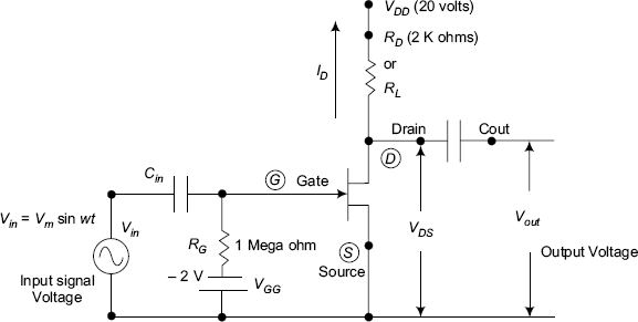
FIGURE 3.27 Basic JFET amplifier circuit
The bias (D.C. voltage) VGG is arranged such that the gate of the N-Channel FET is made negative relative to the source, because the requirement is that gate-channel junction of the N-Channel FET is to be reverse biased so that the input resistance Rin of the FET device is very large, which is an advantage over the BJT devices and facilitates non-ideal driving voltage amplifiers.
The gate-source voltage VGS is established by the bias voltage VGG as shown in the basic amplifier circuit of Fig. 3.27. Because there may be a gate current of only of the order of a few nanoamperes, the voltage across the gate resistor RG (1 × 10−9 × 1 × 106 =10−3 volt) negligibly small and the gate-source voltage VGS is virtually the same as −2 volts. For class A operation of the amplifier. VGS = (1/2). Vp.
Assume the following output characteristics (static characteristics) for the JFET device as shown in Fig. 3.28.

FIGURE 3.28 JFET output characteristics with D.C. load line and the quiscent operating point ‘Q’ for class-A operation of amplifier
The output characteristics of the device can be obtained experimentally or by a curve tracer using a cathode ray oscilloscope. When the JFET device is biased with voltages for the required class of operation of the amplifier, steady state values of the drain current ID and the voltage VDS are related by D.C. load line equation for the amplifier analysis.
Obtaining the D.C. equivalent circuit of the amplifier circuit in Fig. 3.27, the D.C. load line equation can be written as the following (discussed in detail in the amplifier chapter).
The coordinates of the point (X) of the D.C. load line are VDS = 0 volts and ID = (VDD / RL) and the coordinates of the point (Y) of the line are VDS = VDD volts and ID = 0 mA. The D.C. load line can be drawn by joining the two points (X) and (Y).
The drain current IDQ and the voltage VDSQ are obtained by superimposing the D.C. load line on the output characteristics for the required quiescent point operation of the amplifier. If an input signal voltage source, Vin = Vm. sin wt is applied at the input port of the amplifier large variations in ID flowing through the load resistance RL develop the output voltage Vout at the output port. It can be observed that the output voltage will be much greater than the input signal voltage and signal amplification takes place. Gain A of the amplifier is the ratio of the output voltage Vout to the input voltage Vin, provided the voltage gain A is greater than unity.
Comparison between Field Effect Transistor (FET) and Transistor (BJT)
| Junction Field Effect Transistor | Bipolar Junction Transistor |
|---|---|
Device currents are due to the movement of only one type of majority charge carriers. Electrons in N- Channel FET device or holes in P-Channel FET devices. |
Transistor currents are due to the movements of both the majority and minority charge carriers in both N-P-N and P-N-P transistors. |
The input junction between the gate and the source is reverse biased and hence the input resistance of the FET device is very large. This high input resistance of the FET device is an advantage over transistor devices. |
The emitter or the input junction of the transistor is forward biased and hence the input resistance is very low. |
The input signals voltage magnitudes between gate and source control the current through the device. So, it is a voltage controlled current source. |
The input current base current controls the collector current for device operation. It is a current controlled current source. |
Voltage gain is limited to the amplification factor μ of the device, which has low values. So, the amplifier circuits using FET devices have low orders of gain and hence the band width of FET amplifiers are large. |
The amplifier circuits using transistors have large values of current and voltage gains. So, the bandwidth of transistor amplifiers are low. |
Low noise level. |
Noise level is very high. |
3.8 Metal Oxide Semiconductor FET (MOSFET)
Two types of MOSFET are available
- Enchancent mode MOSFET or E-MOSFET
(MOSFET with induced channel)
- Depletion Enhancement modes MOSFET.
(DE MOSFET or MOSFET with built-in channel)
Integrated circuit (IC) technology has revolutionised the semiconductor devices and RLC components fabrication or manufacture in batch processing with small size, and at low cost and phenomenal reduction in size and increase in packaging densities is achieved. Reliability of working is increased, resulting in improved performance.
A silicon wafer of 1 sq. inch size can accommodate up to 400 IC chips of surface area 50 mil by 50 mil. Each chip again can contain 50 separate components to make up 20,000 components in a single wafer. If 10 wafers are used in a single batch processing 2,00,000 components can be manufactured.
Like the JFET, the MOSFET is a lower-power semiconductor device that has high input impedance as first generation electron devices or vacuum tubes and low power requirements of transistors. Both MOSFETs and JFETs have drain, source and gate electrodes in common. Both devices have conduction channel with its resistance controlled by gate to source voltages. There are also P and N-type channel MOSFETs; complementary MOSFETs known as CMOs. FET devices use both. The gate-source path in a JFET is a reverse biased junction by VGS. In a MOSFET, a thin layer of insulating material such as SiO2 is placed over the channel region before the fabrication of the gate electrode. The insulating layer is very thin, which is of the order less than 1 μm. the field produced by gate voltage still penetrates through insulating layer and modulates the conduction of the channel. The input resistance of MOSFET is much higher than that for JFET because of the SiO2 insulation layer between gate and the channel. Input resistance of MOSFET is of the order of 1014 ohms. Since there is an insulator in the input circuit of a MOSFET, the gate potential is not restricted in polarity. There are therefore, two possible modes of operation for MOSFETs. As mentioned earlier, the non-restriction on polarities of gate voltage, enhancement mode and depletion mode of operations are possible.
Manufacturing Process of MOSFET
Considering the fabrication details of the enhancement MOSFET (MOSFET with induced N-type channel) the following steps are involved. The basic MOSFET with N-type channel is formed on a P-type silicon wafer substrate. The source and drain of the MOSFET device with N-type induced channel are N-type islands that are formed or diffused into a lightly doped P-type substrate. Aluminum metal on SiO2 layer (on the substrate) functions as the gate electrode. Thus, the insulating SiO2 layer separates the gate and the conducting (induced) N-type channel. With these basic construction features of the MOSFET device, the device is also known as insulated gate field effect transistor (IGFET).
Step-1 The starting material is a P-type substance or wafer upon which an insulating layer of silicon dioxide SiO2 is grown in the following second step.
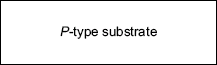
FIGURE 3.29 Base P-type substrate of MOSFET
Step-2 Upon P-type substrate, SiO2 layer is grown as shown in the following Fig. 3.30
SiO2 layer is experimentally grown over the P-type substrate. SiO2 (silicon dioxide) material that has the fundamental property of preventing the diffusion of impurities through it. SiO2 layer thickness is of 0.5 μm (5000Å).
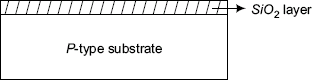
FIGURE 3.30 SiO2 layer formation on P-type substrate
Step-3 Kodak Photo Resist material (KPR) is coated on the SiO2 layer as shown in Fig. 3.31.
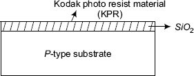
FIGURE 3.31 Kodak Photo Resist material (KPR) coating on SiO2 layer
To perform photolithography-etching process over SiO2 layer to provide two windows for the formation of two islands of N-type material, Kodak Photo Resist material (KPR) is coated over SiO2 layer (KPR is also known as photosensitive material.)
Step-4 A high-resolution photo mask with painted regions at locations 1 and 2 is placed on SiO2 layer as shown in Fig. 3.32.

FIGURE 3.32 Photo mask with two painted regions for forming windows for diffusing N-type materials to form source and drain
A very high-resolution photo mask with two painted regions at 1 and 2 locations over it is placed on the silicon wafers as shown in Fig. 3.32. The painted regions will not allow ultra violet light (UVL) to pass through them (the number of painted areas corresponds to the number of windows and islands to be formed for the device or the circuit component). In this MOSFET device two windows are needed for source and drain island regions, so there are two painted areas on the photo -mask.
Step-5 The photo mask is exposed to ultra violet light radiation as shown in Fig. 3.33.
The photo mask is exposed to ultra violet light (UVL) as shown in Fig. 3.33.
UVL does not pass through the painted regions 1 and 2. UVL passes through the mask over the unpainted areas on 3,4 and 5. KPR over SiO2 layer gets polymerised over the exposed areas for UVL. The KPR over SiO2 in regions 1 and 2 remains as in original situation and are dissolved by using etching solutions easily.

FIGURE 3.33 Photo mask on silicon wafer is exposed to U V light
Step-6 Etching process for the formation of two windows at regions 1 and 2 in Fig. 3.34.
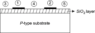
FIGURE 3.34 Etching process for the formation of two windows at regions 1 and 2
Regions 3,4 and 5 on SiO2 layer get polymerised and cannot be dissolved by etching solution. Regions 1 and 2 on SiO2 layer are not polymerised. So, using etching solution, regions 1 and 2 of SiO2 are etched away and two windows are formed and P-type substrate regions are exposed at the two windows areas to facilitate pentavalent material diffusion through them for the formation of N-Type of islands.
Step-7 N-type diffusions through the two windows to form source and drain.
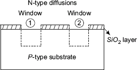
FIGURE 3.35 N-type diffusions through the two windows to form source and drain islands
Through the two windows Pentavalent impurity atoms of phosphorus material are diffused into the dotted window areas and two N- type islands are formed.
Step-8 Formations of N- type source and drain islands.
N-type island-1 is used to function as source. N-type Island-2 is used to function as drain.
Aluminum metallisations are formed to form gate, source and drain electrodes of MOSFET device. There are frequently other processing steps that involve re-oxidation and further etching to fabricate the total device. Thus, the silicon dioxide (SiO2) layer between the induced channel connecting the drain and the source and the gate functions as an insulator. That is the reason why the MOSFET device is also called as Insulated Gate Field Effect Transistor.

FIGURE 3.36 Formation of source and drain islands
Step-9 Structural details of the MOSFET(IGFET) device are shown in Fig. 3.37.

FIGURE 3.37 Structure of MOSFET devics
The source, drain and gate electrode materials are formed to function as enhancement MOSFET (IGFET) by applying suitable voltages VDD or VDS and VGS as shown in Fig. 3.38.
Step-10 MOSFET with the biasing voltages shown in the Fig. 3.38.
Basically, the voltages VDD or VDS and VGS are the D.C. voltages for the operation of the enhancement MOSFET device with both biasing voltages positive with respect to the source.

FIGURE 3.38 MOSFET with biasing voltages [N-channel MOSFET (IGFET)]
(The enhancement-mode MOSFET device is also known as normally off MOSFET). The positive charges (+ VGS) on the metallic gate induce corresponding negative charges in the channel in the P-type material between the source and the drain on the other side of the SiO2 layer, just as in a capacitor (aluminum metal of gate and P-type substrate with SiO2 insulating layer as dielectric contribute to capacitor action to induce negative charges in the channel between source and the drain in the P-type substrate material). As the control of the drain current due to mobile electrons through the N-type channel is at the surface of the P-type semiconductor, the device is also known as Surface Field Effect Transistor.
Step-11 Induced channel formation for the mosfet device working.
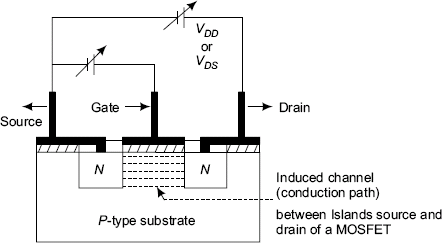
FIGURE 3.39 Induced channel during operation of MOSFET
With enough positive bias voltage, VGS, the electron enhancement will be sufficient to convert the P-region under the gate to an N-type channel. So, the formation of the induced channel connects the source and the drain islands, so that a conduction channel operates the device. Drain to source voltage VDS causes current flow ID due to the flow of induced electrons along the channel from the drain to source. (Induced channel exists only during device operation).
From the transfer characteristic between the parameters VGS and ID of the MOSFET shown in Fig. 3.40, it can be observed that a minimum gate to source voltage VGST or VTH is required to induce mobile electrons and form a channel between the source and the drain to establish current flow between the two N-Type of islands. This minimum voltage VTH is known as the threshold voltage for the MOSFET. The current IDSS is very small and is of the order of a few microamperes that can be known from the device specifications at the specified threshold voltage VTH or VGST. Varying gate to source voltages VGS control the induced mobile electrons into the channel and thus vary the conductance of the induced channel.
The increasing positive voltages on the gate electrode enhance the conduction electrons in the N-type channel and in turn enhance the magnitudes of the drain current ID. So, the device is called as enhancement mode MOSFET or simply E-MOSFET.
For this enhancement MOSFET, as long as the gate-to-source voltage is less than the specified threshold voltage VTH; the MOSFET is normally in the off condition or OFF-state. Once the positive voltage sufficiently exceeds the threshold voltage VTH, N-type channel is induced and the device switches into the conduction or the ON-state. These binary states of switching of the normally off MOSFET device have good number of applications in digital electronic circuits. The additional feature of isolation or insulation of gate from the source and the drain regions provides infinite input impedance for the device, as the gate current is negligibly small.
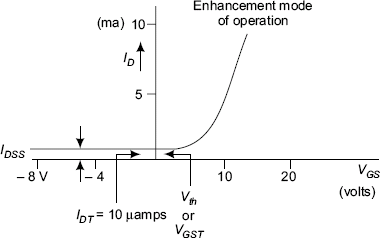
FIGURE 3.40 Transfer characteristic of enhancement mode MOSFET
The device parameters, the drain current ID, VGS and VTH are connected by the following mathematical expression,
where, the value of the constant K depends on the device geometry details. K has the units of mA /(volt)2 and typical value of 0.3 is common.
From this equation for the drain current relating the threshold voltage, it is also clear that the device geometry parameter K has a control on the threshold voltage. In practical digital circuits, the magnitudes of ON voltages depend upon the applications. So, the ON-state voltage of the MOSFET device that is dependent upon the threshold voltage VTH is in turn decided by the design constraints on the MOSFET device to provide a suitable threshold voltage for the desired practical applications.
Output Characteristics for an N-Channel Enhancement Mode MOSFET Output characteristics of MOSFET device are graphs of the drain current ID that will flow as VDS is varied for a number of values of VGS.

FIGURE 3.41 Output characteristics of N-channel E-MOSFET
For an enhancement mode MOSFET, ID = 0 for VGS = 0 volts and hence it almost touches the VDS - axis. The device characteristics are similar to JFET device output characteristics.
As VDS is increased, initially ID increases till knee points on the output characteristics and beyond knee points drain current ID remains almost constant, even if VDS is increased. So, in the constant current regions, the output impedance of the MOSFET device is very high.
Depletion Enhancement MOSFET (DE MOSFET) (MOSFET with Built- in channel) A channel with charges corresponding to majority carriers of source and drain semiconductor materials is diffused between source and drain to form the built-in channel.
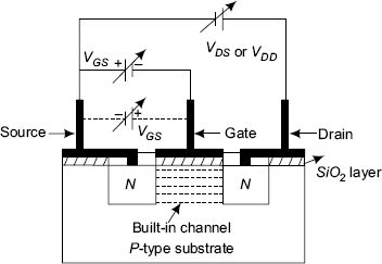
FIGURE 3.42 Structure of an N-channel (built-in channel) depletion enhancement mode MOSFET (DE MOSFET)
DE MOSFET or depletion-mode MOSFET is also known as a normally ON MOSFET, because with zero gate to source voltage VGS, the two N-type islands, the drain and the source are connected by N-channel.
Negative charges or voltage –VGS on the metallised gate induce corresponding positive charges in the N-channel on the other side of SiO2 layer. The induced positive charges may also be thought of as repelling negative charges in the N-channel, with a consequent reduction in the conductivity of N-channel for depletion mode of operation of the device.
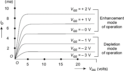
FIGURE 3.43 Output characteristics of DE MOSFET

FIGURE 3.44 Transfer characteristic of N-channel DE MOSFET
In addition to being operated as depletion-mode device, DE MOSFET can also be operated as an enhancement device. Positive gate voltages VGS induce negative charges into the already built-in N-type channel. This enhances the channel conductivity, resulting in more drain current, ID by applying VDS.
The enhancement mode and the depletion mode characteristics of the DE MOSFET are shown in the Fig. 3.43.
3.9 Unijunction transistor
UJT was first introduced in 1948 and is commercially available since 1952.
The unijunction transistor (UJT) or P-N transistor is a two-layer P-N device with three terminals known as emitter, base-1 (B1) and base-2 (B2). Similar to the bipolar junction transistor, the UJT is fabricated on a lightly doped N-type silicon bar with ohmic contacts for the two base terminals B1 and B2 at the top and lower ends of the bar. The emitter section is a heavily doped P-type material that is deposited between the base B1 and base B2 regions, possessing only one P-N junction of small area as shown in the Fig. 3.46. As the device has only a single junction, it is known as a unijunction transistor.
The UJT device exhibits negative resistance characteristics as shown in Fig. 3.49. This means that an increase in emitter current results in a decrease of voltage between the emitter E and base B1 terminals.
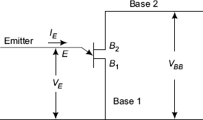
FIGURE 3.45 Unijunction transistor (UJT)
This negative resistance property of the device is made use of in relaxation oscillator circuits used as a time base voltage in cathode ray oscilloscope. It is also used to provide triggering voltages to SCR device control applications and timing circuits.
Emitter arrow shown on the circuit symbol is inclined towards base B1. Pointing in the direction of conventional current (hole) flow when the emitter to base B1 junction of the device is forward biased by the emitter voltage VE.
The main operational difference between FET and UJT is that the gate surface of FET is much larger than the emitter junction of UJT. FET is normally operated with gate junction reverse biased, where useful behaviour of UJT occurs when the emitter is forward biased.
The structural details of UJT are shown in the Fig. 3.46. High resistively N-type silicon (lightly doped / increased resistance characteristic) of 8 × 10 × 35 mils called base B that has attached to its opposite (top and lower) ends two ohmic contacts base B1 and base B2. A 3-mil aluminium wire, called emitter E is alloyed to the base between base B1 and base B2 to form small area of a P-N rectifying junction. Unijunction transistor (UJT) was originally known as doublebase diode. Aluminium rod is alloyed to silicon semiconductor slab closer to base B1 contact as shown in the Fig. 3.46.

FIGURE 3.46 Structural details of unijunction transistor
UJT Circuit with Biasing Voltages
To obtain the UJT device characteristics and understand the working of the device, voltage, VBB is applied between base B1 and base B2. Voltage VEE is used to provide a voltage VE that is applied between the Emitter E and the Base B1 as shown in the Fig. 3.47. Maintaining a constant supply voltage of say 0 volts; varying the emitter voltages in increments, the corresponding value of emitter current IE are noted down. The observations are tabulated. Observations are made for different constant values of VBB = 5 volts, 10 volts, 15 volts and 20 volts. UJT characteristics can be drawn from the tabulated data. During the observations, the salient features such as peak voltage VP, peak current IP, valley voltage VV, valley currents IV, saturation voltage, and so on are noted down, keeping in view of the expected characteristic of the UJT device.
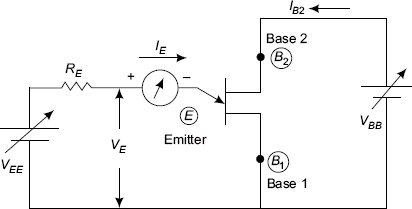
FIGURE 3.47 UJT biasing voltages to obtain UJT characteristics
UJT Equivalent Circuit
Equivalent circuit of the UJT device in the Fig. 3.48 has two resistors RB1 (variable resistance) and RB2 (fixed resistance) that form a voltage divider during the operation of UJT and a single diode representing the P-N junction between the emitter and the base B1. That is the reason why the device is called a unijunction transistor. RB1 may vary from 5 KΩ to 50 Ω for a corresponding change of IE from 0 to 50 milliamperes during the device operation.
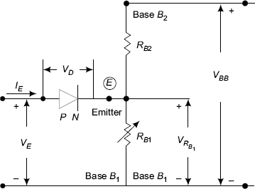
FIGURE 3.48 UJT equivalent circuit for device working
The resistance RB2 is a fixed internal resistance between the emitter and base-B2. The resistance RB1 is the internal variable resistance of the silicon bar between the emitter and base B1 that depends on the operation or ON–OFF states of the UJT device. Inter electrode base resistance RBB = RB1 + RB2 (IE = 0), that is when VE = 0 V. RBB is typically in the range of 5 KΩ to 10 KΩ. The position of aluminium rod functioning as the emitter electrode will determine the relative values of RB1 and RB2 with IE = 0.
Knowing η the intrinsic standoff ratio of the UJT device and the applied voltage VBB across base terminals we can calculate voltage across RB1.
where, η is called intrinsic standoff ratio, the main parameter of the UJT device.
Typical values of η have a range from about 0.5 to 0.8 for most UJTs.
Power dissipation = 300 mw; RMS IE = 50 mA; Peak IE = 2μA
Emitter reverse voltage = 30 V. Inter-base voltage= 35 V.
Principle of Working of the UJT Device
Initially, when VBB is switched on, and the emitter voltage VE = 0 volts; voltage across RB1 will be of such a polarity that will reverse bias the P-N junction between the emitter and base B1. Only reverse current IE0 of the order of a few microamperes will be present through the device in the emitter circuit and the UJT device is in the off-state. The device is in the cut-off region of the characteristic shown in Fig. 3.49

FIGURE 3.49 UJT characteristic
For applied potential, VEE; with increased voltages, when VE is greater than VRB1 = ηVBB by the forward voltage drop across the diode VD, (VD = 0.35 to 0.7 volts, as UJT has silicon semiconductor bar); as shown in the Fig. 3.47 and 3.48; the diode (P-N junction between the emitter and base B1) is forward biased and the UJT will fire. Emitter current IE will begin to flow through RB1 in the emitter circuit due to the heavy injection of majority carrier holes from the emitter into base B1. The emitter firing potential VP is given by VP = ηVBB + VD
UJT characteristics for different values of VBB are shown in the Fig. 3.50.
The UJT characteristics are shown in the Fig. 3.50 for VBB = 5 V; 10 V; 20 V and 30 volts.
For emitter potential to the left of the peak point, the magnitude of IE is never greater than IEo (μA). The current IE0 corresponds very closely to the reverse leakage current IC0 of the conventional bipolar transistor. UJT will be in the off-state during this operation and this region is called the cut-off region as shown in the Fig. 3.49.
Once the voltage VE is greater than or equal to the peak voltage VP; the emitter potential VE will drop with increase in IE. At this stage, the P-N junction between the emitter and base B1 is forward biased. So, the emitter current IE increases. This increase in the emitter current is due to the injection of a good number of majority carrier holes from the P-type emitter region into the semiconductor bar towards base B1. This increase in conduction reduces the resistance RB1 to a very small value, resulting in reduction of VRB1. This forward biases the diode more and the process becomes cumulative resulting in regenerative action. The result is that for increased IE, VEB falls to ultimately reach VV. From the peak voltage VP to VV, the UJT device exhibits negative resistance (after the peak point VP up to the valley point, VV the emitter current IE increases but the emitter voltage VE decreases causing the negative resistance region on the UJT characteristic), which is stable enough to be used in practical circuits such as relaxation oscillator.

FIGURE 3.50 UJT characteristics
Eventually, the valley point VV will be reached and any further increase in IE with increase in VE will place the device in saturation region. In this region the characteristics approach that of semiconductor diode with forward bias.
The decrease in resistance in the active region is due to the holes injected into the N-type slab from the aluminium P-type rod when conduction is established. The increased hole current in the N-type material will result in an increase in the number of free electrons in the slab producing an increase in conductivity G and a corresponding drop in resistance (R ↓ = 1/G ↑).
The three other important parameters of the UJT are IP, VV and IV.
Example—UJT relaxation oscillator
η = 0.55, RBB = 10 KΩ, VV = 2.0 V, VP = 6 Volts, VBB = 10 Volts, IV = 5 mA, IP = 50 μA and RB1 = 200 Ω. During discharge phase resistor R1 should be so chosen as to ensure that load line determined by R1 passes through the characteristics in the negative resistance region to the right of peak and left of valley point.
The voltage across the capacitor C due to charging through RE to the supply voltage VBB while the UJT is in the off-state and discharging through the conducting UJT through RB1 and R1 is according to the following equation and the voltage wave form is as shown in the Fig. 3.52.

FIGURE 3.51 UJT oscillator
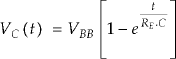
The behaviour of the UJT oscillator circuit as one of the applications of UJT device can be explained as follows. The REC combination across which VBB is connected allows the voltage across the capacitor VC to build up from 0 to the peak voltage VP (VP is as explained on the UJT characteristic) exponentially. When once VP is reached the UJT is triggered to the ON state. This allows the capacitor, which is charged with voltage VP that is VC, has gone up to VP to discharge through RB1 almost instantly since RB1 becomes very low. The device turns off and the process repeats generating a near sawtooth voltage wave form across the capacitor.
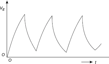
FIGURE 3.52 UJT oscillator output voltage
The output voltages of UJT can be used as trigger voltages to SCR and its other family of devices. In this UJT relaxation oscillator circuit of Fig. 3.51, the resistor R, the capacitor C and the resistances RB1 and RB2 predicted by the intrinsic stand-off ratio η of the device determine the frequency of oscillations of UJT and the output signal frequency according to the following equation.

FIGURE 3.53 UJT device terminals
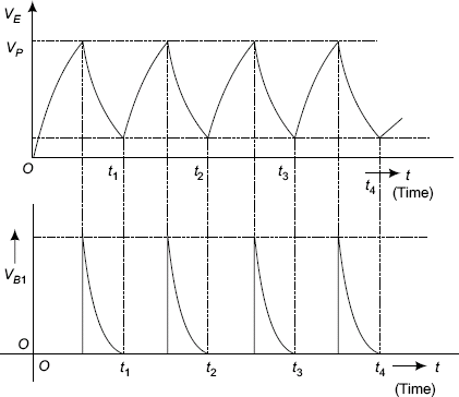
FIGURE 3.54 Wave forms of UJT oscillator

Calculation of range of values of R1 to ensure working of UJT as an oscillator of Fig. 3.51
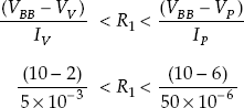
Value of R1 lines between 1.6 KΩ to 80 KΩ R1 is chosen as 68 KΩ in this range.
3.10 Silicon Controlled Rectifier (Thyristor)
SCR devices are used in industrial power control applications, such as powers delivered to electric motors or induction heating elements or relay controls where the power delivered has to be controlled. In high power circuits, variable resistance control elements involve in power dissipations in controlling elements and result in power wastage. Controlled rectifier devices (similar to thyratron devices of vacuum tubes) such as Silicon Controlled Rectifiers (Thyristors) are developed to control large amounts of power using small amount of powers in the gate circuit.
Silicon controlled rectifier is obtained by adding a third P-N junction to the normal transistor structure. The silicon controlled rectifier or SCR (Thyristor) is a silicon P-N-P-N or four-layer diode or four-layer device with three P-N junctions J1; J2 and J3 with three leads attached to the semiconductor materials called anode (A), gate (G) and cathode (K) with its circuit symbol as shown in Fig. 3.55. The gate terminal is added to the cathode of the familiar diode symbol. The diode arrow points in the possible easy-flow direction for current through the SCR. Gate voltages control the conduction of the SCR. The term anode implies that the terminal so named is normally connected to a voltage source in such a manner as to make it positive relative to the cathode for the device functioning.

FIGURE 3.55 Silicon controlled rectifier (SCR) (Thyristor)
Silicon controlled rectifier with four P-N-P-N layers of semiconductors is a four-layer diode with three diodes D1; D2 and D3 (virtual connection) as shown in Fig. 3.56. These diodes with junctions J1; J2 and J3 are considered with the biasing voltages that forward or reverse bias the junctions for understanding the SCR device working depending the anode voltage VAA and gate voltages VGG. The conduction or non-conducting states of SCR are predicted from the applied operating voltages.
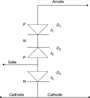
FIGURE 3.56 SCR considered as diodes with junctions (virtual diodes concept)

FIGURE 3.57 Experimental set up for SCR characteristics
Fig. 3.57 shows the basic circuit diagram to obtain the SCR characteristics.
For negative anode-to-cathode voltage VAK, central junction J2 in the Fig. 3.55 is prone to be forward biased, but the outside junctions J1 and J3 are reverse biased. As a result, this is a reverse blocking diode and the characteristic for negative voltage VAK appears as shown in the third quadrant of the Fig. 3.58. The OFF-state resembles that of a reverse biased diode. No reverse current flows unless the avalanche breakdown voltage is exceeded.
For positive VAK, the two junctions J1 and J3 are forward biased and the central junction J2 is reverse biased. For positive VAK, the current at low voltages is limited by the reverse bias behaviour of junction J2 (central junction J2 acts as a dam). Only a small forward leakage current IFX flows through the SCR until the anode is made very much positive relative to the cathode.

FIGURE 3.58 SCR forward and reverse characteristics
As the applied voltage increases, the current increases slowly until the breakover voltage VBO (for the central junction) is reached. At this point, it is interesting that once the dam is broken, so to speak, current floods easily through the device (the current rises abruptly) with only a small voltage drop of one volt (the voltage across SCR drops sharply) across the SCR (from anode to cathode), and the diode has switched to the ON-state. That is, the SCR has changed from an open-switch mode to a mode much like forward biased diode or a closed switch. Before forward breakover the central junction J2 is in the blocking state (due to reverse bias to junction J2) and at the VF(BO)O the central junction J2 breaks under reverse breakdown.
However, when a gate current is supplied to the SCR, the forward breakover voltage (but not the reverse breakdown voltage) is reduced in proportion to the gate current. If a gate current greater than some gate-trigger current IGT is supplied to the gate, the device goes into the break over or conduction state for a small positive anode-cathode voltage of the order of 1 to 2 V. The gate must be positive by only about one volt relative to cathode to cause the gate make trigger current IGT to flow. This voltage forward biases the bottom P-N junction. For low power SCRs IGT < 0.1 mA and for high power SCRs IGT > 15 mA, although some minimum is required in some cases.

FIGURE 3.59 SCR firing characteristics
The voltage for reverse breakdown is about the same as the SCR’s forward breakover voltage (for IG = 0). As was true for normal diodes, the reverse breakdown situation can ruin by overheating the diode, if the current is allowed to become large. The SCR is not ruined in the forward direction breakover case since VAK, the anode-cathode voltage quickly drops to about one volt and the device is designed to carry that current, (the V.I product is then very small) as shown in the SCR characteristics in the Fig. 3.59. Typical SCRs can pass a current of 1 to 15 amperes in the forward direction without harm, depending on the SCR rating and with proper heat sinking.
SCR Concept as Two Back-to-Back Connected Transistors
The switching operation of the four-layer device, the SCR can be understood as two interconnected transistors. In Fig. 3.60, SCR device is considered as a back-to-back combination of P-N-P and N-P-N transistors that are shown physically displaced but electrically connected. The two transistors have a common collector junction.

FIGURE 3.60 Two-back to back connected transistors concept
From the Fig. 3.61, observing the flow of currents through the two transistors T1 and T2, it can be seen that IA = IE1 = IE2 and IA = (IC1 + IC2), where IC1 and IC2 are as following.
From Fig. 3.61, the collector currents will be obtained by summing the currents into the Transistor T1. Substituting the values of IC1 and IC2 in the equation IA – IC1 – IC2 = 0.
IA − α1IA − IC01 − α2.IA − IC02 = 0 using IA = IC1 + IC2
∴ IA [1 − (α1 + α2)] = IC0 where IC0 = IC01 + IC02 (3.38)
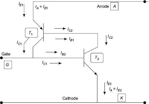
FIGURE 3.61 SCR shown as interconnected transistors
Current gain of a transistor varies with collector current. So, at low currents α is small. As, IA increases with an increase in VAK, α1 and α2 increase. As the quantity (α1 + α2) approaches unity, current tends to increase without limit and breakover occurs. After switching ON the voltage across SCR is smaller than one volt and only the resistance in the external circuit limits the current.
Once in the conduction state, the SCR remains so even after the gate current/voltage is removed. The SCR remains in the ON-state until the anode voltage is reduced so that the anode current falls below a small holding current IH (typically a few mA). The SCR will be certainly turned off if the anode is actually made negative relative to the cathode. However, a negative voltage to the SCR gate will not turn off the SCR. The turn-on time for a SCR is of the order of 1 μ sec, while the turn-off time after reverse bias is about 20 microseconds.
The introduction of gate current of the order of a few microamperes switches the SCR (Thyristor) to the ON-state at voltages lower than VBO for the corresponding diode. Such a silicon controlled rectifier provides flexible switching and since the gate current is required only momentarily very efficient control of large currents in the anode circuit can be achieved with virtually a few microamperes of gate current that too momentarily. Therefore, the firing voltage is a function of gate current IG. In comparison to power transistors, SCRs (Thyristors) are designed with thick base layers for high voltage capability and necessary low α characteristic. Currents may be larger because the total junction areas are available for conduction.
The characteristics of SCR are shown in the Fig. 3.62.
As can be observed from the forward characteristic of Fig. 3.62 of the SCR device, during the positive voltages of VAK from zero to the forward breakover voltage VBO, the device functions as an open switch because of the central P-N junction J2 being under reverse bias and not allowing the current flow as a dam, even if the outer junctions J1 and J2 are under forward biased situation. During this region the anode current is of the order of a few microamperes and hence SCR behaves as an open switch with a very high resistance of the order of megaohms, the SCR being in the off-state or no conduction state. Once the anode voltage reaches the forward breakover voltage VB0; the dam effect of central junction J2 is broken resulting in flooding of anode current through the device. Now, the device is in the ON-state or conducting state and acts as a closed switch and at the same time, the voltage across SCR drops down to the saturation voltage of about one volt, with a consequent decrease of power dissipation across the device, as the product of the anode current and the saturation voltage across SCR is of the order of few watts. This does not cause any damage to the device. That is one of the main reasons for controlling large amounts of power.

FIGURE 3.62 SCR firing characteristic
Firing Voltage It is defined as the minimum voltage, which is required between anode and cathode of a Thyristor (SCR) to trigger into conduction. Firing voltage is slightly more than ON-state voltage. (Firing voltage is a function of gate current IG as shown in Fig. 3.63).

FIGURE 3.63 SCR characteristics for different gate currents
Latching Current (IL) It is the minimum current required to latch the device from OFF state to ON state. It can also be said to be the minimum current required to trigger the device. Typical values of latching current may range from 8 mA to 10 mA.
Holding Current (IH) It is defined as the minimum current required for holding the device in conduction. Below this value of current the device cannot conduct and the device returns to the OFF-state. The typical values of holding current of a device may range from 3 mA to 5 mA.
Gate Current (IG) It is the current, which flows into the gate terminal to control the stage of device conduction.
Turn-on Time Though the Thyristor is a very fast switching device, it does not switch instantly, rather it takes finite time to reach its full conduction from the time the trigger signal is applied. In other words, it is called response time, also. The typical values of TON range from 150 nanoseconds to 200 nanoseconds.
Turn-off Time A reverse voltage has to be applied across the device to turn-off from conduction state of the device. It takes a finite time after application of reverse voltage to switch the device OFF (commuted). This time is called the turn-OFF time of the device. The typical values of turn-off time are 200 nanoseconds.
Ratings Peak inverse voltage (VPIV): It is defined as the maximum voltage, which the device can safely withstand in the OFF-condition. VPIV depends on temperature and ON-state voltage. The voltage drop across the Thyristor when conducting is very low. This voltage is called the ON-state voltage of Thyristor. The typical value of this voltage lies between 1volt to 4 volts.
Questions for Practice
- Indicate the different current components of a collector current IC of a bipolar junction transistor (BJT) and substantiate the name BJT given to a transistor.
- Draw a circuit diagram to illustrate the methods of biasing a BJT for the transistor to act as an amplifying device.
- For a transistor biased to operate in the active region of the device characteristics, in spite of the fact that the collector junction is reverse biased, collector current IC is large. Predict the reason.
- A transistor connected in CE configuration is biased to operate in active region of the device characteristics when Vce = 12 volts, IC = 10 mA and Ib = 50 μA. Calculate the value of beta (β) of the transistor.
- Mention the influence of early effect on output characteristics of a common emitter operated transistor.
- Discuss the significance of maximum allowed power dissipation at the collector junction of the transistor.
- Show the various operating regions on the output characteristics.of a CE transistor.
- Predict the region of operation on the output characteristics of a common emitter operated transistor so that the transistor is to be used as a linear amplifier.
- Illustrate the influence of early effect on the output characteristics of a common base operated transistor.
- For a transistor operated in CB configuration; IC = 5.2 mA and Ie = 5.5 mA. Calculate the value of alpha (α) of CB transistor. Also, calculate Ib.
- Mention the reason why the output resistance of CE transistor biased to act, as an amplifying device is low.
- Draw the small signal low frequency equivalent circuit of a transistor.
- Define the h-parameters of the transistor in CE Configuration.
- What is the reason for calling the transistor h-parameters as hybrid parameters?
- For a T-network having in each arm of a resistance of value 100 ohms, calculate h11.
- From the definition of β of a transistor derive the relation between β and α of a transistor.
- From the definition of α of a transistor derive the relation between β and α of a transistor.
- For the transistor to act as a switch mention the nature of biasing voltages for input and output junctions of a transistor.
- Mention the relation between the components IC, ICo and a of a transistor.
- Change of Ic with VCB in active region is due to _____ and IE components of a transistor.
- Justify the reasons for the transistor to behave as a current controlled current source.
- Mention the relation between ID; IDD; VGS and Vp of a Field Effect Transistor.
- Mention the main advantages of JFET over BJT.
- Mention the reason for high input resistance of JFET.
- Justify the reasons for JFET to function as voltage controlled voltage source.
- Draw the equivalent circuit of JFET device.
- Indicate pinch-off voltage on the JFET output characteristics.
- Mention the various operating regions on output characteristics of JFET device.
- Define drain saturation current IDSS.
- The disadvantage of a JFET is its _____ voltage gain.
- Find the value of VGS to make ID = 12 mA, given IDSS = 15 mA and Vp = 5 volts.
- CC transistor with a load resistance RL in the emitter has a _____ input resistance.
- For a JFET device, IDSS = 8 mA and pinch-off voltage Vp = −4 volts. Predict the value of VGS for class A operation of the device and calculate the value of drain current ID.
- Define the JFET device parameters and establish the relation between them.
- Mention the maximum voltage gain that can be realised from a JFET device.
- JFET device has a main advantage over BJT device (a) high input impedance (b) higher gain-bandwidth (c) low noise (d) large gain.
- Mention the reason for calling the MOSFET with induced channel as normally off MOSFET.
- Explain the concept of how a enhancement MOSFET device functions as a switch.
- Mention whether E-MOSFET or DE MOSFET has built-in channel in the device.
- Mention the main advantage of DE MOSFET over E-MOSFET.
- Explain the two types of concepts of pinch-off voltage for a JFET device.
- Explain the reasons for varying depletion region widths in a JFET device during the operation of the device.
- Explain the concept of threshold voltage for the working of a E-MOSFET device.
- Mention the expression relating the threshold voltage VTH and the other parameters of the device E-MOSFET.
- Substantiate the reasons for the use of JFET at the input stages of electronic instruments.
- Draw the structure diagram of N-channel JFET device.
- Draw the structure diagram of P-channel JFET device.
- Mention the biasing voltages on a circuit diagram to obtain the JFET characteristics.
- Draw a typical transfer characteristic of JFET device with IDSS = 10 mA and VP = −4 volts.
- Determine the transconductance gm of a JFET device with the drain saturation current IDSS = 10 mA and VP = −4 volts at constant drain to source voltage VDS = 10 volts.
- Define the pinch voltage VP with reference to the transfer characteristic of JFET device.
- Define drain saturation current IDSS from the JFET characteristics.
- Define drain resistance rd and of a JFET and determine the value of rd if ∆VDS = 10 volts and ∆ID = 0.2 mA when VGS = −2 volts (constant).
- Define amplification factor μ of a JFET device and derive the relation between the three device constants μ, gm and rd.
- If the amplification factor μ of a JFET device is 25, mention the maximum value of voltage gain that can be realised from an ideal JFET amplifier.
- Define breakover voltage of a silicon controlled rectifier.
- Define holding current of a silicon controlled rectifier.
- What is the minimum voltage required to keep the UJT device in the ON-state?
- In which region a bipolar junction transistor can act as a switch?
- Explain about basewidth modulation phenomenon in a transistor.
- Explain the functions of junction capacitances in a transistor.
- Derive the relation between α and β parameters of CB and CE operated transistors.
- Explain thermal run away phenomenon in transistors and how they are taken care of in the device operations.
- Discuss the differences and common features of N-P-N and P-N-P transistors.
- Define the transistor h-parameters in cB Configuration.
- Define stability factor and explain its significance in transistor biasing circuit design.
- Mention the method of finding whether a transistor is in its active region or not.
- Discuss the conditions and the reasons for using heat sinks with transistor devices.
- Can we call the stability factor as instability factor based on the real time situations of transistor to be operated in stable conditions Substantiate the answer.
- Write a condition to avoid thermal runaway in transistors during their practical operation.
- Discuss the method of determination of gm for a transistor.
- A certain JFET has IDSS = 36 mA at VGS = 0 volts. VGS is equal to half the pinch-off voltage VP, calculate the magnitude of drain current ID.
- Calculate the magnitude of input resistance of the JFET, when the gate current IGS = 10 μA for an applied voltage VGS = 2 volts.
- For a FET device gmo = 2500 × 10−6 Siemens, calculate the value of transconductance gm when the device operating voltage between the gate and the source VGS has a design value of half the pinch-off voltage, when the FET device is used in an amplifier circuit.
Points to Remember
- For a JFET device, the drain current ID = IDSS when VGS = 0 volts from Shockley’s equation. This maximum drain current when VGS = 0 volts is known as drain saturation current IDSS. This can be observed on both the output and Transfer characteristics of the FET device.
- The value of drain to source voltage at which the channel is pinched-off is known as pinch-off voltage VP.
- A JFET device is a unipolar device because the device current, the drain current is due to the flow of majority carriers only.
- A FET device has small gain-bandwidth product.
- A JFET device is a voltage controlled voltage source.
- For small voltages of VDS, the drain to source voltage, the FET behaves as a simple and linear resistor.
- JFET has three device parameters μ, gm and rd and are related by μ = gm.rd.
- The Shockley equation for JFET device is
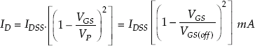
- A JFET behaves like a variable resistor in the ohmic region of output characteristics and as a constant current source in the pinch-off region.
- A JFET has high input impedance and low output impedance and as such, used at the input stages of electronic instruments.
- A MOSFET is used in digital electronic circuits, because it can be operated as a binary switch.
- DE MOSFET can be operated with both types of polarity voltages to gate voltages.
- MOSFET device is also known as insulated gate FET (IGFET).
- A JFET is a square law device and hence can be useful as a tuner in radio and TV circuits.
- The conducting region in FET devices is called as a channel.
- The main disadvantage of a JFET device is its low voltage and is limited theoretically to a maximum value μ, the amplification factor of the device.
- Since, JFET has no off set voltage, the device has an application in chopper circuits.
- The input resistance of a JFET device is very high, since the gate junction of the device is reverse biased and the input gate current is almost negligible or zero.
- JFET operated in the ohmic region of the output characteristics can be used as a Voltage Variable Resistor (VVR).
- Silicon transistors operate at high temperatures because of the silicon semiconductor has a wide forbidden band-gap energy.
- The collector area is larger in transistor devices to allow for much heat dissipation.
- The N-P-N transistors are preferred over P-N-P transistors, because of the high mobility μ of the electrons during conduction with resulting good frequency response of N-P-N transistor amplifiers.
- BJT is a bipolar device because, the currents in the device are due to the movement of both electrons and holes in the transistor device.
- For a good transistor it is necessary that all the injected electrons from the emitter to the base region (for N-P-N transistor) have to reach the collector so that the two currents IE and IC are almost equal. To achieve this, the base region of the transistor is made of small area of cross-section for the electrons to spend less time during their journey to the collector and further, the base region is lightly doped to minimize the numbers of recombination of holes in the P-material with electrons in the transit
- A transistor has two P-N junctions, one between the emitter and base regions known as the emitter junction or the input junction and a second P-N junction between the base and collector regions known as the output junction or the collector junction.
- Bipolar junction transistor can be treated as two diodes connected back to back for understanding the operation of the device as concept of P-N junctions is mostly useful for the working of semiconductor devices.
- The transistor is a current controlled current source.
- The main difference between JFET and BJT is that the input junction of the gate of FET device is reverse biased and has very large input resistance, whereas the input junction of the BJT is forward biased and hence the input resistance of transistor is very low.
- The transistor is operated as a linear amplifier when the D.C. operating conditions of the transistor are fixed in the active region of the output characteristics of the device.
- The transistor operating voltages are fixed in the saturation and the cut-off regions for the transistor to operate as an electronic switch.
- The type of semiconductor material can be determined using Hall effect.
- Effect of basewidth modulation is more pronounced on the output characteristics of a common emitter operated transistor over a common base operated transistor, because of the large value of current gain β of CE transistor when compared to a very low value of current gain α of a common base transistor.
- The emitter junction of the transistor is forward biased and its collector junction is reverse biased for the transistor to act as an amplifying device.
- The reason for the very low input resistance of a transistor is the forward bias to the input junction of the transistor and its consequent low resistance.
- The negative resistance region lies between the peak and valley points of emitter voltages on the UJT characteristics.
- There are two positive regions on the UJT characteristics before the peak point and after the valley points of emitter voltages on the UJT characteristics.
- The intrinsic stand-off ratio of a UJT device lies between 0.5 to 0.8.
- UJT device can be used in negative resistance oscillator circuits when its operation is in the negative resistance region of the device characteristics.
- UJT output across the capacitor finds its use as a sweep voltage in CROs.
- The UJT output voltage can be used as a triggering voltage in SCR circuits.
- A UJT device comes into conduction state when the emitter voltage VE is equal to the peak voltage VP on the UJT characteristics.
- A common emitter operated transistor configuration is more popular because of its large values of voltage and current gains.
- In a transistor the emitter region is more doped than the collector and the base regions.
- The E-MOSFET operates with enhance mode only for the induction of the channel between the drain and source islands in the device for the device to come into the conduction or ON-state, otherwise E-MOSFET is initially in the normally OFF-state.
- There is no thermal run away phenomenon in the FET devices as the input signal voltages to the FET device are of the order of volts and the voltage equivalent of temperature VT is of the order of 26 mv at 300°K, which tries to perturb the input signal operations has negligible contribution.
- The JFET device operates only in depletion mode.
- The electron mobility is larger when compared to hole mobility in the solid semiconductor medium, because of the small mass for the electrons. So, the N-channel MOSFET devices work faster than P-channel MOSFET devices.
- The input impedance of the MOSFET (IGFET) device is high because of the insulating layer SiO2, between the gate and the conducting channel of the device.
- The N-channel MOSFET device is normally off when VGS = 0 volts.
- The gate-to-source voltage that turns on the E-MOSFET device is called as threshold voltage and it also depend upon the geometry of the device as the constant K connecting the drain current is ID = K. (VGS − VTH)2.
- The DE MOSFET works either in enhancement mode or depletion mode depending upon the practical applications.
- ID = K(VGS − VTH)2 for enhancement-MOSFET device transfer characteristic.
- In a DE MOSFET device, the method of reducing the conductivity of the channel between drain and source of the device by applying suitable polarity voltage at the gate terminal for removing or depleting of the free charges in the channel is known as depletion operation.
- The enhancement MOSFET has no physical or built-in channel. The device works on the induction of channel between the drain and the source on applying suitable polarity voltage at the gate electrode.
- Reverse biasing voltages at the P-N junctions of the FET device produce depletion region widths in the channel, thereby increasing the channel resistance.
- Enhancement MOSFET requires a minimum gate-source voltage VGS for induction of channel between the drain and the source for device conduction. So, E-MOSFET will not work for zero voltage of VGS. So, E-MOSFET has no IDSS parameter.
- DE MOSFET has a physical or built-in channel for the device working.
- The difference between JFET and MOSFET is that JFET has a PN-junction.
- The constant current area on the drain characteristics of FET device occurs in the pinch-off region or the region between the pinch-off voltages Vp to the point of just nearing the breakdown point.
- The gate-source voltage on the N-channel JFET device should either be zero or negative so as to maintain the very high input resistance of the device by maintaining the reverse biasing voltages at the gate-source junctions.
- The depletion region widths close the channel completely (but never overlap) when the drain current is zero at the pinch-off voltage or VGS (off) for the FET device.
- The channel of a JFET is between the drain and the source.
- MOSFET has insulated gate electrode from the drain and the source.
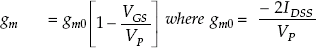

- The negative resistance region of UJT characteristic is used in the design of relaxation oscillators using UJT devices.
- For a transistor to be operated as an electronic switch, the D.C. operating conditions are fixed in the cut-off and saturation regions.
- The values current gain β of CE transistor change from one transistor to another transistor of the same type and so the stability of operation gets effected whenever a transistor is replaced with another unit of the same make and device number.
- Transistors are classified generally as low or medium power transistors, power transistors, switching transistors, low frequency transistors and high frequency transistors depending on their applications in the practical circuits.
- Making use of the property of a P-N junction with reverse bias voltage has large value of reverse resistance Rr and the P-N junction with forward bias will have a very low value of forward resistance Rf, a bipolar junction transistor can be tested with a multimeter for its failure or not keeping in view of the behaviour of the transistor device having two P-N junctions one at the emitter-to-base junction and the second PN-junction at base and collector areas of the transistor.
- Explanation of why the current gain α for CB transistor is less than 1. The current gain alpha α of the transistor is defined for common base operated transistor.

From the definition of the current gain alpha, the output current, the collector current IC is less than the input current, the emitter current IE. Hence, the current gain α < 1. Further, the emitter current (IE) and the collector current (IC) are approximately equal. So, alpha is approximately unity.
- Explanation of why the current gain β for CE transistor is >> 1. The current gain beta β of the transistor is defined for common emitter operated transistor.

From the definition of the current gain beta, the output current; the collector current IC is very much greater than the input current, the base current IB. Hence, the current gain β >> 1.
- Explanation of how the transistor is considered as current controlled device.
The transistor operates in the active region when the base-emitter junction J1 is forward biased and the base-collector junction J2 is reverse biased irrespective of the transistor configuration. Emitter region is heavily doped and so large numbers of electrons are injected from the emitter into the base region. That is how the emitter is considered as the source of electrons. The emitter current IE is the sum of majority carrier electron current and the minority carrier hole current in the N-P-N transistor.
All the electrons that cross the emitter-base junction do not reach the collector, since there are some recombinations with holes in the base region contributing to very small magnitude of the base current IB and the remainder enters the collector and the collector current component is INC. There is a small minority carrier current due to reverse bias of the base-collector junction designated as the current IC0.
The net collector current will be IC = (IC0 – INC); if IE is not equal to zero. When IE = 0, the collector current IC = IC0; since INC representing the injected carrier current is zero since IE = 0.

The above discussions indicate that the transistor is a current controlled device.
- Diagram showing the biasing circuit for PNP transistor in common emitter configuration. PNP transistor in common emitter configuration with biasing voltages, the forward bias VBE to forward bias the emitter junction and the reverse bias VCE to reverse bias the collector junction (necessary biasing voltages for the transistor to act as an amplifying device) are shown in the Fig. 1.

FIGURE 1 Common emitter (P-N-P) transistor with biasing voltages to obtain input and output characteristics
- Explanation of operation of CE mode P-N-P transistor using its input and output characteristics.
When the input junction is forward biased by VBE, the majority carrier holes are injected from the P-material emitter into the N-material base, overcoming the cut-in voltage of the input junction, (cut-in voltage is seen on the transistor input characteristics in Fig. 2) as majority carriers contribute to the current through the emitter junction. The injected minority carrier holes move by diffusion from the emitter junction to the collector junction. During this journey some electrons of thin and lightly doped N-material base recombine with the diffusing holes contributing to the base current, IB. As most of the emitter current has to reach to the collector to function as a good transistor as the output collector current IC, the recombinations in the base are made deliberately less by light doping and of smaller area of cross-section of the base.
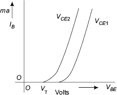
FIGURE 2 Input characteristic of CE Transistor
As the collector junction is reverse biased by VCE the holes, the minority carriers in the base move into the collector region contributing to the collector current. Thus, the emitter current is equal to the sum of the base current and the collector currents. On the output characteristics shown in the Fig. 3, a slight upward slope of the collector current is seen which is due to the early effect due to the reverse bias to the output junction. The output characteristics are drawn for different constant values of the base currents as shown on the output characteristics. Further, the output characteristics find three region of operations, 1) saturation region 2) cut-off region and 3) active region. For the transistor to be operated as an amplifier, the biasing voltages known as the D.C. operating conditions are fixed in the active region of the characteristics for the amplifier to function as a linear amplifier.
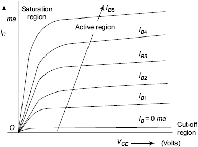
FIGURE 3 P-N-P transistor common emitter characteristics
- The three FET device constants are transconductance gm, drain resistance rd and the amplification factor μ. The following are the definitions with the relation between them:
Transconductance,

Drain resistance,
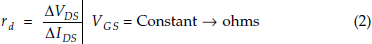
Amplification factor

From these definitions

- Explanation of the operation of the transistor when the emitter junction is forward biased and the collector junction is reverse biased.

FIGURE 1 Common emitter transistor circuit to explain the operation of the transistor as an amplifying device
For a transistor to function as an amplifying device the input junction called as the emitter junction J1 of the transistor is to be forward biased (D.C. source used for this purpose is known as bias voltage) by a voltage and the output junction, the collector junction J2 is to be reverse biased by a voltage. Consider common emitter operated transistor with forward bias VBE to the input junction J1 for the input diode between base and emitter and reverse bias VCE to the output junction J2 for the output diode between base and the collector of the N-P-N transistor as shown in the Figures 1 and 2.
When the forward bias VBE is increased, there are two forces that act on the majority carrier electrons in the N-material emitter of the N-P-N transistor. Force FVBE = e.VBE due to the forward bias pushes the electrons towards the junction, thereby reducing the depletion region about the input diode junction J1 (of the input diode) between base and emitter regions of the transistor. The negative immobile ion charge at the junction J1 in the P-material base region due to the contact voltage (or built-in voltage or barrier potential VB) V0 tries to restrain the entry of electrons with a force FV = eVV0 as long as the barrier potential V0 is not reduced. Once the forward bias VBE overcomes the opposing affect of contact potential, that is, when the actual junction potential (V0 − VBE) at that instant is less than the barrier potential V0; electrons are injected from the emitter into the P-material base region of the transistor.
The movement of the injected minority carrier electrons from the emitter into the base region to the other end of the base area is by diffusion, because of the charge gradient among the injected electrons and the small quantity of originally existing minority carrier electrons in the P-type base material. During this course of journey some electrons recombine with the holes in the base material. These recombinations are less in number, because of the small area of cross-section of the base material and light doping; the numbers of available holes for recombinations are less (for a good N-P-N transistor, almost all the electrons injected from the emitter into the base will be collected and IC is preferable to be almost equal to IE. Hence, the P-type base region should be narrow and the electron lifetime should be long). The lost holes in recombinations are supplemented by positive of VBE contributing to the very small magnitude of the base current IB; which is shown as entering into the base of the transistor. Once the injected electrons are at the junction J2 of the output diode, the electrons enter the collector region because of the reverse bias to the output junction J2 (of the output diode) and then are pulled onto the positive of the supply voltage VCE. So, the collector current IC is into the collector terminal (direction of the conventional collector current IC is opposite in direction to the movement of electrons out of the collector terminal). Also, it can be seen from the directions of flow of the base current and the collector current through the emitter terminal as the emitter current IE; which is the sum of the base current and the collector current.
Mathematically, |IE| = |IB + IC|
Thus, mathematically, IE is expressed as above, for the N-P-N transistor under discussion.

FIGURE 2 CE Transistor with biasing voltages to explain the operation of the transistor
- Explanation of the need for biasing of transistor devices.
Basically, the bipolar junction transistor (BJT) is used as a two-port network or as a four terminal network and functions as an amplifying device along with other applications. The name for the device itself is an acronym formed from the two words transfer and resistor. For achieving different levels of resistance, say, low resistance at the input port, the input junction of the transistor is to be forward biased and to achieve larger resistance at the output port of the transistor output junction is to be reverse biased. These different levels of resistances at the input and output ports of the transistor contribute to the amplifying action of the transistor. Thus, for the transistor to act as an amplifying device, there is need for biasing the input (emitter junction) and output (collector junction) junctions of the transistor.
Further, the quiescent operating point or the D.C. operating point Q of the transistor is located on the D.C. load line drawn on the output characteristics of the transistor, depending upon the class of operation of the amplifier. For linear operation of the amplifier, the quiescent operating point is located at the middle of the D.C. load line for the device operation to be in the active region of the output characteristics and symmetrical input and output voltages. Fixation of the quiescent operating point Q; that is, the quiescent collector current ICQ and the voltage between the collector and the emitter VCE.Q of the transistor are fixed by the biasing voltages for the emitter junction and the collector junctions of the transistor.
- UJT Symbol and reason for the device name as, unijunction transistor
The unijunction transistor (UJT) or P-N transistor is a two-layer P-N device with three terminals known as emitter, base-1 (B1) and base-2 (B2). Similar to the bipolar junction transistor, the UJT is fabricated on a lightly doped N-type silicon bar with ohmic contacts for the two base terminals B1 and B2 at the top and lower ends of the bar. The emitter section is a heavily doped P-type material that is deposited between the base B1 and base B2 regions, possessing only one P-N junction of small area. As the device has only a single junction, it is known as a unijunction transistor.

FIGURE 1 Unijunction transistor (UJT)
- Equivalent circuit of the UJT device in the Fig. 2.
The equivalent circuit of UJT has two resistors RB1 (variable resistance) and RB2 (fixed resistance) that form a voltage divider during the operation of UJT and a single diode representing the P-N junction between the emitter and the base B1. That is the reason why the device is called a unijunction transistor. RB1 may vary from 5 KΩ to 50 KΩ for a corresponding change of IE from 0 to 50 milliamperes during the device operation.
The resistance RB2 is a fixed internal resistance between the emitter and base-B2. The resistance RB1 is the internal variable resistance of the silicon bar between the emitter and base B1 that depends on the operation or ON−OFF states of the UJT device. Inter electrode base resistance RBB = RB1 + RB2 (IE = 0), that is when VE = 0 V. RBB is typically in the range of 5 KΩ to 10 KΩ. The position of Al rod functioning as the emitter electrode will determine the relative values of RB1 and RB2 with IE = 0.
Simplified equivalent circuit for UJT
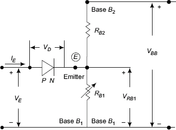
FIGURE 2 UJT equivalent circuit for device working
- UJT emitter characteristics and various regions marked on the Fig. 1
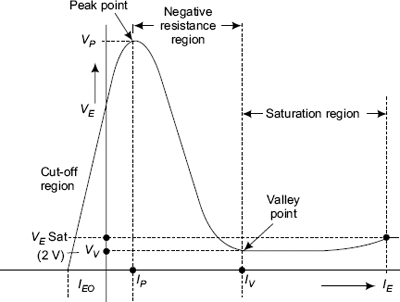
FIGURE 1 UJT characteristic
- Working of UJT device when the emitter voltage VE < VPeak
Initially, when VBB is switched on, and the emitter voltage VE = 0 volts; voltage across RB1 will be of such a polarity that will reverse bias the P-N junction between the emitter and base B1 as can be understood from the equivalent circuit of UJT in Fig. 2. Only reverse current IE0 of the order of a few microamperes will be present through the device in the emitter circuit and the UJT device is in the off-state. The device is in the cut-off region of the characteristic as shown in the Fig. 3 showing the emitter characteristic and the operating regions of UJT device.
Working of UJT device when the emitter voltage VE > VPeak
For applied potential, VBB; with increased voltages, when VE is greater than VRB1 = ηVBB by the forward voltage drop across the diode VD, (VD = 0.35 to 0.7 volts, as UJT has silicon semiconductor bar); the diode (P-N junction between the emitter and base B1) is forward biased and the UJT will fire. Emitter current IE will begin to flow through RB1 in the emitter circuit due to the heavy injection of majority carrier holes from the emitter into base B1. The emitter firing potential VP is given by VP = ηVBB + VD.
- Calculation of the peak voltage Vp
Data η = 0.8 VBB = 15 volts and VD = 0.7 voltsPeak voltage = VP = η.VBB + VD = 0.8 × 15 + 0.7 = 12.7 volts.
- Discussion of the method of determination the quiescent drain current IDQ and the voltage between the drain and the source for JFET from its static characteristics.
Basic JFET amplifier circuit Fig. 1.
Amplifiers consider the input and output A.C. signals for amplification.
Now, consider the JFET amplifier a small signal amplifier as in Fig. 1.
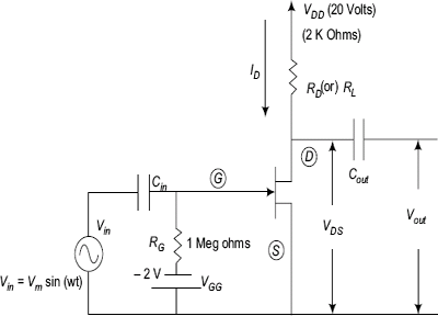
FIGURE 1 Basic JFET amplifier circuit
In the basic amplifier circuit shown in the Fig. 1, both the D.C. voltages are 1) gate supply voltage or gate to source bias voltage VGG used to set the D.C. voltage VGS (based on the type of the amplifier and its class of operation) and 2) drain supply voltage VDD so as to set the drain current (output current) ID flowing through the FET device to a value such that the voltage across the load resistance RL = ID.RL = VRL is about half the supply voltage VDD to satisfy the class A operation of the amplifier.
The bias (D.C. voltage) VGG is arranged such that the gate of the N-channel FET is made negative relative to the source, because the requirement is that gate-channel diode junction of the N-channel FET is to be reverse biased so that the input resistance Rin of the FET device is very large, which is an advantage over the BJT devices and facilitates non-ideal driving voltage amplifiers.
The gate-source voltage VGS is established by the bias voltage VGG as shown in the basic amplifier circuit of Fig. 2. Because there may be a gate current of only of the order of a few nanoamperes, the voltage across the gate resistor RG (10 × 10−9 × 1 × 10 −6 = 10−3 volt) negligibly small and the gate -source voltage VGS is virtually the same as −2 volts. for class A operation of the amplifier. VGS = (1/2). VP.
The swings of the input signal voltage VIN and the output voltage VOUT of the JFET amplifier depend on the location of the quiescent operating point and in turn, on the class of operation of the amplifier depending on the practical applications.
Assume the following output characteristics (static characteristics) for the JFET device as shown in the Fig. 2.

FIGURE 2 Static characteristics of JFET device with DC load line to obtain quiescent voltage and current at quiescent operating point ‘Q’
The output characteristics of the device can be obtained experimentally or by a curve tracer using a cathode ray oscilloscope. When the JFET device is biased with voltages for the required class of operation of the amplifier, steady state values of the drain current ID and the voltage VDS are related by D.C. load line equation for the amplifier analysis.
Obtaining the D.C. equivalent circuit of the amplifier circuit in Fig. 2, the D.C. load line equation can be written as the following:
VDD = VDS + ID.RL……D.C. load line equation.At the point X of the D.C. load line in the Fig. 2; VDS = 0 volts; and the other coordinate is obtained by substituting VDS = 0 in the above D.C. load line equation. Therefore, ID = (VDD/RL). Similarly, for the coordinates of the point Y of the D.C. load line in the Fig. 2, ID = 0 mA, and the other coordinate is obtained by substituting ID = 0 in the D.C. load line equation. Therefore, the other coordinate of point Y is VDS = VDD.
The coordinates of the point (X) of the D.C. load line are VDS = 0 volts and ID = (VDD/RL) and the coordinates of the point (Y) of the line are VDS =VDD volts and ID = 0 mA. Joing the two points, the D.C. load line can be drawn on the static characteristics of the JFET device. The drain current ID.Q and the voltage VDS.Q between the drain and the source of the JFET device corresponding to the selected quiescent operating point are obtained by superimposing the D.C. load line on the static or output characteristics for the required quiescent point operation of the amplifier.
- Explanation of the JFET device as a switch.
As shown in the Fig. 1 the FET device can be used as a switch. The drain supply voltage VDD is applied between the upper end of the drain circuit resistance RD and the ground terminal, with the polarities of the supply voltage suitably oriented depending on whether the FET device is an N-channel FET or a P-channel FET device. The voltage VGS between the gate and source is used to apply suitable voltage to the FET device for turning the device to the ON-OFF states.
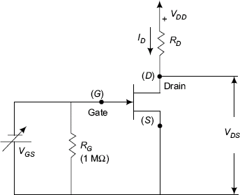
FIGURE 1 FET operation as a switch
Apply drain supply voltage VDD, for example, 10 volts. Apply VGS = 0 volts. The drain current ID will be equal to the drain saturation current IDSS. Then, the voltage between the drain and source VDS is designed to be approximately zero by suitable design value of the drain circuit resistance using the following equation and selecting the FET device that is specially designed to function as a switch with very low value of the ON resistance rdS.
VDS = VDD − ID.RD (1)Now, the effective drain-to-source resistance rDS may be an effective short circuit or a few tens of ohms of the order of 50 ohms.

From the transfer characteristic of the FET device, the drain current ID will be zero at the pinch-off voltage VP. So, as to bring the FET device into the non-conduction state with zero drain current the voltage VGS of magnitude greater than the specified pinch-off voltage for the selected FET device is applied. Then, the voltage across the drain and source VDS of the FET device will be almost equal to the supply voltage VDD, as the resistance between the drain and the source rDS will be so high of the order of mega ohms, that FET can be considered as an open circuit.

The resistances of the FET devices under these two operating situations are known as ON resistance and OFF resistance of the FET device. The ON and OFF states of operation of the FET device suggest the practical use of the device as a switch.
- Verify that collector current of a common emitter mode transistor operated in the active region of its output characteristics is given by the following equation.
When a transistor in common emitter configuration has the emitter junction forward biased and the collector junction reverse biased, the transistor operates in the active region of its output characteristics. Then, the collector current IC is expressed as in the following equation:
IC = β.IB + (1 + β).IC0
IC = −α.IE + IC0 (1)
But the base current IB = −(Ic + IE) (2)
∴ −IE = (IB + IC) (3)
Substituting equation (3) in the equation (1)
IC = α(IB + IC) + IC0 (4)
rearranging the terms in the above equation
IC (1 − α) = α.IB + IC0 (5)

Also,


using equations (7), (8), and (9) into equation (6)
β = β.IB + (1 + β).IC.0 (10) - Compare JFET and MOSFET with respect to various features.
Features of N-channel JFET.
Consider N-channel JFET device. N-material semiconductor bar of cross-sectional area A and length L has the drain terminal at the upper end and source terminal at the lower end. The N-type semiconductor bar is a sandwich between the two small areas of P-materials at left and right sides of the bar to have combined function as gate electrode. The N-type semiconductor bar has conductance GC of magnitude given by the following equation and functions as a channel for device currents.

where, n = electron concentration in the channel of the semiconductor
μn = mobility of the electrons e = charge of the electrons.
A = Area of the cross-section of the N-type bar = w.2a = w.b
where, w is width of the channel and 2a or b is the breadth of the channel.
The applied voltages or the fields at the two P-N junctions of the device effect by varying the depletion region widths into the channel and in turn, variation of the conductance G of the channel is a function of the applied fields for the junction field effect transistors. Thus, the two reverse biased junctions vary the cross-sectional area A of the conducting channel of the JFET.
Hence, the resistance RC of the channel is the reciprocal to the conductance GC.
As long as the applied voltage VDS is small compared to the barrier potential of the two junctions, the depletion region widths about the two junctions are constant and hence, the channel acts as linear resistor with linear increase in the drain current for small values of VDS.
The applied fields according to following equation govern the drain current magnitudes.
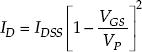
With increasing VDS the reverse bias towards the drain end increases, with increasing depletion region widths near the drain end. Ultimately, at some VDS the two depletion regions merge and drain current remains constant. This drain to source voltage beyond which the drain current tries to remain constant is known as the pinch-off voltage VP.

where, 2a = breadth of the channel towards the depletion regions
εS = Dielectric constant of the semiconductor material
εS = 12 ε0 where ε0 = permittivity of free space.
- Features of MOSFET
MOSFET devices have either built-in channel (DE MOSFET) or induced channel (MOSFET) for the device functioning. Voltages between gate and the source terminals VGS through capacitor action vary the carrier concentrations (electrons for N-type channel MOSFET or holes for P-type channel MOSFET) in the channel. This turn varies the conductivity of the channel and the device currents or channel currents.
The gate electrode is isolated or insulated from the other electrode structures. So, the input and the output ports are isolated with MOSFET amplifiers. The device is also known as IGFET. The MOSFET device consists of metal, silicon dioxide layer as insulator; N-type or P-type semiconductor substrate to form the source and the drain islands and a channel containing either electrons or holes as current charge carriers to modulate the conductivity of the channel
ID = K.[VGS − VTH]2where, K depends on the device structure
and VTH is the threshold voltage for device conduction.
MOSFET circuits occupy less space on silicon wafer and consume less power than the BJTs. They are suitable for VLSI circuits, such as CPU, RAM and a variety of ICs in practical circuits.