Chapter 2
Semiconductor Diodes and Rectifiers
2.1 Introduction
For proper understanding of the semiconductor or electronic devices in their various applications in electronic circuits used in electronic gadgets and systems (appliances), knowledge of the characteristics of the electron and its associated structures of atoms, energy levels and material properties is essential. So, the electronics subject will be developed step by step starting from the knowledge of electron behaviour in semiconductor devices, under the influence of electric and magnetic fields.
All matter is composed of molecules, which are the smallest particles preserving the individual characteristics of the substance. Molecules are composed of atoms and atoms are made of still smaller particles. According to the normal simplified theory, which will be sufficient for understanding the electron motion through solid semiconductor medium, an atom can be pictured to have a model as shown in Fig. 2.1. An analogy can be drawn to the planetary motion in which the planets rotate round the sun.

FIGURE 2.1 Electronic configuration of silicon atom
2.2 Electronic Configuration
The shell structure and states occupied by electrons depend on the valance of the material and its atomic number. The tetravalent materials Si and Ge that are used in the manufacture of semiconductor devices will have the structure represented in Table 2.1.
TABLE 2.1
| Element | Atomic Number | Configuration |
|---|---|---|
Si |
14 |
1s2 2s2 2p6 3s2 3p2 |
Ge |
32 |
1s2 2s2 2p6 3s2 3p6 3d10 4s2 4p2 |
The distribution of electrons in the various orbits for silicon atom is shown in the Fig. 2.1
2.3 Electronic Configuration of a Silicon Atom
The silicon atom consists of a nucleus (nucleus is a very complex body, containing positive charge and contains nearly all the mass of the atom). Surrounding this central positive core are the negatively charged electrons moving about it in closed orbits and are arranged as shown in the Fig. 2.1.
The orbits of the electrons in the planetary model of the atom are assumed to be concentric circles.
For silicon atom with atomic number Z = 14; the atom contains 14 positive charges in the nucleus and 14 electrons moving in various orbits; with the first orbit accommodating 2 electrons, second orbit, 8 electrons and third orbit the remaining 4 electrons.
The atom is electrically neutral. Hence, the silicon material is an electrically neutral material. The planetary model for the atom is considered only from the classical model.
The force of attraction between the nucleus and the electron of the atom is given by
where, electronic charge q is in coulombs, the separation between the two particles r is in metres, the force F is in N and εo is the permittivity of free space.
Permittivity of the free space εO = 8.849 × 10⁻¹² farads/metre.
This force of attraction is counterbalanced by ![]() where m is the electronic mass (m = 9.109 × 10⁻³¹ Kg), V = speed of the electron in the orbit and the acceleration is
where m is the electronic mass (m = 9.109 × 10⁻³¹ Kg), V = speed of the electron in the orbit and the acceleration is ![]() and is directed towards the nucleus.
and is directed towards the nucleus.
Then, according to Newton’s second law of motion,
The potential energy of the electron at a distance r from the nucleus is ![]() and its kinetic energy is
and its kinetic energy is ![]() .
.
According to conservation of energy
where the energy, w is in joules.
Substituting the value ![]() from equation (2.2) into equation (2.3) results in,
from equation (2.2) into equation (2.3) results in,
The equation (2.4) is the relation between the radius and the energy of the electron. This also shows that the energy of the electron becomes smaller (that is, more negative) as it approaches closer to the nucleus.
Each atom of silicon, of atomic number Z = 14, has its electrons arranged in groups of energy levels or shells as shown in the Fig. 2.1. First orbit, the inner-most energy level has 2-electrons, second orbit has 8-electrons and the third orbit has the balance 4-electrons. The inner energy levels containing two and the eight electrons are completely filled. Third energy level containing 4-electrons is partially filled. This last shell is called valence shell. The 4-electrons in the outer shell are known as valence electrons. Valence electrons are responsible for the chemical and electrical properties of the material. Electrons extracted from valence shell and are not subject to force of attraction of nucleus on them, are called free electrons.
So, the silicon atom is represented as shown in the following Fig. 2.2 for understanding the covalent bond formation, and so on.

FIGURE 2.2 Silicon atom
2.4 Electronic Configuration of a Germanium Atom
On similar lines it is known that germanium semiconductor atom of atomic number Z = 32 has 32-electrons in shells containing 2,8,18 and 4 electrons. Germanium material has chemical and electrical properties similar to silicon because of the four electrons in the outer incomplete shell.

FIGURE 2.3 Electronic configuration of Germanium atom
First, second and third orbits are completely filled and the outer shell is partially filled. Silicon and germanium materials are referred as tetravalent materials, since the valence electrons are four in number. The Germanium atom is shown in the following Fig. 2.4 for understanding the formation of covalent bonds, and so on.

FIGURE 2.4 Germanium atom
2.5 Energy Band Concepts of Materials
The electronic energy levels for a single free atom in a gaseous medium are descrete, since the atoms are sufficiently far apart, and the energy levels of individual atoms are not perturbed. The atoms in solid media such as crystalls, the energy levels of inner shell electrons are not appreciably affected by the neighbouring atoms. The energy levels of the outer shell electrons are changed due to the influence of neighbouring nuclei allowing sharing of electrons by more than one neighbouring atoms in the process of getting on to stable 8-electron configuration in the silicon and germanium semiconductors by forming covalent bonds. The sharing of outer shell electrons to form covalent bonds is shown in the Fig. 2.5.
The coupling between the outer shell electrons of the atoms results in a band of closely spaced energy levels or states instead of the widely spaced energy levels of the isolated atoms. Because of the coupling between atoms in crystals, completely filled and partially filled energy levels are merged into an energy band (as the interatomic distance is quite small in solid materials).
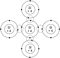
FIGURE 2.5 Covalent bonds about silicon atoms
Merging of empty energy levels form a conduction band. The lower most energy level of conduction band is considered as Ec. The completely filled and partially filled energy levels group into valence band. The top most energy level of valence band is considered as Ev. Energy gap between the conduction and valence band is known as forbidden band gap EG, which is equal to (Ec−Ev). The energy associated with the energy levels in electron volts plotted is shown on Y-axis and momentum (P) is on X-axis. The energy is measured in eV (electron volts). The unit of electron volt is the energy acquired by an electron while falling through a potential difference of 1 volt.
According to quantum-mechanical theory, when the energy band has all filled energy levels, the electron there cannot contribute to electrical conduction. There is no open energy level to which they can move after absorbing any energy from the applied electric field. Therefore, they do not absorb energy and do not become conduction electrons. Only the band containing the unfilled or empty energy levels is the conduction band.
The conductivity of a pure semiconductor at absolute zero temperature is zero, since the lower valence band is filled and there are no electrons in the upper conduction band.
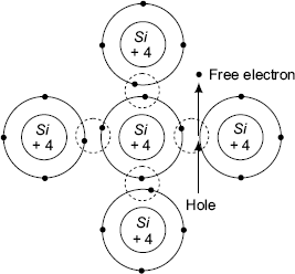
FIGURE 2.6 Formation of hole-electron pair
At the ambient temperature, some electrons may acquire sufficient energy equal to or greater than the forbidden band gap energy EG and will transfer to energy levels in the upper band. These electrons will be in an incompletely filled band and they can contribute to conduction. While the electrons move to the conduction band, they leave holes in the valence band (the holes were formed due to the formation of hole-electron pairs during the process of breakage of covalent bonds in valence band).
The conductivity of an intrinsic semiconductor is due to the hole-electron pairs formed during broken covalent bonds or due to supply of energy to free electrons to cross the forbidden band gap.
The resistivity of a semiconductor can be expressed as,
where A is a coefficient, varying slightly with temperature, ρ the resistivity of the semiconductor material, a function of temperature and forbidden band gap energy ∆EG.
The energy-band diagrams (in terms of momentum ![]() = K.E.) that follow in the figures from 2.7 to 2.10 describe the classification of materials into conductors, semiconductors and insulators.
= K.E.) that follow in the figures from 2.7 to 2.10 describe the classification of materials into conductors, semiconductors and insulators.
Conductors
Materials with adjacent or overlapped conduction and valence bands with zero forbidden band gap energy are known as conductors.
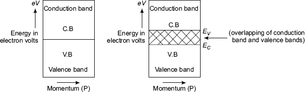
FIGURE 2.7 Energy band diagrams for conductors
Semiconductors
Materials with small forbidden band gap energy (EG) around 1 eV, are called semiconductors.
At 0 Kelvin, EG0 = 1.21 eV for silicon semiconductor material and for germanium semiconductor, EG0 = 0.785 eV
At room temperature (300 K), EG = 1.1 eV for silicon semiconductor and EG = 0.72 eV for germanium semiconductor.
where, EG is the forbidden band gap energy, Ec is the energy of the lower most level of the conduction band and Ev is the energy of the upper most energy level of the valence band.
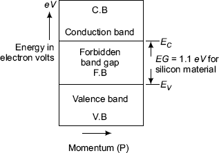
FIGURE 2.8 Energy band diagram for silicon semiconductor
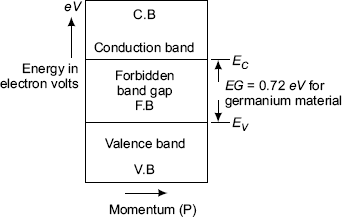
FIGURE 2.9 Energy band diagram for germanium semiconductor
Insulator
Materials with large forbidden band gap energy EG > 6 eV, those do not support conduction at all are known as insulators.
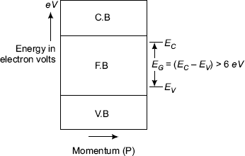
FIGURE 2.10 Energy band diagram for insulators
Conduction in Intrinsic Semiconductors
Purest semiconductor is known as an intrinsic semiconductor. At 0°K, semiconductor behaves like an insulator, because energies of the order of EG cannot be acquired from an electric field. At room temperature, covalent bonds in the semiconductor may be broken into a few hole-electron pairs, contributing to current flow through the material and so the conductivity increases.
As the temperature increases, some of the valence electrons acquire thermal energy greater than EG and so, they move into conduction band. These free electrons can move about under the influence of a small electric field. Dots or small dashes represent these free or conduction electrons.
The absence of an electron from covalent bond in the valence band is called a hole and is represented by a small hole or circle. Hole also serves as a carrier of electricity, comparable in effectiveness of an electron.
With respect to energy, if the electron is given additional energy, it breaks away from its covalent bond. When the free electron enters a hole in a valence band, this excess energy is released as a quantum of heat or light. In turn, this quantum of energy may be reabsorbed by another electron to break its covalent bond and create a new hole em electron pair. Thus, holes and electrons appear to move.
The conduction by holes is less when compared to that of electrons because of differences in freedom of movements for holes and electrons, based on their mobility. The mobility of electrons μn, is greater than the mobility of holes μp because of the differences in relative masses of electrons and holes, and due to the mechanism involved in their movement.
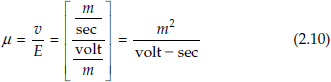
The mobility μ of electrons and holes is defined as the velocity acquired by these charged particles per unit applied electric field.
Electrical conduction by electron-hole pairs generated by thermal energy is called intrinsic conduction in the pure semiconductors, of either silicon or germanium.
2.6 Conduction in Conductors and Semiconductors
Mobility (μ)
In good conductors like metals, free electrons exist in abundance. They are supposed to be accelerated under the influence of field as per ballistic (dynamics) laws. But in practice it is found that the electrons move with a constant velocity proportional to the field. The reason for this is the random nature of the electron movement involved in repeated collisions. Thus, losing energy is acquired due to acceleration. It is observed that the random motion of electrons when resolved in the direction of the field, the electrons acquire a constant speed called the drift speed v that is proportional to the field E (volts/metre) and velocity v is in metres/sec.
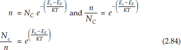
Thus, v = μE (2.9)
where μ is the constant of proportionality is termed the mobility measured in m2/volt-sec.
Current Density
Current density
where I is the current and A is the area of the conducting medium in m2.
Current density J, as current per unit area has the advantage, since the dimensions of the conducting medium are not directly involved. Now, the relation between current density and the charge density ρ can be arrived at.
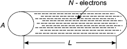
FIGURE 2.11
Current I (amperes) by definition is charge (coulombs)/time (seconds),
i.e.
where q is the charge of an electron and N is the number of electrons in a given volume. If the charge passes through a distance L (metres) in time T (seconds), then velocity v with which the electrons move is ![]() .
.
i.e.
Substituting the value of T from the equation (2.13) in equation (2.12), we get
![]()
That is, J = n.q.v, where n = ![]() is concentration of electrons, that is, the number of electrons per unit volume
is concentration of electrons, that is, the number of electrons per unit volume
Using v = μE, in the above expression,
Conductivity
The equation (2.17) derived in the previous section can also be written as
where σ is called as conductivity.
Here, it is found that the relation between current density and field strength, is as being proportional to each other with σ as the constant of proportionality; since J ∝ I and E ∝ v it is found that σ has the dimensions of Siemens/metre as shown.
![]() where g is conductance and r is the resistance.
where g is conductance and r is the resistance.

Conductivity of electrons,
Current density of electrons,
As already explained, semiconductors contain two types of mobile charge carriers, electrons (negative charge carriers) and holes (positive charge carriers). So, in semiconductors, the conductivity depends on the concentrations and mobility of both electrons and holes.
Conductivity of semiconductors;
where n = electron concentration;
μn = electron mobility; p = hole concentration; μp = mobility of the hole
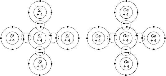
FIGURE 2.12 Covalent bonds in silicon and germanium semiconductors
Conduction in Semiconductors (Covalent Bond Structure)
Fourth group materials like germanium, silicon, and so on, contain four valence electrons in their outer most orbits. In a solid structure as shown in Fig. 2.12 each nucleus sees around itself 8-electrons in the outer most orbit, four of its own and four more, one each from the four of the neighbouring atoms to obtain 8-electron stable configuration. This electron pairing is called covalent bonding.
At room temperature of 300 K, It requires an energy of EG = 1.1 eV for breaking of covalent bonds in silicon material and EG = 0.7 eV to break the covalent bonds in germanium material and some electron-hole pairs are produced. Even at room temperature a few of the covalent bonds will be broken leading to existence of equal number of electrons and holes in conduction band and valence band, respectively.
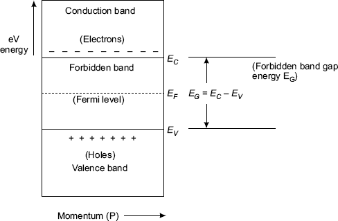
FIGURE 2.13 Energy band diagram for an intrinsic semiconductor
Fermi Level
The highest occupied energy level of an electron in a conductor is called Fermi level, EF. In the discussion of electron contributed conductivity, a few electrons within the reach of EF are supposed to contribute.
An energy level called Fermi level indicates the conductivity of a material. It is an energy level at which the occupancy is with 50% probability even at 0 K. This level is a real level in conductors but a virtual level in semiconductors, where an energy gap exists between conduction band and valence bands. Fermi level is a statistical quantity useful in determining the behaviour of materials in general.
In intrinsic or pure semiconductors like germanium and silicon, the Fermi level falls midway between conduction and valence bands. That is at the centre of the forbidden energy gap as shown in Fig. 2.13.
Temperature Sensitivity of Semiconductors Since increase in temperature causes extra energy supply, the conductivity σ of the semiconductor increases with temperature as more and more covalent bonds are ruptured. The energy gap decreases as is given by the following expression.
For germanium semiconductor, it is given by the following equation:
- EG(T) = 0.785 − (2.33 × 10⁻⁴) T. At room temperature EG = 0.72 eV for germanium semiconductor.
- EG(T) = 1.21 − (3.6 × 10⁻⁴) T. At room temperature (300 Kelvin) EG = 1.1 eV for silicon semiconductor.
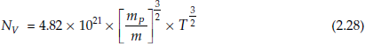
Thus the intrinsic concentration ni of charges is a function of temperature in the semiconductor materials and is expressed by
where, Ao is constant independent of temperature
Ao = 4.82 × 10²¹/m3
EGO = Energy band gap at 0°K
EGO = 0.785 eV for germanium and EGO = 1.21 eV for silicon materials.
K = Boltzman’s constant = 1.38 × 10⁻²³ joules/°K.
T = Absolute temperature in °K.
At room temperature T = 300°K
for silicon semiconductor as already expressed.
In a pure semiconductor, the hole and electron concentrations are equal and the concentration is expressed as
This is called mass-action law.
Though the velocity acquired by a carrier depends on E-field through (v ∝ ε; ![]() = μ) mobility, its dependence on temperature is given by μ ∝ τ −η where η is a characteristic value of carriers.
= μ) mobility, its dependence on temperature is given by μ ∝ τ −η where η is a characteristic value of carriers.
2.7 Extrinsic Semiconductor (Doped or Impure)
If, the symmetry of an intrinsic semiconductor is disturbed, by adding pentavalent (donor) or trivalent (acceptor) impurities to the pure semiconductor the conduction abnormally increases and the conductivity depends more on the dopant atoms as explained below.
N-type Semiconductor (Donor Type Doping)
Adding pentavalent atoms like phosphorus or arsenic material atoms in very small quantities into pure semiconductors is known as doping. Its result is as shown in the Fig. 2.14. Impurity atoms form covalent bonds with neighbouring atoms. There are five valence electrons for the impurity atoms and there are only four valence electrons for the intrinsic materials, silicon or germanium atoms. One electron of phosphorus atom fails to find a place to form covalent bond in the symmetric structure and can be pulled out to become a free electron by potentials of the order of 0.05 eV as against 1.1 eV for the pure semiconductor. This occurs for even small doping levels of the order of one dopant atom per 100 million atoms of pure semiconductor material. The Conductivity of the impure Semiconductor can be increased doping and Vice Versa.

FIGURE 2.14 N-type semiconductor (donor type doping)
P-type Semiconductor
Similarly, if trivalent impurity atoms such as boron material atoms are introduced, the three peripheral electrons form covalent bonds with the neighbouring intrinsic material atoms leaving a natural vacancy (hole) as shown in the Fig. 2.15. Compared to the environment it has one electron less to form a covalent bond thus leaving a relative unit positive charge called a hole. These holes can knock off electrons from the neighbouring atoms with as small energy as 0.05 eV and create holes. Thus, the hole is transferred from one atom to the other virtually giving mobility to holes in P-type semiconductors. It is to be cautioned that the hole movement is indirect and conceptual.
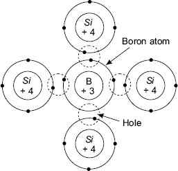
FIGURE 2.15 P-type semiconductor (acceptor type doping)
Structure of P-material As has been observed in the previous discussion, a P-material consists of mobile positive holes, one for each dopant atom (acceptor atom). However, the charge neutrality of the P-type semiconductor is retained, since for every hole, there is an associated negative charge in the covalent bond structure and it is said that the mobile positive charge covers the immobile negative charge. Thus, a pictorial representation for the P-material can be arrived as shown in the Fig. 2.16.
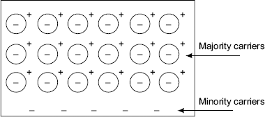
FIGURE 2.16 P-type material
Mobile and immobile charges in a P-type semiconductor In this the unencircled +ve charges represent mobile holes called covering charges, covering the immobile negative charges associated with the covalent bond structure. This results in charge neutrality, since every mobile hole covers the immobile negative ion. But the structure is not complete in the sense that there will be a few mobile electrons due to the broken covalent bonds of the intrinsic material. The mobile carriers generated (holes) due to doping will be many more compared with the intrinsic electrons. The mobile holes are called majority carriers. The mobile electrons are called the minority carriers. The point of interest to note is that the electrons in the P-type material will be less than what they would have been, had there not been doping. This can be justified as follows.
In a pure semiconductor there are as many holes as there are electrons and there is a certain probability of recombination between electrons and holes and yet in this process of generation and recombination an average concentration of electron—hole pairs exist. Now that doping increases the hole concentration of holes in a P-material, the probability of recombination increases and the minority carrier concentration decreases. The charge profile of majority carrier hole concentration and minority carrier electron concentration is shown in Fig. 2.17. Thus we see that from equal concentrations in a pure semiconductor, due to doping, the majority carrier concentration increases, while that of the minority carriers decreases. As shown in the Figs. 2.17 and 2.19, the ratio of new concentrations for majority and minority carriers is 1000. The majority carrier (hole) contributed current (typically of the order of 100 ma) can be accounted by being contributed by 6.25 × 10¹⁷ holes. Conspicuously, the minority carrier contributed current (a typical value of 100 μa) can be accounted by being contributed by a carrier number of 3 orders less (that is 6.25 × 10¹⁴).

FIGURE 2.17 Charge profile of P-type semiconductors
Structure of N-type Semiconductor In an N-type semiconductor, the mobile majority carriers are electrons covering the immobile positive charges (encircled). The mobile electrons cover the immobile positive ions and maintain electrical neutrality, as shown in Fig. 2.18. The few mobile holes represent minority carriers. Electrons are the majority carriers in N-type semiconductors.
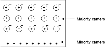
FIGURE 2.18 Mobile and immobile charges in N-type semiconductor
The charge profile of N-type semiconductor with majority carrier concentration of electrons and the minority carrier concentration of holes is as shown in the Fig. 2.19.
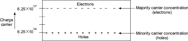
FIGURE 2.19 Charge profile of N-type semiconductor
2.8 Energy Band Representations of Doped Materials
The shift of the Fermi level (which is otherwise at the middle of the band gap in an intrinsic semiconductor) EFP towards valence band in a P-type semiconductor and the shift of EFN towards conduction band in an N-type semiconductor is comprehensible from the ongoing expressions for EFP and EFN in the following discussion.
Doping allows empty energy states in the hitherto forbidden band gap at the same level that is EA (acceptor energy level) (due to the dopant atoms being disseminated into the material and being so far away from each other excluding the possibility of interatomic influences). Now, for an electron to move from the valence band to an empty state, it need not travel all the way to the conduction band, but only up to acceptor energy level EA, which is very close to the boundary level Ev of the valence band. In this process, with a very little energy (even at room temperature) abundant numbers of holes are created in the valence band, thus increasing the conductivity of P-type semiconductor very much. Incidentally the minority carrier concentration decreases due to the inability of electrons jumping the forbidden band gap and entering the conduction band.
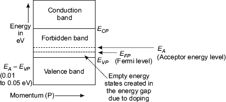
FIGURE 2.20 Energy band diagram for P-type semiconductor
The Fermi level moves closer to the valence band and has a quantitative expression
where mp and mn are the effective masses for holes and electrons, respectively, and m is the rest mass and NV correspond to constants for conduction and valence bands and are dependent on the effective masses of electrons and holes, and temperature as well.
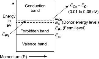
FIGURE 2.21 Energy band diagram for N-type semiconductor
In an N-type of semiconductor, the dopant atoms (pentavalent or donor impurity) contribute a discrete filled energy states all at one level ED (donor energy level) (as has been explained in P-type semiconductor) in the hitherto forbidden energy gap. Thus, to move an electron into the conduction band, a very small energy of the order of 0.01 to 0.05 eV is sufficient to pull the electrons into the conduction band, resulting in a highly increased conductivity. However, the hole production in the valence band decreases due to the lesser probability of electrons jumping into the conduction band creating holes.
The Fermi level moves up closer to Ec and have the value of
where

and,

2.9 Carrier Lifetime
The average concentration of electrons and holes in an intrinsic or pure semiconductor remains more or less constant and equal. However, there is a continuous process of generation of hole-electron pairs due to thermal agitation or irradiation and neutralisation due to the opposite charges meeting each other (hole-electron pairs disappear) in their random movements. This loss of electron-hole pairs is due to the phenomenon called recombination. Thus, an electron generated remains in the arena for a specific time called the mean lifetime τn before it disappears due to recombination. So, τn is called as carrier lifetime (for electron).
Similarly, τp is the lifetime for a hole. τp and τn have another significance, when applied to concentrations, for instance τp corresponds to the time taken for the excess concentration of holes to get reduced to 1/e of its enhanced value as shown in the Fig. 2.22. (due to irradiation). Carrier lifetimes range from a few nanoseconds to hundreds of microseconds.
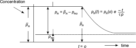
FIGURE 2.22 Variation of concentration of holes
p = Thermal equilibrium of minority hole concentration in N-type conductor. Total concentration of holes in N-material during the presence of radiation are as following:
In an N-material electrons are majority carriers and holes are minority carriers. If this N-type material is irradiated by say ultraviolet (UV) rays, equal number of electrons and holes are generated due to breaking of covalent bonds, because of the incident ultra violet energy and the concentrations go up to new values ![]() and
and ![]() for electrons and holes, respectively. But, this enhanced excess or injected concentration will be significant for minority carriers and quite insignificant for majority carriers. One can conclude that the excess injected carriers are of any consequence only for majority carriers. It may be logically deciphered from R-H-S (Reid-Hall-Shockley) theory or the underlining mechanism of recombination of irradiation generated excess carriers. As such, the current through the function is dominantly influenced by the leftover minority carriers on either sides of the function.
for electrons and holes, respectively. But, this enhanced excess or injected concentration will be significant for minority carriers and quite insignificant for majority carriers. One can conclude that the excess injected carriers are of any consequence only for majority carriers. It may be logically deciphered from R-H-S (Reid-Hall-Shockley) theory or the underlining mechanism of recombination of irradiation generated excess carriers. As such, the current through the function is dominantly influenced by the leftover minority carriers on either sides of the function.
If at time t = 0, ultra violet source is switched off, then obviously, the excess concentrations should come back to their thermal equilibrium values over time due to recombinations. As shown in the Fig. 2.22, pno represents the thermal equilibrium concentration of holes in N-material. Due to irradiation, pno becomes ![]() no.
no.
The excess concentration will become ![]() no = pno.
no = pno.
Let this be pn. Excess concentration = ![]() no – pno = pn.
no – pno = pn.
If at t = 0 the ultra violet source is switched off and pn is represented as pn(0).
Then, pn0 = ![]() no = pno at t = 0 and represents the excess minority carrier concentration, that is, holes in N-material.
no = pno at t = 0 and represents the excess minority carrier concentration, that is, holes in N-material.
Due to switching off the radiation that is the excess energy being removed, the excess concentrations disappear over time and return to their equilibrium values.
As shown in the Fig. 2.22
pn (0) = pn – pn0 will decrease exponentially with time given by the expression.
Similarly, for P-material, as the carriers move in a semiconductor material, they encounter opposite charges and recombine, thus decreasing the concentration with distance. Over a distance x, the charge of excess minority carrier concentration with distance can be represented by
where pn(x) is representative of excess hole concentration with distance, pn(0) represents the excess hole concentration at x = 0 and falls off exponentially. As represented in the above equation, Lp is called the diffusion length for holes. Lp represents the mean free path of a hole before it recombines with an electron. This is otherwise the distance at which the excess hole concentration falls off to a value 1/e of the concentration at x = 0.
Similarly
where np(x) is the concentration of excess minority electrons in the P-type semiconductors as a function of distance, np(0), the concentration at x = 0 and Ln is diffusion length for electrons as explained in Fig. 2.23.
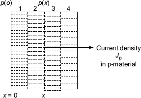
FIGURE 2.23 Diffusion
2.10 Diffusion
Fig. 2.23 shows a material in which the concentration is non-uniform and decreases with distance. This change in concentration with distance is called concentration gradient and allows charge movement because of concentration variation. This process of movement of charges from regions of greater concentration to regions of smaller concentration is called diffusion. Due to this charge movement, a current density Jp proportional to the concentration gradient ![]() appears and it is expressed as a relation.
appears and it is expressed as a relation.
where DP is the diffusion constant for holes, measured as m2/sec.
The negative sign in the equation (2.37) appears because of the fact that with distance x, the concentration is decreasing. Since electrons can be considered as duals of holes, current density for electrons due to concentration gradient ![]() ,
,
Einstein Relation
The mobility µ and diffusion D are both thermodynamic phenomena and a correlation should exist between them. Einstein has expressed this in the following manner. This goes under the name Einstein relationship.
Einstein relationship expresses the relationship between diffusion constant DP and mobility µ in the following manner:
VT is called voltage equivalent of temperature. The significance of VT can be explained as follows.
Since, temperature causes thermal agitation resulting in movement of charges; VT can be expressed as a voltage, which also causes movement equivalent to that produced by temperature and thus it is called as voltage equivalent of temperature.
Net Current
In the semiconductors drift current exists due to potential gradient and diffusion current due to concentration gradient. Since both are independent and coexist, the total current should be the algebraic sum of both these currents as expressed below:
For holes,
and, for electrons,
Continuity Equation
Let an elemental volume V = A.dX of a semiconductor material be considered. Due to ambient temperature electrons and holes are continuously generated. These charges move randomly through the volume. During the movement electrons and holes encounter each other and recombine.
Since, the semiconductor has some finite resistance, which is not infinite some free charges should be available. This implies that the generated hole-electron pairs are more than those lost in recombination. So, there can be a net charge flow in a specific direction, for example, in the X-direction, as shown in the Fig. 2.24. Movement involves time and distance. So, over a period of time there will be change in concentration, which depends on distance also.
The random movement of charges in a semiconductor at a given time may have a net flow of charge in one direction say, +ve direction. This causes a change in concentration along the length of the conductor, creating a concentration gradient. In other words, whenever there is a non-uniform doping concentration, it results in an inbuilt electric field gradient (P-d) within the semiconductor to give rise to a diffusion current. So, at two different points X1 and X2 along the X-direction in a conductor, there will be different amounts of charge accumulation. At one point say, X1, charge may be more than at the second point X2, where (X1 + dx) = X2, the charge may be less. This establishes a potential gradient (electric field). This potential gradient or an equivalent battery, opposes the further movement of the charges in that direction. The charge movement due to potential gradient or electric field is known as drift. The diffusion and drift processes are in constant opposition. Hence, the currents due to drift and diffusion processes will be equal and opposite, resulting in the conservation of charge over the volume.

FIGURE 2.24 Representation of charge flow in the volume of a rectangular cube of a semiconductor material
This law of conservation of charge (charges can neither be created nor destroyed) expressed as a relation is called the continuity equation. This implies that under no external excitation, the average current in the elemental volume is zero.
As shown in the Fig. 2.24, if the concentration of holes is p and τp is the mean lifetime of the hole, the number of holes lost due to recombination is ![]() per second so, the charge decreases within the same volume due to recombination.
per second so, the charge decreases within the same volume due to recombination.
The decrease in the charge within the volume V, is qAdx ![]() (2.42)
(2.42)
If due to thermal agitation, an amount of g electron-hole pairs are generated per second, increase in charge within the volume is qAdx.g. (2.43)
In general, the current should vary with distance in a semiconductor material and if I amperes of current enters the considered volume at x1 and (I + ΔI) leaves the volume at x2; the decrease in charge in coulombs per second contributes to a current of magnitude dI (2.44)
The combined effect of all the above three processes shown by the equations, 2.42, 2.43 and 2.44, is to increase the total charge density and the number of coulombs per second.
This increase in charge within the volume V is qAdx ![]() (2.45)
(2.45)
Applying the law of conservation of charge to the above three processes, the following equation (2.46) is obtained.
where – qAdx × ![]() is due to recombination
is due to recombination
qAdx × g – dI is due to thermal generation of charges.
The net whole current should be the sum of the diffusion current and the drift current as discussed earlier
![]()
where – ![]() is the diffusion current and qApµpE (2.49) is the drift current.
is the diffusion current and qApµpE (2.49) is the drift current.
In equation (2.49), E is the field intensity within the volume.
Under equilibrium conditions, with no external excitation, the hole density should be a constant.
Let this be PO
So,
Substituting these values in the following equation (2.50)
the result becomes
From the equation (2.47), ![]()
or,
Substituting this in the equation (2.46)
Since the concentration p is a function of time, distance and field, partial differentials should be used.
So,
Solutions of the continuity equation for different boundary conditions yield very useful results. The equation (2.54) is called the continuity equation and by applying various boundary conditions, different results relating to the behaviour of semiconductor devices can be obtained.
2.11 Hall Effect
It has been observed that when a slab of metal or semiconductor material carrying a current I (say in X-direction) is placed in a magnetic field B Teslas, where B is perpendicular to the direction of current I (say in Z-direction), an electric field, ε volts/metre was observed across the faces F1 and F2 of the semiconductor slab in a direction perpendicular to both I and B ((ε) in Y-direction) as shown in Fig. 2.25.
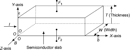
FIGURE 2.25 Illustration of Hall effect phenomenon
The appearance of the voltage VH across the two faces F1 and F2 of the semiconductor slab is called as Hall effect. The voltage VH is called as the Hall Voltage.
where, |
T is the thickness of the semiconductor slab |
|
VH is Hall Voltage |
|
ε is the electric field. |
The appearance of the Hall voltage, VH, can be explained as follows. Due to the current I flowing through the slab situated in a transverse magnetic field B, a force F is to be exerted in a direction perpendicular to both B and I on the charges in the slab. So, the charges migrate towards the top face F1 or bottom face F2 depending upon the polarity of the charge. If the current carriers are the electrons, they migrate towards the bottom face F2 for the assumed direction of flow of the current. The assumed current I may be due to holes moving from left to right or due to free electrons moving from right to left through the semiconductor slab. Thus, the upper face F1 will be positive with respect to the bottom face F2. The charge carriers in the semiconductor slab will be electrons if the material is N-type material and the polarity of the VH is such that F1 will be positive with respect to F2. Thus, if the Hall voltage VH between F1 and F2 is such that F1 is +ve, the inference is that the material is of N-type semiconductor.
By extending the same logic, a P-material can be identified by the polarity of the Hall voltage being in reverse direction with F1 being negative and F2 being positive as the holes also move down towards face F2.
The force exerted on the electrons is
where |
q is the charge of the carrier |
|
ε is the electric field |
|
B is the magnetic field |
|
v is the drift speed. |
In the equilibrium state, the electric field intensity ε due to the Hall effect must exert a force on the carrier fVH = eε, which just balances the magnetic force fB = Bev.
Therefore, qε = Bqv (2.57)
where v = drift speed
![]() (where T is the thickness of the semiconductor slab, or the distance between the two faces or surfaces 1 and 2 of the semiconductor slab).
(where T is the thickness of the semiconductor slab, or the distance between the two faces or surfaces 1 and 2 of the semiconductor slab).
where ρ is charge density
w is width of the metal or semiconductor specimen in the direction of the magnetic field B (and in this case Z-direction)
Using v = J/ρ in the above equation
If VH B, w and I are measured, the charge density ρ can be determined using the equation
(Note: Apart from the fact that the equation (2.61) expresses VH in terms of B, I, ρ and w, the practical way of measuring VH involves directional notation also.)
If the polarity of VH is + ve at terminal F1 then carriers must be electrons and ρ = ne, where n is the electron concentration. If on the other hand, terminal F2 becomes charged positively with respect to terminal F1, the semiconductor must be P-type and ρ = p.e where p is hole concentration. Using this concept of Hall effect, the semiconductor materials can be identified as P-type or N-type semiconductors. The concentration and the nature of charge carriers in the materials can also be determined in this process.
By definition, Hall coefficient
Hence,
If the conduction in the material is primarily due to the charges of only one sign, the conductivity is related to mobility.
If the conductivity is measured together with the Hall coefficient, the mobility μ of charge carriers can be determined from the equation
We have assumed in all the discussions that all particles travel with the mean drift velocity v (drift speed v). Actually, the current carriers have a random distribution in speed. If this distribution is taken into account, it is found that equation (2.63), ![]() remains valid, provided that RH is defined by
remains valid, provided that RH is defined by ![]()
Substituting value of RH from equation (2.66) into (2.65),
2.12 P-N Diode
When a P-material and an N material are brought into contact some processes start.
In P-type semiconductor material, holes are the majority carriers and electrons are the minority carriers. In P-material block, holes are in excess as they are majority carriers. But yet the material is neutral because every mobile hole is associated with an immobile negative charge (covering). Similarly in N-type semiconductor, electrons are the majority carriers and the holes are the minority carriers. In the N-material block, electrons constitute the majority carriers covering the immobile positive charges (charge neutralization) as shown in Fig. 2.26.
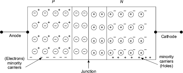
FIGURE 2.26 P-N junction with open circuit or no external excitation
Because of the contact between the two blocks of P and N materials, diffusion processes start. This is because of excess majority carriers that are holes on the P-material side, face very few holes (minority carriers) on the N-material side, resulting in a concentration gradient. This incidentally builds a charge gradient as well, as shown in the Fig. 2.27
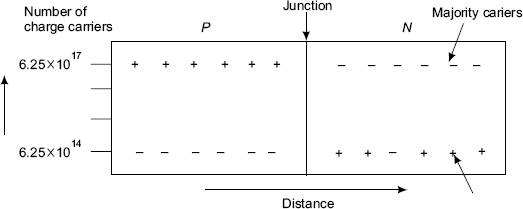
FIGURE 2.27 Concentration of holes and electrons in p-type and N-type materials. Charge profiles for illustrating the concept of charge gradients
This Fig. 2.27 represents the concentrations of holes and electrons in P-type and N-type materials on both sides of the junction of the semiconductor diode. The concentrations are indicated by the profiles, where Y-axis represents concentrations of the current carrying charge carriers and X-axis represents distance. Here, uniform concentration is assumed in the P and N materials. The concentration gradient among holes on either side of the junction makes the holes in the P-material move towards the N-material crossing the junction of the two materials. Similarly, the concentration gradient among electrons on either side of the junction causes the electrons in the N-material move towards the P-material crossing the junction. However, this process cannot continue forever.
As the holes and electrons migrate into the other regions, the hitherto covered immobile ions on either side of the junction get uncovered. The mobile charges encountering the opposite charges may recombine leaving a no-mobile charge domain nearer the junction. This region, deplete of mobile charges is called the depletion region, transition region and space charge region.

FIGURE 2.28 Representation of covalent bonds with acceptor and donor impurities (hole and excess electron representation)
The uncovered immobile charges (immobile ions) develop a potential gradient with fixed negative charge on the P-side and fixed positive charge on N-side. The tendency of this charge is to oppose movement of electrons into the P-region (mobile negative electrons encountering immobile negative ions). The same thing happens to the holes trying to move into N-side. Still, the migration continues further till the immobile charges are sufficiently strong enough to prevent further progress of mobile charge movement. An equilibrium condition is established which creates a barrier for further movement of mobile charges. This barrier potential is also known as space charge potential, depletion potential, transition potential, and contact or built-in potential. Any trial, on the part of the carriers to move further results in the increase of barrier potential preventing movement. Similarly, any decrease in movement causes the barrier potential to fall, thus, encouraging enhanced movement. To sum up, the increase or decrease in movement as well as the increase and the decrease of barrier potential are both prevented and a dynamic equilibrium is established. This happens when the current due to drift and the current due to diffusion are equal and opposite. The magnitude of the depletion potential is dependent on the relative doping on each side of the junction. The no charge region or depletion region spreads more into less doped material and less into more doped material. The reason is obvious since to get the same uncovering of immobile ions requires more penetration into the less doped region, whereas it requires less deep penetration into the more doped region.
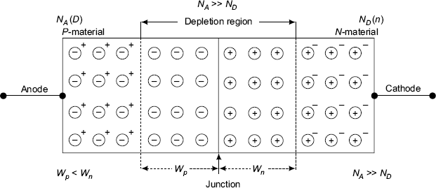
FIGURE 2.29 Depletion region widths in P and N type materials
Energy Band Diagrams for a P-N Diode with No Bias
Once P and N materials are brought into contact, the diffusion and drift processes start and equilibrium is reached till the Fermi levels on both sides are aligned. As a result of the diffusion and drift mechanism, due to the formation of the diode junction and in the wake of possible shift of Fermi levels (as discussed earlier) the energy band diagram of a P-N diode may be representeed as in Fig. 2.30. This causes a potential difference Vo to be developed across the space charge region and is called the contact difference of potential or built in potential. The quantitative relation can be obtained in terms of energy level as follows. According to the diagram, the shift in energy levels
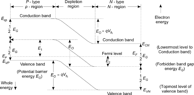
FIGURE 2.30 Energy band diagram of a P-N junction
This E0 represents the potential energy associated with the electrons at the junction.
Contact Difference of Potential E0 or V0
Rearranging the above equations,
From the Fig. 2.30, E1 + E2 + = E0 (2.73)
∴ E1 + E2 + = E0 = EG − EF + EVP − ECn + EF (2.74)
∴ E0 = EG + EVP − ECn (2.75)
From the following two equations (2.76) and (2.77)
And,
From the equations for P-type semiconductor npPp = ni2 (2.82)
(nP = concentration of electrons that is minority carries in P-material and Pp = majority carrier holes in P-material)
Since Pp = NA, equation (2.82) is written as in equation (2.83)
![]()
For N-material Ec = Ecn and n = ND
Substituting for Ec and n from the above equation into (2.85)
Similarly, the following equations can be obtained by suitable substitutions.
Substituting equations (2.81), (2.86), (2.87) into equation (2.75)

Since

Finally,
V0 depends on VT that is on temperature and also on the concentrations of P and N materials and the intrinsic concentration ni. As doping level increases V0 increases, and if doping is zero, as is the case with intrinsic semiconductor or any one type of extrinsic semiconductor, barrier potential V0 is zero.
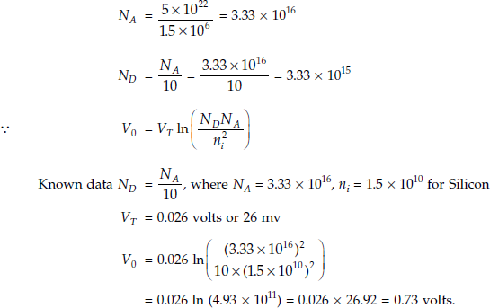
Calculation of built-in voltage V0 for silicon diode For instance, if NA = 10 ND and the doping level is such that there are 1.5 dopant atoms per million of intrinsic atoms for silicon; V0 at T = 300 K will be 0.7 volts as shown below.
Calculation steps
Number of atoms/cm3 of silicon material = 5 × 10²²
Open Circuited Junction of P-N Diode
When an intrinsic semiconductor wafer (like silicon or germanium) is doped by acceptor (P) and donor (N) impurities from either side a P-N junction is formed. Fig. 2.31 shows the formation of the materials. On the P-material side immobile negative charges and mobile positive charges (holes) appear. Similarly, on the N-material side immobile positive charges and mobile negative charges (electrons) appear. These mobile charges (majority carriers) cross the junction due to concentration gradient. This movement causes exposure of immobile charges, or ions on either side of the junction. On the P-material side, negative charges, which were neutralised by the mobile holes due to the migration of mobile holes get uncovered. The same thing happens with the immobile positive charges and the mobile electrons on the N-material side. This leads to the formation of a potential gradient. This is called as the contact, diffusion, barrier, depletion or space charge potential designated as V0.
In the absence of any excitation as explained earlier the contact potential V0 is developed at the junction of the P-N diode. In the profiles the various involved quantities (ρ = Number of uncovered ions/volume), charge density, electrostatic field intensity and potential energy barriers for electrons and holes at the junction contributing to the contact potential V0 are as shown in the Fig. 2.31.
The space charge region will be of the order of 0.5 micrometre thickness on either side of P-N junction point.
Variation of charge density is shown in Fig. 2.31 (b). This is a plot of
where, ρ = space charge density and ∊ = permittivity as obtained from Poison’s relation. Fig. 2.31 (c) represents the variation in field intensity across the junction and is given by
Fig. 2.31(d) represents the potential variation with distance, which is again ![]() In the N-material the potential raises from left to right reaching a maximum value of V.
In the N-material the potential raises from left to right reaching a maximum value of V.
Fig. 2.31 (e) represents the variation of potential from N to P side and is a complement of Fig. 2.31 (d). The field intensity ε is proportional to charge density and so on.
Forward Biased P-N (Junction) Diode
Considering the application of a potential difference to a semiconductor diode to make P-material side positive and N-material side negative from an external source Vf, the junction is considered to be forward biased (The D.C. source applying the voltage to the semiconductor diode is known as Bias voltage). The majority carriers, holes in the P-type semiconductor material now will be pushed towards the junction of the semiconductor diode due to the force exerted by the positive of Vf and enter the N region and the majority carriers, electrons from the N-type semiconductor material move in the opposite direction towards the junction and enter the P-material due to the force exerted by the negative of Vf. The barrier potential V0 is decreased by the amount of external bias voltage and hence constitutes a continuous current called forward current If. This situation happens when the forward bias voltage overcomes the restraining force by the contact or depletion potential or voltage V0,
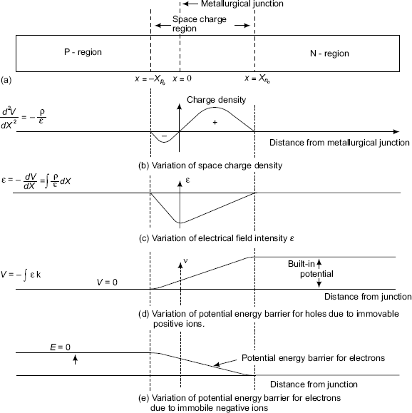
FIGURE 2.31 Sketches for distribution of charge density (ρ) electric field intensity (ε) and potential energy barriers (v) for holes and electrons in a P-N diode
Note: NA >> ND. As the doping is not symmetrical in practical diodes, the space charge region extends deeper into the lightly doped region. This depletion approximation is shown in figure (a).
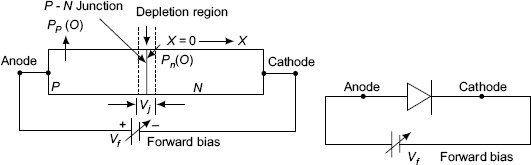
FIGURE 2.32 P-N junction diode with forward bias
The quantitative relationship between current and voltage will be obtained in the following manner.
From continuity equation we can obtain expression for the current by considering the net current due to drift and diffusion phenomena. The diffusion current is due to concentration gradient among the charge carriers on either side of the P-N junction and drift current is due to potential gradient. The diffusion current is due to holes (being the majority carriers) in the P-material crossing the P-N junction and becoming the minority carriers (injected carriers) in the N-material region. The injected minority carrier current or the excess minority carrier current into the N-material can be defined as following:
Ipn(0) represents the value of current at the P-N junction of the holes entering N-material region. This is actually Ipn (x) when x = 0, where x is distance from the junction.
On the P-material side Ppo represents the equilibrium majority concentration of the holes. As these enter the N-material region at the junction they become Pn (0).
This represents excess minority carriers (holes) injected from P-material into the N-material and add to the local minority carriers in the N-material with distance. This falls off exponentially due to recombination with the majority carriers (electrons). This is represented as follows:
[The above relation (2.91) is obtained as follows from continuity equation]. It is known that
At
where, p1n(0) represents excess minority carriers entering into the N-material region. When this equation (2.94) is substituted in the above equation (2.91), the resulting equation is
In the equation (2.95); p1n(0), that is the magnitude of the injected minority carriers depends upon applied electrical potential. The quantitative relationship between p1n(0) and V is going to be derived in the succeeding section.
The Law of Junction
Across the P-N junction of the semiconductor diode, the electric field is very high (because of very small space charge region of order of 0.5 micron.) The diffusion current is also very high due to very high concentration charge gradient. Since these oppose each other and large, the net current density will be very small. So, if the difference of these two large quantities is very small they should be very nearly equal
JP = Drift component of current – Diffusion component of current
The next step is to equalise these two; the drift component of current and the diffusion component of current, as per the above reasoning
![]()
Therefore, in the above equation (2.98) P represents the equilibrium concentration of holes on the P material. The holes enter at the P-N junction of the diode at x = 0 into the N-region and they become the injected minority carrier hole concentration. Notionally, the concentration of holes entering the N-region at the junction at x = 0 is termed as Pn(0). The junction voltage is (V0 – V); where V0 is the barrier or contact potential and V is the applied forward bias.
from equation (2.100),
Integrating the equation (2.101), the result is
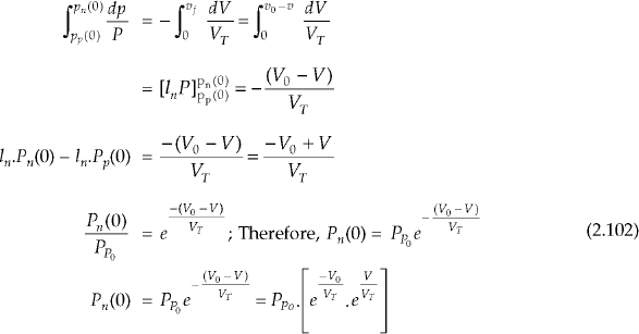
But it is known that ![]()
From the derivation for V0 in terms of concentration on P-material side and N-material side of the holes, where ppo represents holes in P- region pn0 represents injected minority carriers in N- region, under equilibrium conditions
or, ![]() or combining the equations, (2.102) and (2.103)
or combining the equations, (2.102) and (2.103)
Equation for law of junction (2.104) follows,
This equation, (2.105) is called as law of junction at the boundary of the P-N junction formed by the P-type and N-type semiconductor materials of the P-N diode. This law indicates that injected minority carrier hole concentration Pn(0) at the P-N junction into the N-material is obtained by multiplying the equilibrium minority concentration Pn0 by ![]() . That is, the injected carrier current due to holes Pn(0) exponentially increases with respect to applied forward bias voltage V.
. That is, the injected carrier current due to holes Pn(0) exponentially increases with respect to applied forward bias voltage V.
2.13 Current Components in the P-N Semiconductor Diode
Consider a semiconductor diode (P-N diode) applied with forward bias voltage V. Holes are pushed into the N-type semiconductor region and electrons are pushed into the P-type semiconductor region. The number of charge carries that move through the semiconductor materials on either side of the P-N junction contribute to various components of currents as explained in the following section. At the same time it is to be remembered that the magnitudes of currents, under the application of voltages to the P-N diode, increase or decrease along with charge distributions.
Consider the charge flow in the N-material region due to the injected (excess) minority carrier hole concentration pn1 (0); equilibrium minority carrier holes Pn0 and Pn(0), the total minority carriers.
pn1 (0) is excess minority carriers entering N-type region = Pn(0) – Pn0
where, |
pn(0) = total minority carriers |
|
Pn0 = equilibrium minority carriers in the N-type region |
So, the total should be the sum of the above.
∴ Pn1(0) = Pn(0) − Pno (2.107)
Using the equation (2.105) for law of junction, ![]() in equation (1.107),
in equation (1.107),

Similarly, the majority carrier electrons crossing from N-region into P-region constitute a current Inp (0) as mentioned in the equation (2.112)
The total current I contribution from the semiconductor diode is the sum of the two quantities Ipn (0) and Inp (0) due to the holes moving from P-material to N-material contributing to current Ipn (0) from P-side to N-side and the current Inp (0) from P-side to N-side due to the movement of electrons from N-material to P-material through the semiconductor diode considered from the equations (2.111) and (2.112). These two currents Ipn(0) and Inp(0) being due to opposite charges (holes and electrons) moving in opposite directions become additive.
Hence, I = Ipn(0) + Inp(0) (2.113)

Equation (2.115) can be generalised as
where η = 1 for germanium diode and η = 2 for silicon diode.
where
I0 is called the reverse saturation current.
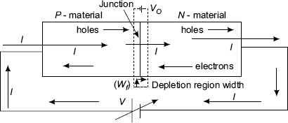
FIGURE 2.33 P-N semiconductor diode with forward bias voltage V
If the applied voltage V is positive (positive terminal of the voltage source V connected to P-material side and negative terminal of the voltage source V to the N-material side of the P-N diode to forward bias the device) and is much greater than VT, then ![]() and represents forward bias situation for the current I to become If; for the forward biased semiconductor diode.
and represents forward bias situation for the current I to become If; for the forward biased semiconductor diode.
This condition is basically obtained since ![]() at T = 300°. On the other hand, for V >> VT with V positive the current I increases exponentially with voltage. The junction potential or the built-in voltage or barrier voltage becomes actually,
at T = 300°. On the other hand, for V >> VT with V positive the current I increases exponentially with voltage. The junction potential or the built-in voltage or barrier voltage becomes actually,
as already explained. V0 is contact potential and V is applied external potential. If V is positive, junction potential will be decreased by the amount V from Vo and the barrier height is lessened (contact potential or barrier voltage V0 is reduced with a consequence of reduction in the depletion region width Wf). The discussion by now makes it clear that the current I known as the forward current If through the forward biased semiconductor diode is mainly due to the flow of majority carriers through the device. In a forward biased P-N diode, the forward current If enters the P-material side as hole current and leaves the N-material side as electron current of the same magnitude.
On the other hand, If V is negative and >> VT then the current through the device, I = – I0, since ![]() written | V | >> VT is negligible which means that under reverse bias condition the current reaches a saturation value I0; if | V | >> VT
written | V | >> VT is negligible which means that under reverse bias condition the current reaches a saturation value I0; if | V | >> VT
If V is negative,
So, the barrier height is raised with a consequence of increase in the depletion region width about the junction of the P-N diode.
In Fig. 2.34, negative terminal of the voltage V is connected to the P-material and positive terminal of the voltage V is connected to the N-material of the P-N diode. This makes the P-N diode applied with reverse bias voltage. The majority carriers holes from the P-material and the majority carriers electrons from the N-material move away from the P-N junction, thereby uncovering more immobile charges near the junction resulting in more immobile ions about the junction. Therefore, the barrier potential V0 and the depletion region width (Wr) are increased as shown by the mathematical expression (2.118). The reverse saturation current I0, flows through the diode from N to P materials due to the movement of minority charge carriers through the device. From Fig. 2.17, the charge profiles in the materials of the P-N diode, the number of minority carriers are very small. Hence, the reverse saturation current I0 or Ir or IS is negligibly small and is of the order of a few microamperes for a germanium device and a few nanoamperes for a silicon device.
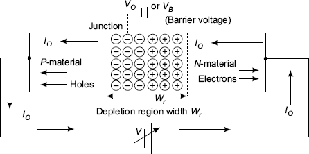
FIGURE 2.34 Semiconductor diode with reverse bias voltage V
2.14 Characteristics of P-N Diode
Forward Biased P-N Diode Characteristics
In Fig. 2.35 Vf is the actual voltage across the P-N diode that applies the forward bias to the P-N diode, because of the use of the current limiting resistor RL in the circuit. When the diode is forward biased, till the voltage Vf reaches a particular value, conduction does not start, which can be seen from the expression ![]() and also the forward characteristic as shown in Figs. 2.35, 2.36 and 2.37.
and also the forward characteristic as shown in Figs. 2.35, 2.36 and 2.37.
This feature of semiconductor diode conduction when the device is forward biased can be explained qualitatively by considering the two components of field intensity on the majority charge carriers on either P or N type semiconductor materials. One, field component ![]() tries to push the majority carriers, say, holes in P-material into N-material, while the field component
tries to push the majority carriers, say, holes in P-material into N-material, while the field component ![]() due to positive immobile ion charge in N-material due to space charge about the junction will try to restrain the entry of holes from P-material into N-material as long as εVf is less than εV0. But once εVf is larger than εV0, holes from the P-material enter the N-material and continue their journey to negative terminus of external voltage. However, so generated paucity of holes on P-side of the junction is supplemented by the positive terminus of the external voltage as to promote continuous flow of charge carriers through the device and the circuit. This contributes to the forward current If (similar will be the situation for majority carrier electrons from the N-material). This minimum forward bias voltage required for the diode conduction is known as the cut-in voltage Vγ or off-set voltage or the threshold voltage. The magnitude of this cut-in voltage is of the order of 0.2 to 0.3 volts for germanium semiconductor diodes (semiconductor devices in general) and 0.5 to 0.7 volts for silicon semiconductor diodes. In this process, the forward bias reduces the depletion region width as shown in Fig. 2.34.
due to positive immobile ion charge in N-material due to space charge about the junction will try to restrain the entry of holes from P-material into N-material as long as εVf is less than εV0. But once εVf is larger than εV0, holes from the P-material enter the N-material and continue their journey to negative terminus of external voltage. However, so generated paucity of holes on P-side of the junction is supplemented by the positive terminus of the external voltage as to promote continuous flow of charge carriers through the device and the circuit. This contributes to the forward current If (similar will be the situation for majority carrier electrons from the N-material). This minimum forward bias voltage required for the diode conduction is known as the cut-in voltage Vγ or off-set voltage or the threshold voltage. The magnitude of this cut-in voltage is of the order of 0.2 to 0.3 volts for germanium semiconductor diodes (semiconductor devices in general) and 0.5 to 0.7 volts for silicon semiconductor diodes. In this process, the forward bias reduces the depletion region width as shown in Fig. 2.34.

FIGURE 2.35 P-N semiconductor diode with forward bias voltage, V

FIGURE 2.36 Forward biased P-N diode circuit
When ![]() is much less than 1, only a very small current results. But, when once the forward bias voltage Vf is sufficient enough to make relatively larger than VT; the forward current If starts rising suddenly and reaches abnormal magnitude, unless limited by using a limiting resistance RL. As seen from the characteristic in the Fig. 2.37, as the junction potential reaches V0, the current increases exponentially. This minimum potential before which the forward current If is negligible is termed Vγ, known as cut-in voltage, offset voltage or threshold voltage depending upon the application of the semiconductor diode. It is about 0.5 to 0.7 volts for silicon diode and 0.2 to 0.3 volts for germanium diode at T = 300 K.
is much less than 1, only a very small current results. But, when once the forward bias voltage Vf is sufficient enough to make relatively larger than VT; the forward current If starts rising suddenly and reaches abnormal magnitude, unless limited by using a limiting resistance RL. As seen from the characteristic in the Fig. 2.37, as the junction potential reaches V0, the current increases exponentially. This minimum potential before which the forward current If is negligible is termed Vγ, known as cut-in voltage, offset voltage or threshold voltage depending upon the application of the semiconductor diode. It is about 0.5 to 0.7 volts for silicon diode and 0.2 to 0.3 volts for germanium diode at T = 300 K.
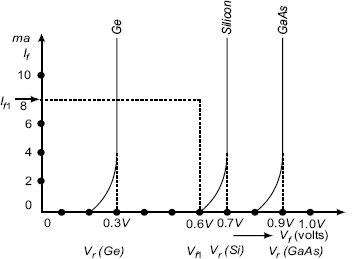
FIGURE 2.37 Forward characteristics for germanium, silicon and gallium arsenide diodes
For a P-N junction diode the diode current
where η = 2 for silicon diode for small currents and η = 1 for large currents and for germanium diode η = 1 at both small and large currents. It is interesting to note that the η = 2 in the expression for silicon diode decides the rate of rise of current in the vicinity of cut-in voltage to be used as shown in Fig. 2.37.
The inverse slope of the If – Vf characteristic is called forward resistance, Rf, which is of the order of a few ohms to a few hundred ohms, and will be virtually negligible in many cases in electronic application. Hence, a forward biased semiconductor diode acts as a closed electrical switch.
Forward resistance Rf, is the ratio of forward voltage, say Vf to forward current If at a point as shown on the diode forward characteristic. As an example shown in the Fig. 2.37; If Vf1 is equal to 0.6 volts and If1 is equal to 8 ma, then forward resistance of the diode is equal to 75 ohms.
Reverse Biased Semiconductor Diode Characteristics
When a diode is reverse biased by Vr as shown in the Fig. 2.38; the current Ir will be of the order of a few nanoamps for silicon diode and a few μA for germanium diode; because the reverse current Ir is due to the flow of minority carriers through the devices. The current IO or IS known as the reverse saturation current is independent of the reverse bias voltage up to a certain value and suddenly shoots high resulting in the breakdown of diode. The voltage at which the diode breaks down is known as breakdown voltage Vbr. This breakdown voltage rating will be provided in manufacturer’s data manuals of the semiconductor diodes. Under normal circumstances this region is inoperable.

FIGURE 2.38 Reverse biased diode circuit
The sudden rise in reverse current is due to breaking of covalent bonds resulting in rush current due to high field of reverse voltage Vr. But by adjusting the parameters of the device this region can be made operable, as is the case with the so-called Zener or Breakdown diode. Below this knee region the reverse resistance Rr is very high running to megaohms for germanium diode and tens of megaohms or even hundreds of megaohms for silicon diodes. When the diode is operated with reverse bias well below the diode rated breakdown voltage, the semiconductor diode works as open electrical switch with very high value of reverse resistance. The reverse characteristic is shown in the following Fig. 2.39.
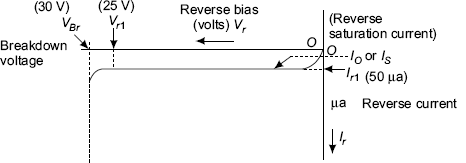
FIGURE 2.39 Reverse charateristic of semiconductor diode
Considering Vr1 of magnitude 25 volts and the corresponding reverse current Ir1 of magnitude 50 μa on the diode reverse characteristic, the value of reverse resistance Rr, which is the ratio of Vr1 and Ir1 is equal to 500 K ohms.
The diode ratings are specified in the following ways
Peak forward current.
Max anode to cathode voltage during conduction.
Max reverse voltage (peak inverse voltage). When the diode is not conducting.
Peak current specification restricting the value of filter capacitance that can be used with diode as rectifier.
Breakdown voltage rating of diodes.
where, |
CT = Transition capacitance which is voltage dependant |
|
CD = Diffusion capacitance which is current dependant. |

FIGURE 2.40 Equivalent circuit of a diode
Rf = Forward resistance of a diode in the order of ohms.
Rr = Reverse resistance of diode in the order of megaohms.
Rf can be calculated as follows.
From the equation (2.115); I = I0 ![]() for a forward biased diode
for a forward biased diode
Differentiate with respect to voltage.
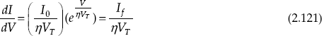
At room temperatures for a germanium diode, for a forward current of 26 mA and VT of 26 mv at room temperature of 300 degrees Kelvin.
For silicon diode (η = 2 for small currents) for a forward current of 26 mA and VT of 26 mv is ![]() 0.5 mhos.
0.5 mhos.
Forward resistance ![]() ohm for germanium device and 2 ohms for silicon device.
ohm for germanium device and 2 ohms for silicon device.
Temperature Dependence of Diode Current
Since I0 as well as VT are temperature dependent, both are taken into consideration for arriving at variation of I0 with temperature. It is already seen that n2i is temperature dependent and it is expressed as,
where VG0 is voltage numerically equivalent to band gap energy and VT is the voltage equivalent of temperature. It is of the order of 26 mv at room temperature.
In the expression for I0, the diffusion constants are involved and varying inversely with temperature. The temperature dependence of I0 can be expressed as ![]() . In the discussion up to now, the generation and recombination of electron hole pairs in the space charge region is neglected and is true for germanium but not for silicon. So, the expression for the current I has to be modified as
. In the discussion up to now, the generation and recombination of electron hole pairs in the space charge region is neglected and is true for germanium but not for silicon. So, the expression for the current I has to be modified as
![]() ; where η = 1 for large currents and η = 2 for small currents
; where η = 1 for large currents and η = 2 for small currents
Also, it is practically found that I0 is directly proportional to ni but not n2i. All these conditions can be expressed to get ![]()
Generally, this relation can be expressed as
For germanium device η = 1; m = 2; VG0 = 0.785 V and for silicon device η = 2; m = 1.5 VG = 1.21 V;
Taking logarithms on both sides for the following equation,

We know that
Using the value of VT from equation (2.124) in the equation (2.123)
Differentiating the equation (2.125) with respect to temperature T
Again, using the value of VT from equation (2.124) in (2.126)
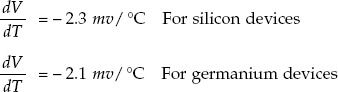
The reverse saturation current doubles for every 10°C rise in temperature both for germanium and silicon devices approximately.
Using the equations (2.118) and (2.126) it can be derived that V also is dependent on temperature and approximately varies as shown in the following expressions:
For practical design considerations it is assumed as
For both silicon and germanium devices.
The equation (2.128) suggests that ![]() decreases with increasing temperatures for the semiconductor diodes.
decreases with increasing temperatures for the semiconductor diodes.
2.15 Diode Capacitances
A P-N semiconductor diode without any bias voltage under open circuit conditions has depletion region of width W as shown in Fig. 2.31. The semiconductor diode when forward biased has a reduced depletion region width of magnitude Wf as shown in the Fig. 2.33. The semiconductor diode when reverse biased has an increased depletion region width of magnitude Wr as shown in the Fig. 2.34. This clearly shows that depletion region widths under the three situations vary with the unbiased situation to forward bias and reverse bias operations of the semiconductor diodes. So, the depletion regions about the P-N junctions are dependent on the voltage V applied to the P-N diode.
The depletion region or space charge region width on either side of the P-N junction is formed by the acceptor ions (negative immobile ions) on the P-material side and the donor ions (positive immobile ions) on the N-material side with junction voltage or contact voltage or barrier potential across the junction. The two semiconductor materials outside the depletion region containing the charges act as parallel plates and the depleted region or the transition region or the space charge region behaves as the dielectric for the junction barrier capacitances of the semiconductor devices.
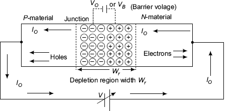
FIGURE 2.41 Semiconductor diode with reverse bias voltage V
The junction capacitances of P-N diodes present unwanted problems at high frequencies since ![]() . There are two types of capacitances:
. There are two types of capacitances:
- CT = Transition or depletion capacitance is voltage dependent under reverse biased conditions.
- CD = Diffusion capacitance is current dependent under forward biased conditions.
Space Charge Capacitance or Transition Capacitance CT
When a P-N diode is reverse biased, the reverse saturation current I0 is very much negligible and the reverse resistance is large. The contact potential or barrier voltage V0 and the depletion region width Wr about the P-N junction increase. The space charge region or the depletion region or the transition region acts as the dielectric medium and in association with the P-type and N-type materials having the acceptor ions and the donor ions, respectively behave as the parallel plates of the junction capacitance CT between the ohmic contacts. The additional feature of the capacitance is voltage variable. This feature is obtained because of depletion region width W being voltage dependent; the capacitance varies inversely as the depletion region widths. When the reverse bias voltage increases the depletion region width increases and the capacity CT decreases and vice versa.
The expression for CT is in the equation (2.129)
where, ε0 εv corresponds to dielectric constant and d corresponds to depletion region width (Wr).
A general expression for capacitance C can be obtained as follows:
where, dq = incremental charge in coulombs and dV = incremental voltage in volts.
NA is the density of acceptor ions, ND is the density of donor ions (charge densities).
Let an abrupt junction be considered in which the concentration suddenly changes from one region to the other on either side of the P-N junction, while being uniform in each region (step gradient). Placing indium against entire germanium and heating the combination to a high temperature for a short period of time can form such an abrupt junction. The indium atoms diffuse into germanium to change it a P-type on one side of the junction. It is assumed that ND >> NA. The charge density profile as a function of distance from the P-N junction is shown when NA = concentration of acceptor ions and ND = concentration of donor impurities. Also, the potential gradients are as described in the Fig. 2.42.
The field intensity (ε) profile may be readily reckoned from the illustrated voltage profile.
Since the net charge has to be conserved
When WP and WN are widths of space charge regions of P-side and N-side materials.
Since, NA << ND; Wp >> WN tends to 0.
From Poisson equation we have the relationship between potential and charge density ρ.
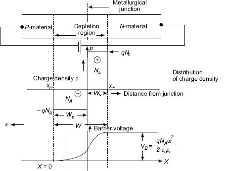
FIGURE 2.42 Charge density (ρ) and barrier potential (VB) in reverse brased P-N junction diode
where ε0 is the permittivity of the free space, εr the relative permittivity of the materials and ρ is the charge density. NA is the acceptor ion impurity concentration. q is the charge.
Integrating twice the equation (2.132)
yields,
Applying the boundary conditions in Fig. 2.42, that is at x = W, V = VB, the barrier potential (under reverse bias).
∴ Barrier voltage
The capacitance C of a capacitor can be expressed in terms of charge Q and voltage V
where, Q is the charge stored in the volume AW where A is the area of the junction and W is the depletion region width.
From equation (2.134),
Then,
![]()
Substituting the value of ![]() from the equation (2.140) in equation (2.138)
from the equation (2.140) in equation (2.138)
Similar to parallel plate capacitor
Here, in the equation (2.140); W is a function of VB.
CT can be expressed in VB by substituting for W from equation (2.134).
Then,
![]()
From the equation (2.143), it is clear that the width of the depletion region W increases with the applied reverse bias voltage VB. Substituting the value of W from equation (2.143) in the equation (2.141)
It is also known from the equation (2.141) that
![]() where permitivity of the semiconductor ɛ = ɛ0.ɛr (2.146)
where permitivity of the semiconductor ɛ = ɛ0.ɛr (2.146)
Thus, it can be finally understood that the junction capacitance, the transition capacitance CT of the P-N diode is a function of the depletion region width W and in turn varies as the square root of the reverse bias voltages (VB = V0 + VR; which is approximately equal to VR) to the diode. If the reverse bias voltage VR applied to the semiconductor diode is increased, there is a corresponding increase in the depletion region width W and the transition capacitance values get decreased proportionately. Typical value of transition capacitance CT is of the order of 20 pf. The expression for CT in the equation (2.146) also shows that the expression for the junction capacitance is similar to the expression for capacitance of a normal capacitor.
Varactor Diode The device name Varactor for the varactor diode is a shortened form of variable reactor. A reverse biased P-N junction so designed to act as a voltage variable capacitance is called a Varactor. Varactor is also known as varicap, since the capacitance of the device can be changed using a voltage. Varactor diode is symbolised in Fig. 2.43.
As the reverse bias to the diode increases, the width W of the depletion region increases and the capacitance CT decreases and vice versa.
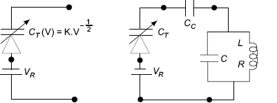
FIGURE 2.43 Varactor diode
Uses
- Voltage controlled tuning. As shown in Fig. 2.43 by varying the reverse bias VR to the diode, the capacitance shunting the tuned circuit or the tank circuit can be tuned to a range of frequencies. CC prevents the D.C. voltage entering the tank circuit. A Varactor or a set of Varactor diodes find their use as substitute for variable capacitor in the tuning stage of a radio receiver.
- Frequency modulation.
- Parametric amplifiers.
- Microwave frequency multiplication.
As explained earlier, the Varactor diode can be used for reactance control by voltages. The Fig. 2.44 shows the profile of capacitance variation with voltage for forward and reverse biased conditions. It is not linear, that is the disadvantage to some extent. The non-linearity with respect to voltage for CD is because of non-linear relationship between current and voltage of a diode.
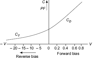
FIGURE 2.44 Capacitance variation profile under forward and reverse bias conditions
Diffusion or Storage Capacitance CD
Current dependent capacitance under forward biased constants designated by CD.
Under the assumption that NA >> ND concentration of minority carrier is a function of distance x from the P-N junction.
It becomes equal to Ipn(0) at the junction, that is, x = o
Since NA is very much greater than ND; the entire current can be considered to be of holes (i.e. injected minority carriers into the N-side region).

FIGURE 2.45 Current components contributing to diffusion capacitance CD
The charge Q is the product of A.q and dashed region of the curve as in the Fig. 2.45 as per the notation. Then,

The diffusion capacitance CD as per the definition is
From the phenomenon of diffusion it is known that
![]()
Substituting for
From the equation (2.153) in the equation (2.148); diffusion capacitance CD becomes
Since g is current dependent the diffusion capacitance CD or storage capacitance CS is a current dependent capacitance.
∵ L2P = DP.τp where τP is the mean lifetime of the charge (holes) (2.155)
The mean lifetime of the injected concentration of holes is the time constant over which period, the injected concentration falls to e–1 of its initial value. DP is the diffusion constant for holes (m2/sec). LP is the diffusion length for holes representing the distance into the semiconductor at which the injected concentration reduces to e–1 of the concentration at the P-N junction, alternately the diffusion length LP is the distance travelled by the hole before recombining with an electron, with a consequent disappearance of hole-electron pair.
Substituting the value![]() in the expression
in the expression ![]()
Then the diffusion capacitance CD = τP.g (2.156)
and
The dynamic resistance of a semiconductor diode ![]()
∴ The dynamic conductance,
Generally, CD will be of the order of 0.1 μF to 1 μF. This value of diffusion capacitance will be larger than the value of the transition capacitance CT which will be of the order 20 pf. This difference in the values of the two capacitances relates to the lowered depletion region width for forward biased P-N junction (CD is large) and the increased transition or depletion region width for the reverse biased P-N junction (CT is less than CD). So, the large value of diffusion capacitance can be a serious limitation for the use of forward biased P-N junctions in high frequency circuits. CD is directly proportional to the forward current.
For germanium diode, η = 1 and if τp = 20 μ sec and current I is 26 mA.
The value of the diffusion capacitance; CD = 20 μF.
This apparently large value of capacitance CD is not as bad in effect as to the expected, since diode forward resistance is of few ohms, and the time constant constitute of μ seconds.
In a forward biased diode, CD >> CT and CT can be neglected.
In a reverse biased diode, CT >> CD and CD can be neglected.
2.16 Zener Diodes (Voltage Regulating Diodes)
There are two types of diodes going under the name of Zener diodes,
- Zener or high field diodes with narrow junctions.
- Avalanche diodes or wide junction diodes.
The reverse bias breakdown voltage of a P-N junction can be varied by suitable or necessary concentrations of doping for P-type and N-type materials. By varying the doping concentrations, diodes with specific breakdown voltages ranging from less than one volt to several hundred volts can be manufactured. If the reverse bias applied to a P-N junction is increased to a large value, the electric field intensity increases to a very high value.
It is observed that if the transition region or the depletion region width is of the order of a few μm, voltages in the range of fraction of a volt can create very high fields. If the doping is heavy, the depletion region width decreases further and the electric field intensity becomes higher.
For instance, if v = 0.5 volt and depletion or transition width = 0.01 micron, the field intensity is
A field of such high magnitudes can directly disrupt the covalent bonds and enhance the current to high proportions. In addition, the disrupted covalent bonds producing electron-hole pairs will allow the electron-hole pair to get accelerated by these high fields and a landslide can occur. This is called avalanche multiplication. The line of demarcation between Zener and Avalanche breakdowns is very thin but yet a distinction can be made between the two.
The Zener effect (tunneling phenomenon) is considered to be a narrow junction high field phenomenon similar to field emission. As a result of very high field intensities of the order of 107 volts/m some electrons are pulled across the forbidden band gap from valence band energy levels to conduction band in diodes having narrow depletion region widths. The electron tunnels through the barrier as a wave instead of acquiring the sufficient band gap energy to cross the barrier as a particle. This phenomenon is known as the Zener effect.
On the other hand, in a wider junction due to larger mean free paths the charge carriers acquire kinetic energy, sufficient enough to disrupt the covalent bonds and start a cumulative process. This process of charge carrier multiplication is similar to secondary electron emission as in X-ray production. This is avalanche effect (impact ionisation). Paradoxically, the Zener breakdown occurs at lower voltages and the avalanche breakdown occurs at higher voltages.
When a diode is designed for a required and specific breakdown voltage, the device is called as breakdown diode. If the P-N junction of a breakdown diode for a specified breakdown voltage is well designed, the breakdown will be sharp and the current after breakdown will essentially be independent of the voltage (rated breakdown voltage). The forward and reverse characteristics of a Zener diode are shown in the Fig. 2.46.
Breakdown diodes such as Zener diodes find their applications in voltage regulators in circuits with varying inputs and also as reference voltage providing devices in regulated power supply circuits. For example, a 12 volts Zener diode used in a voltage regulator circuit holds the circuit’s output voltage at 12 volts while the input voltage to the regulator circuit varies around 12 volts.
VZ and IZK are the minimum necessary voltage and current to enter the Zener region and below this current, it cannot act as a regulating device. Above |Izk|, the voltage drop across the Zener diode is VZ and is independent of current. The maximum allowable current depends on doping and is specified by the manufacturer. It acts as a voltage regulator above IZ min and below IZ max safely.
The Zener diode draws minimum current when load current is maximum and maximum current when the load current is minimum. Zener diode regulates only when the voltage across it is at least VZ as obtained from the supply and this should always be kept in mind in designing the circuits with Zener diodes.
The heavy doping causes the current to suddenly shoot up in the close proximity of Vr as can be observed in the Fig. 2.46. Regarding the reverse characteristic below the breakdown region when Izk is crossed the current rises in negative direction virtually parallel to Y-axis. This shows no change in voltage over wide current swings, or changes as though the voltage drop across the Zener diode is constant. The Zener current and the diode resistance adjust among themselves to keep IR drop constant across the device. So, if a Zener diode were to be used in a circuit with varying voltages and currents, the voltage across a load can be maintained constant becoming immune to fluctuations in the supply voltages.
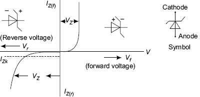
FIGURE 2.46 Forward and reverse characteristics of Zener diode
Zener Diode Circuits
In the Fig. 2.47 Vi is the input voltage and V0 is the output voltage. VZ is the Zener diode voltage drop. I is the current from the source and IZ is the current through the Zener diode. IL is the load current.
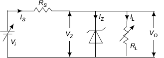
FIGURE 2.47 Voltage regulator circuit using Zener diode
As long as (Vi – I.Rs) < VZ; the output voltage V0 will be V0 = (Vi – I.Rs), since the Zener diode does not conduct and V0 = (Vi – IL.Rs). Also, IZ = 0 during non-conduction of the Zener diode.
In Zener diode regulators, when the voltage across the Zener diode is more than or equal to VZ; V0 will be clamped at VZ and V0 = VZ. As the load current increases, it is as though Zener supplies the extra current by reducing its own current. When IL is maximum IZ is minimum and when IL is minimum IZ is maximum. However, IZ minimum is necessary for the Zener diode to enter the regulation mode. The current from the supply source I is the sum of the currents IZ and IL.
The value of the resistance RS can be calculated as following:
With normal operating currents of the Zener diode; IZ is chosen as equal to 0.2.ILoad.
Power PZ dissipated in the Zener diode can be calculated as following:
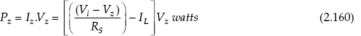
A Zener diode must be selected with larger power rating than the power dissipation rating PZ that is calculated from the equation (2.160), so that the maximum power dissipation and the temperature ratings of the device are not exceeded.
Applications of Zener Diode
- Constant voltage regulation
- Surge protection
- Clamping and clipping voltages
- Voltage reference in precision equipment such as regulated power supply circuits
- Switching operation
- For meter protection.
Advantages Smaller size, cheaper and has long life and rugged. Provides good regulation over a wider range of currents.
Drawbacks 1. Power loss associated with As for light and heavy load current and poorer efficiency. 2. Output voltage depends upon the breakdown voltage of Zener diode.
Specifications
A Zener diode is to be chosen from manufacturer’s data sheets, with the important parameter such as breakdown voltage VZ; knee breakdown voltage VZK and maximum power dissipation, and temperature coefficient. If a higher voltage cannot be provided by a single Zener diode, more number of Zener diodes is to be connected in series provided the maximum allowable current is same for all the diodes. A forward biased Zener diode can also be used as a voltage regulator but a very low Zener voltage of the order of a few tenths of a volt. But the packages are available with stacked diodes up to 1 or 2 volts. The reverse biased diodes can be used up to hundreds of volts, that is, Zener diodes are available with breakdown voltages of hundreds of volts singly or in package.
Example 1 The Avalanche diode regulates 50 volts over a range of diode current from 5 mA to 40 mA. The supply voltage is 200 volts. Calculate value of resistance R to allow voltage regulation from IL = 0 to IL max. Find IL max (Refer Fig. 2.48).
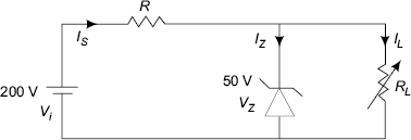
FIGURE 2.48 Zener regulator
Solution |
VZ = 50 volts and VS = 200 volts |
|
IZ max = 40 mA; occurs at IL = 0 |
![]()
If IL is maximum IZ will be minimum. So, IL max + IZ min should be maximum allowable current IS through the resistance R.
Then IL max = 40 – IZ min = 40 – 5 = 35 mA.
Example 2 A partially filtered voltage with peak ripple voltage of 25 volts with VDC = 100 volts from a rectifier is to be applied to a 50 volts Zener diode with ratings
Find the value of maximum and minimum currents through the Zener diode if IL is set at 25 mA; Rs = 3.75 KΩ. Will the Zener diode regulate? If it does not regulate, what value of Rs is needed for proper regulation to absorb fluctuation of voltage? (Refer Fig. 2.49)
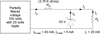
FIGURE 2.49 Zener regulation
Solution ![]()
IZ max occurs at 100 + 25 = 125 Volts
IZ min occurs at 100 − 25 = 75 Volts
Current through Rs is Is = IL + IZ max = 25 mA + 40 mA = 65 mA.
But for Rs = 3.75 KΩ; the source current Is is calculated as below:
Then, the value of Is = 20 mA and hence the Zener diode does not regulate.
So, the value if Rs is to be changed or reduced, Rs can be calculated as follows:
IZ is minimum, that is, 5 mA when VL is maximum. Then, IL = 25 mA. So, the net source current through the resistor, Is is 25 mA + 5 mA = 30 mA.
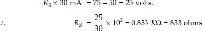
But when VL is maximum, that is, 100 + 25 = 125 volts; then Is is maximum and it is calculated as

The required IZ max is 65 mA; but this Zener diode has IZ max of 40 mA only.
So, this Zener diode cannot be used.
∴ A Zener diode with a max current (IZ max) of 65 mA should be used.
2.17 Tunnel Diode
In P-N junctions with a very narrow depletion region widths of the order of 100 Å (Angstrom units, one Å = 10−6 cm), in the materials like silicon, germanium and gallium arsenide, with high concentrations of doping of impurity elements (for example, one impurity atom doping for every 103 atoms of intrinsic semiconductor material), the device voltage versus current characteristic will be of the nature in Fig. 2.50. The electric field at the junction will be very large and the conditions become favourable for electrons on the N-material side for tunnelling through the energy barrier and spontaneously appear on the P-material side. Such devices are called tunnel diodes.
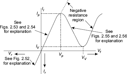
FIGURE 2.50 Voltage-current characteristic of tunnel diode
A tunnel diode is a special purpose high frequency device working on the principle of quantum mechanical tunneling. Herein, the necessity for a carrier to have energy more than the energy barrier height as in the case of normal diodes is over come. Also, the very concept of conduction is different from the normal diode conduction in that encounter between empty energy levels and filled energy levels are sufficient for conduction.
There are two practically useful properties of tunnel diode in the region between VP and VV on the device characteristic. 1) The depletion region width is very small compared to normal diodes, resulting in reduced transit times as seen from the extremely rapid transition in the diode current from its peak value IP and to the low value of current IV at the valley point and so the device is useful in applications involving signals of high frequencies up to a few gigahertz. 2) Another special feature is that it has a negative resistance over the negative region characteristic as shown on the volt-amp characteristic in Fig. 2.50, allowing it to operate as an amplifier, an oscillator and a high frequency switch.
Working Principle of Tunnel Diode
It was seen earlier that as the doping increases, the Fermi level Ef for N material moves up towards the conduction band and if the doping is heavy enough the Fermi energy level Ef can enter the conduction band and up to Ef all energy states will be filled with electrons. Similarly, for a P-material the Fermi level enters the valence band allowing empty states in the valence band. When a sandwich is made of such heavily doped P and N materials; on the P-material side empty states exist in the valence band and on the N-material side filled states appear in the conduction band. A possibility for the empty states on one side to face the filled sates on the other side can occur and conduction is possible through tunnelling of charge carriers. This phenomenon is called quantum mechanical tunnelling. Expressed differently the probability for a charge carrier having lesser energy than the barrier height may be a very low but is non-zero.
This non-zero probability may be a very low value but if concentrations are high enough; there can be enough number of carriers on the other side of the barrier with energies less than barrier height. Charge carriers may not be able to scale the height but they can bore a tunnel through the barrier and appear on the other side of the barrier. This is very much possible in reality and the process is called quantum mechanical tunnelling. P-N junctions using this property are called tunnel diodes.
For normal diode conduction, it was assumed that conduction is possible whenever electrons enter the conduction band and holes move into the valence band stated in a different way, filled states are created nearer to the conduction band in the forbidden gap and empty states are created in the forbidden gap just above the valence band. Thus, making conduction possible with very small voltages under forward bias conditions. This need not necessarily be the only method by which conduction is possible. It is sufficient if empty states and filled states encounter each other.
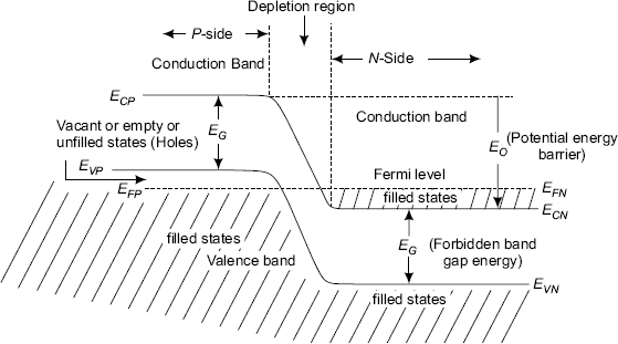
FIGURE 2.51 E.B.D. for unbiased P-N junction of tunnel diode
The Fig. 2.51 shows the Energy Band Diagram (E.B.D) of an unbiased tunnel diode. It is seen that not only the conduction band in the P-material, but also the valence band contains empty states. Similarly, in the N-material the conduction band contains filled states up to the Fermi level. But still, there can be no conduction under unbiased conditions since on either side of junction unfilled states face unfilled states and filled states face filled states.
E.B.D. for Reverse Biased Tunnel Diode
If a tunnel diode is reverse biased, the barrier height is increased by VR volts, that is, by the magnitude of the energy due to reverse bias as shown in the following Fig. 2.52. The shift in energy level EFP – EFN = qVR.
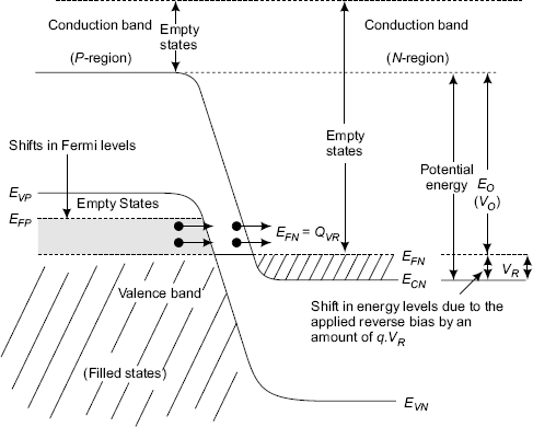
FIGURE 2.52 Energy band diagram for reverse biased function of tunnel diode
The heavily shaded area on the P-side with filled levels encounters empty states on the N-side above EFN. Thus allowing the electrons to tunnel from P-side to N-side of the diode. As the reverse bias increases, EFN goes down further and further making the thickly shaded region on the P-side larger and larger. The tunnelling current increases with reverse bias voltage Vr and is limited only by the manufacturer’s specifications. This part of the characteristic is shown in the third quadrant of Fig. 2.50 of voltage-current characteristic of tunnel diode.
Energy Band Diagrams for Forward Biased Tunnel Diode
When a tunnel diode is forward biased, the barrier height is reduced to the extent of forward bias Vf and the Fermi energy level EFN is pulled upwards relative to EFP. So that (EFN – EFP) = Q.Vf.
Then, the filled states on the N-side move up and encounter empty states on the P-side above EFP and tunnelling of electrons occur from N-side to P-side. As the forward bias increases more and more filled states on N-side face more and more empty states and the tunnelling current increases as shown in Figs. 2.52 and 2.53.
However, there is a maximum limit for this tunnelling current of value IP. (IP = Peak forward tunnelling current) as shown in Fig. 2.50 and this occurs when the maximum possible filled states face the maximum possible unfilled states on the other side (Fig. 2.54).
A further increase in the forward bias pulls EFN further up and under these circumstances, the number of the filled states encountering empty states on the other side start decreasing until the filled states on the N-side gape at the forbidden gap on the P-side and tunnelling stops and current reaches Imin as shown in Figs. 2.55 and 2.56.
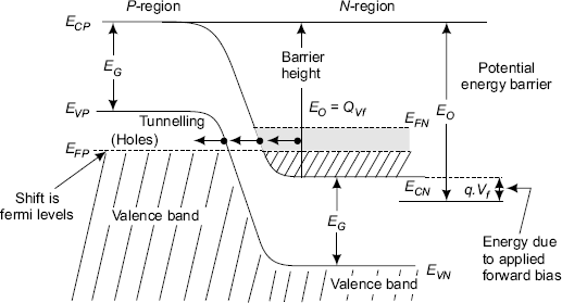
FIGURE 2.53 Energy band diagram (E.B.D.) for forword bias (forword tunnelling)
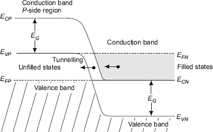
FIGURE 2.54 Maximum current for forward bias
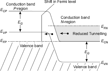
FIGURE 2.55 Further more forward bias but reduced tunnelling current
But a further increase in the forward bias beyond VV on the characteristic in the Fig. 2.50; starts normal diode conduction and the current increases with voltage. Between Imax (IP) and Imin (IV) the current decreases with increase in forward bias voltages and exhibits a negative resistance. IP : IV may be of the order of 20:1. This ratio between the maximum or peak tunnelling current IP and the valley or minimum current IV, the range of the negative resistance can be predicted. So, this ratio is useful as a figure of merit for the tunnel diode. From VForward = 0 and up to VPeak; the characteristic exhibits a positive resistance region and between Vpeak and VValley; the diode has a negative resistance and from VV and further up the Tunnel diode has again a positive resistance. VPeak to VValley voltage range predicts the voltage spread between the two positive resistance regions of the tunnel diode.
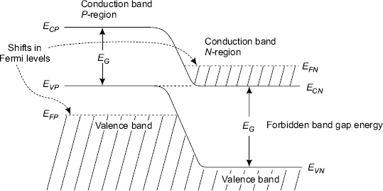
FIGURE 2.56 Forward tunnelling ends
Tunnel Diode and Its Equivalent Circuit
The symbol for tunnel diode and its equivalent circuit with typical parameters are shown in the Fig. 2.57. The tunnel diode can be represented by the above equivalent circuit, where LS corresponds to the lead inductance, RS, the equivalent series resistance Cj is the junction capacitance, R is the slope of the negative resistance region of the tunnel diode. Typical parameters are indicated on the equivalent circuit.
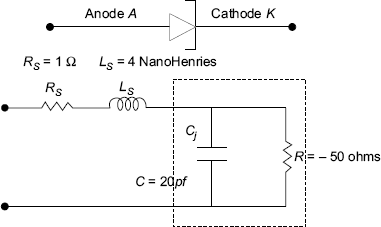
FIGURE 2.57 Tunnel diode and its equivalent circuit
The frequency of operation of a tunnel diode far exceeds the frequency calculated on the basis of depletion region width; the discrepancy can be explained as follows. The electron hitting one edge of the barrier is supposed to emit a photon, which travel at the speed of light and on arriving at the other edge of the barrier emits another electron. Thus, it is as though the photon is the particle that travels the transition region instead of the electron, which is bulkier, compared to the photon.
Applications of Tunnel Diode
- Oscillators for UHF range of the order of tens of gigahertz.
- For low access time memories.
- Pressure to current transducers.
- As mixers detectors and converters for UHF receivers.
- As a high-speed switch of the order of nanoseconds switching time.
Advantages
- Low noise figure.
- High frequency response.
- Lower dissipation.
Disadvantages
- Low voltage and current levels of operation of the device.
- Being a two terminal device, no isolation between input and outputs.
2.18 Photo Diode
A photo diode is a P-N junction which is operated under reverse bias and when exposed to light energy, the normal reverse current of the diode varies due to the generation hole-electron pairs in the junction region. As mentioned earlier, radiation affects the minority carriers more than the majority carriers. So, in reverse bias the change in current is felt much more than in forward bias. Photo conductors provide a change in conductivity proportional to the exposed optical energy. In present day electronics optical signals are also having wider range of applications with photo diodes as electronic devices.
Photo diode is an opto-electronic device that produces an electronic output (current) for a light energy input. Its applications span a wide range including sound recording on films, street light control, bar code detection on consumer products, CD reading in computer applications, fiber optic communications and as opto-isolators, which reduce coupling between input and output and a host of other applications.
It is an established fact that the reverse saturation current of a conventional diode gets doubled for every 10°C rise in temperature. But temperature rise is caused by heat, that is, thermal radiation, which is electromagnetic in nature. The difference between heat and light is only of the range of frequencies of radiation.
So, it is natural to expect the reverse saturation current to change when a diode junction is exposed to visible or invisible radiation. For instance, infra red energy in the lower invisible frequency domain and the ultra violet radiation is in the upper invisible region of the EM wave spectrum for photoelectric devices.
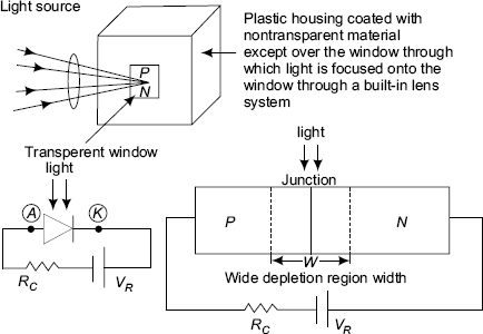
FIGURE 2.58 Construction details of photo diode
A P-N junction is housed in a clear plastic housing with inbuilt lens across an open window through which light can be focused onto the centre of the junction. If junction is exposed to radiation, minority carrier increase occurs on both the regrons about the junction. But for the window the other areas are coated with non-transparent paint.
Principle of Working
The P-N diode has depletion region width W depending on the doping on the N and P regions. When the diode junction is reverse biased, the depletion width increases and a normal reverse saturation current I0 flows. If the junction is irradiated uniformly or illuminated by photons with energy hf greater than EG, new covalent bonds break forming hole-electron pairs, thus increasing the reverse saturation current by a magnitude IL. Larger the quantum of radiation, larger changes in reverse saturation current occur. The change in reverse saturation current is almost directly proportional to the incident radiation. The current that flows in the circuit in the absence of radiation is called the dark current. The usual dark current is of the order of 10 microamps. Smaller the dark current better is the performance of the device. The signal current will be the difference between the dark current IL and the current under incidence of radiation. So, smaller the dark current, larger is the signal current from the device.
Photo Diode Characteristics
The device characteristics comprise the variation of current with reverse bias voltage for different illumination strengths that is lumens. Thus, a set of characteristics can be obtained between voltage and current one each for a specific light flux in lumens as shown in Fig. 2.59.
The expression for the current in a photo diode can be represented as follows:
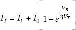

FIGURE 2.59 Photo diode characteristics
where, IT represents the total current, IL is the current due to incident illumination (optical generation of hole-electron pairs); I0 is the reverse saturation current of the diode; VB is the reverse bias voltage. In the absence of illumination IT can be seen to be just the reverse saturation current I0 for large values of reverse bias VB or simply the dark current which is of the order of 10 microamperes. The incident illumination produces excess electron-hole pairs proportional to illumination as explained earlier.
In the absence of radiation or illumination is cut-off or zero illumination, the voltage across RL is almost negligible if the dark current is small (dark current is of the order of 10 microamps). When light falls on the window of the photo diode, the current increases in proportion to the incident light energy (when hf is greater than EG) and a voltage is developed across RL, which constitutes the signal. Optical signals can thus generate a proportionate voltage output and a photo diode can serve as an opto-electronic converter. For instance, 0s and 1s (in the form of no light and light) can produce lower and higher voltages corresponding to binary digits.
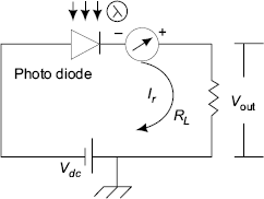
FIGURE 2.60 Application circuit
2.19 Rectifier Circuits
All electronic devices require carrier movement caused by discrete positive and negative potentials. Also, D.C. is used as the supply voltage for most amplifiers and electronic gadgets. These D.C. sources may be battery for portable equipment but are very expensive for heavy use, and involve other problems like leakage and periodic charging. An alternative is to convert the cheaply available A.C. from power lines to D.C. and such converters are called rectifiers. The principle of operation essentially is to convert A.C. into unidirectional voltages and currents using polarity sensitive switches, that is, diodes, and others.
The half-wave rectifier circuit has a step down transformer, a semiconductor diode, a variable load resistor RL, and a capacitor C as connected in the Fig. 2.61.
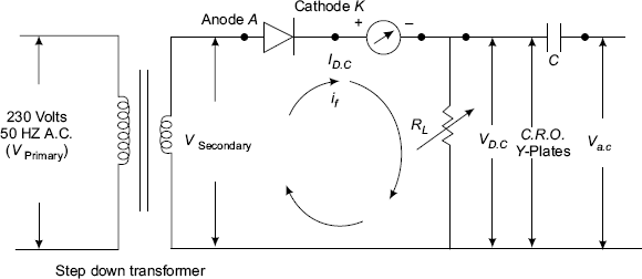
FIGURE 2.61 Half-wave rectifier circuit
The step down transformer reduces the power line A.C. voltage at 230 volts 50 Hz to the required level depending on the application, for example, 6 volts or 9 volts and so on. The diode conducts only when the anode is positive. Thus, in a half-wave rectifier diode conducts only during one half-cycle. So, the load current is varying D.C. containing D.C. average value and an A.C. component (unwanted signal component) called the ripple voltage. The capacitor blocks the D.C. and allows the ripple to be measured and thus obtaining the estimate of the unwanted A.C. with respect to the D.C. called the ripple factor.
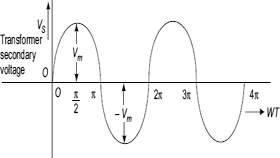
FIGURE 2.62 Transformer secondary voltage VS
Transformer secondary voltage: Vs = Vm sin ωt. (Input voltage to the diode)
During the interval 0 to π (half-cycle) of the supply voltage, the anode (P-material) of the semiconductor diode is positive and hence, the diode is forward biased.
Forward current If flows through the circuit.
Since, the forward resistance rf of the semiconductor diode and the transformer secondary winding resistance rS are generally small in comparison with load resistance RL.
Thus, the current If flows through RL. There is potential Vout developed across RL.
During π to 2π of the secondary voltage VS the semiconductor diode is under reverse bias condition. Reverse current Ir flows through the circuit but it is of practically negligible value. Ir ≅ 0. So, the voltage developed across the diode under reverse bias should be less than breakdown voltage (the maximum voltage across the diode has to withstand) or safe voltage under reverse bias (without breakdown of the diode) is known as Peak Inverse Voltage (PIV) of the diode.
The voltage across RL = Ir × RL ≅ 0.
Thus, alternating secondary voltage Vs acting as input voltage Vin to the semiconductor diode develops unidirectional voltage wave form across RL. Such a circuit is known as a rectifier. Some assumptions made in the analysis:
The semiconductor diode is assumed to have negligibly small forward resistance rf so that the voltage drop across the diode during conduction is zero.
During the reverse bias period of the semiconductor diode, the reverse saturation current Ir approximates to zero.
Transformer resistance and leakage reactance are neglected for the present to simplify the procedure.
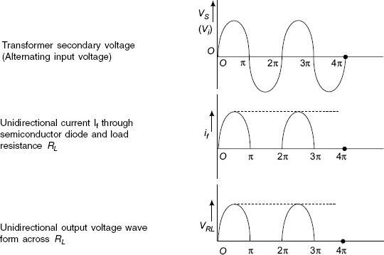
FIGURE 2.63 Voltage waveforms in the circuit that can be observed on the CRO
The cut-in voltage Vγ of a silicon diode is 0.7 volts and that for a germanium diode is 0.3 volts. Since, the normal secondary input voltages to diodes are large in comparison with Vγ; Vγ is taken to be zero.
As evident from the signal wave form of if, the D.C. component or the average value of the current Idc is calculated as following:
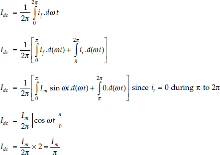
If Im = Vm /RL is substituted in the above expression
The D.C. component Idc can be measured by the D.C. ammeter in series with the load RL in the rectifier circuit.
D.C. voltage across RL is Vdc = Idc × RL.
As rf is considered to be approximately zero,

Vdc is the average value of the positive half-cycle of Vs or Vin.
The A.C. power Pa.c supplied to the circuit
The effective or rms value of current (Irms)
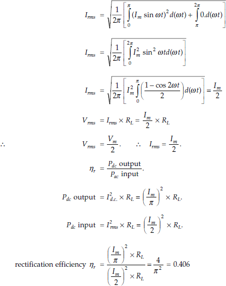
The efficiency of rectification ηr is defined as the ratio of D.C. output power (Pd.c output), across the RL to the A.C. input power (Pa.c input).
For the discussed half-wave rectifier circuit, rectification efficiency is approximately equal to 40%. This is of no consequence in normal low power circuits but is to be considered in high power rectifiers. In this calculation the effect of Rf are ignored. If they are taken into consideration then η will be less and varies with load. The maximum efficiency %η we can get is 40.6%.
Ripple frequency of the half-wave rectifier is the number of half sinusoids per second in the output voltage wave form observed across the load resistance RL using a CRO. Since, for one cycle of A.C. input signal wave form, one half sinusoid is observed across RL; for supply frequency fS of 50 Hz; 50 half sinusoids can be observed per second. So, the ripple frequency fs becomes 50.
Ripple Factor (γ)
By definition
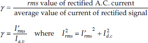
where, Irms = rms value of A.C. signal
I’rms = rms value of rectified a.c signal and represents the unwanted A.C. component relative to the desired D.C. under no load condition as measured using a multimeter or a CRO.
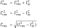
ripple factor

Voltage Regulation
The fractional variation of D.C. output voltage with respect to no load D.C. voltage with variations in D.C. load current as a percentage (%) is defined as regulation.
No load voltage V no load of the half-wave rectifier circuit in Fig. 2.64 can be measured using a multimeter or a cathode ray oscilloscope.
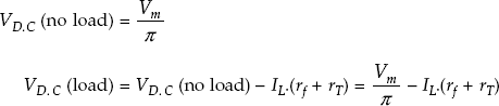
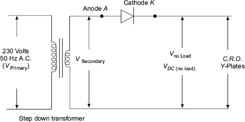
FIGURE 2.64 Half-wave rectifier circuit (no load)
where, rs or rT is the secondary winding resistance of the transformer and rf is the forward resistance of the diode.
For different values of load resistance RL, that is, different values of load current IL; the load voltages VLoad are measured using a CRO in the circuit shown in Fig. 2.65.
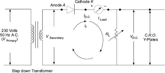
FIGURE 2.65 Half-wave rectifier circuit (voltage regulation determination)
Regulation values are calculated for different values of IL using the above equation. The graph between load current IL and the regulation makes us to understand the performance of the power supply
For a good power supply circuit, the quantity | Vno load – Vload | should be zero or constant making the regulation zero or independent of load. The output voltage should be independent of load current at least over a desired range of load current for ideal voltage regulation.
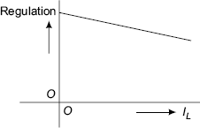
FIGURE 2.66 Voltage regulation curve (w.r.t. load current)
Vdc and Vac are measured at nominal I L for predicting the value of ripple factor. The ripple factor, as discussed earlier, is the ratio of Va.c. to Vd.c. as measured from the circuit (Fig. 2.67). The ripple factor varies with I L. The capacitor blocks D.C. and allows the A.C. component or ripple voltage to be measured. Thus, the half-wave rectifier circuit is the basic building block for understanding and building the other rectifier circuits.
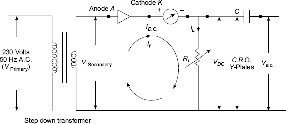
FIGURE 2.67 Half-wave rectifier circuit to measure ripple factor
Full Wave Rectifier Circuit
The full wave rectifier circuit consists of a mains transformer, two semiconductor diodes D1 and D2; load resistance RL and a capacitor C as connected in the Fig. 2.68. The secondary winding of the transformer has a centre–tap and the two voltages VS1 and VS2 are 180° out of phase and equal in magnitude.
During the interval 0 to π of the secondary input voltages VS1 and VS2; semiconductor diode D1 is forward biased, If flows through RL and hence develops output voltage Vout = If × RL. At the same time semiconductor diode D2 is reverse biased. Ir2 ≅ 0 flows through RL.
During π to 2 π of the secondary voltages Vs1 and Vs2; the polarities of the voltages across the secondary winding are such that semiconductor diode D2 is forward biased and D1 is reverse biased. If2 flows through RL and develops voltage Vout across the load resistance, RL. Vout = If2 × RL. Since the semiconductor diode D1 is reverse biased, the reverse current Ir1 ≅ 0 flows through RL.
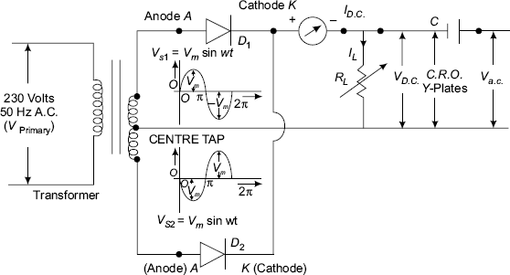
FIGURE 2.68 Full-wave rectifier circuit

FIGURE 2.69 Transformer secondary voltages
From the output voltage wave forms, Vout across the load RL, we find that current through the load R L exists during both half-cycles of the A.C. input cycles. Hence, increased D.C. power output supplies can be obtained.
It is also evident from the full wave rectifier circuit that it has two half-wave rectifier circuits with common load. These are connected in such a way that conduction takes place through two diodes in alternate half-cycles and current through the load is the sum of the two currents If1, and If2 as indicated by arrows. Thus, the output voltage wave form contains two half sinusoids in the two half-cycles of the A.C. input signal in the first quadrant only.
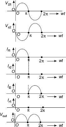
FIGURE 2.70 Wave forms of full-wave rectifier circuit
Full-wave rectifier circuit is seen to behave as two half-wave rectifier circuits with common load RL. Each diode D1 or D2 operates under identical conditions, and the load currents get combined in the common load RL.
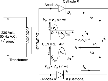
FIGURE 2.71 Full-wave rectifier circuit

FIGURE 2.72 Output wave forms in full wave rectifier circuits
Average value of the half sinusoids shown in Fig. 2.72, Idc is as following:

Output D.C. voltage VDC = ![]()
Idc and Vdc values for a full wave rectifier circuit are twice that for half-wave rectifier circuit D.C. output voltage Vdc for full wave connection is twice that of half-wave rectifier circuit.
From the above two equations for Idc and Vdc,
The rms value of load current can be obtained as in H.W.R. expressions Irms = ![]()
The rms value of load voltage Vrms can be obtained as in H.W.R. expressions
Total A.C. power input
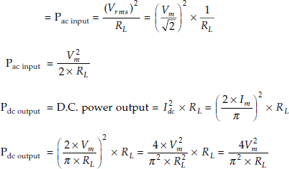
Efficiency of rectification
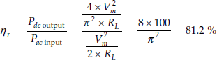
Rectification efficiency of full wave rectifier circuit is twice that for half-wave rectifier circuit. From the equations,
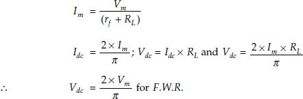
From the above expression, the D.C. output voltage Vdc varies with current.
Ripple factor:

Significance of ripple factor For example, for a full wave rectifier, we will get 0.48 volts of unwanted A.C. for every one volt of wanted D.C.; whereas for a half-wave rectifier for every one volt of wanted D.C. we get 1.21 volts of unwanted A.C. component. Filtering circuits reduces this ripple voltage.
Peak Inverse Voltage Each diode in the F.W.R. circuit, during reverse bias condition has to withstand a maximum voltage, 2Vm that exists across the total secondary winding, of the transformer. This maximum voltage, 2Vm across each diode under reverse bias condition is known as peak inverse voltage.
So, in F.W.R. rectifier circuit PIV = 2Vm, each diode has to be selected with its breakdown voltage greater than 2Vm.
2.20 Bridge Rectifiers
Bridge rectifier is a full wave rectifier circuit without the requirement of a centre tap on the secondary winding of the transformer. In a full wave rectifier a centre-tapped transformer feeds two diodes and conduction takes place during each half-cycle through one diode. The maximum no load voltage is ![]() , where Vm is the voltage across one section of the secondary winding of the transformer. The full voltage across the transformer secondary can be connected to a bridge there by using the full transformer voltage thus making the no load maximum voltage
, where Vm is the voltage across one section of the secondary winding of the transformer. The full voltage across the transformer secondary can be connected to a bridge there by using the full transformer voltage thus making the no load maximum voltage ![]() where 2Vm is the voltage across the full secondary, that is, 2V m is the supply voltage to the bridge rectifier; thus giving twice the voltage compared to the normal full wave rectifier.
where 2Vm is the voltage across the full secondary, that is, 2V m is the supply voltage to the bridge rectifier; thus giving twice the voltage compared to the normal full wave rectifier.

FIGURE 2.73 Bridge rectifier circuit
When the upper terminal A of the transformer secondary is positive during the half-cycle, 0 to π of the secondary voltage, diodes D2 and D4 conduct (diodes D3 and D1 are reverse biased) in series developing a D.C. voltage across the load RL with terminal C positive.
On the other hand, during π to 2π interval of the transformer secondary voltage, when the terminal B is positive diodes D3 and D1 conduct in series (diodes D4 and D2 are reverse biased) and the current flowing through RL in the same direction making the terminal C of the load positive again. Thus, the two currents flow through the load resistance in the same direction to increase the output D.C. voltage. The secondary current is present during both halves of the secondary voltage, thus the transformer is fully utilised.
The advantage of this configuration is that it gives twice as much D.C. as compared to full wave rectifier circuit for the same secondary of the transformer. Further, with reduced size of the semiconductor diodes, the use of four diodes in the bridge rectifier circuit has become popular as a package. The ripple factor and regulation are same as that of full wave rectifier,
The peak inverse voltage (PIV) is the same as that of half-wave rectifier, that is, Vm across each diode. Disadvantages are 1) Since the two diodes are in series during conduction, twice the voltage drop reduces the output voltage. 2) It needs four diodes.
Full Wave Doubler
In the full wave voltage doubler circuit the diodes are connected to the same voltage source Vm but in the opposite direction.
The circuit in the Fig. 2.74 is a full wave voltage doubler. When the upper terminal A of the transformer secondary is positive, the semiconductor diode D1 conducts and charges the capacitor C1 to the peak voltage V m of the input voltage. On the other hand, when the lower terminal B of the transformer secondary is positive the diode D2 conducts and charges the capacitor C2 to the full input voltage V m as shown in the Fig. 2.74. Meanwhile, the charge acquired by C1 is retained, since the voltage across the diode D1 is due to the reverse bias. Hence, the voltages across both the capacitors are with such polarities that the D.C. output voltage, VDC is equal to twice the peak input voltage. Therefore, VDC = 2 Vm under no load conditions.
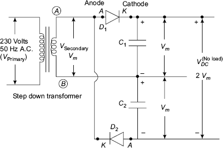
FIGURE 2.74 Full wave voltage doubler
The net output voltage is 2Vm under no load conditions. When loaded, the capacitor discharges depending on RL. The output voltage falls quickly as the time constant decreases with decrease in RL, that is, increased load current. For fixed light loads, the output voltage is almost twice as that can be obtained for a full wave rectifier with centre-tapped transformer and half-winding. The capacitors need withstand Vm and the diodes have to withstand 2Vm.
2.21 Filters
It is observed that the output of a rectifier is a pulsating D.C. consisting of a D.C. component and superimposed ripple (A.C. content). In most cases a pure D.C. or a D.C. with tolerable ripple is needed. The filter design becomes complicated and costly if the ripple has to approach zero value. In most practical cases, the requirements are not that critical. A way to eliminate or reduce the ripple to the required level is to use a filter.
Since the reactive elements like inductors and capacitors respond to D.C. and A.C. differently, these can be used to reduce A.C. content relative to D.C. in the rectified output voltage. Filtering process is achieved using low pass filters which are suitably connected capacitors, inductors and a combination of them such as shunt capacitor filter, choke input filter, L-Section filter and p-section filters depending on the purity of D.C. required or the level of ripple content that can be of no problem in a particular application. Thus, a power supply filter reduces the magnitudes of all the alternating components or the ripple content in the rectified output wave forms and passes the D.C. content. Ripple factor is used as a measure of effective functioning of a filter circuit. Ultimately, for good filter circuits ripple factor should be as small as possible indicating the reduction of A.C. component in the filtering process.
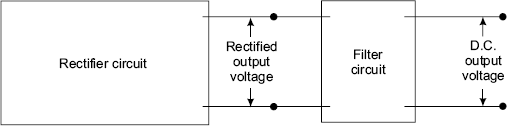
FIGURE 2.75 Combination of rectifier and filter circuits for D.C. source
Inductor Filter
An inductor opposes changes in current and thus the pulsations, for example, the ripple content in the rectified output voltage fed to the filter circuit can be smoothened out by keeping a series inductance in the filter circuit as shown in the following Fig. 2.76A.
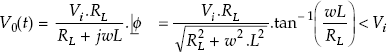
As the magnitude of inductance L becomes more and more, the output ripple becomes lesser and lesser and the conducting angle increases, assuming that choke input filter is supplied with the output of a half-wave rectifier circuit as shown in Fig. 2.76.
For a full wave rectifier circuit, the ripple frequency is 2f S and the pulsating output V0(t) can be considered to contain

FIGURE 2.76A Inductor filter
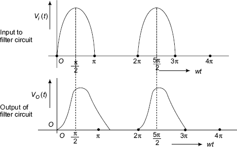
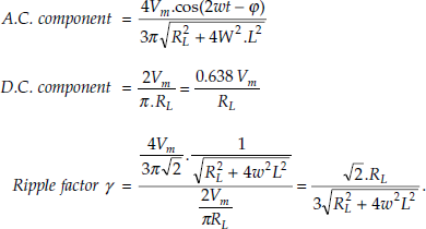
If (4w2.L2/RL2) is much greater than unity,
Ripple factor γ = ![]()
Therefore, ripple factor will be small for low values of load resistance RL. Thus for high values of load current and larger values of inductance (L), the ripple factor will be less.
2.22 Capacitor Filter Circuits
Half-wave Rectifier Circuit with Capacitor Filter
This simple and usual filter circuit uses a capacitor connected in parallel with the load resistance RL. A capacitor connected in shunt across the load resistance provides a bypass path for A.C. component or ripple content present in the output voltage of the rectifier circuit and the ripple gets reduced.
Physically, the capacitor C gets charged to the peak value of the rectified voltage Vm during the period of conduction of the diode and discharge through RL (as the diode is reverse biased at this juncture and offers infinite reverse resistance and so does not provide any path for capacitor to discharge any charge through the diode) after the rectified voltage decreases from its peak value in a time period of the time constant CRL. If CRL is much larger than T (the time period of the input voltage), the ripple output voltage can be approximated to be a triangular wave superimposed on the D.C. Larger the value of the capacitance C, greater is the reduction in ripple. The performance of the capacitor filter circuit is clear from the wave forms shown in the Fig. 2.78.
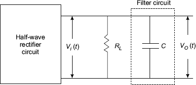
FIGURE 2.77 Half-rectifier circuit with capacitor filter

FIGURE 2.78 Effect of shunt capacitor filter on rectifier output wave form for half wave rectifier
Full-wave Rectifier Circuit with Capacitor Filter
From the wave forms in the Fig. 2.78, it is seen that the shunt capacitor filter used with half-wave rectifier prolongs the time period during which the current passes through the load resistance and the ripple is very much reduced. This situation is further improved towards the reduction of ripple level V r when the shunt capacitor filter is used with a full wave rectifier circuit as seen in the following wave form diagrams in the Fig. 2.80.
In the circuit of Fig. 2.79, capacitor filter uses the output voltage of a rectified output V i (t) from a full wave rectifier circuit.
The approximate model wave forms across the shunt capacitor filter with a full wave rectifier circuit are shown in the Fig. 2.80. The charging time T1 is much less than the discharge time T2. The total time T1 + T2 is approximately equal to T2 = (1/2 f); where f is the Power line frequency.
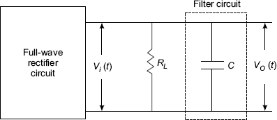
FIGURE 2.79 Full wave rectifier circuit with capacitor filter
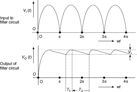
FIGURE 2.80 Full wave rectifier with shunt capacitor filter output voltage wave forms
![]() where Vr is the peak to peak amplitude of the triangular wave. The rms value of the triangular wave is known to be
where Vr is the peak to peak amplitude of the triangular wave. The rms value of the triangular wave is known to be ![]()
But Vr is the peak-to-peak amplitude of the A.C. voltage across the capacitor obtained by the charging of the capacitance by the current IDC in a time T.
From this expression for the ripple factor, it can be inferred that with increasing values of the capacitance C and RL; the ripple gets reduced. That is for smaller values of IDC and large values of capacitance, ripple content will be less and smoother will be the output wave form.
∵ Ripple voltage
The ripple factor
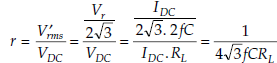
L-section Filter or Choke Input Filter or L-filter
The benefits and merits of both inductance L and capacitance C can be combined in a L-section filter or the so-called L-C filter or choke input filter. Inductor is added prior to and in series with the capacitor filter as shown in Fig. 2.81.
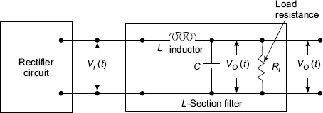
FIGURE 2.81 L-section filter circuit
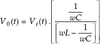
The series inductor L drops A.C. which is further bypassed by capacitance C and the ripple gets reduced by a factor

and contributes to the filtering action.
The final expression for ripple factor of the L-C filter is
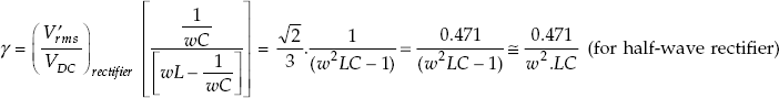
For a full wave rectifier since the ripple frequency is 2f the above expression for ripple factor gets modified to
Here, the ripple factor is independent of the load currents. Hence, L-section filter is used in applications having wide variations of load currents.
Regulation characteristic graph between VDC and IDC is called the regulation characteristic. The Fig. 2.82 shows the voltage regulation characteristics of L-section filter and capacitor input filter circuits.

FIGURE 2.82 Regulation characteristic
π-Section Filter
A combination of capacitor input and L-section filters is the π-section filter as shown in Fig. 2.82. The π-section filter circuit is most popular.

FIGURE 2.83 π-section filter circuit
The ripple is very much reduced by the double filtering action.
Regulation Characteristic Fig. 2.84 shows the regulation characteristics of various types of filters.
For L-section or π - section filters no load D.C. voltage
As the current increases for an L-section filter the voltage quickly drops and then changes more smoothly, since the inductance L smoothens the varying current. Also, the ripple is less dependent on the load current. This L-section filter circuit is useful for large fluctuating loads. On the other hand, a π - section filter has always a relatively high D.C. voltage up to IL0 ; the optimal load current. Thus, π - section filter circuit is preferable for light (small) fixed load currents, since it provides high D.C. relatively.
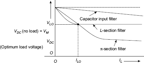
FIGURE 2.84 Regulation characteristics
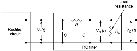
FIGURE 2.85 π-section filter circuit using RC elements
For low current circuits, a resistor replaces the inductor element. This R-C filter circuit is useful only if IR drop across the resistor is not much and also if regulation is not of much importance in the application especially for low voltage supplies like the transistor regulated power supplies. The π - section filter is preferable to single capacitor input filter circuit.
Questions for Practice (Semiconductor Diode)
- Draw the diagram showing the electronic configuration of germanium atom to show that germanium (semiconductor) is a tetravalent material.
- Draw the diagram showing the electronic configuration of silicon atom to show that silicon (semiconductor) is a tetravalent material.
- Draw the diagrams giving energy band structure of (a) conductor (b) semiconductor and (c) insulator.
- Mention the group of elements to which the silicon and germanium semiconductors belong.
- Mention the two types of intrinsic or pure semiconductors used for the fabrication of transistors.
- Mention the necessity of obtaining P-type and N-type semiconductors.
- Mention the two main types of extrinsic semiconductors used in the fabrication of semiconductor devices.
- What is the medium of flow for the charge carriers in semiconductor devices?
- Doping trivalent material atoms to intrinsic semiconductor provides _____ majority carrier concentration and _____ minority carrier concentration.
- Doping pentavalent material atoms to intrinsic semiconductor provides _____ majority carrier concentration and _____ minority carrier concentration.
- In an intrinsic semiconductor the mobility of electrons in the conduction band is _____ than the mobility of holes in the valance band.
- Doping _____ the conductivity of extrinsic semiconductor materials.
- Hole mobility is less since it moves _____ only.
- Define lifetime of charge carriers in semiconductors.
- Mention the main reason for using silicon semiconductor devices over germanium devices to work at high temperatures.
- Define hole current and deficit conduction in P-type semiconductors.
- Define excess conduction in N-type semiconductors.
- List donor impurity atoms and acceptor impurity atoms.
- Distinguish between drift and diffusion currents in semiconductors.
- Discuss the formation of contact potential in open circuited P-N junction.
- What do you understand by transition region or space charge region or depletion region about P-N junction in P-N diodes?
- State Einstein relationship.
- The mobility of the hole is less than that of the electron. Explain.
- Define the mean lifetime of a charge carrier.
- Define diffusion length.
- In a semiconductor material, the injected minority carriers fall exponentially with the distance and the time. Yes or No?
- State Hall effect phenomenon.
- What are the applications of Hall effect?
- Mention the method of determination of the type of semiconductor material based on Hall effect.
- Mention the expression for Hall coefficient.
- Define Fermi level and explain its significance in the energy band diagrams.
- During Zener effect, mention whether the charge moves as a particle or a wave.
- Fermi level shifts towards _____ in P-type semiconductor.
- Mention the significance of forbidden band gap energy with reference to the difference in cut-in voltages for silicon and germanium diode working under forward bias conditions and also mention the reason for silicon devices to work at higher temperatures when compared to germanium devices.
- Fermi level shifts towards _____ in N-type semiconductor.
- Recombination of electrons with holes in a semiconductor occurs over a time as well as _____.
- Mention the expression for current density J in N-type and P-type semiconductors.
- Draw the charge profile diagrams of P-type and N-type semiconductor materials.
- In a P-N diode with a junction draw the charge profiles diagrams and mention the reason for diffusion current through the device.
- Mention the source for potential barrier concentration or charge gradient VB across a P-N junction of a semiconductor diode and mention its significance.
- Mention the reasons for the formation of depletion region about the junction of a P-N diode.
- Mention the expression for VB (contact potential or barrier voltage) in terms of concentration of dopant atoms for a P-N junction diode.
- VB decreases by _____ mV for every °K increase of temperature.
- Mention the expression for diffusion current density in P-type semiconductor.
- Mention the importance of barrier voltage or built in voltage VB in the working of a semiconductor diode.
- Mention the expression for drift current in P-type semiconductor diode.
- Draw the circuit diagram showing the method of obtaining the forward characteristic of a semiconductor diode.
- Draw the Vf versus If characteristic (forward characteristic) of a semiconductor.
- Explain the factor that is responsible for the diode to function as a closed switch.
- Mention the diode forward current equation.
- Mention the magnitudes of cut-in voltages Vγ for silicon and germanium diodes.
- Draw the circuit diagram showing the method of obtaining the reverse characteristic of a semiconductor diode.
- Draw the Vr versus Ir characteristics (reverse characteristic) of a semiconductor diode Explain the feature that is responsible for the diode to function as an open switch.
- Mention the constraint on the magnitude of reverse bias for the diode to act as an open switch.
- Find the change in voltage required to keep constant 10 mA of diode current when the temperature rises by 10 °K for a germanium diode from room temperature.
- Give the equivalent circuit of a forward biased diode.
- Differentiate between dynamic and static resistance of a diode.
- The current through silicon diode, I f = 60 mA for a forward bias of Vf =0.6 Volts. Calculate the static resistance of the diode.
- The reverse saturation current I s at T = 300 °K of a P-N junction germanium diode is 5 microamps, calculate the forward bias voltage Vf to be applied across the junction to obtain a forward current I f of 50 mA.
- Mention the reasons for sudden increase in reverse current I r of a P-N diode when reverse bias Vr is equal to breakdown voltage Vbr of the diode.
- Explain Zener effect and explain how it is similar to field emission.
- Explain Avalanche effect and how it is similar to secondary electron emission.
- Define transition capacitance of a semiconductor diode and mention the expression for transition capacitance.
- Define diffusion capacitance of a semiconductor diode and mention the expression for diffusion capacitance.
- The transition capacitance of a diode is 20 pf. εr = 16; A = 1 square mm; εo = 8.854 pf/m given that Vγ = KW2; where K = 0.28 v/m2; find the voltage Vγ to be applied to achieve the said value of capacitance.
- If τ = 10 μsec; I = 78 mA; find Cd for a silicon diode with η = 2 and VT = 26 mv.
- Mention the reasons for a semiconductor diode to act as an open switch for a diode with reverse bias and as a closed switch with forward bias.
- Zener breakdown occurs at a _____ voltage than the Avalanche breakdown since the former is a field effect phenomenon.
- Draw diagram of a simple voltage regulator circuit using Zener diode.
- A _____ biased P-N diode is called a _____ when it is optically energised.
- Natural current source is a _____.
- Tunnelling occurs whenever allowable empty states encounter _____ or ______.
- Tunnel diode has the disadvantage in that it is _____ terminal device.
- What is tunnelling phenomenon?
- What are the applications of tunnel diode?
- Draw the tunnel diode characteristic with salient features on it.
- Differentiate between Avalanche breakdown and Zener breakdown.
- Mention the function of a rectifier circuit.
- Draw the circuit diagrams of a half-wave rectifier.
- Mention the theoretical maximum value of rectification efficiency of a H.W.R.
- Mention the theoretical maximum value of rectification efficiency of a F.W.R.
- Comment on the ripple factors of half-wave and full wave rectifier circuits with reference to the ripple content in the rectified voltages.
- Define utilisation factor of a transformer.
- Define form factor.
- If the output voltage VDC of a bridge rectifier circuit is 12 volts, calculate the peak inverse voltage rating of each diode.
- Calculate the value of Vdc for a half-wave rectifier circuit, if Vrms = 30volts, across the secondary winding of the mains power transformer.
- Mention the expression for the ripple factor of a half-wave rectifier and give the typical value.
- Draw the output wave form of a half-wave rectifier circuit assuming the A.C. input of 50 Hz.
- Define ripple frequency for F.W.R. and H.W.R. circuits.
- For a rectifier circuit, mention the expression for regulation.
- Draw the full wave rectifier circuit with centre-tapped secondary power transformer.
- Calculate the magnitude of Vdc; if the voltage applied to each diode is 30Vrms.
- Calculate the magnitude of ripple factor for given following set of observations of Vac = 24.2 volts and Vdc = 20 volts. Identify the type of rectifier circuit based on the knowledge of theoretical values of ripple factors for H.W.R. and F.W.R. circuits.
- Calculate the magnitude of ripple factor for given following set of observations of Vac = 24 volts and Vdc = 50 volts? Identify the type of rectifier circuit based on the knowledge of theoretical values of ripple factors for H.W.R and F.W.R circuits.
- Mention the magnitude of ripple frequency of a rectifier circuit, if the output wave form of the observed rectifier contains 50 half sinusoids per second and the A.C. supply frequency is 50 Hz. Also identify the type of rectifier circuit.
- Show the nature of output wave forms for a half-wave and F.W.R. circuits for one cycle of A.C. input signal with supply frequency of 50 Hz.
- If Vm = 24.2 volts for an F.W.R. circuits, mention the magnitude of PIV (peak inverse voltage) rating of each diode and what does it demand on diode specifications?
- Given Rf (forward resistance of a semiconductor diode) is 100 ohms and the ripple factor is 0.048; find the value of capacitor for a capacitor input filter.
- No load output voltage for a rectifier with L-section filter is 2Vm/π. Mention whether it is used with H.W.R. or an F.W.R. circuit.
- Draw the circuit of a bridge rectifier and compare its performance with a full wave rectifier circuit using a mains transformer with centre-tapped secondary winding.
- Draw the regulation curve of a rectifier with L-section filter circuit.
- Draw the regulation characteristics for L-section filter circuit, capacitor input filter circuit and π-section filter circuit and compare their performances.
- Draw the F.W.R. circuit with shunt capacitor filter and draw typical output wave form.
- Discuss the nature of output wave forms across the shunt capacitor to load resistance RL, when used as a filter with half-wave and full wave rectifier circuits.
- Mention the functioning of filter circuits in D.C. power supply circuits.
- Mention the effect of ripple in the output of rectifier circuits.
- Mention the parameters that cause for fluctuations in output voltage of a regulated power supply circuit.
- What do you understand by voltage regulation?
- Draw the Zener diode characteristics.
- Draw the simple voltage regulator circuit using a Zener diode.
- Explain Zener effect.
- Compare the doping levels of Zener diode and normal diodes.
- Mention the various factors that are to be considered for selecting Zener diodes in voltage regulator circuits.
- Mention the name of the constant voltage across a Zener diode after breakdown.
- Calculate the factor by which the reverse saturation current of a germanium diode is multiplied when the temperature is increased from 25°C to 80°C.
- Draw the energy band diagram of tunnel diode.
- Draw the V-I characteristics of tunnel diode.
- Mention the principle of working of a varactor diode.
- Mention a few important applications of varactor diodes.
- Mention the relation between the junction capacitance and the reverse bias voltage applied to a varactor diode.
- Mention the relation between rms voltage Vr and IDC for a π-section filter.
- Mention the device name that exhibits variable junction capacitance when reverse bias voltage is applied to a diode.
- Mention the main disadvantage of a tunnel diode.
- Draw the tunnel diode characteristic and mark the negative resistance region and positive resistance regions.
- Mention the main applications of tunnel diode.
- Tunnelling of charge carriers occurs in a tunnel diode whenever allowable empty states encounter _____ or _____.
- Draw the equivalent circuit of a tunnel diode.
- Explain the significance of the ratio of peak current to valley currents on the tunnel diode curve and its relation to the figure of merit of tunnel diodes. Explain its significance as the device to operate as a high speed switch.
- Mention the order of depletion region width of a tunnel diode when compared to normal diode depletion region widths.
- Mention the expression for total current IT of a photo diode.
- Draw the photo diode characteristics and mark the dark current region and the current region due to light energy.
- Define the situation of dark current of a photo diode.
- Draw the main structural details of a photo diode.
- Mention a few important applications of photo diode.
Solved Examples
Example 1 In a half-wave rectifier circuit,
Vbreakdown = 50 volts.
Calculate the values of Im, Irms, IDC; D.C. power output, A.C. power input; r; ηR.
Solution
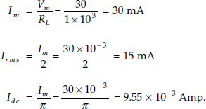
D.C. power output = Idc2 × RL = (9.55 × 10⁻³)2 × 1 × 103.
Pdc output = 9.552 × 10−3 = 91.2 mW.

Example 2 The transformer of a half-wave rectifier has a secondary voltage of 30 volts (Vrms) at 50 Hz with winding resistance rs of 10 ohms. The semiconductor diode in the circuit has a forward resistance rf of 10 ohms.
Determine
- No load D.C. voltage.
- D.C. output voltage when the load current IL = 25 mA.
- Percentage regulation at this load current.
- Ripple voltage across the load, ripple frequency fs and ripple factor r.
- D.C. power output.
- A.C. power input.
- Power conversion efficiency.
- Peak inverse voltage, the semiconductor diode has to withstand.
Solution
- No load D.C. voltage:
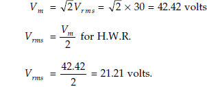
No load D.C. voltage,
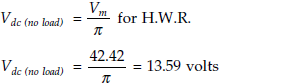
- Considering the voltage drops across rf and rs due to the flow of load current IL = 25 mA through them.
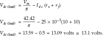
- Percentage regulation at this load
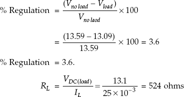
- Ripple factor r =
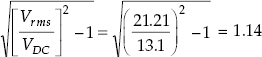
Ripple voltage across load = ripple factor × VDC(load) = 1.14 × 13.1 ≅ 16 volts.
Ripple frequency = fs = 50 Hz.
- D.C. power output
PDC = Idc2 × RL = (25 × 10−3)2 × 524 = 327.5 m watts
- A.C. power input
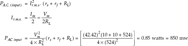
- Rectification %
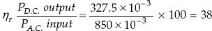
- Peak Inverse Voltage = 42.42 volts (PIV is equal to the max voltage across secondary winding of the transformer which is to be withstood by the semiconductor diode under reverse bias without breakdown of the device). PIV = 42.42 volts.
Example 3 In a bridge rectifier circuit, each diode has forward resistance, RF = 5 Ω. Transformer secondary resistance, RS = 5 Ω. Vrms = 30 volts and IL = 200 ma. Calculate D.C. output voltage and output ripple voltage.
Solution Calculation of D.C. output voltage
Data: Secondary voltage V (SEC)R.M.S = 30 volts. Secondary resistance RS = 5 ohms
Forward resistance of each diode RF = 5 ohms. ID.C. = 200 mA.
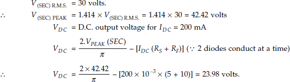
Calculation of the output ripple voltage
Ripple factor for full wave rectifier ![]()
∴ Output ripple voltage = 0.48 × VDC = 0.48 × 24.1 = 11.568 volts.
Example 4 For the reverse saturation current of I0 or IS of 5 μA; calculate the forward current IF at room temperature of 300 K, for applied voltages VF of 0.25 volts and 0.35 volts for both germanium and silicon diodes, respectively.
Solution
DATA:
Voltage equivalent of temperature VT = ![]() = 0.026 V = 26 mv η = 1 for germanium diode and η = 2 silicon diode and η = 2 silicon diode
= 0.026 V = 26 mv η = 1 for germanium diode and η = 2 silicon diode and η = 2 silicon diode
Reverse Saturation Current I0 or Is = 5 μA
Forward current IF for germanium diode
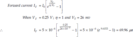
Forward current IF when VF = 0.35 Volt; η = 1 and VT = 26 mv
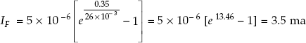
Forward current IF for silicon diode
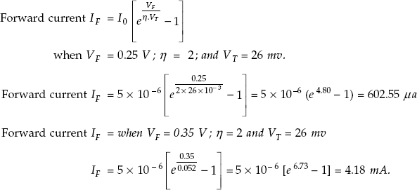
Example 5 In a P-N junction germanium diode, find the value of the voltage for which the reverse current I0 will reach 75% saturation value at the room temperature.
Solution As per the semiconductor diode current equation
For germanium diode η = 1 and VT = 26 mv
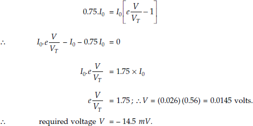
Example 6 Obtain the factor by which reverse saturation current of a germanium diode is multiplied when the operating temperature increased from 20°C to 90°C.
Solution The reverse saturation current of a diode doubles for every 10°C rise in temperature.
If I0 = I01 at T = T1
Then, at a temperature T; I0 is given by
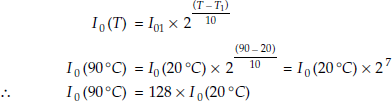
∴ The multiplication factor is 128.
Example 7 Calculate the ratio of current for forward bias voltage of 0.04 V to the current for the same magnitude of reverse bias.
Solution The ratio of current IF for forward bias V = 0.04 V to the reverse current Ir for the same magnitude of the reverse bias voltage V = 0.04.V
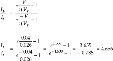
Example 8 The voltage across a silicon diode at room temperature of 300 °K is 0.7 volts when 2 mA of current flows through it. If the voltage increases to 0.75 volts, calculate the diode current when the voltage equivalent of temperature VT = 26 mv = 0.026 volts.
Solution Voltage across silicon diode; VD = 0.7 V; Current through the diode; I = 2 mA;
VT = 26 mv.
To calculate I0

Reverse saturation current calculated, I0 = 0.4 × 10⁻¹⁴
If the diode voltage increases to 0.75 volts
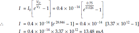
when the diode voltage has increased to 0.75 volts, current, I =13.48 mA.
Example 9 State and briefly explain the law of junction of a P-N diode.
Answer Let P represent the equilibrium concentration of holes on the P-material of P-N diode. The holes enter at the P-N junction of the diode at X = 0 into the N-region and they become the injected minority carrier hole concentration. Notionally, the concentration of holes entering the N-region at the junction at X = 0 is termed as Pn (0).
This equation is called as law of junction; at the boundary of the P-N junction formed by the P-type and N-type semiconductor materials of the P-N diode. This law indicates that injected minority carrier hole concentration Pn (0) at the P-N junction into the N-material is obtained by multiplying the equilibrium minority concentration Pn0 by ![]() . That is, the injected carrier current due to holes Pn (0) exponentially increases with respect to applied forward bias voltage V. An extention of this law leads to the derivation of the famous diode equation
. That is, the injected carrier current due to holes Pn (0) exponentially increases with respect to applied forward bias voltage V. An extention of this law leads to the derivation of the famous diode equation
Example 10 Explain the concept of cut-in voltage of P-N junction diode.
Answer Because of the contact between the two blocks of P and N materials, diffusion processes start. This is because of excess majority carriers that are holes on the P-material side, face very few holes (minority carriers) on the N-material side, resulting in a concentration gradient. This incidentally builds a charge gradient as well, as shown in the Fig. 1.
The concentration gradient among holes on either side of the junction makes the holes in the P-material move towards the N-material crossing the junction of the two materials. Similarly, the concentration gradient among electrons on either side of the junction causes the electrons in the N-material move towards the P-material crossing the junction. However, this process cannot continue forever. As the holes and electrons migrate into the other regions, the hitherto covered immobile ions on either side of the junction get uncovered. The mobile charges encountering the opposite charges may recombine leaving a no-mobile charge domain nearer the junction. This region, deplete of mobile charges is called the depletion region, transition region and space charge region.
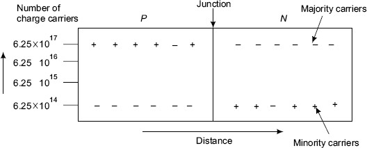
FIGURE 1 Concentration of holes and electrons in P-type and N-type materials
The uncovered immobile charges (immobile ions) develop a potential gradient with fixed negative charge on the P-side and fixed positive charge on N-side. The tendency of this charge is to oppose movement of electrons into the P-region (mobile negative electrons encountering immobile negative ions). The same thing happens to the holes trying to move into N-side. Still, the migration continues further till the immobile charges are sufficiently strong enough to prevent further progress of mobile charge movement. An equilibrium condition is established which creates a barrier for further movement of mobile charges. This barrier potential is also known as space charge potential, depletion potential, transition potential, and contact or built-in potential. This contact potential or built-in potential around the junction is of the order of 0.2 to 0.3 volts for germanium diodes and 0.5 to 0.7 volts for silicon diodes. When the diode is forward biased, the barrier potential V0 is decreased by the amount of external bias voltage and hence constitutes a continuous current called forward current If. Thus, the conduction of the device starts only when the forward bias overcomes the barrier voltage or transition potential. This potential is known as cut-in voltage and that is equal to the barrier potentials. The minimum potential before which the forward current If is negligible is termed Vγ, known as cut-in voltage, offset voltage or threshold voltage depending upon the application of the semiconductor diode. It is about 0.5 to 0.7 volts for silicon diode and 0.2 to 0.3 volts for germanium diode at 300K.

FIGURE 2 Depletion region widths in P and N type materials
Example 11 Explain the method of obtaining cut-in voltage from V-I characteristics of forward biased diode.
Answer For a P-N junction diode, the diode current  where η = 2 for silicon diode for small currents and η = 1 for large currents and for germanium diode. The factor η = 2 in the expression for silicon diode decides the rate of rise of current in the vicinity of cut-in voltage to be used as shown in Figure. 1.
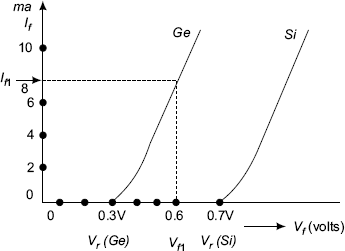
FIGURE 1 Forward characteristics for germanium and silicon diodes
The minimum potential before which the forward current If is negligible is termed Vr, known as cut-in voltage, offset voltage or threshold voltage depending upon the application of the semiconductor diode. It is about 0.5 to 0.7 volts for silicon diode and 0.2 to 0.3 volts for germanium diode at 300°K.
Example 12 Cause of surge in rectifier circuits using capacitor filter and the method of limiting the surge current.
When a sinusoidal alternating voltage with positive and negative half sinusoids is rectified the resulting output is a unidirectional voltage consisting of half sinusoids in only one direction above the time axis. It is not a desired D.C. voltage. Hence, filter circuits are used to achieve the goal of conversion of A.C. to D.C. using the combination of rectifier circuit and filter circuits. One of the basic and simple filter circuits for most of the general purposes is the simple capacitor filter and a load resistor RL across one of the rectifier circuits whether a half-wave rectifier or a full wave rectifier or a bridge rectifier depending on the demand of various features of the individual circuits.
Consider-half wave rectifier with simple capacitor filter circuit. During the interval 0 to 90° or the first half sinusoid, the filter capacitor is almost charged to the peak value of the rectified half sinusoid when the semiconductor diode is forward biased. Voltage across the capacitor VC = VP(SEC) – VD. During the interval 90° to 180° of the positive half sinusoid and during the negative half-cycle applied to the anode of the diode, the voltage across the capacitor is of such polarity that the diode is reverse biased. So, the capacitor discharges though RL till such time the diode is forward biased again. The cycles of events repeat in the operation of the filtering process to reduce the A.C. content and in turn produce D.C. voltage to the designed level.
The diode in the half-wave rectifier circuit with the shunt capacitor filter does not conduct continuously as explained above, but repeatedly allows pulses of current to recharge the capacitor each time the diode is conducting under forward biased situations at different instances of time. The current pulse is known as the repetitive surge current. The highest surge current occurs when the A.C. supply is first switched ON to the rectifier circuit. At the time of switching ON the capacitor acts as a short circuit and the surge current is at its maximum value.
So as to limit this surge current in the rectifier circuits a small value of surge current limiting resistor RS of the order of 250 ohms with high wattage power dissipation capability is connected in series path to the diode in the rectifier circuit. Value of the surge current limiting resistor RS is calculated as the ratio of the peak secondary voltage to the peak value of the expected or rated surge current from the diode specifications
Example 13 Explain Zener effect and Avalanche breakdown phenomena.
There are two types of diodes going under the name of Zener diodes
- Zener or high field diodes with narrow junctions.
- Avalanche diodes or wide junction diodes.
The reverse bias breakdown voltage of a P-N junction can be varied by suitable or necessary concentrations of doping for P-type and N-type materials. By varying the doping concentrations, diodes with specific breakdown voltages ranging from less than one volt to several hundred volts can be manufactured. If the reverse bias applied to a P-N junction is increased to a large value, the electric field intensity increases to a very high value.
It is observed that if the transition region or the depletion region width is of the order of a few μ metres; voltages in the range of fraction of a volt can create very high fields. If the doping is heavy, the depletion region width decreases further and the electric field intensity becomes higher.
For instance, if v = 0.5 volt and depletion or transition width = 0.01 micron, the field intensity is
A field of such high magnitudes can directly disrupt the covalent bonds and enhance the current to high proportions. In addition, the disrupted covalent bonds producing electron-hole pairs will allow the electron-hole pair to get accelerated by these high fields and a landslide can occur. This is called Avalanche multiplication. The line of demarcation between Zener and Avalanche breakdowns is very thin but yet a distinction can be made between the two.
The Zener effect (tunnelling phenomenon) is considered to be a narrow junction high field phenomenon similar to field emission. As a result of very high field intensities of the order of 107 volts/m some electrons are pulled across the forbidden band gap from valance band energy levels to conduction band in diodes having narrow depletion region widths. The electron tunnels through the barrier as a wave instead of acquiring the sufficient band gap energy to cross the barrier as a particle. This phenomenon is known as the Zener effect.
Avalanche breakdown On the other hand, in a wider junction due to larger mean free paths the charge carriers acquire kinetic energy, sufficient enough to disrupt the covalent bonds and start a cumulative process. This process of charge carrier multiplication is similar to secondary electron emission as in X-ray production. This is Avalanche effect (impact ionisation). Paradoxically, the Zener breakdown occurs at lower voltages and the avalanche breakdown occurs at higher voltages.
When a diode is designed for a required and specific breakdown voltage, the device is called as breakdown diode. If the P-N junction of a breakdown diode for a specified breakdown voltage is well designed, the breakdown will be sharp and the current after breakdown will essentially be independent of the voltage (rated breakdown voltage).
Example 14 Define and explain diffusion current and drift currents.
Diffusion
The Fig. 1 shows a material in which the concentration is non-uniform and decreases with distance. This change in concentration with distance is named concentration gradient and allows charge movement because of concentration variation. This process of movement of charges from regions of greater concentration to regions of smaller concentration is called diffusion. Due to this charge movement, a current density Jp is proportional to the concentration gradient ![]() appears and it is expressed as a relation.
appears and it is expressed as a relation.
where DP is the diffusion constant for holes, measured as m2/sec.
The negative sign in the equation (1) appears because of the fact that with distance x, the concentration is decreasing. Since electrons can be considered as duals of holes, current density for electrons due to concentration gradient ![]() ;
;
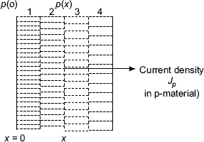
FIGURE 1 Diffusion
Einstein relation
The mobility µ and diffusion D are both statistical phenomena and a correlation should exist between them. Einstein has expressed this in the following manner. This goes under the name Einstein relationship.
Einstein relationship expresses the relationship between diffusion constant DP and mobility µ in the following manner:
VT is called voltage equivalent of temperature. The significance of VT can be explained as follows.
Since, temperature causes thermal agitation resulting in movement of charges; VT can be expressed as a voltage, which also causes movement equivalent to that produced by temperature and thus it is called as volt equivalent of temperature.
Net current
In the semiconductors drift current exists due to potential gradient and diffusion current due to concentration gradient. So, the total current should be the algebraic sum of both these currents as expressed below:
and,
Example 15 Draw the energy band diagrams for a P-N diode
The energy band diagram for a P-N junction appears as follows:
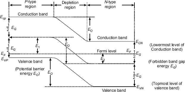
FIGURE 1 Energy band diagram of a P-N junction.
Explanation
When P and N materials are brought into contact, the diffusion and drift processes start and equilibrium is reached till the Fermi levels on both sides are aligned. This pushes down both the conduction and valence band energy levels producing a difference in energy levels equal to Eo. This causes a potential difference Vo to be developed across the space charge region and is called the contact difference of potential or built in potential. The quantitative relation can be obtained in terms of energy level as follows. According to the diagram, the shift in energy levels
E0 = Ec.p – Ec.n = Ev.p – Ev.n = E1 + E2. This E0 represents the potential energy associated with the electrons at the junction.
Example 16 Draw the sketches of charge density, electric field intensity and potential energy barrier of a P-N diode.
Open Circuited Junction of P–N Diode
When an intrinsic semiconductor wafer (like silicon or germanium) is doped by acceptor (P) and donor (N) impurities from either side a P-N junction is formed. The Fig. 1 shows the formation of the materials. On the P-material side immobile negative charges and mobile positive charges (holes) appear. Similarly, on the N-material side immobile positive charges and mobile negative charges (electrons) appear. These mobile charges (majority carriers) cross the junction due to concentration gradient. This movement causes exposure of immobile charges, or ions on either side of the junction. On the P-material side, negative charges, which were neutralised by the mobile holes due to the migration of mobile holes get uncovered. The same thing happens with the immobile positive charges and the mobile electrons on the N-material side. This leads to the formation of a potential gradient. This is called as the contact, diffusion, barrier, depletion or space charge potential designated as V0.
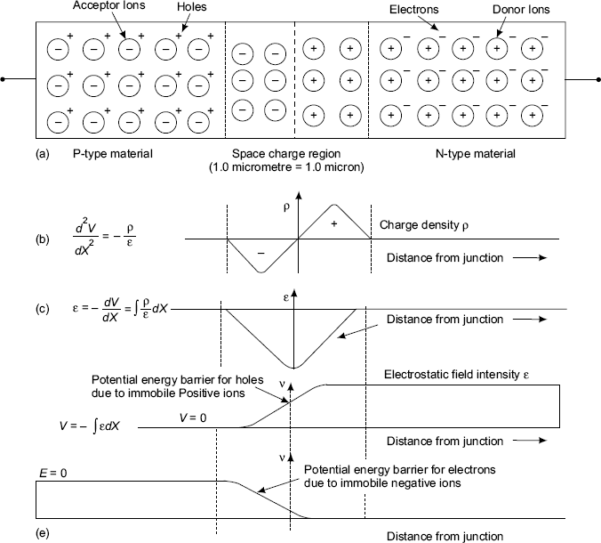
FIGURE 1 Sketches of charge density (ρ), electric field intensity (ε) and potiential energy barriers (v) for electrons and in a P-N diode
In the absence of any excitation as explained earlier the contact potential V0 is developed at the junction of the P-N diode. In the profiles the various involved quantities, charge density, electrostatic field intensity and potential energy barriers for electrons and holes at the junction contributing to the contact potential V0 are as shown in the Fig. 2.
Example 17 Explain the reasons for the variation of the reverse saturation current I0 or IS of a semiconductor diode with temperature.
Explanation for the variation of reverse saturation current of a diode with temperature T:
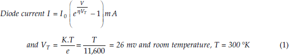
Since I0 as well as V T are temperature dependent as can be seen by above equation (1), both are taken into consideration for arriving at variation of I0 with temperature. It is also known that the intrinsic concentration ni2 is temperature dependent and it is expressed as,
where, VG 0 is voltage numerically equivalent to band gap energy and VT is the electronvolt equivalent of temperature. It is of the order of 26 mv at room temperature.
In the expression for I0; the diffusion constants are involved and varying inversely with temperature. The temperature dependence of I0 can be expressed as ![]()
In the discussion up to now, the generation and recombination of electron-hole pairs in the space charge region is neglected and is true for germanium but not for silicon.
So, the expression for the current I has to be modified as
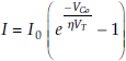 ; where η = 1 for large currents and η = 2 for small currents.
Also, it is practically found that I0 is directly proportional to ni but not ni2.
All these conditions can be expressed to get ![]()
Generally, this relation can be expressed as
For germanium device η = 1; m = 2 ; VG0 = 0.785 V.
And, for silicon device η = 2; m = 1.5 VG0 = 1.21 V;
Taking logarithms on both sides for the following equation.
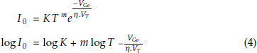
We know that
Using the value of VT from equation (5) in the equation (4)
Differentiating the equation (6) with respect to temperature T
Again, using the value of VT from equation (5) in (7)
The reverse saturation current doubles for every 10°C raise in temperature both for germanium and silicon devices approximately.
Using the equations (3) and (7) it can be derived that V also is dependent on temperature and approximately varies as shown in the following expressions:
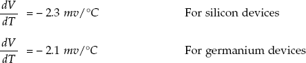
For practical design considerations it is assumed as
The equation (9) suggests that
![]() decreases with increasing temperatures for the semiconductor diodes.
decreases with increasing temperatures for the semiconductor diodes.
Example 18 Draw the energy band diagrams for P-N diode without any bias, with forward bias Vf and reverse bias conditions and explain the effects of biasing conditions on the variations in barrier potential and depletion region widths.
Solution Energy band diagram of semiconductor diode for no bias situation.
When P and N materials are brought into contact, the diffusion and drift processes start and equilibrium is reached till the Fermi levels on both sides are aligned. This pushes down both the conduction and valence band energy levels producing a difference in energy levels equal to Eo. This causes a potential difference Vo to be developed across the space charge region and is called the contact difference of potential or built in potential. The quantitative relation can be obtained in terms of energy level as follows. According to the diagram, the shift in energy levels
The valence band energy level EVN and conduction band energy level ECN in N-type semiconductor material are at slightly lower energy levels than the valence band energy level EVP and the conduction band energy level EVP in a P-type material as shown in the energy band diagrams of P-N junctions. This difference in energy levels is due to the differences in the energy levels of the dopant atoms used to form the P-type and N-type extrinsic semiconductors.
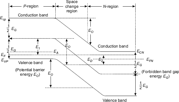
FIGURE 1 Energy band diagram of a P-N junction with no bias
In Fig. 2 showing the energy band diagram for a P-N diode with forward bias Vf, it can be seen that there is a reduction in the contact or barrier potential and also the depletion region width of the forward biased diode is reduced corresponding to the magnitude of the applied bias.
In Fig. 3 showing the energy band diagram for a P-N diode with reverse bias Vr, it can be seen that there is an increase in the contact or barrier potential and also the depletion region width of the reverse biased diode increases corresponding to the magnitude of the applied bias.
Energy band diagram of a P-N junction diode with forward bias Vf is shown in Fig. 2 with reduced potential barrier and depletion region widths.
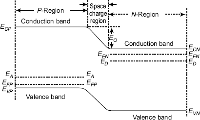
FIGURE 2 Energy band diagram of a P-N junction with forward bias Vf
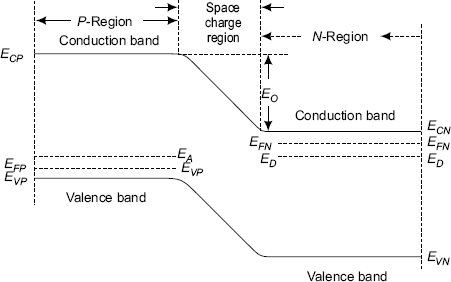
FIGURE 3 Energy band diagram of a P-N junction with reverse bias Vr
Energy band diagram of a P-N diode of a reverse biased P-N junction is shown in the Fig. 3 with increased potential barrier and depletion region widths.
Example 19 Discuss the necessity of the use of filter circuits with rectifier circuits.
Necessity of filter circuits with rectifier circuits
It is observed that the output of a rectifier is a pulsating D.C. consisting of a D.C. component and superimposed ripple (A.C. content). In most cases a pure D.C. or a D.C. with tolerable ripple is needed. A way to eliminate or reduce the ripple to the required level is to use a filter.
Since the reactive elements, inductors and capacitors respond to D.C. and A.C. differently these can be used to reduce A.C. content relative to D.C. in the rectified output voltage. Filtering process is done using low pass filters which are suitably connected capacitors, inductors and a combination of them such as shunt capacitor filter, choke input filter, L-Section filter and π-section filters depending on the purity of D.C. required or the level of ripple content that can be of no problem in a particular application. Thus, a power supply filter reduces the magnitudes of all the alternating components or the ripple content in the rectified output wave forms and passes the D.C. content. Ripple factor is used as a measure of effective functioning of a filter circuit. Ultimately, for good filter circuits ripple factor should be as small as possible indicating the reduction of A.C. component in the filtering process.
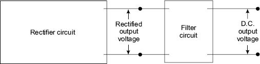
FIGURE 1 Combination of rectifier and filter circuits for D.C. sources
Example 20 Compare the performance of various types of filter circuits. List out the different types of filter circuits and merits and demerits of various filter circuits.
Inductor filter
An inductor opposes changes in current and thus the pulsations keeping a series inductance in the filter circuit can smoothen out, for example, the ripple content in the rectified output voltage fed to the filter circuit
Ripple factor ![]() ∴ Ripple factor will be small for low values of load or for large values of load currents and high values of inductances (L).
∴ Ripple factor will be small for low values of load or for large values of load currents and high values of inductances (L).
Shunt capacitor filter circuits
This simple and usual filter circuit uses a capacitor connected in parallel with the load resistance RL. A capacitor connected in shunt across the load resistance provides a bypass path for A.C. component or ripple content present in the output voltage of the rectifier circuit and the ripple gets reduced
![]()
Ripple factor

From this expression for the ripple factor, it can be inferred that with increasing values of the capacitance C and RL, the ripple gets reduced. That is, for smaller values of IDC and large values of capacitance, ripple content will be less and smoother will be the output wave form.
L-section filter circuit
Here, the ripple factor is independent of the load currents. Hence, L-section filter is used in applications having wide variations of load currents
π-Section Filter Circuit
The ripple is very much reduced by the double filtering action.
As the current increases for an L-section filter the voltage quickly drops and then changes more smoothly, since the inductance L smoothens the varying current. Also, the ripple is less dependent of load current. This L-section filter circuit is useful for large fluctuating loads. On the other hand, a π-section filter has always a relatively high D.C. voltage up to IL0; the optimal load current. Thus, π-section filter circuit is preferable for light (small) fixed load currents, since it provides high D.C. relatively.
Example 21 Discuss the general specifications of P-N junction diodes.
Answer Depending upon the application of the diode in the practical circuits, the required maximum voltage, current, power, peak inverse voltage, surge currents and temperature withstanding capability are identified. Once the temperature range of the device working environment is decided, the selection and the usage of silicon diode or germanium diode is decided based on the cost of the practical application also in mind.
Then, for the selection of the diode with the desired operating characteristic features in the application, the device manuals with the specifications are consulted for safe working of the device, so that the selected device has maximum ratings well above the desired quantities. Further, the ratings of the devices are also function of the usage of the device, whether used as rectifier diode, switching diode or in power handling circuits. The general specifications are as following:
- Operating temperature range Tj or TA.
- Maximum forward current rating of the device I0 or IF.(AV) the device can withstand.
- During the reverse bias operation, the required operating reverse bias should be well below the breakdown voltage rating of the selected diode so that the device operation is in safe limits. VBR.M rating for the device is to be considered or rms reverse voltage VR.
- During reverse bias across the diodes used in rectifier circuits, the peak inverse voltage rating varies based on the type of the rectifier circuits. Once the required PIV is known, the selected diode PIV rating should be much above this.
- Similarly, peak surge current rating IF.M.
- Maximum forward voltages drop VF for mentioned forward current and device temperature.
- Power dissipation P the maximum power the device can safely dissipate without heat sinks.
- Maximum reverse current Ir.
- Non-repetitive peak surge current IFS.M that occurs during initial charging of the capacitors for a brief time in rectifier with capacitor filter circuits that is greater than the maximum forward current rating of the device.
Example 22 Draw the circuit of a full wave bridge rectifier circuit. Explain the principle of working of a bridge rectifier circuit.
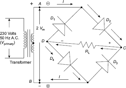
FIGURE 1 Bridge rectifier circuit
Full wave bridge rectifier circuit using four diodes and a transformer without the necessity of centre tapped secondary winding.
When the upper terminal A of the transformer secondary is positive during the half-cycle 0 to π of the secondary voltage, diodes D2 and D4 conduct (diodes D3 and D1 are reverse biased) in series developing a D.C. voltage across the load RL with terminal C positive.
On the other hand, during π to 2π interval of the transformer secondary voltage, when the terminal B is positive diodes D3 and D1 conduct in series (diodes D4 and D2 are reverse biased) and the current flowing through RL in the same direction making the terminal C of the load positive again. Thus, the two currents flow through the load resistance in the same direction to increase the output D.C. voltage. The secondary current is present during both halves of the secondary voltage, thus the transformer is fully utilised.
The advantage of this configuration is that it gives twice as much D.C. as compared to full wave rectifier circuit for the same secondary of the transformer. Further, with reduced size of the semiconductor diodes, the use of four diodes in the bridge rectifier circuit has become popular as a package. The ripple factor and regulation are same as that of full wave rectifier.
The peak inverse voltage PIV is the same as the half-wave rectifier, that is, Vm across each diode. Disadvantages are 1) Since the two diodes are in series during conduction, twice the voltage drop reduces the output voltage. 2) It needs four diodes.
The signal wave forms across the load resistance RL for the applied input signal voltage and for different situations of conducting diodes in the bridge rectifier circuits are shown in the following page.
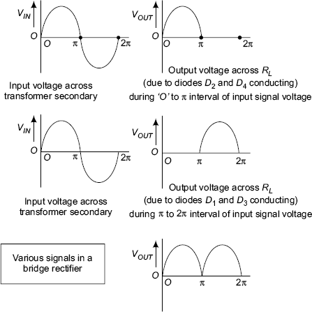
FIGURE 1 Output voltage across RL for bridge rectifier acting as an F.W. rectifier
Example 23 Define the concept of regulation in rectifier circuits and also define percentage regulation. Verify with necessary equations that the regulation of full wave and half-wave rectifier circuits depends on the ratio of forward resistance Rf to the load resistance RL.
Solution The variation of D.C. output voltage of a rectifier circuit from no load output voltage VDC.(noload) to the output voltage with variations in the D.C. load current expressed with reference to full load D.C. output voltage is known as regulation.
For Half wave rectifier % Regulation is a function of the ratio of Rf to RL as shown

For half-wave rectifier % regulation is a function of the ratio of Rf to RL as shown
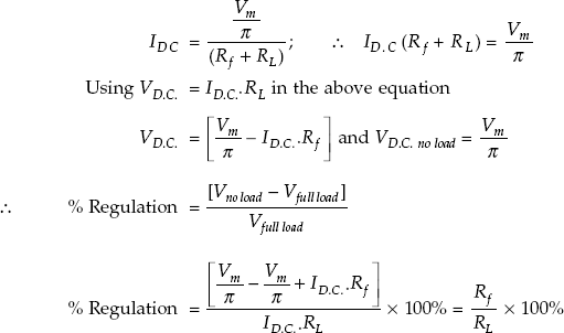
The above derivation is also true for full wave rectifier circuit.
Example 24 Discuss the applications of Hall effect.
Answer
- To determine type of semiconductor.
- To measure the mobility of charge carriers.
- To measure carrier concentrations in semiconductor materials.
- To measure strength of magnetic flux density B.
- Hall effect sensors can be used as proximity probes in instrumentation applications.
- For measurement of speed of a turbogenerator in power plants.
- Computer key board switch (Hall effect switch gives an output if a magnet is brought near a special type conductor) for locking and unlocking the keyboard operations.