Chapter 4
Amplifiers Using Bipolar Junction Transistors or FET
The most important application of a BJT (bipolar junction transistor), or a FET (field effect transistor) is to act as an amplifier. Each amplifier stage consists of an active device a BJT or a FET, D.C. source, A.C. source and associated circuit components. To understand certain basic amplifier features such as amplification of signals, input and output impedances, frequency response of amplifiers, and so on. Block Box model of an amplifier is discussed initially.
An amplifier can be treated as a two-port network with two terminal pairs; one pair of input terminals and one pair of output terminals. In most of the cases, there is a common terminal between the input and the output ports called the ground node (ground terminal) G as shown in the Fig. 4.1.
As shown in the Fig. 4.1, between 1 and 2 input pair of terminals, a voltage or current source can be connected and the input quantity can be Vin or Iin. Similarly, at the output pair of terminals, an output voltage Vout (output voltage) or output current Iout is developed irrespective of the nature of the source; there will be both Vin and Iin and these are interrelated by Thevenin’s and Norton’s theorems. If the output quantity is more than the input quantity, the two-port network is said to function as an amplifier.
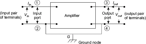
FIGURE 4.1 Amplifier as two-port or four terminal network
AV and AI are both dimensionless quantities.
In addition to AV and AI; two more quantities known as output impedance Zout and input impedance Zin are also defined.
The reciprocals of Zin and Zout also will be useful in active network analysis.
If, Vout < Vin or Iout < Iin the two-port network is known as an attenuator.
4.1 BJT and FET More Often used in Amplifiers
For instance, the public address system is used to make the sound from an individual, audible to a large gathering by first converting the sound energy into electrical signal voltage of the order of a few hundred to a few thousands of microvolts by a microphone. This electrical signal is given as an input to a two-port network acting as an amplifier with gain AV.
This two-port network will have an active device such as a bipolar junction transistor or a field effect transistor and an associated circuit. The output signal Vout from the amplifier is an enhanced version of the input signal, say, an electrical signal output from a microphone and is used to drive a loudspeaker system. The loudspeaker system converts the amplified electrical signal (Vout = AV Vin) back into amplified sound.
This public address system can be represented as shown in Fig. 4.2.
VMike = Voltage from the microphone (transducer) called the source voltage.
ZMike = Self-impedance of the microphone.
ZSpeaker = Self-impedance of the speaker (transducer) which acts as a load ZL to the amplifier.
For instance,
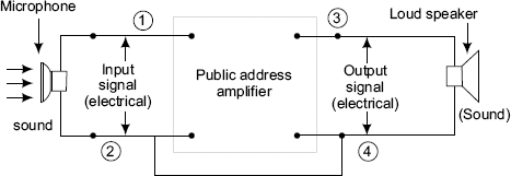
FIGURE 4.2 Example of public address amplifier

FIGURE 4.3 Amplifier and the transducers
This expression in the equation (4.5) shows that unless ZMike is negligible compared to Zin; Vin will be lower than VMike.
When a FET is used as an amplifying device, since its input impedance Zin is theoretically infinite (Zin is of the order of hundreds of megaohm) Vin = VMike. This discussion suggests that the input impedance of an amplifier should be infinite or very large compared to the source impedance Zs; (Z Mike in this specific application) when excited by a voltage source. On the other hand, if the exciting source is a current source,
where IS is the magnitude of the current of the current source.
It can be inferred from the above expression that to maximize Iin; either Zin should be zero or Zs should be theoretically infinite or very large compared to Zin.
Similarly, to get a maximum voltage at the loud speaker or at ZL; Zout > zero (Zout should tend to zero). The significance of Zout and Zin for two-port network acting as an interface is well established. One more important point is that if two-port network acts as a controlled current source, its self-impedance should tend to infinity or the load impedance ZL should tend to zero. (To get maximum current for a load from a current source, the load impedance should tend to zero. This finds use in the future analysis in maximising the current gain from an amplifier. Similarly, when an amplifier is designed to get maximum voltage output, the load impedance should tend to infinity or several orders high compared to Zout of the amplifier).
A brief description of the components of a basic amplifier with an active device It was seen in the characteristics of the BJT and FET devices that (for an active device together with circuit components to act as an amplifier) for an amplifier, it should operate in the active region of the output characteristics. For BJT, this requires that the input junction is forward biased and the output junction is to be reverse biased. (An acronym can make the remembrance easy by saying IFOR active; this can be interpreted as I for input junction, F for forward bias; O for output junction and R for reverse bias. This means that to maintain a transistor in the active region of the output characteristics, the input junction is to be forward biased and the output junction is to be reverse biased immaterial of whether it is N-P-N or P-N-P transistor). Fig. 4.4
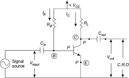
FIGURE 4.4 Basic common emitter transistor amplifier circuit
A transistor amplifier will have two types of operating conditions, with the D.C. and the A.C. voltages. And so, it has a D.C. equivalent circuit and an A.C. equivalent circuit.
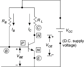
FIGURE 4.5 D.C. equivalent circuit for CE transistor amplifier
RL (load resistor) and RB (base resistor) are so chosen to maintain the transistor in the active region at a convenient base current and collector current as required for the specific class of operation of the amplifier based on the application of the amplifier circuit.
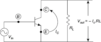
FIGURE 4.6 A.C. equivalent circuit for common emitter (CE) transistor amplifier
Generally, amplifiers get alternating signals for input signals Vin. The amplifiers are expected to develop proportionate and increased output A.C. signals Vout at the output port of the amplifier.
So, A.C. and D.C. versions of the equivalent circuits differ in that capacitors are used to separate A.C. and D.C. components. In D.C. circuits they are considered as open circuits (Xcin or Xcout = ![]() = ∞ for). In this context of blocking D.C. voltages, they are called as blocking capacitors CB.
= ∞ for). In this context of blocking D.C. voltages, they are called as blocking capacitors CB.
In A.C. signal operations the capacitors are expected to function as short circuits and couple the A.C. signals from the signal source to the input port and output port of one stage to the input port of other stage. They are called coupling capacitors CC in this context. The capacitor that connects the A.C. input signal at the input port of the first stage of amplifiers is known as Cin. The capacitor that connects the A.C. signal from the output port of an amplifier to the load is known as output coupling capacitor Cout.
4.2 Transistor Biasing Methods
The simplest method to maintain a bipolar junction transistor (BJT) in the active region is to use two separate D.C. sources as shown in the Fig. 4.7. One D.C. supply VBB between the base and emitter with a series resistance RB is used to maintain the required base current (forward bias VBE to forward bias the input junction, the emitter junction of the transistor). A second D.C. supply VCC between collector and the emitter is used to maintain reverse bias to output junction that is the collector junction of the transistor. This method of biasing makes the transistor to behave as an amplifying device.

FIGURE 4.7 Two separate D.C. sources for biasing the N-P-N transistor
Instead of using two separate D.C. supplies, one D.C. supply VCC in combination with a few resistors, three types of biasing circuits were developed, (1) fixed biasing circuit, (2) collector to base biasing circuit, and (3) potential divider biasing or self-biasing circuit.
The type of biasing circuit in use depends upon the class of operation of the amplifier and bias stability requirements of the circuit which are discussed one by one in a logical sequence.
Fixed Bias Circuit
Using a single D.C. source VCC with a reorientation of RB of the circuit in the Fig. 4.7 will be sufficient for properly biasing the transistor that is to provide forward bias VBE to input junction, the emitter junction of the transistor and the reverse bias to the output junction, the collector junction of the transistor (the type of biasing voltages also depends on whether it is an N-P-N or P-N-P transistor and the type of connection of the transistor CE, CB or CC configuration of operation of the transistor). This arrangement is called the fixed bias circuit, or fixed current bias circuit as shown in the Fig. 4.8.

FIGURE 4.8 Fixed bias circuit for common emitter transistor
The fixed bias or base bias circuit uses only a single D.C. source or supply voltage VCC (for example, from a transistor power supply) and two resistors RL (or RC) and RB so as to provide the required magnitudes of forward bias (FB) to the input junction (emitter junction between the base and the emitter areas) of the transistor. Simultaneously, reverse bias (RB) is available to the output junction (collector junction between the base and the collector areas) of the common emitter connected transistor.
Fixed Bias or Base Bias Circuit for Common Emitter (N-P-N) Transistor
The choice of RL and RB is not entirely arbitrary, but it is subjected to some design constraints. For instance, VCC should always be less than VCE max, as prescribed by the specifications given by the manufacturer of the active devices.
In addition to this, the second point to be considered is that the power dissipation VCE.IC at the collector junction of the transistor should always be less than the allowed maximum power dissipation specified by the manufacturer. This design constraint is represented by a curve drawn on the output characteristics called as the power dissipation curve. This requires that the D.C. load line XY should always be below the power dissipation curve. These details are shown in the Fig. 4.9. This is assured if VCEQ1 is less than or equal to ![]() for small signal operation of the amplifier.
for small signal operation of the amplifier.
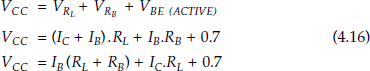
Under these circumstances, the following KVL equations can be written. At the output circuit loop ACEA
VCC = VRL + VCE
VCC = ICRL + VCE
VCC − VCE = ICRL ---- D.C. load line equation. (4.7)
This equation (4.7) represents the equation of a straight line known as D.C. load line equation. This has a negative slope of ![]() as shown in Fig. 4.9
as shown in Fig. 4.9

FIGURE 4.9 D.C. load line and quiescent operating point on transistor output characteristics
In equation (4.7); if IC = 0 mA, then VCE = VCC, and this represents one point, say, Y with the coordinates (VCE = VCC; and IC = 0).
At point X; VCE = 0 volts then ![]() So, the coordinates of X are
So, the coordinates of X are ![]() . Joining the two points X and Y; the D.C. load line is drawn on the transistor output characteristics as shown in the Fig. 4.9.
. Joining the two points X and Y; the D.C. load line is drawn on the transistor output characteristics as shown in the Fig. 4.9.
From Fig. 4.8 using KVL equations for the input side loop ABEA
VBE active = 0.3 volts for germanium transistor
VBE active = 0.7 volts for silicon transistor
when VBE active << VCC as is the case in most applications.
The current IB is constant and so this type of biasing network is called as fixed bias circuit.
Under no signal conditions, the D.C. operating point will be the point of intersection of the VCE versus IC characteristic for ![]() and the D.C. load line. This load line is to be located below the power dissipation characteristic (power dissipation curve can be drawn from the maximum power dissipation rating of the selected transistor) for safe operation. The quiescent operating point Q (bias point) is determined graphically, knowing the class of operation of the amplifier in which the transistor amplifier circuit is to be used. The quiescent or D.C. operating point Q1 is fixed at the middle of D.C. load line for class A operation of amplifier.
and the D.C. load line. This load line is to be located below the power dissipation characteristic (power dissipation curve can be drawn from the maximum power dissipation rating of the selected transistor) for safe operation. The quiescent operating point Q (bias point) is determined graphically, knowing the class of operation of the amplifier in which the transistor amplifier circuit is to be used. The quiescent or D.C. operating point Q1 is fixed at the middle of D.C. load line for class A operation of amplifier.
Shift in DC Operating Points Q1 The D.C. operating point shifts due to temperature variations as well as variations due to device parameters in case of replacement of the active device.
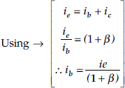
Since IC = − αIE + ICO and IC = βIB + (β + 1) ICO
Even if, IB is constant, IC can change due to changes in β or ICO. In a circuit, if a transistor fails and is replaced by a new transistor, for the same IB; IC is now β2IB and may be more or less than the previous value if β2 is the β of the new transistor. Similarly, if the collector current IC, is IC for temperature T1, and if the temperature rises to T2; IC will be now IC2 such that IC2 ≠ IC.
Even then the operating point Q1 shifts as shown in Fig. 4.10.
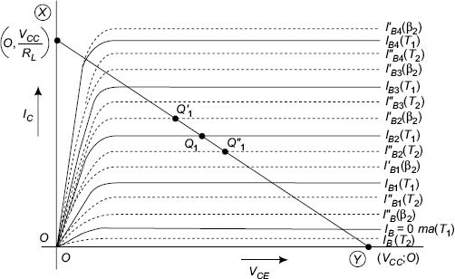
FIGURE 4.10 Demonstration of shift of operating point with changes in ‘β’ and temperature ‘T’
Let Q1 be the operating point at a particular temperature T1 and β = β1. If temperature falls to T2; Q1 is pushed down to Q″. On the other hand, if β increases to β2 due to replacement of the transistor, Q1 is pulled up to Q′. In the former case with Q″ for the same input signal drive; a portion of the output signal may be cut-off and the signal swing is reduced. If Q1 is pulled up to Q′, VCEQ shifts left and the signal swing is restricted due to the transistor entering into the saturation region.
So, to guard against these variations and making the operations stable, following techniques can be adopted. Before analysing the circuits, the stability of operating point Q is defined and criteria for stability are arrived at.
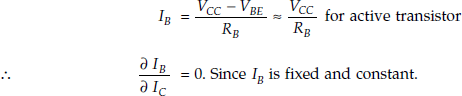
Let stability factor S be defined as
Differentiating this equation with respect to IC

Now, the stability factor

In the fixed bias circuit IB and IC are independent and the stability factor becomes (β + 1). If, IB and IC are independent; ![]() . Substituting this in the equation 4.12 for stability factor S,
. Substituting this in the equation 4.12 for stability factor S,

![]() can be justified as follows:
can be justified as follows:
For a fixed bias circuit shown in Fig. 4.8
Collector to Base Bias Circuit
In this circuit of Fig. 4.11, resistor RB is now connected between collector and base. It can be seen that stability of the quiescent operating point Q is improved as can be observed by reduction in the value of stability factor S.
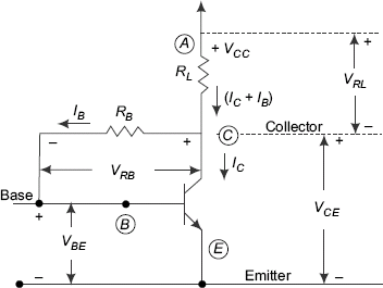
FIGURE 4.11 Collector to base bias circuit for N-P-N common emitter (CE) transistor
For the collector to base bias circuit in Fig. 4.11 (loop A-C-B-E-A)
Differentiating the above equation with respect to IC
i.e.
Substituting – ![]() for
for ![]() into the equation (4.15) we obtain the following expression for stability factor S.
into the equation (4.15) we obtain the following expression for stability factor S.
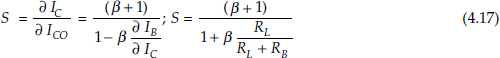
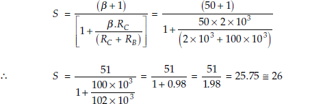
Hence, this value of stability factor S is much smaller than (β + 1), which is derived previously for the fixed bias circuit. So, there is an improvement in stability of operation with collector to base bias circuit
If RB << RL; (RL + RB) ≈ RL
![]()
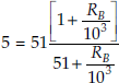
Thus if this condition is satisfied, then there is a large improvement in stability. But this becomes a practical impossibility, since IB becomes excessive when RB is very small and the device may saturate. Actually in all practical circuits RB will be a few orders greater than RL. Assuming that RB = 15 RL and substituting in the equation (4.17) for S
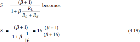
If β = 50; the equation (4.19) becomes ![]()
In this collector to base bias circuit, an additional disadvantage is that there is an unavoidable negative feedback from output port to the input port through RB; resulting in gain reduction. Also, both the output and input impedances get reduced due to this feed back through RB. This circuit has become obsolete.
Potential Divider Bias or Self-Bias Circuit
In the potential divider bias circuit of Fig. 4.12, VCC in association with R1 and R2 provide the bias and RE provides bias stability as is explained.
Thevenin’s equivalent circuit for analysis is given in the Fig. 4.13
Applying Thevinin theorem in the circuit of Fig. 4.12
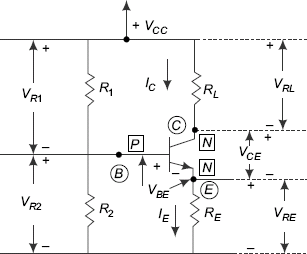
FIGURE 4.12 (Self-bias circuit) Potential divider bias circuit

FIGURE 4.13 Thevinin’s equivalent circuit suitable for analysis
(i.e. potential division of VCC between R1 and R2 i.e. open circuit voltage)
To get the equivalent Thevinin resistance RTh; short circuit the voltage source VCC. Then, the circuit is as shown in the Fig. 4.15.
RTh then is the parallel combination of R1 and R2
In the loop BDGEB,
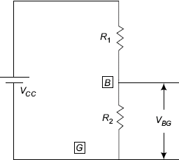
FIGURE 4.14 Thevinin equivalent circuit at input port of the transistor to find open circuit voltage VBC

FIGURE 4.15 Thevinin equivalent circuit at input port of the transistor to find RTh
Differentiating above equation with respect to IC,
Substituting this in the equation for stability S

Rearranging the terms in the above equation (4.22), ![]()
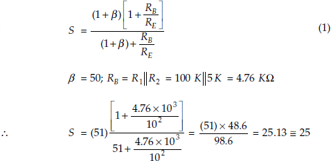
Stability factor S can be rewritten as

So, the inference is that S varies between 1 for small values of RB /RE and (1 + β) if RB /RE is very large.
It is not practically possible to make RB /RE small, since decrease in RE reduces input impedance, thus affecting the performance of the amplifier. By choosing suitable values for RB and RE, transistor-biasing circuits can be designed for desired values of stability factor S.
Generally, lower values of S are obtained with potential divider bias circuit. This circuit has more stable Q (self-correction of bias through RE in the circuit) and so this circuit is more popular than the other biasing circuits.
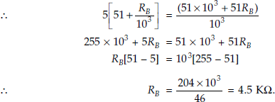
For instance, if S is to be of a prescribed value say 5 for β = 50 and RE = 1 KΩ.
By substituting these values in the above expression for S, the value of RB = 4.5 KΩ, as shown below.
 Cross multiplication results in the following expression
When this type of biasing circuit is used in a common emitter (CE) transistor amplifier circuit, a capacitor CE is connected in parallel to RE, so that A.C. signal has a bypass path through CE (XCE = 0.1 RE) at the lowest frequency of the signal to be amplified and used value for CE > 10 μf) so as to avoid reduction of effective A.C. input signal at the input port because of feedback of A.C. signal through RE if CE is not used
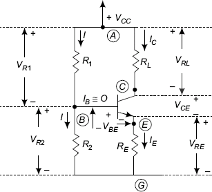
FIGURE 4.16 Analysis and design of self-bias circuit or potential divider bias circuit
Considering loop ABGA (through VCC)
Neglecting current IB through base in comparison to current I through R1 and R2.
An equivalent circuit with a Thevenin’s equivalent voltage generator VTh or VBB together with ![]() between base and ground is drawn in the following Fig. 4.17.
between base and ground is drawn in the following Fig. 4.17.
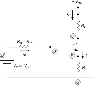
FIGURE 4.17 Analysis of self-bias circuit
From loop ABGA of the circuit of Fig. 4.14
or,
and,
Above value for R2 in the equation (4.25) is obtained from the following steps,
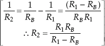
Thus, knowing RE and S, the value of RB can be calculated using the equation 4.23 and then using the equations 4.24 and 4.25, the values of R1 and R2 can be calculated.
By selecting Vcc from transistor ratings, RL and quiescent or D.C. operating point; RE can be calculated considering the loop ACEGA
Neglecting IB in comparison with IC, since hFE (D.C. Beta) is large; IE ≅ IC
Then, VCC = IC (RL + RE) + VCE
VCC − VCE = IC (RL + RE) (4.26)
This equation is known as D.C. load line equation for voltage divider bias circuit or self-bias circuit. So, the coordinates of the point X on the D.C. load line are VCE = 0 volts and ![]() the coordinates of the point Y are VCE = VCC and IC = 0 mA. This D.C. load line equation superimposed on the output characteristics of the CE transistor specify the required D.C. operating conditions corresponding to the quiescent operating point Q for the required class of operation of the amplifier circuit that are discussed in the discussion of amplifier circuit operation.
the coordinates of the point Y are VCE = VCC and IC = 0 mA. This D.C. load line equation superimposed on the output characteristics of the CE transistor specify the required D.C. operating conditions corresponding to the quiescent operating point Q for the required class of operation of the amplifier circuit that are discussed in the discussion of amplifier circuit operation.
4.3 Various Bias Compensation Circuits and their Working
For a transistor to operate as an amplifying device emitter junction is forward biased and the collector junction is reverse biased by one of the three biasing methods using a single D.C. source and a few resistors. But only the potential divider biasing circuit or self-bias circuit provides stable quiescent or D.C. operating point Q for better response of electronic circuits. But there is a loss of gain or amplification due to negative feedback through the resistor RE in the process of stabilisation of the D.C. operating conditions of the amplifier circuit.
In certain applications, this loss of gain may be put to considerable disadvantage in the operation of the circuit. One of the simplest methods of design of electronic circuits is to counteract the effect of changes in VBE (may be due to temperature variations or replacement of the active device with another value of cut-in voltage) is to make the emitter voltage VE very much greater than the required magnitude of the forward bias to the emitter junction. But, some compensation methods or techniques are used to improve the stability of quiescent operating point Q and thus resulting in extremely stable operating point meaning stable D.C. biasing voltages to the emitter and collector junctions of the transistor.
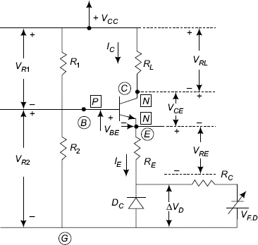
FIGURE 4.17A (Self bias circuit) Potential divider bias circuit
A compensating semiconductor diode DC applied with forward bias VF.D is included in the emitter path of the transistor biasing circuit shown in the Fig. 4.17A. The diode to be used for compensation of VBE should be of the same semiconductor material as the transistor so that the voltage–temperature coefficient is same. When VBE changes by ∆VBE with changes in temperature, the voltage across the diode DC changes by ∆VD since ∆VD = ∆VBE the corresponding changes cancel each other and compensation for changes in temperature takes place.
Diode Compensation for Variations in IC0 In case of germanium transistors, changes in reverse saturation current IC0 with changes in temperature cause a corresponding significant changes in the collector current IC that cause instability of biasing voltages of the transistor decided by the quiescent operating point. This instability is reduced by introducing a germanium diode between the base and the emitter path (the germanium diode is reverse biased by the voltage VBE of the transistor) for nullifying the increases in the reverse saturation currents with temperature changes as shown in Fig. 4.17B.

FIGURE 4.17B Fixed bias circuit for common emitter transistor with a germanium diode for compensation of IC0 for a germanium transistor
Assume the current through the reverse biased diode as IRD
Then the base current IB = (I – IRD)
Using this expression for IB in the equation for collector current IC
The reverse saturation current IRD of the compensating diode nullify the variations in IC0 of the transistor maintaining constant collector current IC and provide stable operation of the device.
4.4 Thermistor Compensation
Circuit in the Fig. 4.17C shows one method of transistor parameter variation compensation using temperature sensitive resistive elements such as thermistors rather than diodes. The resistance of thermistor devices changes with temperature. They use ceramic like semiconductors with high thermal coefficients of resistance having high sensitivity to temperature variations. Thermistor has a negative temperature coefficient; where the resistance RT of the device decreases exponentially with increase in temperature. Thermistor is connected in the CE potential divider bias circuit between positive VCC and the emitter point of the transistor.

FIGURE 4.17C (Self bias circuit) Potential divider bias circuit (using thermistor for bias compensation)

FIGURE 4.17D (Self bias circuit) Potential divider bias circuit (using thermistor for bias compensation)
As the temperature T rises; the resistance, RT of the thermistor (due to negative temperature coefficient property of the thermistor) decreases and the current fed through RT into the emitter resistor RE increases. Since the voltage drop across RE is in the direction to reverse bias the transistor emitter-base junction and reduces the collector current to the previous designed value. Thus, the temperature sensitivity of the thermistor RT acts so as to compensate the change in the collector current IC due to temperature T, variations in IC0, VBE. or Beta β of the transistor.
An alternative configuration using the thermistor compensation is to place the thermistor RT across the resistor R2 as shown in the circuit of Fig. 4.17D. As the temperature T increases, the voltage drop across the thermistor RT decreases and hence the forward biasing base voltage reduced. Hence, collector current IC decreases and so the increase in IC due to raise in temperature is nullified. This feature tends to offset the increase in the collector current with temperature.
Example A common emitter transistor amplifier with voltage divider bias circuit is to be designed. The operating point is chosen to be VCE = 12 volts and IC = 2 ma for class A operation of amplifier. Load resistance RL = 4.7 KΩ. Stability factor S should be ≤ 5.
For Class A operation of amplifier, the quiescent or D.C. operating point is fixed at the middle of the D.C. load line. So VCE = 0.5 Vcc. From the given data VCE = 12 volts. So, VCC = 24 volts
Determine the value of RE, R1 and R2
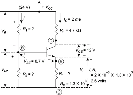
FIGURE 4.18 Design of potential divider bias circuit
Solution Since stability factor S = 5 and β = 50
![]() Can be calculated using the expression for S from equation 4.22.
Can be calculated using the expression for S from equation 4.22.

RE can be calculated from the expression

Substituting the value of RE = 1.3 KΩ, S = 5; β = 50 in the equation (4.27)
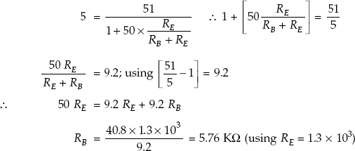
From the circuit

Thermal Runaway and Thermal Stability
In a CE transistor IC = βIB + (β + 1) ICO (4.29)
ICO is reverse current through the base-collector junction, which is reverse biased for active region operation (IC0 doubles for every 10°C rise in temperature). Since ICO is temperature dependent, Ic increases with increase in temperature. The increase in collector current IC increases the power dissipation at collector-junction. This increases the junction temperature causing further rise in collector current. This process becomes cumulative and if proper care is not taken; the transistor gets destroyed, if the transistor ratings of maximum power dissipation are exceeded. The maximum average power dissipation PCmax specified by the transistor manufacturers should not be exceeded for its specific application.
This cumulative process or the phenomenon due to self-heating, in which rise in temperature and current chase each other resulting in increased power dissipation PC, is called thermal runaway and can be prevented by proper biasing for low power circuits and by using heat sinks for transistors operating at large powers.
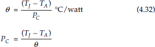
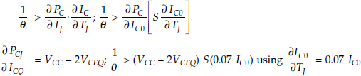
Before proceeding further, some criteria have to be defined. In this context a term called thermal resistance θ is defined below.
The power dissipation PC in watts at the collector junction is proportional to variations in temperature at the collector junction with reference to ambient temperature i.e. (TJ – TA). The temperature rise at the collector junction is proportional to the power dissipation at the junction.
where, TJ = junction temperature in °C
TA = ambient temperature in °C
The proportionality between Pc and (TJ – TA) can be converted into an equality by introducing a constant θ so that
where, θ is called the thermal resistance and has a dimension of temperature in °C per watt of power dissipation. The size of the transistor and the device heat transfer methods to surroundings determine the magnitudes of thermal resistance.
Differentiating with respect to
This gives the relation between the thermal conductivity and power dissipation change dPC with respect to junction temperature change dTj.
As long as

This condition must be satisfied to prevent thermal runaway and to safe guard the device.
If thermal conductivity is more than the rate of power dissipation with respect to temperature, thermal runaway is prevented. This can be justified as follows, more thermal conductivity means carrying away the heat from the transistor junction into the surroundings as quickly as is generated. As long as the heat is radiated away, thermal runaway is prevented. If it is not possible to directly radiate away heat by having proper ventilation; special heat sinks, which carry away the heat have to be designed.
In one configuration the device is enclosed (embedded) in the heat sink. Other configurations of heat sink designs are also possible for example in power transistors. The collector is connected to the case of the transistor, and can be fixed on a heat sink insulated from the ground.
In low power devices, thermal runaway can be prevented by careful selection of the quiescent or D.C. operating point. The power generated at the collector junction PCJ under no excitation signal condition is the product of ICQ and VCEQ
where VCEQ = VCC − ICQ.(RL + RE)
∴ PCJ = VC.EQ × ICQ (4.35)
Also, PCJ = VccICQ − I2CQ(RL + RE) (4.36)
where VCC.ICQ is the D.C. power supplied by the D.C. source VCC. A part of this power is consumed as power dissipation PdC in the resistors RL and RE.
from equation (4.29), the condition to prevent thermal runaway is
But
And ![]() is 7% per °C. This is because ICO doubles for every 10 °C rise in temperature or in other words, ICO changes by 7% per °C for both silicon and germanium transistors.
is 7% per °C. This is because ICO doubles for every 10 °C rise in temperature or in other words, ICO changes by 7% per °C for both silicon and germanium transistors.
That is, ![]()
Therefore, it can be written that
This condition can be applied to the equation for the power
Differentiating PCJ with respect to ICQ
[For class A amplifier with RL, the resistive load VCEQ = ICQ (RL + RE)]
For class A amplifier with resistive load, ![]()
∴ VCEQ = 2.VCEQ − ICQ (RL + RE) and therefore, VCEQ = ICQ (RL + RE)}
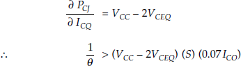
For this inequality to be satisfied, it requires that VCC – 2VCEQ is positive so that ![]() . This is the biasing condition requirement to avoid thermal runaway. That is, the operating point is not chosen at
. This is the biasing condition requirement to avoid thermal runaway. That is, the operating point is not chosen at ![]() ; but such that
; but such that ![]() . This, of course, reduces the possible signal swing and the circuit is under utilised; but this ensures safety against thermal runaway.
. This, of course, reduces the possible signal swing and the circuit is under utilised; but this ensures safety against thermal runaway.
However, when high power transistors are involved, this simple manipulation does not work and design of proper heat sinks becomes a must.
4.5 Small Signal Low Frequency Amplifier
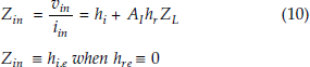
An amplifier can be considered as a two-port (four-terminal) network, with conveniently defined parameters, which find practical use. For instance, for a transistor, the hybrid parameters are useful for the design of transistor circuits. Transistor is basically a current amplifier but natural sources are voltage type in nature. So, the following expressions are used to represent the input and output relations.
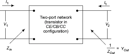
FIGURE 4.19 Transistor as two-port network
Considering the transistor as shown in the Fig. 4.19
Putting the above equations in matrix form
As can be seen later, the parameters h11, h12, h21 and h22 do not contain same units; h-parameters are known as hybrid parameters.
From the above equation, by applying some boundary conditions, h-parameters can be obtained. If in equation (4.40) and (4.41), V2 is made zero, that is, output port is short-circuited.
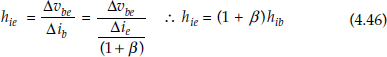
h11 has the dimensions of a resistance and pertains to the input port and it can be termed input resistance hi represented by ![]() The unit of input resistance hi is ohms.
The unit of input resistance hi is ohms.
In the same way, ![]()
h21 is a dimensionless quantity representing the ratio of output current to input current or current gain. This is represented by ![]() and is called forward current gain hf. It is a dimensionless quantity.
and is called forward current gain hf. It is a dimensionless quantity.
Now, by making I 1 = 0 or open circuiting the input port; two more parameters are obtained as following.
h12 is a reverse voltage transfer ratio and is named hr. It is a dimensionless quantity and gives an idea as to the voltage that appears across the input port. This in fact, represents the unwanted voltage transfer from the output to the input, since amplifiers should be preferably unilateral in transfer of energy from input into the output ports, but not the other way round.
Finally, ![]()
h22 represents the admittance of the output port and is designated as output conductance, ho. ho is measured in mhos or Siemens.
Thus, as the h-parameters possess a mixture of units, and hence are known as hybrid parameters.
When applied to analysis of amplifiers with alternating signals V2 = 0 and I1 = 0 represent constant D.C. values of voltage at the output port and current at the input port. Since the transistor characteristics are not entirely linear, the values of the h-parameters change from point to point and are defined over small linearised regions and hence are called small signal parameters.
In this context, input resistance
Forward current gain
Reverse voltage transfer ratio
Output conductance
Transistor amplifiers can have three configurations with any one of the terminals grounded. The other two terminals forming the input and output terminals subjected to the original definition.
So, three sets of h-parameters are obtained with the second subscript to the h-parameters, designating the grounded terminal.
So for CE configuration of transistor, the h-parameters become hie; hfe; hre and hoe.
For common base transistor configuration, these parameters are hib; hfb; hrb and hob.
For common collector transistor configuration, the h-parameters are hic; hfc; hrc and hoc.
All these parameters can be determined from the static characteristics of the transistor as described in the device chapter.
The different sets of parameters are inter related and inter convertible.
For instance,
or,
Similarly,
or,
For common collector parameters; ![]()
∴ hfc = (1 + hfe) or (1 + β) (4.48)
hic and hoc are equal to hie and hoe, respectively.
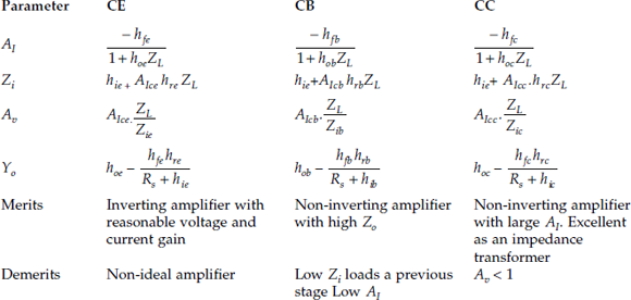
Comparison of CE, CB, CC Configurations of Transistors Between CE, CC and CB transistor configurations as per chosen directions of positive and negative polarities, CE transistor configuration is considered to be an inverting voltage amplifier, whereas for the same chosen polarities, CB and CC configurations form non-inverting amplifiers.
Common emitter transistor configuration has input impedance hie of the order of 1 K Ohm and output impedance ![]() is of the order of 40 K ohms.
is of the order of 40 K ohms.
For common base configuration the input impedance hib will be of the order of a few ohms 10 to 20 ohms and has output impedance ![]() of the order of 2 M Ohms.
of the order of 2 M Ohms.
CB transistor configuration has a reasonable voltage gain but current gain hfb or α is less than unity. (IC (output current) < IE (input current)).
Common collector transistor configuration (CC) has a current gain of hfc = (1 + hfe) but the voltage gain is less than unity (as will be explained later it forms the voltage series negative feedback amplifier with feedback factor ![]() = 1).
= 1).
Common emitter (CE) transistor amplifier is neither a true current amplifier nor a voltage amplifier, but a bit of both.
Common base transistor amplifier is an almost ideal current controlled current generator, since its input impedance is low and can be connected to a current source. Since its output impedance is high it can act as a current source, that is, in effect a current controlled current source.
CC configuration due to unity feedback factor has very high input impedance and very low output impedance and can act as a voltage controlled voltage source.
Although the active devices BJTs and FETs have different bases of physical operation, once their circuit models replace these devices, their frequency response and other features can be analysed simultaneously. The following h-parameter model is for bipolar junction transistors.
Analysis of Amplifiers using h-Parameter Models
Just like equations can be framed for circuits, circuits can be formed from equations. Considering the equations
Vin = hi.iin + hr.Vout
Iout = hf.iin + h0.Vout (4.49)
The following circuit of Fig. 4.20 can be shown with the h-parameters representing the above equations
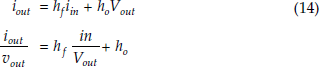
When ZL is connected across the output port, a current IL flows in ZL. Therefore.
The current gain Ai is by definition

FIGURE 4.20 Small signal low frequency transistor equivalent circuit using h-parameters
From the circuit of Fig. 4.20; iout = hfiin + ho(– ioutZL)

From the equation (4.49)

But Vout = − iout ZL (4.55)
![]()
Since
![]()
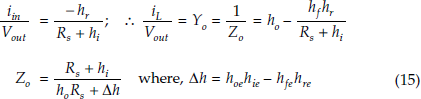
The input impedance,
![]()
AV. the voltage gain by definition is equal to
From the Fig. 4.18; Vout = – Iout ZL
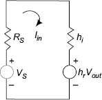
FIGURE 4.21 Equivalent circuit at input port (of CE Transistor) with signal source VS.
To find Zo which is defined as
Dividing throughout by Vout
From Fig. 4.21 with VS = O;hr Vout = − (Rs + hi) × Iin

The amplifier performance can be completely assessed by the four basic relations for AI, AV, ZI and Zout obtained previously. The expressions for these relations together with comparison are summarised in the following Table.
Typical values of transistor h-parameters are as follows:
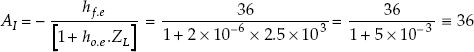
Example 1 Find the values of AI; Av, AVS, AIS; Zi; & Zo for the following circuit.
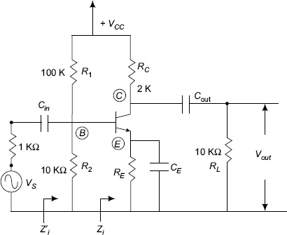
FIGURE 4.22 Common emitter transistor amplifier circuit
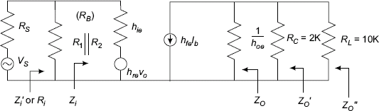
FIGURE 4.23 Small signal low frequency equivalent circuit using h-parameters
hfe = + 50; hie = 1 K Ω; hre = 4 × 10⁻⁴; hoe = 25 × 10–6 mhos
Since RC = 2 KΩ and RL = 10 KΩ
The effective load ZL for amplifier = ![]()
Avs refers to voltage gain taking the signal source resistance Rs into consideration
AIs refers to current gain taking RS into consideration.
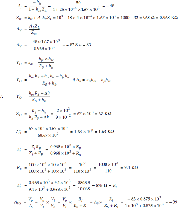
Example 2 Find all the following quantities AI; Zi; AV and ZO for the following common base transistor amplifier. hfb = – 0.99; hib = 20Ω hrb = 2 × 10⁻⁴ hob = 0.5 × 10⁻⁶ Siemens.
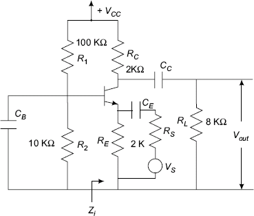
FIGURE 4.24 Common base transistor amplifier

FIGURE 4.25 A.C. equivalent circuit

FIGURE 4.26 A.C. equivalent circuit with h-parameters
h0b. Z′L = 0.5 × 10–6 × 1.6 × 103 = 8 × 10⁻⁴
1 + h0b. Z′L = 1 + 8 × 10–4 = 1.0008
Current Gain ![]()

From the above calculations for the common base transistor amplifier, the amplifier gain is less than one. The input impedance Zin is only a few ohms and the output impedance Zout is very high and is of the order of megaohms. The reasons for such behaviour of common base amplifiers are well discussed in discussing the common base transistor characteristics. Common base transistor amplifier is a non-inverting amplifier.
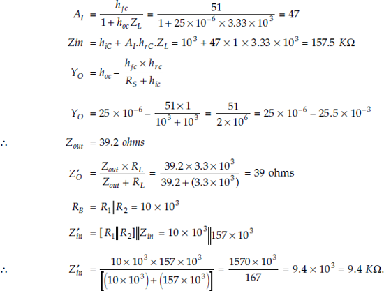
Example 3 Find AI, Zi, AV, and Zo for the following common collector amplifier circut. Data: RS = 1 Kohms, ZL = 3.3 Kohms; hfc = 51; h0C = 25 × 10–6; hrC = 1 and hiC = 1 Kohms
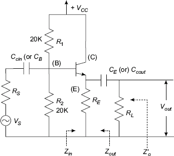
FIGURE 4.27 Common collector transistor amplifier

FIGURE 4.28 Equivalent circuit
Small Signal Low Frequency Model for a Common Emitter Transistor Amplifier
In the following circuit R1 and R2, VCC; RE and RC provide forward bias to emitter junction and reverse bias to collector junction of the transistor to keep the transistor in the active region. RE provides bias stabilization. RC forms the D.C. load. The collector supply voltage VCC, RC and RE are so chosen to keep the operating point for class A operation.
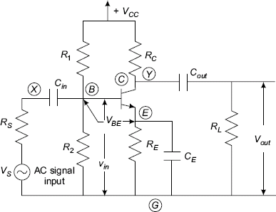
FIGURE 4.29 Common emitter transistor amplifier circuit
Mostly, voltage amplifiers are CE type and use resistive loads and operate under class A condition. The input impedance for various values of load resistances and the output impedance for various values of source resistance for CE transistor operation will be fairly constant. CE transistor amplifier configuration is normally preferred.
Between base and emitter; voltage across R2 and voltage across RE are such that VBE = VR2 – VRE For an N-P-N transistor, VR2 > VRE to satisfy the forward bias condition, that is, base should be more positive with respect to the emitter
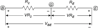
FIGURE 4.30 VBE for the emitter junction
VBE forward biases the base to emitter junction of the transistor. Input signal Vs is an alternating signal source in nature that is connected to the input port of the amplifier. Input signal Vs is coupled to the base through a coupling capacitor CCin or Cin or CC or Cb. Thus, the capacitor Cin blocks the D.C. bias VBE from entering the signal source; but allows A.C. signal into the input port. XCc iput should be as small as possible compared to Zin and if this is not possible Zin should be at least 10 times larger than ![]()
Instantaneous voltage,
neglecting the source resistance RS. The above equation requires that XCin → zero; Then, maximum voltage will be available between base and the emitter. The series coupling capacitors are so selected as to act as short circuits to A.C. signals, while they act as open circuit for D.C. biasing voltages (of individual stages to be adjusted independently in cascaded amplifiers). Capacitor CE across RE should have a reactance less than ![]() of the magnitude of RE at the lowest frequency of the signal base band to be amplified. This is justified since; the reactance is maximum at the lowest frequency and decreases with increasing frequency.
of the magnitude of RE at the lowest frequency of the signal base band to be amplified. This is justified since; the reactance is maximum at the lowest frequency and decreases with increasing frequency. ![]() Once it is an effective short circuit at lowest frequency of the signal to be amplified, it is more effective short circuit at all higher frequencies. CE keeps the emitter grounded (for common emitter transistor configuration) for A.C. signals. Similarly, Cout or CCout or Cb or CC should become perfect short circuits for A.C. signals and perfect blocks for D.C.; so that A.C. and D.C. voltages are well separated.
Once it is an effective short circuit at lowest frequency of the signal to be amplified, it is more effective short circuit at all higher frequencies. CE keeps the emitter grounded (for common emitter transistor configuration) for A.C. signals. Similarly, Cout or CCout or Cb or CC should become perfect short circuits for A.C. signals and perfect blocks for D.C.; so that A.C. and D.C. voltages are well separated.
Now, the A.C. input signal Vin is super imposed on the D.C. bias VBE and the instantaneous voltage Vbe will be
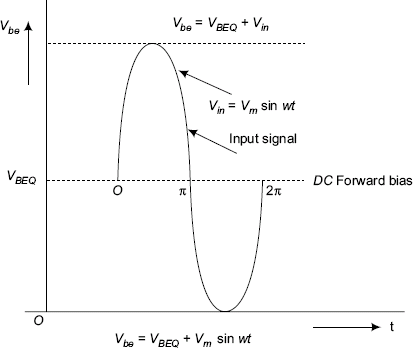
FIGURE 4.31 Effective voltage Vbe between base and emitter
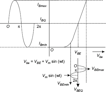
FIGURE 4.32 Input signal variations about the forward bias VBEQ
where Vbe is effective changing D.C. between base and the emitter. This causes the base current to vary sinusoidally and the collector current likewise varies from its quiescent value between ICQ – ICmin and ICmax – ICQ. This varying collector current develops a voltage across the resistance RC that again varies between VC max and VC min. To avoid notational ambiguity the following quantities are defined below.
Vbe varying voltage between B and E is the sum of D.C. bias VBE and instantaneous value of the super imposed A.C. signal Vm sin ωt.
Vbe = instantaneous value of the superimposed signal
VBE the operating quiescent bias between B and E, VR2 – VE = VBE.
Since the output required is A.C. it is developed across RC. Due to this presence of RL the effective load resistance R’L becomes RL║RC for the purposes of calculation of gain and so on.
Though it is convenient for analysis to consider C → ∝; no more than the value needed to make ![]() are used.
are used.
Otherwise, the initial charging current of the capacitance may exceed the maximum rated current of the device and the device blows of.
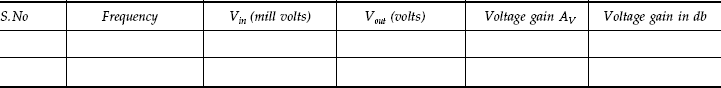
Determination of frequency response of a common emitter transistor amplifier To determine the frequency response of an amplifier a function generator (signal generator) is connected to the input terminals of the amplifier. The input signal is also connected to channel one of a CRO to measure the input signal amplitude Vin and observe the wave form. The output signal obtained at the output port is connected to the second channel of the CRO to measure the amplitude Vout and to observe the waveform of output signal. The voltage gain AV of the amplifier is ![]() ; and Voltage gain in db = 20 log10
; and Voltage gain in db = 20 log10 ![]() . The magnitude of Vin is maintained constant and by changing the frequency of the input signal in convenient steps; the output voltage Vout is measured. The results are tabulated as following
. The magnitude of Vin is maintained constant and by changing the frequency of the input signal in convenient steps; the output voltage Vout is measured. The results are tabulated as following
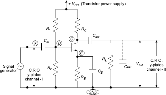
FIGURE 4.33 Experimental setup for obtaining frequency response of CE amplifier.
Frequency response of the amplifier is plotted on a semi-Log graph sheet with the X-axis representing logarithm of frequency and on the Y-axis voltage gains AV

FIGURE 4.34 Frequency response of an amplifier
It will be observed from the frequency response plot of the amplifier that starting from D.C. frequency; the gain increases with frequency (low frequency region) and enters the knee region, remains almost flat over a range of frequencies (midrange frequencies) and starts falling off with frequency at high frequency region.
The response of the human ears is logarithmic in nature. (For this reason only decibel (db) gain is defined). Even if power of the signal reaching the human ear is reduced to half, it feels only a slight difference in amplification. Between these two power levels, the human ear cannot differentiate (3-db). So, between the two frequencies f1 (fL) and f2 (fh): the power is at least half of the maximum power. These two frequencies and the range between them (f2 – f 1) or (fh – fL) is called as bandwidth (B.W) of the amplifier. Between these two cut-off frequencies or corner frequencies the response of the amplifier is considered to be uniform.
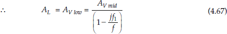
In voltage relationships; the 3-db point refers to ![]() of AV mid (0.707 Amid) where, AVmid is the maximum gain AVmax in the flat region of the response characteristic. This flat response region is known as midfrequency region of the amplifier response.
of AV mid (0.707 Amid) where, AVmid is the maximum gain AVmax in the flat region of the response characteristic. This flat response region is known as midfrequency region of the amplifier response.
Reasons for fall of gain at low frequency (the combined effect of Cin, CE and Cout).
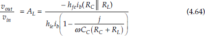
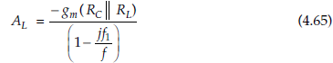
As the frequency increases, reactance of these capacitances decrease and in the flat region and beyond, they are virtual short circuits. Up to the flat frequency region the equivalent of a CE amplifier acts as a high pass filter with f1 as cut-off frequency, since high pass filter has stop band region up to f1, beyond which it has the pass band.
Reason for Fall of Response at High Frequencies. RL is the load resistance in the circuit of the appliance connected to the amplifier, which is to receive only the A.C. output from the amplifier. Every appliance will have two terminals with a potential difference across them and so possesses a capacitance. This is represented as a capacitance Csh, across the resistance RL.RL together with the capacitance across it could be the input impedance shunted by its input capacitance of a two-port network connected across the output terminals of the amplifier. This represents a low pass filter with a cut-off frequency of fh or f2 and up to f2 it is the pass band and beyond which it has stop band, that is, up to f2, all higher frequencies.
C E Amplifier Equivalent Circuits for Mid-frequency, Low Frequency and High Frequency
The exact equivalent circuit for a simplified common emitter model (hre = hoe = 0) is shown in the following Fig. 4.35.
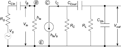
FIGURE 4.35 C E transistor amplifier equivalent circuit
At mid-frequencies, the circuit is redrawn as follows, since the series capacitances are short circuits and the shunt capacitance is open circuit. Mid-frequency equivalent circuit is in Fig. 4.36,
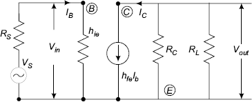
FIGURE 4.36 C E transistor amplifier mid-frequency equivalent circuit
Low Frequency Equivalent Circuit The circuit of Fig. 4.37 can be redrawn as shown in Fig. 4.38
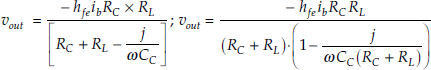
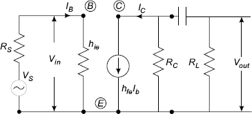
FIGURE 4.37 C E transistor amplifier low frequency equivalent circuit

FIGURE 4.38 C E transistor amplifier low frequency equivalent circuit
where,
From this equation, it is found that at frequency f = f1
Thus, f1 is the lower half-power frequency or low frequency Cut-off point.
High frequency equivalent circuit
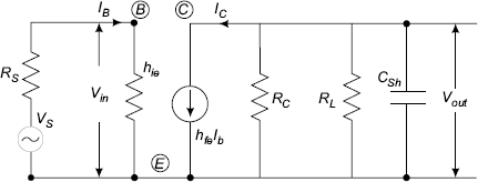
FIGURE 4.39 High frequency equivalent circuit of CE transistor amplifier
The circuit in Fig. 4.39 is redrawn as shown in the Fig. 4.40.
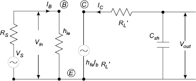
FIGURE 4.40 High frequency equivalent circuit of CE transistor amplifier
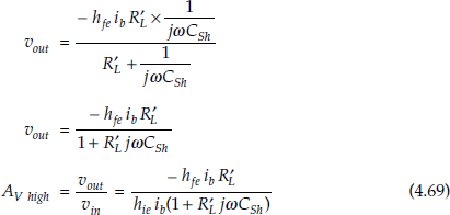
where
at
So, f2 is the upper half power frequency. And, the bandwidth (B.W.) is (f2 – f1) but f1 << f2 so bandwidth ≅ f2. f1 is dependent on the series combination of RC and RL together with CC.f2 is dependent on the parallel combination of RC and RL together with CSh.
In the first case, if CC becomes large; f1 will be reduced while if CSh is large, f2 will be reduced. Larger the value of CC smaller is f1 and smaller the value of CSh; larger is the f2. So, for maximum bandwidth CC should be as large as possible and CSh should be made as small as possible.
4.6 Emitter Follower
Emitter follower is another form for a common collector amplifier, since the collector is at A.C. ground as can seen from the circuit of Fig. 4.41. The name emitter follower arrives from the fact that the output voltage across the resistor RE in the emitter circuit is almost equal to or slightly less than input base-ground voltage (i.e. base-collector voltage). (Emitter voltage follows the changes in input signal voltage). The characteristic features of emitter follower are as following. The voltage gain is less than unity with no phase inversion between the input and the output signals. It has a high input impedance and low output impedance making it an ideal voltage controlled voltage source and is commonly used for impedance transformation over a wide range of frequencies. The circuit has relatively high current gain and power gain.
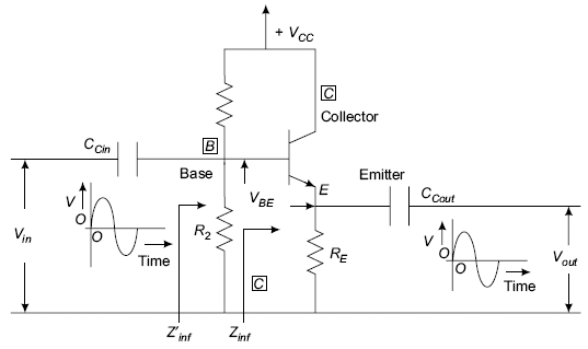
FIGURE 4.41 Emitter follower (common collector amplifier)
h-Parameter Model A.C. Equivalent Circuit of Emitter Follower
h-parameter model A.C. equivalent circuit of emitter follower is drawn with an assumption that hre = hoe ≅ 0 so that ![]() = ∞. That is, an open circuit and so the circuit component
= ∞. That is, an open circuit and so the circuit component ![]() parallel to the output current source is omitted in the equivalent circuit of Fig. 4.42. Further, in the following analysis, the effect of R1 and R2 is not considered. The effect of R1 and R2 is to reduce the input impedance Zif to Zif because of the effect of R1 and R 2′
parallel to the output current source is omitted in the equivalent circuit of Fig. 4.42. Further, in the following analysis, the effect of R1 and R2 is not considered. The effect of R1 and R2 is to reduce the input impedance Zif to Zif because of the effect of R1 and R 2′

FIGURE 4.42 h-parameter model A.C. equivalent circuit for emitter follower (common collector amplifier)
The input impedance Zin has been enhanced by an amount [(1 + hfe).RE]
Vin = hie.IB + (1 + hfe).IB.RE
But, Vout = IE.RE = (1 + hfe).IB.RE
∴ Voltage Gain

Output impedance Z0 across the output terminals is by definition Z0 = ![]() ; where, V is the open circuit voltage across the output terminals and I is the short circuit current. When the emitter is open, the open circuit voltage V0 is Vin = IB.hie. The short circuit current ISC = IE and ISC = IE and ISC = IE = (1 + hfe).IB
; where, V is the open circuit voltage across the output terminals and I is the short circuit current. When the emitter is open, the open circuit voltage V0 is Vin = IB.hie. The short circuit current ISC = IE and ISC = IE and ISC = IE = (1 + hfe).IB
![]()
Then, the output impedance Z0 is ![]() , a low value when compared to the input impedance Zin where, ⌊ hie + (1 + hfe).RE⌋ which is relatively very large.
, a low value when compared to the input impedance Zin where, ⌊ hie + (1 + hfe).RE⌋ which is relatively very large.
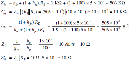
Example on emitter follower circuit For the following emitter follower circuit of Fig. 4.43; R1 = R2 = 20 KΩ; hie = 1 KΩ; hfe = 100; RE = 5 KΩ, neglect the effect of hoe. Determine the input impedance Zin; Z′in; output impedance Z0 and Z’0 and voltage gain AV.
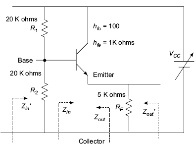
FIGURE 4.43 Emitter follower circuit
4.7 Junction Field Effect Transistor (JFET) Amplifiers
To provide the necessary negative voltage VGS, better biasing scheme is voltage divider biasing, where R1 and R2 form a voltage divider together with RS and the supply voltage VDD provides a negative voltage at the gate of the JFET device as shown in the Fig. 4.44.
For a specified Q point of JFET amplifier circuit (ID, VGS) and chosen values of VGN and RG, the required values of R2; R1 and RS are easily calculated from

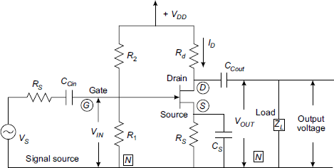
FIGURE 4.44 Common source JFET amplifier circuit
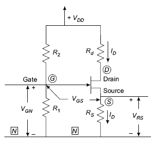
FIGURE 4.45 D.C. equivalent circuit of common source JFET amplifier circuit
Furthermore, the effect of any shift in VGS is reduced by making | VSN | large compared to | VGS |.
Example The JFET is to be operated at a quiescent point defined by ID = 4 mA. VDS = 8 V and VGS = – 2 V. Design an appropriate biasing circuit with VDD = 30 volts.
Solution Using the voltage divider bias circuit, assume VGN = + 12 volts, so that VGN – VGS = VSN is large compared to VGS for stability. That is, the effect of any shift in VGS is reduced.
Assume RG = 6 M Ω to keep the input resistance high.
Then, VSN = IDRS = VGN – VGS = 12 – (– 2) = 14 volts
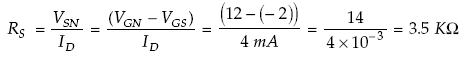

FIGURE 4.46 D.C. equivalent circuit of common source JFET amplifier circuit
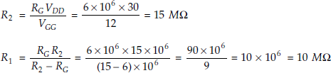
Summing voltages around the drain loop yields ∑V = 0 i.e.VDD – ID.RD – VDS – IDRS = 0
For VDS = 8 volts (from the data of the given Q point (Quiescent operating point))
Thus, the magnitudes of component values of R1; R2; RS and RD are estimated based on the given data of the D.C. equivalent circuit of common source JFET amplifier.
Small signal low frequency model of a FET device A small signal to an amplifier input is one to which a given device responds in a linear fashion. The following equivalent circuits are discussed for small signal low frequency operation of the FET amplifier. During the discussions on the characteristics of the FET devices, the significance of drain resistance rd as the device internal resistance and transconductance gm from the transfer characteristics of the device are clearly explained
The FET device parameters gm, rd and μ allow an A.C. equivalent circuit for field effect transistor (FET) just like a BJT.
In the Fig. 4.47 irrespective of the configuration common source, common gate and common drain amplifier (similar to h-parameter equivalent circuit for CE, CB and CC configurations of BJT), the active device FET can be represented by a derived voltage source μVGS with the shown polarity between source and drain in series with the drain resistance rd.
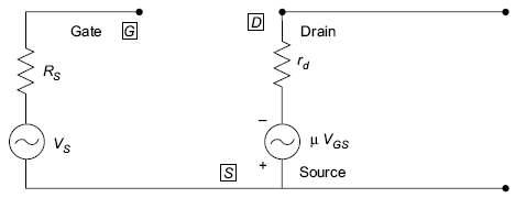
FIGURE 4.47 Equivalent circuit of a field effect transistor (FET)
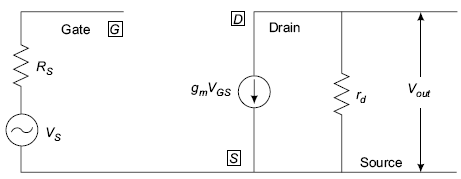
FIGURE 4.48 Equivalent circuit of a field effect transistor (FET)
Alternate representation for FET amplifier equivalent circuit is shown in Fig. 4.48.
Common Source FET Amplifier
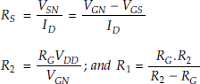
In the Fig. 4.49, VDD, RS – CS, RG and RD provide the required biasing voltages to the FET device for the required class of operation of the amplifier and in this case for a linear amplifier, class A amplifier for small signal and low frequency operation. The input signal voltage V in is applied between the gate and the source. The A.C. signal output voltage V0 is developed across the drain circuit resistance RD. CCout is the blocking capacitor, which blocks the D.C. from the drain to source of the FET to the output load or next stage of amplifier as the case may be and also acts as the coupling capacitor that couples or allows A.C. output signal voltage to the load. On similar lines, CCin has dual roles of acting as a blocking capacitor, which prevents the D.C. from entering the driving source, and couples the input signal voltage to the input port between the gate and source of the FET device. RG is the gate leak resistance or gate resistor to provide high input impedance as well as a leakage path for the capacitance to discharge. RG also provides the connecting path for the D.C. bias developed across the source resistance RS to be applied to the input terminal, the gate. RS provides the necessary bias and CS provides bypass path for A.C. signals (around RS) to make the source at the ground potential (and also eliminates feedback to the input port), justifying the common source configuration or common source operation of the FET amplifier as shown in Fig. 4.50.
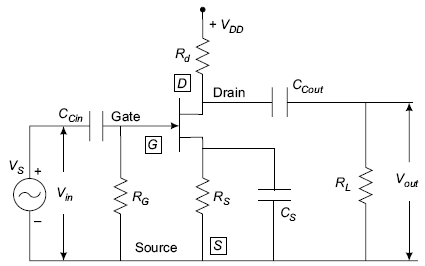
FIGURE 4.49 Common source FET amplifier
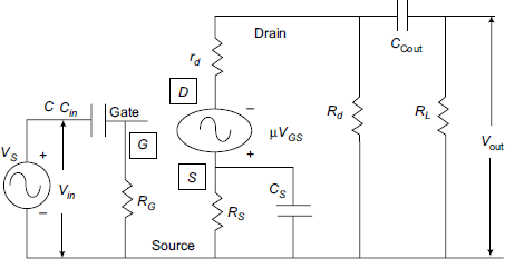
FIGURE 4.50 Small signal low frequency equivalent circuit of common source FET amplifier
The above circuit shown in the Fig. 4.50 is the small signal low frequency A.C. equivalent circuit of a common source FET amplifier. The following rules have to be followed while drawing the A.C. equivalent circuit:
- The FET device is replaced by a controlled voltage source of μVGS with the indicated polarity in series with the drain resistance rd between the source and the drain terminals. The gate terminal is left free and can be connected to points depending on the actual components in the circuit.
- No other component can be replaced and they have to be represented in tact depending upon the actual circuit.
Thus, for the actual common source FET amplifier circuit of Fig. 4.49, the A.C. equivalent circuit is shown in Fig. 4.50.
At above the frequencies when XCci << RG and XCco << RL and XCs << RS, the above circuit gets simplified as shown below in Fig. 4.51.
The voltage gain AV; Zin and Zout can be calculated using the conventional network methods. By inspection of the equivalent circuit in Fig. 4.50, it can be seen that VGS = VS at the input port of the amplifier. In the output port applying Kirchoff’s Voltage Law to the loop SDS from the source to drain and then back to source.
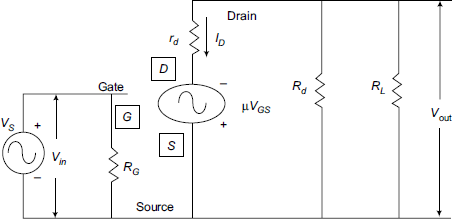
FIGURE 4.51 Small signal low frequency simplified equivalent circuit of common source FET amplifier
μ.VS + ID.rd + ID.Rd||RL = 0
or,
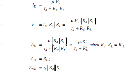
An alternate approach is to replace the FET by its Norton’s equivalent circuit as shown in the following Fig. 4.52.
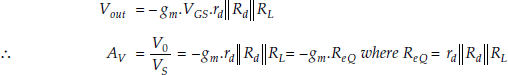
The input impedance Zin = RG and Zout = ReQ = rd ║ Rd ║ RL
Thus, the input impedance and the output impedances remain the same.
For maximum voltage gain AV it requires that rd << Rd║ RL. Then, the maximum value of the voltage gain will be approximately equal to μ.
This is the maximum theoretical gain one can ever realise from the FET amplifier circuits.
The common source mode FET amplifier is the most popular circuit in applications.
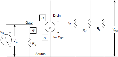
FIGURE 4.52 Small signal low frequency alternate equivalent circuit of common source FET amplifier
Common Gate FET Amplifier Circuit
The following is the circuit of a common gate amplifier. The gate is grounded and the driving signal source is connected in the source lead terminal. The load resistance Rd in the drain path and the external load resistance RL are connected between the drain and the gate electrodes as shown in the following Fig. 4.53

FIGURE 4.53 Common gate FET amplifier circuit
Common gate FET amplifier circuit with self-bias arrangement is shown in the Fig. 4.54.
When CCin = CCout = CS are all so large as to make their reactances negligible compared to the resistances Rin, Rout and Rs the following equivalent circuit in Fig. 4.54 is drawn.
From the equivalent circuit of Fig. 4.55, it is clear that VGS = VS.
On the loop DSGD in the Fig. 4.55,
–Vs + μ.VGS + ID (Rd + rd) = 0
But VGS = –VS
∴ –Vs – μ.VS + ID. (Rd + rd) = 0

FIGURE 4.54 Common Gate amplifier with self bias
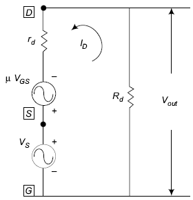
FIGURE 4.55 Common gate FET amplifier equivalent circuit

But,
∴ Voltage Gain
The voltage gain AV is almost the same as for common source model FET amplifier with no inversion between the input and the output voltages. Thus, this common gate amplifier is a non-inverting amplifier with a gain derived as
But the input impedance Zin of the common gate amplifier will be very low as seen from the following equation
If rd >> Rd, then
4.8 Common Drain FET Amplifier (Source Follower)
When the drain terminal is common to both the input port and the output port of the FET amplifier, the circuit is called as common drain FET amplifier or the source follower.
The source follower just like the emitter follower is an impedance matching network. It provides a low output impedance so as to make this an almost ideal voltage source. Thus, the total amplifier works as an ideal voltage controlled voltage source.
The common drain FET amplifier has the input voltage VIN between gate and the common drain and the output voltage VOUT is available between the source and the common drain terminals of the FET device. The output voltage is developed due to the flow of the drain current Id through RS. Therefore, VS = Id. RS. The output voltage and the input voltages will be in phase, which can be seen from the directions and polarities of the input signal voltage and the output voltages. The output voltage VOUT at the source terminal (source voltage) follows the input signal changes at the gate terminal of the amplifier. So, this common drain amplifier circuit is also known as source follower circuit. Since the output voltage of the source follower circuit is almost equal to the input voltage, the gain of the source follower is approximately unity.
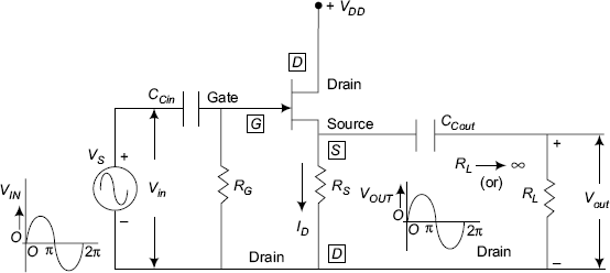
FIGURE 4.56 Common drain FET amplifier (source follower)

FIGURE 4.57 Common drain FET amplifier equivalent circuit
From Fig. 4.57 VGS = Vin – ID·RS and also
−μ.VGS + (rd + RS).ID = 0
∴ −μ(Vin − ID.RS) + (rd + RS).ID = 0
−μ.Vin + ID[(rd + RS(μ + 1)] = 0
or,
Output voltage

FIGURE 4.58 Common drain FET amplifier equivalent circuit (redrawn from Fig. 4.57)
Vout can be written as Vout = 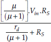
∴ Voltage Gain
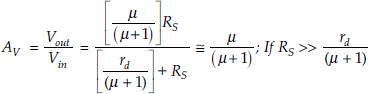
Also, Voltage Gain
∴ Voltage Gain
Therefore, the voltage gain, AV of a common drain FET amplifier is close to unity, similar to the emitter follower circuit.
From the equation ID = 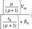 we can draw a circuit as shown in the Fig. 4.59.
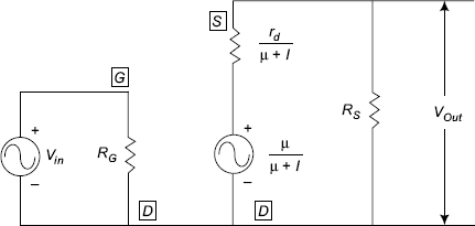
FIGURE 4.59 Common drain FET amplifier equivalent circuit
The circuit represents a controlled source with voltage ![]() in series with an impedance
in series with an impedance ![]() driving a load resistance RS.
driving a load resistance RS.
Thus, the controlled source impedance or the so-called output impedance Zout or the output resistance Rout of the source follower is ![]()
It is interesting to note that the output impedance of the source follower is the same as the input impedance of the common collector transistor amplifier (emitter follower) that is ![]() .
.
Thus, the source follower acts as a unity voltage gain non-inverting amplifier with a very low source impedance of ![]() of or acts as an ideal voltage controlled voltage source. Further, it has got
of or acts as an ideal voltage controlled voltage source. Further, it has got
large bandwidth to have good frequency response (from the concept of the product of gain and bandwidth of amplifiers is constant) and stable operation due to inherent negative feedback in the amplifier operation.
Further, the high input impedance Zin of the source follower circuit is used in measuring instruments when loading on the input signal sources is to be minimised. One of the applications is at the input stages of amplifiers used in cathode ray oscilloscopes.
Unity gain of the source follower and impedance transformation feature, that is, the very low output impedance ZOUT and high input impedance ZIN feature of the source follower circuit is used as Unity Gain Buffer Amplifier in instrumentation circuits.
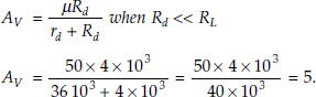
Example A common source FET amplifier has rd = 36 KΩ; μ = 50; Rd = 4 KΩ. Calculate the voltage gain AV using the given data for the common source FET amplifier.
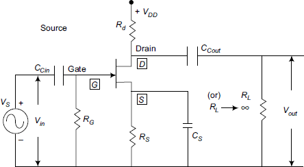
FIGURE 4.60 Common sourrce FET amplifier
Solution
Voltage Gain
Example For a common gate FET amplifier circuit, μ = 50, Rd = 2 KΩ and rd = 38 KΩ, calculate the voltage gain AV.
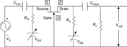
FIGURE 4.61 Common gate FET amplifier circuit
Solution The voltage gain of common gate FET amplifier AV
Example The common drain FET amplifier circuit is shown in the following Fig. 4.62. The FET device has μ = 50, rd = 46 KΩ; gm = 2 millimhos. RS = 4 KΩ and RG = 1 MΩ in the circuit. Calculate the voltage gain AV for the amplifier and the output resistance of the amplifier.
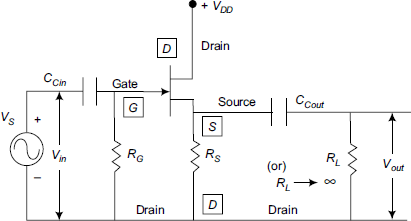
FIGURE 4.62 Common drain FET amplifier
Solution The voltage gain AV of the common drain FET amplifier circuit is given by the following expression,
Output resistance
Solved Examples
Example 1 Draw the circuit diagram of self-biasing circuit for a germanium transistor. Data: VCC = 20 V; RC = 2 K; RE =100 ohms. R1 = 100 KΩ; R2 = 5 KΩ; β = 50.

FIGURE 1 (Self bias circuit) Potential divider bias circuit
In the potential divider bias circuit of Fig. 1, VCC in association with R1 and R2 provide the bias and RE provides bias stability as is explained.
Determination of ICQ and VCE.Q and stability factor S
Solution
Stability factor
Voltage across ![]()
∴ voltage VRE across RE = VR2 – VBE = 0.95 – 0.3 = 0.65 V (using VBE = 0.3 V)
∴ ![]()
Collector to Emitter Voltage VCEQ = [VCC – IC.Q.(RC + RE)]
VC.E.Q = [20 – 6.5 × 10⁻³(2 × 10³ + 0.1 × 10³)] = [20 – 13.65] = 6.35 volts
Example 2 Discuss the concept of thermal runaway phenomenon in transistors
In a CE transistor IC = βIB + (β +1) ICO (1)
ICO is reverse current through the base-collector junction, which is reverse biased for active region operation (IC0 doubles for every 10°C rise in temperature). Since ICO is temperature dependent, Ic increases with increase in temperature. The increase in collector current IC increases the power dissipation at collector-junction. This increases the junction temperature causing further rise in collector current. This process becomes cumulative and if proper care is not taken; the transistor gets destroyed, if the transistor ratings of maximum power dissipation are exceeded. The maximum average power dissipation PCmax specified by the transistor manufacturers should not be exceeded for its specific application.
This cumulative process or the phenomenon due to self-heating, in which rise in temperature and current chase each other resulting in increased power dissipation PC, is called thermal runaway and can be prevented by proper biasing for low power circuits and by using heat sinks for transistors operating at large powers.
Example 3 Explain the phenomenon for thermal runaway.
The power dissipation PC in watts at the collector junction is proportional to variations in temperature at the collector junction with reference to ambient temperature, that is, (TJ – TA).
where, TJ = junction temperature °C in and TA = Ambient temperature in ° C.
The proportionality between Pc and (TJ – TA) can be converted into an equality by introducing a constant θ so that
where, θ is called the thermal resistance and has a dimension of temperature in °C per watt of power dissipation. The size of the transistor and the device heat transfer methods to surroundings determine the magnitudes of thermal resistance.
and,
Differentiating with respect to TJ;
This gives the relation between the thermal conductivity and power dissipation change dPC with respect to junction temperature change dTj as long as
This condition must be satisfied to prevent thermal runaway and to safe guard the device.
Example 4 Derive the condition for thermal stability.
For class A amplifier with resistive load, ![]()
∴ VCEQ = 2VCEQ − ICQ(RL + RE) and therefore, VCEQ = ICQ(RL + RE)
But, PCJ = VCCICQ − I2CQ (RL + RE)
Condition to avoid thermal runaway
For this inequality to be satisfied, it requires that VCC – 2VCEQ is positive so that VCEQ < ![]() . This is the biasing condition requirement to avoid thermal runaway. That is, the operating point is not chosen at VCEQ =
. This is the biasing condition requirement to avoid thermal runaway. That is, the operating point is not chosen at VCEQ = ![]() ; but such that VCEQ <
; but such that VCEQ < ![]() .
.
Example 5 Data: N-P-N transistor in CE mode. VCC = 10 volts. RC = 2 KΩ and RB. = 100 KΩ. Calculation of quiescent point and S for CE transistor with collector to base bias.

Stability Factor
Example 6 Mention the three methods of Biasing the CE transistor.
The three methods of biasing the transistors to fix up the quiescent operating point
(1) fixed bias or base bias circuit.
The choice of VCC; RL and RB is made such that forward bias VBE is provided to emitter junction and VCE provides the required reverse bias to the collector junction for the transistor to be operated as an amplifying device. In addition, VCC should always be less than VCE max, as prescribed by the specifications given by the manufacturer of the active devices.
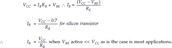
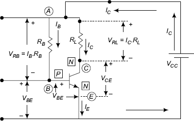
FIGURE 1 Fixed bias circuit for common emitter transistor
(2) collector to base bias circuit
In this circuit of Fig. 2, resistor RB is now connected between collector and base. It can be seen that stability of the quiescent operating point Q is improved. But this circuit is rarely used or obsolete now because of feedback through RB connecting the input and the output ports of the device. For the collector to base bias circuit in Fig. 2. (loop ACBEA)
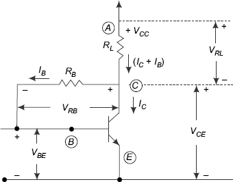
FIGURE 2 Collector to base bias circuit for N-P-N common emitter (CE) transistor
(3) Potential divider bias or voltage divider bias or self-bias circuit.
This potential divider bias circuit is now used in most of the applications as the circuit operation is more stable due to maintenance of stable quiescent operating by the Emitter resistor RE.
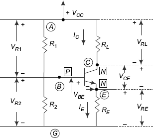
FIGURE 3 (Self-bias circuit) potential divider bias circuit
Example 7 Draw the circuit diagram of a common emitter transistor amplifier with self-biasing arrangement. Draw the h-parameter equivalent circuit of the amplifier. Derive the expressions for current gain AI; input resistance RIN; voltage gain AV and output resistance RO using the h-parameter equivalent circuit.
Solution Circuit diagram of a CE transistor amplifier circuit with self-bias is shown in Figure 1.
ANALYSIS OF AMPLIFIERS USING h-PARAMETER MODEL
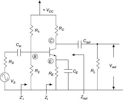
FIGURE 1 Common emitter transistor amplifier circuit
Just like equations can be framed for circuits, circuits can be formed from equations. Considering the equations
Vin = hi.iin + hr.Vout
Iout = hf.iin + h0.Vout (1)
The following circuit of Fig. 2 can be shown with the h-parameters representing the above equations
Derivations
When ZL is connected across the output port, a current IL flows in ZL. Therefore,
The current gain Ai is by definition
From the circuit of Fig. 2; iout = hf iin + ho (–ioutZL)

FIGURE 2 Small signal low frequency transistor equivalent circuit using h-parameters

From the equation (6)
But,

Since
The input impedance
Av the voltage gain by definition is equal to
From the Fig.
To find Zo which is defined as
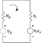
FIGURE 3 Equivalent circuit at input port (of CE transistor) with signal source VS
with VS = O, hrVout = − (Rs + hi) × iin (from figure 3)
Example 8 Calculate current gain; voltage gain; RN and ROUT using the following data
Data: hf.e = 36; RL = 2 × 10³ and ho.e = 2 × 10⁻⁶; hi.e = 1200 Ω. hr.e = 0. And RS = 500 Ω.
Solution Determination of current gain; AI
Determination of voltage gain; AV
Determination of input resistance; RIN
RIN = ZIN = hi.e + AI.hre.ZL is approximately = hi.e as hr.e = 0.; Therefore RIN = hi.e = 1200 ohms.
Determination of Output resistance; RO
Example 9 Draw the circuit diagram of a JFET amplifier using potential divider bias and its D.C. equivalent circuit. Draw similar circuits using enhancement MOSFET device.
Solution Biasing circuit suitable for JFET.
To provide the necessary negative voltage VGS, better biasing scheme is voltage divider biasing circuit, where R1 and R2 form a voltage divider together with RS and the supply voltage VDD provides a required negative voltage (according to the design of class of operation of the amplifier) at the gate of the JFET device as shown in the Fig. 1 and 2
For a specified Q point of JFET amplifier circuit (ID, VGS) and chosen values of VGN and RG, the required values of R2; R1 and RS are easily calculated from
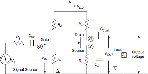
FIGURE 1 Cornon source JFET amplifier circuit
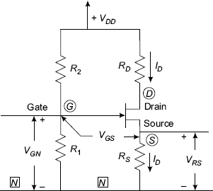
FIGURE 2 D.C. equivalent circuit of common source JFET amplifier circuit
Furthermore the effect of any shift in │ VGS │ is reduced by making │ VSN │ large compared to │ VGS. │. The same potential divider bias circuit can be used to enhancement MOSFET device amplifier circuit as shown in the Fig. 3. and also its D.C. equivalent circuit of Fig. 4 provides more clarification for the method of biasing. For DE MOSFET it needs two types of polarity voltages and this circuit is not suitable.
FIGURE 3 Common source enhancement MOSFET amplifier circuit
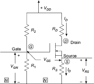
FIGURE 4 D.C. equivalent circuit of CS MOSFET amplifier circuit
Example 10 Draw the circuits of common collector amplifier and its h-parameter equivalent circuit. Derive the expressions for current gain AI, voltage gain AV, ZlN and ZOUT for the common collector amplifier circuit.
Solution Common collector transistor amplifier (emitter follower circuit).
Common collector amplifier circuit is also known as emitter Follower circuit, since the collector is at A.C. ground as can be seen from the circuit of Fig. 1. The name emitter follower arrives from the fact that the output voltage across the resistor RE in the emitter circuit is almost equal to or slightly less than input base-ground voltage (i.e. base-collector voltage) (emitter voltage follows the changes in the input signal voltage). The feedback factor β is unity as the voltage across the resistor RE is entirely feedback to the input port of the amplifier. The characteristic features of common collector amplifier are as following. The voltage gain is less than unity with no phase inversion between the input and the output signals. It has a high input impedance and low output impedance making it an ideal voltage controlled voltage source and is commonly used for impedance transformation over a wide range of frequencies. The circuit has relatively high current gain and power gain.
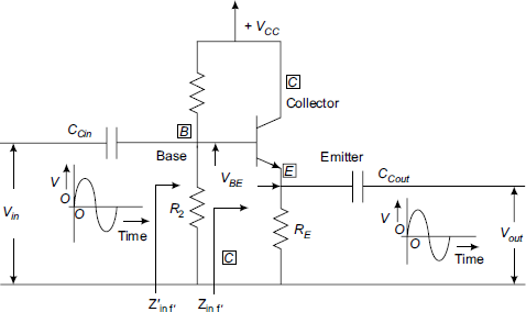
FIGURE 1 Common collector amplifier (emitter follower)
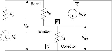
FIGURE 2 h-parameter model (A.C. equivalent circuit) for common collector amplifier (emitter follower)
h-parameter model AC equivalent circuit of common collector amplifier.
h-parameter model A.C. equivalent circuit of common collector amplifier (emitter follower) is drawn with an assumption that
hre = hoe ≅ 0 So that ![]() = ∞. That is, an open circuit and so the circuit component parallel
= ∞. That is, an open circuit and so the circuit component parallel ![]() to the output current source is omitted in the equivalent circuit of Fig. 4.42. Further, in the following analysis, the effect of R1 and R2 is not considered. The effect of R1 and R2 is to reduce the input impedance Zif to Z’if because of the effect of R1 and R2
to the output current source is omitted in the equivalent circuit of Fig. 4.42. Further, in the following analysis, the effect of R1 and R2 is not considered. The effect of R1 and R2 is to reduce the input impedance Zif to Z’if because of the effect of R1 and R2
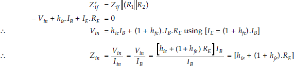
Z’if = Zif ║ (R1║R2)
–Vin + hie.IB + IE.RE = 0
∴ Vin = hieIB + (1 + hfe).IB.RE using [IE = (1 + hfe). IB]
The input impedance Zin has been enhanced by an amount [(1 + hfe). RE]
Vin = hie.IB + (1 + hfe)IB.RE
But, Vout = IE.RE = (1 + hfe).IB.RE
∴ Voltage Gain
Output impedance Z0 across the output terminals is by definition Z0 = ![]() where V is the open circuit voltage across the output terminals and I is the short circuit current. When the emitter is open, the open circuit voltage V0 is Vin = IB. hie. The short circuit current ISC = IE and ISC = IE = (1 + hfe).IB
where V is the open circuit voltage across the output terminals and I is the short circuit current. When the emitter is open, the open circuit voltage V0 is Vin = IB. hie. The short circuit current ISC = IE and ISC = IE = (1 + hfe).IB
∴ ![]()
Then, the output impedance Z0 is ![]() , a low value when compared to the input impedance Zin where, Zin = ⌊hie + (1 + hfe).RE⌋ which is relatively very large.
, a low value when compared to the input impedance Zin where, Zin = ⌊hie + (1 + hfe).RE⌋ which is relatively very large.
Example 11 Compare the features of common emitter and common collector amplifier circuits with reference to voltage gain, current gain, input resistance and output resistance.
Both voltage gain and current gains are much greater than unity for CE amplifier and so the common emitter transistor amplifier circuit is most popularly used in practice whereas, the voltage gain is approximately unity for common collector amplifier
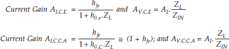
From the above two equations for current gain for both CE and CC amplifiers current gain variations with variations in load resistance are similar.
The expressions for input impedance ZIN.C.E and ZIN.C.C.A are as following
As hre ≅ 0; and if substituted in the above equation for ZIN.C.E;. the input resistance of common emitter transistor amplifier is approximately equal to hi.e of the transistor which is of the order of 1 KΩ, and varies moderately with variations in the load resistance RL; whereas the input resistance of common collector amplifier is very high and is of the order of megaohms, because hr.C ≅ 1 and when substituted in the equation for ZIN.C.C.A; the input resistance of common collector amplifier is very high and also due to voltage series negative feedback introduced into the common collector amplifier circuit.
The expressions for the output impedances of CE and CC amplifiers are as following.
From the above equation for CC amplifier, the output impedance is very low. As the common collector amplifier has very low output impedance of the order of few tens of ohms and very large input resistance of the order of megaohms, CC amplifier is used to couple between high impedance source and low impedance loads and as impedance transformation circuits and unity gain Buffer amplifier circuits.
The output impedance for common emitter transistor amplifier is the reciprocal of output admittance given as following. Further, the reverse resistance of the output junction of the CE transistor has high resistance. So, the output resistance of CE transistor amplifiers is reasonably large and is of the order of few thousands of ohms
Questions for Practice
- Discuss the need for biasing the transistor devices when used in amplifier circuits.
- Draw a transistor biasing circuit using two separate D.C. sources.
- Draw fixed biasing circuit or fixed current biasing circuit of N-P-N transistor and explain the circuit with necessary equations.
- Draw fixed biasing circuit or fixed current biasing circuit of P-N-P transistor and explain the circuit with necessary equations.
- Draw collector base biasing circuit for NPN transistor and explain the process of applying the forward bias to the input junction and reverse bias to the output junction of N-P-N transistor with necessary equations.
- Draw collector base biasing circuit for P-N-P transistor and explain the process of applying the forward bias to the input junction and reverse bias to the output junction of N-P-N transistor with necessary equations.
- Draw voltage divider biasing circuit or self-bias circuit for providing forward bias to the emitter junction and reverse bias to the collector junction of N-P-N transistor with necessary equations and explain how stability of operation of the device when used as an amplifier is achieved.
- Draw potential divider biasing circuit or self-bias circuit for providing forward bias to the emitter junction and reverse bias to the collector junction of P-N-P transistor with necessary equations and explain how stability of operation of the device when used as an amplifier is achieved.
- Obtain the D.C. load line equation for a transistor using voltage divider biasing circuit. Explain the importance of the D.C. load line in the design of voltage amplifier circuits.
- Explain the method of graphical determination of fixing the quiescent or D.C. operating point of the transistor amplifier. Discuss the specifications that are considered in the design of a transistor amplifier and any precautions that are to be considered.
- Discuss the design aspects of fixing up the circuit components of a transistor amplifier using self-biasing arrangement.
- Define the transistor h-parameters using necessary equations considering a transistor as a two-port network.
- Using a practical circuit explain the method of obtaining the input and output characteristics of a transistor.
- Draw common emitter transistor amplifier circuit with fixed bias arrangement using a single D.C. source and explain the concepts involved in the process of amplification using input and output characteristics of the device.
- Draw common emitter transistor amplifier circuit with collector to base bias arrangement using a single D.C. source and explain the concepts involved in the process of amplification using input and output characteristics of the device.
- Draw common emitter transistor amplifier circuit with self-bias arrangement using a single D.C. source and explain the concepts involved in the process of amplification using input and output characteristics of the device.
- Discuss the significance of input resistance and output resistance of an amplifier circuit, when they are used in practical circuits.
- Draw the common emitter transistor amplifier circuit. Show the wave forms at different points in the circuit with qualitative explanation.
- Draw the D.C. equivalent circuit and A.C. equivalent of CE transistor amplifier and explain their significance in the circuit analysis.
- Draw the small signal low frequency equivalent circuit of a CE transistor amplifier circuit and derive the expression for voltage gain at low frequency region.
- Draw the small signal low frequency equivalent circuit of a CE transistor amplifier circuit at mid-frequency region and derive the expression for voltage gain.
- Draw the small signal low frequency equivalent circuit of a CE transistor amplifier circuit at high frequency region and derive the expression for voltage gain.
- Draw the common base transistor amplifier circuit. Show the wave forms at different points in the circuit with qualitative explanation.
- Draw the common collector transistor amplifier circuit. Show the wave forms at different points in the circuit with qualitative explanation.
- Draw the small signal low frequency equivalent circuit of a common base transistor amplifier circuit and derive the expression for voltage gain, ZIN and ZOUT.
- Draw the circuit of an emitter follower and explain its working. Derive the expressions for voltage gain, Zin and Zout.
- Discuss the various types of biasing circuits used for FET amplifier circuit.
- Draw the common source field effect transistor amplifier circuit. Show the wave forms at different points in the circuit with qualitative explanation.
- Draw common source FET amplifier circuit with self-bias arrangement using a single D.C. source and explain the concepts involved in the process of amplification using input and output characteristics of the device.
- Discuss the purpose of various coupling capacitors and bypass capacitors used in the amplifier circuits and also mention the design criteria for component selection.
- Draw the common source FET amplifier circuit. Show the wave forms at different points in the circuit with qualitative explanation.
- Draw the common gate FET amplifier circuit. Show the wave forms at different points in the circuit with qualitative explanation. Derive the expressions for AV, ZIN and ZOUT.
- Draw the common drain FET amplifier circuit. Show the wave forms at different points in the circuit with qualitative explanation. Derive the expressions for AV, ZIN and ZOUT.
- Discuss the reasons for the absence of thermal runaway in FET devices.
- Explain the small signal A.C. equivalent circuits for FET amplifier circuits.
- Draw the mid-frequency equivalent circuit of a FET amplifier circuit and derive the expression for voltage gain mentioning the reasons for not including the effect of various capacitances in the equivalent circuit.
- Draw the typical frequency response characteristic of an amplifier and discuss the significance of the influence of coupling capacitors, shunt capacitors and the load resistors in the circuit.
- The maximum voltage gain of a transistor amplifier is 100. Low frequency cut-off frequency occurs at 1000Hz and High frequency cut-off occurs at 501KHz. Determine the bandwidth of the amplifier circuit and draw the frequency response marking the values of gain at the salient points.
- Calculate the value of gm for a transistor with ICQ = 26 mA and VT = 26 mv.
- Discuss the effect of coupling capacitors on the low frequency response of amplifiers.
- Draw the circuit of a single stage FET amplifier. Draw the mid-frequency equivalent circuit and derive the expression for voltage gain. Data: gm = 2 milli mhos; rd = 200 KΩ.; Rd = 5 KΩ. RL is very large and does not affect the load. Calculate voltage gain.
- Draw the transistor amplifier circuit using potential divider biasing arrangement with VCC = +12 volts. RC = 0.8 KΩ and RS = 0.2 KΩ. To obtain maximum output signal swings, select suitable D.C. operating point and calculate ICQ and VCEQ.
- A silicon transistor is used in a CE transistor amplifier circuit with potential divider biasing arrangement with VCC = 18 volts and RC = 1.2 KΩ. Transistor β = 100. So as to obtain symmetrical swings of output signals, the quiescent operating point is chosen with ICQ = 4.5 mA and VCEQ = 9 volts. Calculate the values of R1; R2 and RE assuming a stability factor S = 10.
- The D.C. equivalent circuit of a CE transistor amplifier with collector to base bias arrangement has VCC = 18 volts, with the component values of RC = 3.4 KΩ, RE = 0.6 KΩ. The collector to base resistance RB = 300 KΩ. Vγ = 0.7 volts and β = 100. Calculate the magnitudes of collector voltage, emitter voltage and base voltage.
- Draw the CE transistor amplifier circuit with potential divider bias arrangement having VCC = 14 volts. R1 = 21 KΩ, R2 = 7 KW; VBE = 0.5 volts; RC = 0.8 KΩ. and RE = 0.6 KΩ. Draw the D.C. equivalent circuit. Calculate the base voltage, emitter voltage, collector voltage and VCE. Comment on the results for the operation of the amplifier circuit. Design suitable values of the capacitors to be used in the circuit considering the lowest frequency of the signal to be 116 Hz.
- Draw the circuit of a common source FET amplifier with RG = 1 MΩ, RS = 0.5 KΩ and the load resistance Rd = 1.5 KΩ and VCC = 20 volts. The pinch-off voltage VP of the selected FET device is equal to – 3.6 volts. The gate to source bias voltage is to be designed at half the pinch-off voltage so as to have equal signal swings in the amplifier circuit. Calculate the magnitudes of source voltage and drain voltage. Calculate the magnitude of the input resistance, if the current through gate resistor RG is zero.
- Consider common source FET amplifier circuit with potential divider bias circuit. Draw the wave forms at salient points in the circuit and discuss the feature of 180° phase shift between the input and output signal voltages.
- Consider source follower circuit and discuss the feature of the in phase nature of output and input signals with necessary wave forms. Derive the relation for unity voltage gain.
- For an emitter follower circuit, explain with necessary wave forms how there is no phase inversion between input and output voltages. Further, discuss the relations for very high input resistance and very low output resistance of the emitter follower circuits and mention a few practical applications of the circuit.
- For source follower circuits discuss the various features in detail that made it suitable as Unity Gain Buffer Amplifier Circuits. Also, mention a few practical applications.
Points to Remember
- Electronic devices and circuits here discuss the nature of analogue signals which means that the input signals to the amplifier circuits are derived from the physical systems such as the output of a microphone of an audio system or signals from other measuring instruments such as temperature sensing devices, home appliances and so on.
- There are many types of continuous signals but the common feature of assuming an input signal is proportional to the physical quantity in nature. A sinusoidal signal is assumed in the analysis because any complex signal in nature can be represented as a combination of sinusoidal signals using network analysis and signal processing.
- Amplifier circuits are given signal voltages to be amplified at the input port, some process takes place during the signal passage through the passive circuit components and the active device whether it is a bipolar junction transistor or a field effect transistor and increased signal appears at the output port of the amplifier, which is put to the practical utility.
- As illustrated in one of the practical system of public address system, it is discussed that the processing of electrical signals is easier and using the relevant or appropriate signal conditioning transducers, the electronic circuits play a very much significant and major role in this advanced technology of various communication systems and computer technology.
- As observed in many of the present day applications such as data transfer to long distances and reception of the signals globally using cell phones, satellite communications and others, the processing of signals is one of the basic features of the communication system.
- In the amplifier circuits, the input signal, the sine wave has the representation of amplitude, frequency and the phase, which are considered for the faithful reproduction of the input signals at the receiver (or the load terminal) or any changes that may take place during transmission of signals as distortion. For understanding these concepts, it is necessary to have a strong foundation of the concepts.
- The electronic circuit is considered as an amplifier only if the output signal VOUT is greater than the input signal VIN. The amplification is defined as the ratio of the output voltage to the input voltage of the amplifier.
- The active device a bipolar junction transistor (BJT) or a field effect transistor needs biasing the P-N junctions for their working as basic amplifiers in association with D.C. supply voltage and a few passive circuit components such as resistors, capacitors and inductors.
- For a BJT to function as an amplifying device the emitter junction (input junction) of the transistor is to forward biased and the collector junction (output junction) is to be reverse biased so that the D.C. operating conditions are fixed in the active region of the output characteristics of the transistor.
- There are basically three methods of biasing the transistors using a single D.C. source and a few resistors, (a) fixed biasing method, (b) collector to base biasing method, and (c) potential divider biasing method or self-bias.
- Out of the three methods of biasing the transistor the most popular circuit is the potential divider biasing or self-biasing circuit, because of its stability of operation, as the introduction of emitter resistor has correcting features to variation in the collector current due to bias or temperature variations.
- For linear operation of the amplifiers and to provide maximum and symmetrical output signal swings, the quiescent or D.C. operating point Q is fixed at the middle of the D.C. load line drawn on the output characteristics of the transistor or FET device.
- Depending upon the practical application of the transistor amplifiers, the device specifications can be determined. Once the selection of the transistor is done, the load line is drawn below the maximum power dissipation curve on the output characteristics to determine the quiescent operating point Q.
- The coupling capacitor CC IN couples the A.C. input signal into the input port of the amplifier and at the same time blocks D.C. voltage that may be present in the signal source so that it will not effect the D.C. operating conditions of the transistor/FET.
- The input signal gets superimposed on the D.C. biasing voltages to the input junction, (emitter junction for transistor or gate to source junction of the FET device) causing varying D.C. as biasing to the devices and resulting increased values of output currents (collector current for BJT and drain current for FET) of the amplifiers.
- Output currents flowing through the load resistance develop the output voltages at the output port of the amplifiers as per design values.
- The ratio of the output voltage to the input voltage of the amplifier is known as the voltage gain of the amplifier. If voltage gains are observed for different values of input signal frequencies and plotted on a semilog or a linear graph paper the resulting characteristic of the amplifier is known as the frequency response of the amplifier.
- There will be 180° phase shift between the output and input signal voltages of common emitter transistor amplifier and common source amplifier.
- The frequency response characteristic of the amplifier is divided into three operating regions, the low frequency region, mid frequency region and high frequency region.
- The low frequency region and mid-frequency region are separated by low frequency cut-off point f1 or fL defined as the point where the voltage gain is 0.707 times the maximum voltage gain AMID in the mid frequency region or – 3db down from the mid-frequency gain when the gain is calculated as 20 log AV.
- The high frequency region and mid-frequency region are separated by high frequency cut-off point f2 or fH defined as the point where the voltage gain is 0.707 times the maximum voltage gain AMID in the mid frequency region or – 3db down from the mid-frequency gain when the gain is calculated as 20 log AV.
- If the maximum voltage gain of an amplifier is 100 in the mid-frequency region of the frequency response of the amplifier, then the gain at the low frequency and the high frequency cut-off points is 70.7.
- Once the low frequency and the high frequency cut-off points are known on the amplifier frequency response characteristic, and then the bandwidth (B.W.) of the amplifiers is the difference in high frequency cut-off point to the low frequency cut-off point. Product of gain and the bandwidth of the amplifiers is constant.
- For emitter follower circuit (common collector transistor amplifier circuit), the output voltage is taken between the emitter and the common collector of the transistor amplifier circuit. Output and input voltages are in phase. The output voltage is almost equal to the input voltage. So, the voltage gain of common collector transistor amplifier circuit is approximately unity. The emitter voltage follows the input signal voltage variations. So, the common collector transistor amplifier circuit is also known as emitter follower.
- For source follower circuit (common drain FET amplifier circuit), the output voltage is taken between the source and the common drain of the FET amplifier circuit. Output and input voltages are in phase. The output voltage is almost equal to the input voltage. So, the voltage gain of common drain FET amplifier circuit is approximately unity. The source voltage follows the input signal voltage variations. So, the common drain field effect transistor amplifier circuit is also known as source follower.
- For emitter follower circuit the input impedance is very high and the output impedance is very low. So, emitter follower circuits are used as buffer amplifiers wherever impedance transformation is required in practical electronic circuits.
- For source follower circuit the input impedance is very high and the output impedance is very low. So, emitter follower circuits are used as buffer amplifiers wherever impedance transformation is required in practical electronic circuits.
- In common base transistor amplifier circuits there is isolation between the output and input circuits. So, they are used in radio frequency amplifier circuits.
- The amplifier gain increases with increase in load resistance. When the gain of the amplifier increases its bandwidth decreases.
- The input and the output coupling capacitors in amplifier circuits affect the low frequency response of the amplifier.
- The shunt capacitances affect the high frequency response of amplifiers.
- In the mid-frequency region of amplifier response, the affects of capacitors on voltage gain is negligible and hence in the mid-frequency equivalent circuit of the amplifiers the coupling capacitors and the shunt capacitances are omitted.
- The input circuit time constant which is the product of RIN (input resistance of the amplifier stage) and the input coupling capacitance CC IN determines f1 or fL; the lower cut-off frequency or low frequency cut-off of the amplifier circuit.
- The output circuit time constant which is the product of (RC + RL) (output RC circuit of the amplifier stage) and the output coupling capacitance CC OUT affects the fL, the lower cut-off frequency or low frequency cut-off of the amplifier circuit.
- In practical circuits, no amplifier has uniform gain at all signal frequencies. In A.C. coupled amplifier circuits, where the input signal is coupled through CC IN to the input stage of an amplifier and the output signal is obtained through the output coupling capacitor CC OUT (the input and the output coupling capacitors) the associated input and the output circuit time constants affect the low frequency response of amplifier circuits. The shunt capacitances the junction capacitances of the active devices and the stray wiring capacitances affect the high frequency response of the amplifiers.
- At high frequencies, the reactance of the coupling capacitors and the bypass capacitors across the emitter or the source resistances become very small and do not have any affect on the high frequency response of the amplifier. But the device junction capacitances (the emitter junction capacitance CBE and the collector junction capacitance’CBC’) will be in parallel at the input and the output ports of the amplifier circuits. Similarly, the junction capacitances for the FET device CGS between gate and the source and CGD between the gate and the drain will be in shunt at the input and output ports of FET amplifiers that affect the high frequency response of amplifier circuits.
- The useful range of frequencies, that is, the bandwidth of the amplifiers over which the amplifier gain is reasonably uniform decides the practical application of amplifiers. Normally, the amplifier bandwidth is decided by the high frequency cut-off as the low frequency cut-off signal frequency is low compared to high frequency cut-off.
- The gain at the cut-off frequency or comer frequency or critical frequency on amplifier frequency response of an amplifier is 0.707 × AMID or –3db down the mid-band gain expressed in decibels.
- The variation of amplifier gain with input signal frequency is known as the frequency response of the amplifier and it has roll-offs (decrease in gain with frequency) at low frequency and high frequency ranges that is due to the coupling capacitors and bypass capacitors at low frequency range and due to shunt capacitances in high frequency range. The bandwidth of the amplifier is decided by the frequency response of the amplifier circuits and in turn the practical applications of electronic circuits.