Chapter 5
Feedback Amplifiers
5.1 Introduction
In this age of automation, computation and control the feedback concept plays an important role. Suppose you are driving a car, the eyes sense the position and speed of the car. Based on this input, you can modify the input by steering the wheel, apply a brake or accelerate or decelerate the engine. By the feedback, the process of driving the car is controlled.
Suppose you want to control an electric motor that rotates an antenna, the process is called rotating an antenna. And, the controlled variable is the angle of position of the antenna, which is to be sensed, and based on the feedback of angular position; steering the antenna to the desired position can control the motor. Similarly, in the case of an amplifier sampling a part of the output voltage or current feedback to a network can control the process of amplification. Whereby an error is generated between the input signal and output signal, which is feedback to an amplifier to obtain the desired response. Presently microprocessor based control systems are available.
In all these cases the output is sensed and fed back to the input and depending on the error between input and feedback controlling action takes place. This is similar to Closed Loop Control System.
5.2 Negative Feedback Amplifiers
Negative feedback amplifier is one wherein the feedback voltage or current is in phase opposition to the input source voltage or current.
The single loop negative feedback amplifier system shown in the Fig. 5.1 consist of the following components.
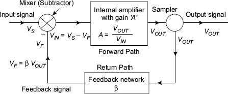
FIGURE 5.1 Block diagram of an ideal single loop negative feedback amplifier
- An ideal or internal amplifier whose gain is A. VIN is the input signal and VOUT is the output signal of the internal amplifier. The ratio of the output voltage to the input voltage is called as forward gain or open loop gain A (voltage gain without any feedback arrangement).
- Voltage or current is sampled by means of suitable sampling network samplers and fed to feedback network.
- A part of the output VOUT so derived from the feedback network VF is applied into the amplifier through a mixer wherein the input signal VS and feedback signal VF are combined, so that VIN = VS – VF, which is the difference or error signal. Thus, the feedback signal reduces the effective input signal.
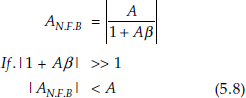
This type of arrangement is known as negative feedback or degenerative feedback in amplifier circuits. The resulting amplifier circuit is called as negative feedback amplifier. The overall gain of the negative feedback amplifier AN.F.B is referred as closed loop gain, that is, the gain from the input to the output with the presence of feedback arrangement. The gain of the negative feedback amplifier decreases because of reduction in the effective input signal VIN.
Voltage Gain ANF
Output voltage of internal amplifier V OUT = A.VIN (5.1)
Feedback voltage VF = β.V OUT (5.2)
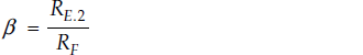
β is known as reverse transmission factor or feedback factor. It may be a real number or a complex function of frequency of signals.
But VIN = [VS − VF] (5.3)
∴ VOUT = A.VIN = A.[VS − VF]
VOUT = A.[VS − β.VOUT] UsingVF = β.VOUT (5.4)
Rearranging the terms VOUT [1 + Aβ] = A.VS
∴ Gain of the negative feedback amplifier = ![]()
In the above discussion, the feedback signal VF is in phase opposition to VS. This type of feedback is called negative feedback. It is widely used in amplifier design for stable operation. The negative feedback is also known as degenerative feedback or inverse feedback. Aβ is known as loop gain or return ratio or loop transmission factor. Loop gain is the product of the internal amplifier gain A (forward gain) and the feedback factor β and totally refers to the gain right around the loop.
The voltage gain of the negative feedback amplifier AN.F decreases, which is clear from the equation (5.5). Even if there is a reduction in feedback amplifier gain, the negative feedback system improves the performance of the system. Especially the variations in gain and other parameters of amplifiers such as distortion are reduced for better linearity and stability in the working of closed loop system or negative feedback amplifiers as the case may be.
The magnitude of feedback introduced into the amplifier is expressed in decibels (db).
Taking logarithms on both sides of the equation (5.5)
AN.F in (db) = A in (db) – [1 + Aβ] in (db) (db is decibels)
AN.F in (db) = A in (db) + N (db), for negative feedback amplifier, N is negative.
Concept of Positive Feedback In case of the positive feedback signal VF is in phase with VS, then VI.N = [VS + VF] and the type of feedback is said to be positive feedback.
In this case, the gain with positive feedback increases. If loop gain Aβ = 1 the gain becomes ∞ (infinity). Then, the circuit cannot be used as a normal amplifier. The concept of positive feedback is used in the design of oscillator circuits.
Essential Constituents of Negative Feedback Amplifier
- Basic or internal amplifier: The amplifier has voltage gain A. The device features may be modified depending upon the application and stability of operation is achieved.
- A sampling network (voltage sampler or current sampler): Depending upon the type of negative feedback amplifier, the magnitude of output parameter, voltage or current sampling is used.
- Feedback networks are usually two-port networks containing passive circuit components such as resistors or capacitors or inductors (RE in the emitter path of transistor amplifiers and RS in the source path of FET amplifiers explain this). Negative feedback arrangement is employed in the feedback network. The sampled parameter is connected from the output port to the input port as feedback signal as shown in the circuit of negative feedback amplifier of Fig. 5.1, through the feedback network.
- A mixing or subtracting network or circuit elements where input signal and the feedback signal are mixed or processed to get difference or error signal to be applied to the internal or the basic amplifier.
5.3 General Characteristics of Negative Feedback Amplifier
In a closed loop amplifier the feedback voltage or current is sampled and the feedback signal is applied in anti-phase with the input signal through a mixer and the error signal is fed to the amplifier as shown in Fig. 5.1.
The voltage gain of the negative feedback amplifier AN.F is reduced below that of open loop gain A of internal amplifier, which is clear from the equation (5.6). This is due to the fact that the feedback signal causes a reduction or cancels a portion of the input signal and the effective input signal in operation is smaller than the signal without negative feedback, resulting in a consequent reduction of gain of the overall negative feedback amplifier stage.
It is already derived that the gain of negative feedback amplifier is given by
Therefore, the voltage gain of negative feedback amplifier decreases. But it is extensively used in amplifiers because of various merits like reduction in wave form distortion, increase in amplifier bandwidth (improved frequency response characteristics), because the product of gain and bandwidth of amplifier circuits is constant; stability of amplifier operation against the variations in device parameters and parameter changes due to temperature variations and modification of input and output impedances for various practical applications. Thus, the performance of transistor amplifiers is enhanced.
The improvement in performance of the negative feedback amplifiers (transistor amplifiers) is due to the following features.
1. Reduction of Frequency and Phase Distortion Wave form distortion due to the non-linearity of the active device characteristics.
Voltage gain of negative feedback amplifier AN.F.B = ![]()
If the amplifier gain is very large so that Aβ >> 1
Now, the gain ANFB of the feedback amplifier is independent of the gain A of the internal amplifier in the forward path. The equation (5.9) means that the negative feedback in amplifiers has brought the amplifier out of the many inherent disadvantages as discussed below. The sacrifice in gain has brought many of the following advantages for a better performance of the negative feedback amplifier.
Under these conditions the overall gain of negative feedback amplifier is purely dependent upon β of the feedback network. And as such, any changes in the active device parameters, ageing and temperature changes, and supply voltage fluctuations do not have any effect on the gain of negative feedback amplifiers also. If the feedback network contains only resistive elements the gain becomes independent of frequency. So, there is substantial reduction in the frequency and phase shift distortion. Passive components, the capacitors and resistors with high precision can also be used in the feedback path to stabilise the response of negative feedback amplifiers. Thus, the stabilisation of amplifier gain is achieved. This is the most desirable characteristic of amplifier systems and in turn the practical electronic systems, because of the presence of amplifier circuits in most of the applications.
2. Stability of Gain of Negative Feedback Amplifier
Differentiating the above expression for gain of negative feedback amplifier with respect to A.


The fractional charge in amplification with feedback is related to fraction charge without feedback by the relation
S is defined as the sensitivity factor or transfer gain T
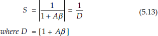
D = [1 + Aβ] is called desensitivity or return difference (5.14)
S is also known as sacrifice factor and it is a ratio of ![]() (5.15)
(5.15)
Fractional change in gain A is reduced by the desensitivity factor D. Changes in output voltages or currents are feedback inputs and as such error changes in opposite direction effecting the output to be independent of changes in the basic amplifier gain. Thus, the overall stability is improved against parameter changes in a negative feedback amplifier.
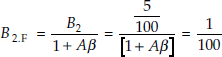
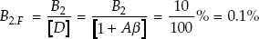
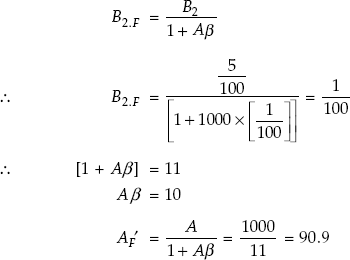
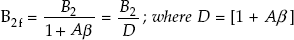
3. Reduction in Non-Linear Distortion Wave form distortion is produced when the amplifier gain is not uniform for large input signal swings extending into nonlinear region of the device characteristics. Assume the presence of second harmonic terms (dominant component of harmonic distortion due to non-linear amplitude response in power amplifiers) when a sinusoidal input signal is applied to large signal amplifiers as in power amplifiers. Second harmonic distortion B2 is assumed in the output of internal amplifier in the absence of feedback for analysis.
If negative feedback is applied, second harmonic signal B2F is generated in the output of the active device. The feedback network receives sampled output and applies a feedback voltage of magnitude –βB2.F at the input port of the internal amplifier. This results in – Aβ.B2.F in the output. Now, the output voltage VOUT contains two components (1) The original distortion component B2 when no feedback is introduced in the circuit and (2) A. β. B2F due to the introduction of negative feedback into the amplifier forming a closed loop. Thus, there is reduction of second harmonic distortion by a factor D in the negative feedback amplifier as analysed below.

Thus, the second harmonic distortion content B2 in the output signal of a normal power amplifier becomes B2F due to the introduction of negative feedback into the amplifier by getting reduced by a factor [1 + Aβ] as shown in the equation (5.17).
4. Reduction of Noise If there is a noise source inside a system, application of negative feedback reduces noise by a factor D = [1 + Aβ]. So, the performance of the amplifier is improved. In this connection it is to be mentioned that signal to noise ratio will not have any effect. Further, if the noise is extraneous to amplifier design modification is to be made to reduce noise.
The hum introduced by a poorly designed direct current supply decreases considerably by using negative feedback.
5. Input Impedance Z IN.F The effect of negative feedback on ZIN, the input impedance of the amplifier depends upon feedback connection types of an amplifier. Shunt feedback decreases input impedance by a factor D = [1 + Aβ] and for series feedback amplifier the input impedance increases by a factor D.
6. Output Impedance Zoutf The effect of negative feedback on ZOUT, the output impedance of the amplifier depends upon feedback connection types of an amplifier. The output impedance decreases by a factor D with voltage shunt feedback and with current feedback the output impedance increases by a factor D.
7. Improvement in Frequency Response In negative feedback amplifier, the 3 db bandwidth stretches or increases (improves).

where |
Am = midfrequency gain with out feedback |
|
AH.F = high frequency gain without feedback |
The overall gain of negative feedback amplifier AN.H.F. becomes as following.

Dividing both numerator and denominator of (5.18) by (1 + βAm)

From the above expression (5.19) f2.F.B = f2 [1 + Am.β], the bandwidth of negative feedback amplifier is increased by the factor [1 + Am.β] (The gain bandwidth product of an amplifier is constant. As the gain of negative feedback amplifier decreases, the bandwidth increases).
Midfrequency amplification with feedback Am.F is equal to the midband amplification with out feedback Am divided by [1 + βAm].
The upper 3db frequency with feedback f2.F.B equals to the corresponding 3db frequency without feedback f2 multiplied by the same factor [1 + βAm].
Gain bandwidth product with feedback.
Thus, the gain bandwidth products with feedback and without feedback for amplifier circuits are the same. Similarly, it can be shown that lower –3db frequency with feedback f1.F.B is decreased by the same factor [1 + β.Am]
Using negative feedback in amplifier circuits, the lower half power frequency is decreased and higher half power frequency is increased, which is shown in the frequency response of amplifier circuits for both the situations in the Fig. 5.2. The low frequency cut-off f1 is very much less than the high frequency cut-off f2 for amplifiers. Hence, the bandwidth of the amplifiers is usually decided by the high frequency response of the amplifier circuits.

FIGURE 5.2 Frequency response of amplifiers with and without negative feedback
With negative feedback, the amplifier gain is reduced and hence the amplifier bandwidth (B.W) is increased.
Summarising the above advantages of negative feedback amplifier, we find that
- There is reduction in frequency and phase-shift distortion.
- Stability of the gain is improved.
- Non-linear distortion is reduced.
- Noise is reduced.
- Input and output impedances of various amplifiers can be altered.
- Bandwidth stretching occurs due to increase in the 3 db bandwidth of the amplifier.
- The gain bandwidth product is unaltered.
Disadvantages The gain gets reduced with negative feedback. As the advantages overweigh the disadvantages, negative feedback is extensively used in negative feedback amplifiers, complex control systems, robotics, mechatronics, econometrics and modelling.
5.4 Classification of Negative Feedback Amplifiers
There are four types of feedback amplifiers:
- Voltage series feedback amplifier
- Voltage shunt feedback amplifier
- Current series feedback amplifier
- Current shunt feedback amplifier.
5.5 Voltage Series Feedback Amplifier
In voltage series feedback amplifiers, output voltage VOUT is sampled and connected in series with the external input signal Vs at the input port of the amplifier as feedback voltage VF through a two-port feedback network (so as to cause negative feedback). Thus, a part of the output voltage is feedback as VF to the input port of the amplifier, resulting in an overall gain reduction due to negative feedback. When there is no feedback process, feedback voltage VF = 0. Then, the voltage gain AV of the simple amplifier stage is the ratio of the output voltage VOUT to the input voltage VIN
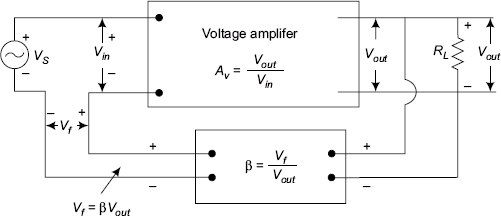
FIGURE 5.3 Voltage amplifier with voltage series feedback
If a feedback signal Vf in this case is connected in series opposition with the input signal so that
VIN = (VS − VF)
VOUT = AV.VIN = AV[VS − VF]
∴ VOUT = AV.[VS − β.VOUT]

FIGURE 5.4 Voltage series feedback amplifier-equivalent circuit
where AF.(V.S.F.B) is the voltage gain of the voltage series feedback amplifier.
Due to negative feedback in the voltage amplifier, the gain is reduced by a factor (1 + Av.β).
Voltage series feedback amplifier (using Thevinin’s equivalent circuits) to calculate input impedance ZIN.F and output impedance ZOUT.F is shown in Fig. 5.4.
Input Impedance From the diagram of figure 5.4.
∴ IIN.ZIN = VS − AβVIN
IIN.ZIN = VS − A.β.ZIN.IIN
Rearranging the terms ZIN.IIN[1 + Aβ] = VS (5.26)
Input impedance of V.S.F.B.A = ZIN.F = = ZIN (1 + Aβ) (5.28)
The input impedance of the voltage series feedback amplifier ZIN.F increases by a factor (1 + Aβ).
Output Impedance ZOUT.F is the output impedance, which is the impedance looking at the output port for the amplifier with RL disconnected. To find the output impedance, load resistance RL is disconnected and VS is made zero.
∴ IS = 0
Applying a voltage V across the output terminals, the resulting current I is calculated. Output impedance of feedback amplifier
From the equivalent circuit diagram
When VS = 0; VIN = [VS − VF] = −VF = −β.VOUT = −β.V (5.31)
Therefore, equation (5.30) becomes
∴ V [1 + AVβ] = I.ZOUT (5.32)
By definition, the output impedance of the voltage series feedback amplifier is reduced by a factor (1 + Avβ), where (1 + Avβ) is called as desensitivity factor D.
The output terminal impedance Z| OUT.F of the amplifier including ZL is where Z’O = Z0 || ZL is the output terminal impedance without feedback but with ZL connected in the circuit
Emitter Follower A practical voltage series feedback amplifier circuit is emitter follower in the case of transistor amplifier circuits.

FIGURE 5.5 Voltage series feedback amplifier (emitter follower)
The output voltage developed across RE is fully applied back to input port so that this feedback voltage VF is in series opposition with the input voltage VS (the emitter voltage follows the variations in the input signal voltage and hence known as emitter follower). The feedback factor
VOUT = IE.RE = [1 + hfe].IB.RE (5.35)
But VS = hie.IB + IE.RE = hie.IB + (1 + hfe) IB.RE
∴ VS = [hie + (1 + hfe).RE].IB

This amplifier circuit of Fig. 5.5 provides the operation with voltage series feedback arrangement according to the previous analysis for ZIN.F and ZOUT.F the emitter follower circuit has a very high input impedance and very low output impedance. This circuit is used in the front end of various electronic test instruments and also as a unity gain buffer amplifier, while cascading amplifiers as in multistage amplifier, voltage series feedback is preferred in front end.
FET Source Follower Circuit Common drain amplifier to illustrate voltage series feedback amplifier operation.

FIGURE 5.6 Voltage series feedback amplifier (source follower)
The output voltage VOUT across RL or RS is the sampled signal voltage that is fedback to the input so that VF is in series opposition with the input signal voltage VS so that VIN = (VS – VF).
This type of operation causes negative feedback arrangement with voltage series feedback mechanism.
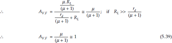
Voltage gain of FET amplifier
where, RL = load resistance and rd is the drain resistance of FET device.
Or,
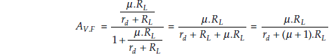
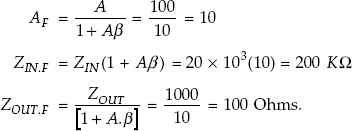
Example FET source follower has RL = 2.5 KΩ. The device parameter of the FET are gm = 400 × 10–6 mhos, µ = 20 and rd = 50 KΩ. Calculate AV; AF.N.F.B; ZOUT.F; ZIN.F and feedback factor β. For the FET source follower circuit, when considered as voltage series feedback amplifier,
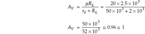
Desensitivity factor |
D = [1 + AV.β] |
|
D = [1 + 0.96 × 1] |
|
D = 1.96 |
(β = 1 for source follower) |
|
Gain of feedback amplifier |
|
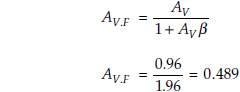
The input resistance of FET device ZIN.F is very high.
ZIN.F = ZIN (1 + Aβ) is also very high.
Output impedance of FET amplifier will be
The output impedance decreased to a low value.
Source follower circuits function for impedance transformation and buffer amplifiers.
In general, negative feedback amplifiers are categorised into the following four groups:
- Voltage series feedback amplifier
- Voltage shunt feedback amplifier
- Current series feedback amplifier
- Current shunt feedback amplifiers.
The classification can also be made into two groups with two modes of operation in each group based on the principles of working of the amplifiers.
I) Sampling
(a) Voltage Voltage can be sampled only by connecting a variable resistance, a potentiometer across the output terminals, (output port of the amplifier).
(b) Current Current can be sampled by breaking the circuit at the output port and adding the feedback network in series. By adding the feedback network automatically couples the output into the input port.
II) Type of Connection at the Input Port
- If the feedback quantity is to be connected in series, the quantity should always be voltage, that is, it is Vf irrespective of whether the parameter sampled is voltage or current.
- On the other hand, if it is to be connected into the input port in shunt, then it should always be current, that is, If irrespective of voltage or current sampling being done.
We can neither connect in series a current sample to a current source, nor can connect a voltage sample across a voltage source.
So, invariably series feedback requires Vf and shunt feedback requires If.
Therefore, the above two types of categories form the types of classification depending upon the working principles of the amplifiers for the corresponding four types of basic amplifiers.
Voltage Series Feedback Amplifier Circuit
In the voltage series feedback amplifier circuit of Fig. 5.7, forward bias to the emitter junction and reverse bias to the collector junction of the transistor are provided by the supply voltage VCC and R1 and R2 so that the transistor T acts as a basic amplifier. Emitter resistor RE stabilises the bias. The decoupling capacitor CE keeps the emitter of the transistor at A.C. ground. The output voltage VOUT is sampled by using a potential divider using the two resistors R3 and R4. The voltage across the resistor R4 provides the feedback voltage VF.

FIGURE 5.7 Voltage series feedback amplifier (practical circuit)
If R3 = 9 KΩ and R4 = 1 KΩ then ![]()
If the voltage gain of the amplifier AV without feedback is much greater than one, the gain of the negative feedback amplifier AN.F.B is equal to [β]–1. Then, the gain of the negative feedback amplifier AN.F.B = 10, using the value of β = 0.1 as calculated previously.
From the circuit, it is clear that VF is connected in series opposition to VS the signal voltage and thus contributing voltage series negative feedback in the amplifier circuit. The one disadvantage with the circuit is that the signal source cannot be grounded and should be isolated from the ground.
As seen in the previous derivations the input impedance increases, the output impedance decreases, voltage gain decreases but provides stable operation against device parameter variations, reduction of distortion and increase of bandwidth and so on.
Example 1 In voltage series feedback amplifier of Fig. 5.7; RC = 2 KΩ. gm = 50 millimhos. The feedback factor β = 0.1. Calculate the gain of the amplifier with and without feedback.
Solution Assume hOE = hre = 0
Gain of amplifier without feedback AV = – gm.RC = – 50 × 10–3 × 2 × 103 = 100
As Aβ = 100 × 0.1 = 10 > 1, the gain of the amplifier with feedback Av.F is as following
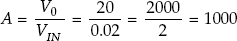
Example 2 Calculate the gain, input impedance and output impedance of voltage series feedback amplifier having gain A = –300; RIN = 1.5 KΩ and ROUT = 50 KΩ; β = 0.05.
Calculate voltage gain, input impedance and output impedance of the amplifier circuit.
Solution Calculation of gain
Calculation of Input impedance
ZIN.F = ZIN [1 + A.β] = RIN [1 + A.β] = 1.5 × 10³[1 + 300 × 0.05] = 1.5 × 103 × 16 = 24 KΩ
Calculation of output impedance
5.6 Voltage Shunt Feedback (Shunt-Shunt) Amplifier
The output voltage is sampled and feedback output from the feedback network is connected in shunt across input signal and input port of the amplifier. Voltage shunt feedback is also called as shunt-shunt feedback from the way the process goes on in the amplifier circuit.
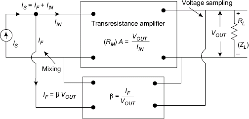
FIGURE 5.8 Block diagram of voltage shunt feedback amplifier
In voltage shunt feedback amplifier or transresistance amplifier, sampling parameter at the output port is the voltage VOUT. Since the feedback connection at the input port of the amplifier is shunt type, the feedback parameter is current IF.
Voltage gain of feedback amplifier AV.F =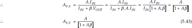
The gain factor ![]()
Gain factor with feedback ![]()
but IS = IIN + IF

The Voltage shunt feedback amplifier is represented as equivalent circuit in the Fig. 5.9.

FIGURE 5.9 Equivalent circuit representing current controlled voltage source
The input impedance ZIN.F is calculated from voltage shunt feedback amplifier of Fig. 5.8.
Input impedance ![]()
Input impedance with feedback ![]()
But IS = IIN + IF

Therefore, the input impendence with feedback ZIN.F decreases by a factor [1 + βRm] or [1+Aβ] in voltage shunt negative feedback amplifier circuits.
The derivation for output impendence ZOUT.F is same as shown for the voltage series feedback amplifier
This type of feedback amplifier is called transresistance amplifier or I to V (current to voltage) converter as shown in the following Fig. 5.10.

FIGURE 5.10 Equivalent circuit representing voltage shunt feedback amplifier
Voltage Shunt Feedback Amplifier Circuit
Voltage shunt feedback amplifier in the Fig. 5.11 is a common emitter amplifier with input signal VS and the output voltage VOUT. The resistor RF is connected between the collector terminal and the base terminal of the transistor; sampling the output voltage and linking to the input port for feedback signal mixing with the input current. The feedback current IF through the shunt resistor connecting the output and the input ports of the feedback amplifier is as following.
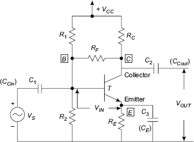
FIGURE 5.11 Voltage shunt feedback amplifier (practical citcuit)
∵ open loop gain A is very large
∵ IF = β.VOUT considering, ![]()
If loop gain Aβ >> 1
overall gain of the feedback amplifier ![]()
The transresistance RM = Af = ![]()
5.7 Current Series Feedback Amplifier Circuit (Series-Series Type Amplifier)
Fig. 5.12 represents a current series feedback (series-series) amplifier circuit, which is also known as (transconductance amplifier).
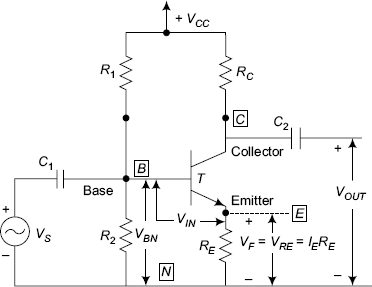
FIGURE 5.12 Current series feedback amplifier (practical circuit)
The circuit in Fig. 5.12 behaves as current series feedback amplifier as following. The circuit is a common emitter transistor amplifier with the difference that the emitter resistor RE is not decoupled with A.C. signals by using the bypass capacitor CE. This means that the emitter is not grounded even for A.C. signals. Since the resistor RE is common for both the input and the output circuits, it contributes or provides feedback. Since the output current flows through RE the sampling of the parameter is the current sampling at the output port. This current IE flowing through the emitter resistor RE develops a voltage IE.RE with the emitter terminal positive compared to the ground terminal N as shown in the Fig. 5.12.
The voltage across RE, that is, IE.RE known as VRE is the feedback voltage, Vf; that opposes the voltage, VBN across R2 and feedback to the input port of the amplifier. The actual signal input VBE or VIN to the amplifier will be VBN – IE.RE; or (VS – IE.RE) that is, the input signal voltage VS minus the feedback voltage Vf. Thus, the sampling is series sampling of the current at the output port and coupling is series type of feedback voltage at the input port of the amplifier for introducing negative feedback into the circuit. Hence, the circuit is a current series feedback amplifier. The circuit is also known as series sampled-series feedback amplifier.
Feedback factor
The gain factor is
Gain of feedback amplifier Af = −gm.RL = −gm.RC (5.55)
This can also be verified from gain expression using h-parameters
Also, it can be derived that ZIN.F = ZIN(1 + gm.β) = ZIN(1 + gm.RE) (5.58)
and,ZOUT.F= ZOUT (1 + gm.β) = ZIN(1 + gm.RE) (5.58)
The following block diagram shown in the Fig. 5.13 explains the following features in the circuit. 1) The concept of forward path amplifier known as transconductance amplifier by context of the input and the output signals to the amplifier. 2) The method of sampling the current at the output port. 3) The method of feeding the signal voltage VF in series with VS to cause mixing of the signals to provide negative feedback. Thus, the figure explains the basic principles of current series feedback amplifier, which is also known as transconductance amplifier.

FIGURE 5.13 Transconductance amplifier (current series feedback amplifier)
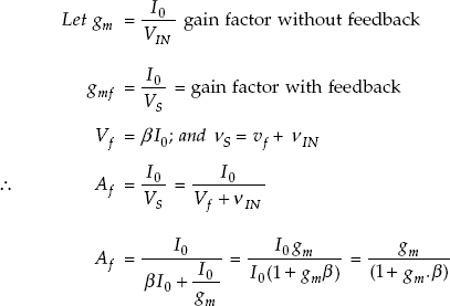
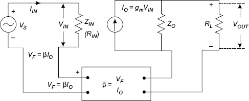
FIGURE 5.14 Equivalent circuit representing a voltage controlled current source current series feedback amplifier-equivalent circuit
Input impedance without feedback ![]()
Input impedance with feedback ![]()
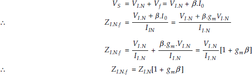
Current-Shunt Feedback (Series-Shunt) Amplifier
The output current is sampled in this feedback amplifier and applied in shunt to input of the amplifier. It is also called series derived shunt-fed feedback.
FIGURE 5.15 Block diagram of current shunt feedback amplifier
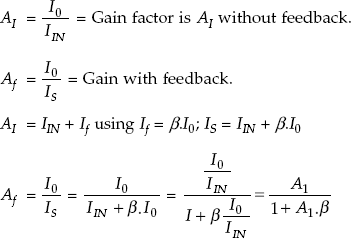
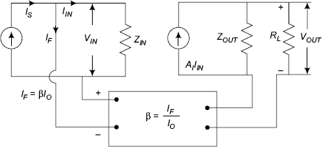
FIGURE 5.16 Equivalent circuit to determine input impedance with feedback current shunt feedback amplifier-equivalent circuit
Input Impedance with Feedback ZI.N.f
where,
Therefore, the input impedance of current shunt feedback amplifier; ZI.N.f is reduced by the factor [1 + AI.β].
The output impedance ZOUT.F is given in the following expression
Output impedance with current shunt feedback has increased by a factor [1 + AI.β].
5.8 Current Shunt Feedback Amplifier
Current shunt feedback amplifier shown in the Fig. 5.17 is a two-stage amplifier with the emitter resistance RE2 of the second stage amplifier unbypassed and a resistor RF is connected between the emitter E2 of transistor T2 and the base B1 of the transistor T1 to provide current sampling and shunt feedback arrangement as explained below.
Between the output voltage VOUT–1 of transistor T1 and the input voltage VIN–1 of transistor T1; there is phase shift of 180° (CE amplifier). Between the input voltage VIN–2 of transistor T2 and the output voltage VOUT–2 at the emitter terminal of the transistor T2 there is no phase shift (emitter follower). Hence, if a part of IC.2 (IC.2 ≅ IE.2) from the emitter of T2 is fed back at the base of T1 through RF; it means current sampling and shunt connection with phase shift of 180° between the feedback signal and the input signal to the first stage. Thus satisfying the condition for negative or degenerative feedback.

FIGURE 5.17 Current shunt feedback amplifier
In the analysis of the current shunt feedback amplifier circuit, the resistance RF is replaced by applying the Miller’s theorem by calculating the voltage gain between the base of T1 and the emitter of T2 and if this is considered as AV.B1.E.2; then RF is replaced by
Between base B1 and ground and RF.2 = RF across RE.2 and then analysis can be done treating it as a network using equivalent circuit for transistors T1 and T2.
The resistor RF is across the two points B1 and E2 in the amplifier circuit shown in the Fig. 5.17. So, the feedback current If is according to the following equation,
But VOUT–2 = −IOUT.RE.2
∴ Feedback factor
Current gain with feedback = AI.f
It is already known that Af = β−1 = ![]() when Aβ >> 1.
when Aβ >> 1.
Therefore, the current gain of the feedback amplifier, AI.f, where
The output resistance ROUT.F with feedback is the parallel combination of the emitter resistor RE.2 of the second transistor and the equivalent Miller resistance of feedback resistor at the output port RF.2 = RF
On similar lines the input resistance with feedback RIN.F is the parallel combination of the effective Miller resistance RF.1 of the feedback resistor RF at the input port of the first stage of the amplifier and the input resistance hi.e of the first transistor T1.
The expression for RF.1 is repeated here for convenience.

Summary of feedback amplifiers

Note:
- For series comparison Zif > Zi.n
- For shunt mixing Zif < Zi.n
Solved Examples
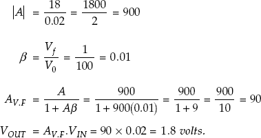
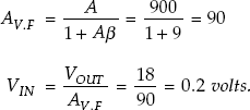
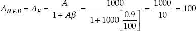
Example 1 An amplifier without feedback produces a fundamental component of output voltage of 30 volts with second harmonic component B2 in the output of amplifiers due to non-linearity of 5% distortion content when input voltage VIN is 0.02 volts.
- Calculate the open loop gain of the amplifier.
- If 1% of the output is fed back to the input as a negative voltage series feedback, calculate the magnitude of the output voltage.
- If the fundamental frequency component of the output voltage is maintained at 30 volts, but the second harmonic distortion B2.F is reduced to 1%, calculate the input voltage.
Solution Open loop gain A
Gain with feedback
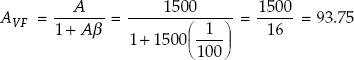
Output voltage with feedback
As the output voltage is maintained at 30 volts there will be no change in distortion.
∴ 1 + Aβ = 5
Required magnitude of input voltageVIN =
Example 2 The basic amplifier has a gain of – 1000 and β = – 0.10. If due to temperature change, the amplifier gain changes by 10%, calculate the % change in the gain of amplifier with feedback.
Solution

Therefore, the negative feedback introduced into the amplifier reduces the amount of changes in gain due to temperature changes considerably. This is one of the major advantages of negative feedback amplifiers while there is reduction in gain of the amplifier (a disadvantage).
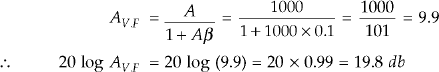
Example 3 An amplifier has an open loop gain of 1000 with an input signal voltage VIN of 10 mv and second harmonic distortion B2 is 10%. If 40 db negative voltage series feedback is applied to develop same output signal voltage with the same distortion content, determine 1) gain with feedback, 2) second harmonic distortion, 3) required input voltage.
Solution Magnitude of feedback = 40 db; VIN =10 mv
Open loop gain = A = 1000; Feedback factor β = 0.1
- Gain with feedback = AV.F

Voltage gain of the negative feedback amplifier

- Second harmonic distortion content B2.F of negative feedback amplifier is as following
Second harmonic distortion is reduced to a low magnitude with negative feedback in amplifiers.
- Required magnitude of the input signal voltage VS,

Example 4 Consider an amplifier with an open loop gain of 2500 ± 100. Negative feedback is introduced into the amplifier so that the voltage gain will not undergo a change more than ± 0.1% Calculate: 1) Feedback factor β (inverse transmission ratio) and 2) Voltage gain with feedback AV.F to achieve the above result.
Solution
∴ A.β = 39
Hence, feedback factor ![]()
Reverse transmission ratio (feedback factor) β = 0.0156.
Gain with feedback = AV.F
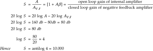
Example 5: A negative feedback amplifier has open loop gain AV of 160 db and with negative feedback the gain is AV.F = 80db. Calculate the sacrifice factor S.
Solution:
Example 6 An amplifier without feedback produces an output voltage VOUT at the fundamental frequency of the signal of 18 volts with 100% second harmonic distortion, when the input is 0.02 volt.
If 1% of the output is feedback to the input in negative voltage series feedback, calculate 1) output voltage, if the fundamental frequency component is maintained at 18 volts, and second harmonic distortion content is reduced to 10%, 2) required input voltage.
Solution
- Calculation of the output voltage VOUT
- Calculation of the required input voltage, VIN

If the output is maintained at 18 volts, the required magnitude of input voltage VIN is calculated as following:
Example 7 A negative feedback amplifier has a voltage gain of 60 db and uses 0.1 of the output voltage in the feedback, calculate the gain with feedback in db.
Solution
Open loop gain A = 60 db
20 log A = 60db
∴ log A = ![]() = 3
= 3
∴ Gain A = antilog ![]() = antilog 3 = 1000
= antilog 3 = 1000
Gain with negative feedback AV.F
Feedback factor
Example 8 Voltage gain of an amplifier is 60 db. It is decreased to 20 db when negative feedback is introduced into the amplifier. Calculate the feedback factor and the open loop gain A.
Open loop gain A = 60 db
∴ 20 log A = 60 db
Open loop gain A = antilog10![]() = antilog 3 = 1000
= antilog 3 = 1000
Gain with negative feedback AV.F = 20 db
20 log AV.F = 20 db
∴ AV.F = antilog ![]() = antilog 1 = 10
= antilog 1 = 10
∴ AV.F = 10
Feedback factor ![]()
Example 9 A negative feedback amplifier has midband gain Am of 1000. The 3-db frequencies f1 and f2 before the introduction of negative feedback into the amplifier are 500 Hz and 5.5 MHz, respectively. The feedback factor β = 9 × 10⁻³
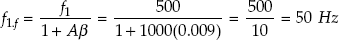
Calculate the following parameters:
- Gain with feedback AV.F
- Lower half power frequency after feedback
- Upper half power frequency after feedback
- Gain bandwidth product after feedback
- Gain bandwidth product before feedback.
- Gain with feedback AVm.F
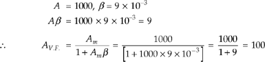
- Lower half power frequency after feedback f1.f
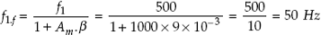
- Upper half power frequency after feedback f2.F
f2.F = f2(1 + Am.β) = 5.5 × 10⁶[1 + 1000 × 9 × 10−3] = 5.5 × 106 × 10 = 55 × 106 = 55 MHz.
- Bandwidth (B.W) of a negative feedback amplifier ≈ 55 MHz
Gain × Bandwidth of negative feedback amplifier = AV.F × B.W = 100 × 55 MHz = 5500 MHz
- Bandwidth of amplifier without feedback = 5.5 MHz
Gain × B.W. of amplifier without feedback = 1000 × 5.5 MHz = 5500 MHz.
Thus, it is clear that the product of gain and bandwidth of amplifiers remains the same.
- Gain with feedback AVm.F
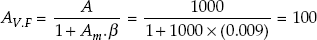
Example 10 An RC coupled amplifier has midband frequency voltage gain Am of 1000. The half-power frequencies are f1 = 500 Hz; f2 = 550 KHz and distortion content D of 10% in the amplifier without feedback. Find the amplifier voltage gain AV.F, f1f and f2f and distortion Df when negative feedback is introduced into the amplifier with a feedback factor β of 0.009.
Solution Data: Open loop gain A = 1000
Feedback factor β = 0.009
Lower cut-off frequency f1 = 500 Hz
Upper cut-off frequency f2 = 550 KHz.
Distortion D = 10%
- Voltage gain with feedback AV.F
- Lower half power frequency with feedback f1.f
- Upper half power frequency with feedback f2.f
f2.f = f2[1 + A.β] = 550 × 103[1 + 1000 × 0.009] = 550 × 103 × 10 = 5500 × 103 = 5.5 MHz.
- Distortion present in feedback amplifier Df
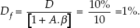
Thus, the distortion is very much reduced with negative feedback in amplifiers.
The bandwidth of negative feedback amplifier has increased considerably at the sacrifice of gain AV.f for negative feedback amplifier, satisfying the basic fact that the product of gain and bandwidth of amplifier is constant. At the same time the distortion content is also reduced with negative feedback introduced into the amplifier circuits.
Example 11 The open loop gain or forward path gain A of an amplifier is 50,000. When negative feedback is introduced into the amplifier, the gain is decreased to 10,000. Calculate the feedback factor and express the gain with negative feedback in db.
Solution
Open loop amplifier gain A = 50,000
Gain of the negative feedback amplifier AN.F.B = AF = 10,000

Amount of negative feedback
Feedback in
Example 12 In a voltage series negative feedback amplifier, the internal amplifier has a gain A = –100, input resistance ZIN = 20 KΩ, output resistance Zo = 103 Ω. When feedback of β = – 0.09 is introduced into the amplifier, determine voltage gain, AF, output impedance, ZOUT.F and input impedance, ZIN.F.
Solution If open loop gain A = –100, feedback factor β = –0.09
Voltage gain with feedback
Example 13 An amplifier without feedback gives an amount of output voltage of 20 volts with 5% distortion of second harmonic term when input voltage VIN is 0.02 volts.
- Calculate the gain of the internal amplifier.
- If 0.9% of the output is fed back to the input in a negative voltage series feedback amplifier, calculate the magnitude of the output voltage.
- If the output voltage at fundamental frequency is maintained at 20 volts, but the second harmonic distortion content is reduced to 1%, calculate the input signal voltage VIN.
Solution
- Open loop amplifier gain
- Amplifier gain with negative feedback having β = 0.9 % = 0.009
Output voltage with negative feedback
VOUT = AF.VS = AF.VIN... VOUT = 100 × .02 = 2 volts. Therefore, the output voltage is decreased with N.F.B.
- As the output voltage is maintained at 20 volts there will be no change in distortion. Therefore, the second harmonic distortion content, that is, B2 = 5 % and given that B2.F = 1%.
Input voltage
The input voltage of negative feedback amplifier is 0.22 volts.
Example 14 Mention the statements of four types of N.F.B. amplifiers.
- Statement of transfer gain of voltage series feedback amplifier.
Transfer gain A is the ratio of the sampled output voltage to the input voltage VIN.
Definition of feedback factor β of voltage series feedback amplifier.
β is the ratio of feedback voltage VF to the sampled output voltage VOUT.
- Statement of transfer gain of voltage shunt feedback amplifier.
Transfer gain is the transresistance Rm.f of the amplifier which is the ratio of the sampled output voltage VOUT to the source or feedback current IS.
Definition of feedback factor β of voltage shunt feedback amplifier.
Feedback factor β is the ratio of the feedback current IF to the sampled output voltage VOUT.
- Statement of transfer gain of current series feedback amplifier.
Transfer gain A of the current series feedback amplifier, the transconductance gm of the amplifier is the ratio of the sampled output current I0 to the input voltage VIN.
Definition of feedback factor β of current series feedback amplifier.
Feedback factor β is the ratio of the feedback voltage VF to the sampled output current IOUT.
- Statement of transfer gain of current shunt feedback amplifier.
Transfer gain AI of the current shunt feedback amplifier is the ratio of the sampled output current IOUT to the input current IIN.
Definition of feedback factor β of current shunt feedback amplifier.
Feedback factor β is the ratio of feedback current IF to the sampled output voltage VOUT.
Example 15 Draw the block diagrams of the four types of negative feedback amplifiers, illustrating sampling and mixing of signals in the circuit.
- Illustration of the four types of feedback amplifiers using block diagrams indicating sampling and mixing signals to each topology of feedback amplifier.

FIGURE 1 Voltage amplifier with voltage series feedback
Fig. 1 shows the voltage series feedback amplifier with voltage sampling at the output port and mixing the feedback voltage in series to the signal VS at the input port.
Fig. 2 shows the block diagram of voltage shunt feedback amplifier with voltage sampling and shunt mixing the feedback signal at the input port of the amplifier.
Fig. 3. shows current series feedback amplifier with current sampling methodology at the output port and the feedback signal mixing at the input port in series to the signal VS.
Fig. 4. shows current shunt feedback amplifier with current sampling methodology at the output port and the feedback signal mixing at the input port in shunt to the current source signal IS.
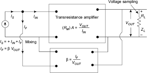
FIGURE 2 Block diagram of voltage shunt feedback amplifier

FIGURE 3 Transconductance amplifier (current series feedback amplifier)

FIGURE 4 Block diagram of current shunt feedback amplifier
Example 16 Discuss the advantages and disadvantages of negative feedback in amplifiers.
- Reduction of frequency and phase distortion
(Wave form distortion due to the non-linearity of the active device characteristics)
Voltage gain of negative feedback amplifier AN.F.B =

If the amplifier gain is very large so that Aβ >> 1; AN.F.B ≅
 (1)
(1)Now, the gain ANFB of the feedback amplifier is independent of the gain A of the internal amplifier in the forward path. The equation (1) means that the negative feedback in amplifiers has brought the amplifier out of the many inherent disadvantages as discussed below. The sacrifice in gain has brought many of the following advantages for a better performance of the negative feedback amplifier.
Under these conditions the overall gain of negative feedback amplifier is purely dependent upon β of the feedback network. And as such, any changes in the active device parameters, ageing and temperature changes, and supply voltage fluctuations do not have any effect on the gain of negative feedback amplifiers also. If the feedback network contains only resistive elements the gain becomes independent of frequency. So, there is substantial reduction in the frequency and phase shift distortion. In addition, passive components, the capacitors and resistors with high precision can be used in the feedback path to stabilise the response of negative feedback amplifiers. Thus, the stabilisation of amplifier gain is achieved.
- Nonlinear distortion due to second harmonic distortion in large signal amplifiers is reduced by the factor D = [1 + Aβ] as shown by the following equation
- Fractional change in gain A is reduced by the desensitivity factor D. Changes in output voltages or currents are feedback inputs and as such error changes in opposite direction effecting the output to be independent of changes in the basic amplifier gain. Thus, the overall stability is improved against parameter changes in a negative feedback amplifier.
- The input impedance ZIN, output impedance ZOUT of the amplifiers can be modified with the introduction of negative feedback into the amplifiers depending upon the requirements for improved responses and performances of the amplifiers.
- The amplifier bandwidth of the negative feedback amplifier almost equal to the high frequency cut-off f2f is increased due to the reduction in amplifier gain, because the product of the gain and the amplifier bandwidth is constant. So, there is an improvement in the amplifier responses with increased bandwidth and stability in gain and operation
f2.F.B = f2.[1 + β.Am]
- The gain bandwidth product of the amplifier is unaltered.
- Disadvantage: The gain gets reduced with negative feedback. As the advantages overweigh the disadvantages, negative feedback is extensively used in negative feedback amplifiers, complex control systems, robotics, mechatronics, econometrics and modelling.
Example 17: Mention the various types of negative feedback amplifiers and draw their equivalent circuits for the four categories of feedback amplifiers.
- Voltage series feedback amplifier
- Voltage shunt feedback amplifier
- Current series feedback amplifier
- Current shunt feedback amplifier
- Voltage series feedback amplifier-equivalent circuit
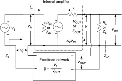
FIGURE 1 Voltage series feedback amplifier-equivalent circuit
- Voltage shunt feedback amplifier–equivalent circuit
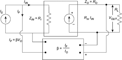
FIGURE 2 Equivalent circuit representing voltage shunt feedback amplifier
- Current series feedback amplifier-equivalent circuit
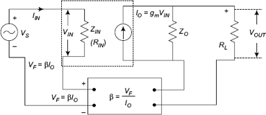
FIGURE 3 Equivalent circuit representing a curent series feedback amplifier
- Current shunt feedback amplifier circuit-equivalent circuit

FIGURE 4 Current shunt feedback amplifier-equivalent circuit
Questions for Practice
- Derive the expression for AV.f, RO.f, Ri.f, for voltage series feedback amplifiers.
- With circuit diagram explain how voltage series and voltage shunt feedback are obtained in a common emitter transistor amplifier.
- Explain the schematic detail of a single loop feedback amplifier and obtain the expression for gain with feedback Af. Mention the advantages of negative feedback.
- Show that the gain bandwidth product of an amplifier with negative feedback is the same that of an amplifier without feedback.
- Draw the circuit diagram of an emitter follower. Explain its working. List its important characteristics. Show how it performs the function of impedance transformation.
- Write short notes on the concept of negative feedback in amplifier circuits.
- Discuss the effect of negative feedback on noise in amplifiers.
- How does negative feedback stabilise the quiescent operating point of an amplifier.
- Discuss the effect of voltage series feedback on input impedance of an amplifier.
- Discuss the effect of current series feedback on output impedance of an amplifier.
- Discuss the effect on reduction of harmonic distortion with negative feedback.
- Draw the block diagrams for the four types of negative feedback amplifiers illustrating the sampling of signals at the output port and mixing of signals at the input port.
- Draw the four block diagrams illustrating the equivalent circuits for the four categories of negative feedback amplifiers.
- Mention the magnitudes of input and output impedances of negative feedback amplifiers and how they are modified from the input and output impedances of normal amplifiers.
- Draw the voltage series feedback amplifier circuit. Substantiate the method of sampling and the nature of feedback. Derive the expressions for voltage gain, current gain, input impedance and output impedance of the circuit.
- Draw the voltage shunt feedback amplifier circuit. Substantiate the method of sampling and the nature of feedback. Derive the expressions for voltage gain, current gain, input impedance and output impedance of the circuit.
- Draw the current series feedback amplifier circuit. Substantiate the method of sampling and the nature of feedback. Derive the expressions for voltage gain, current gain, input impedance and output impedance of the circuit.
- Draw the current shunt feedback amplifier circuit. Substantiate the method of sampling and the nature of feedback. Derive the expressions for voltage gain, current gain, input impedance and output impedance of the circuit.
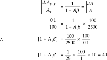
- For an amplifier having frequency response with the lower cut-off frequency f1 = 100 Hz and upper cut-of frequency f2 = 100 KHz, find the magnitude of Aβ so as to modify its frequency response using negative feedback with f1 = 10 Hz and f2 = 1 MHz.
- With the introduction of negative feedback into amplifiers, discuss the effect on the half-power frequencies of the frequency response of the amplifier and mention the reasons.
- Mention the type of feedback used to convert a non-ideal current amplifier into ideal current amplifier.
- Mention the type of feedback used to convert a non-ideal voltage amplifier into ideal voltage amplifier.
- If the output voltage of an amplifier is one volt before feedback, calculate the magnitude of the feedback factor to make the output voltage to 0.1 volt for an input signal of 10 mv.
- Mention the type of feedback amplifier with feedback factor β = 1.
- Mention the magnitude of voltage gain of a voltage series feedback amplifier.
- Using a block diagram illustrate the concepts of negative feedback and positive feedback into amplifiers. Also, derive the expressions for amplifier gains with feedback.
- Draw the frequency response characteristics of amplifiers with feedback and without feedback. Substantiate the concept of gain bandwidth product of amplifiers to be constant with necessary equations.
- Using a block diagram illustrate the concept of negative feedback and further explain the concept of voltage series feedback in amplifiers. Explain these concepts using appropriate transistor amplifier circuit or FET amplifier circuit.
- Using a block diagram illustrate the concept of negative feedback and further explain the concept of voltage shunt feedback in amplifiers. Explain these concepts using appropriate transistor amplifier circuit or FET amplifier circuit.
- Using a block diagram illustrate the concept of negative feedback and further explain the concept of current series feedback in amplifiers. Explain these concepts using appropriate transistor amplifier circuit or FET amplifier circuit.
- Using a block diagram illustrate the concept of negative feedback and further explain the concept of current shunt feedback in amplifiers. Explain these concepts using appropriate transistor amplifier circuit or FET amplifier circuit.
- Discuss the advantages of negative feedback amplifiers with necessary equations.
- Mention the main disadvantage of negative feedback amplifiers and discuss the various factors that form the foundation for the use of negative feedback amplifiers.
- Derive the expression for comparing the fractional change in gain of an amplifier with negative feedback and without feedback. Discuss the consequences.
- Draw the circuit of emitter follower. Discuss the nature of feedback that exists in the circuit. Derive the expressions for feedback factor β, voltage gain, input and output impedances. Discuss the application of the circuit as unity gain buffer amplifier.
- Draw the circuit of source follower. Discuss the nature of feedback that exists in the circuit. Derive the expressions for feedback factor β, voltage gain, input and output impedances. Discuss the application of the circuit as unity gain buffer amplifier.
- Draw a block diagram to illustrate the concept of the introduction of combined voltage and current feedback in the same amplifier circuit.
- The circuit alterations of a normal amplifier, which sample a portion of the output, signal whether voltage sampling or current sampling and return it to the input port cause for the development of negative feedback amplifiers. Discuss the various topologies that improve the performance of the open loop amplifier.
- The performance of transistor amplifiers is improved by returning a fraction of the output signal to the input port to form negative feedback. Discuss the various improvements or advantages of negative feedback amplifiers.
- Draw the circuit diagram of current shunt feedback amplifier using BJT and derive the expressions for feedback factor closed loop gain, input and output impedances.
Points to Remember
- The performance of transistor amplifiers is improved with some features by using negative feedback into the standard amplifiers.
- Alterations in some circuit features of a normal amplifier, which returns a sampled signal from its output port to the input port for causing effective changes in the input signal parameters so that the effective input signal is decreased forms negative feedback amplifier.
- By using a frequency selective feedback network the frequency response of an amplifier can be modified to the desired characteristic.
- Negative feedback is effective in reducing distortion in amplifiers.
- The stability of operation of feedback amplifiers is improved by making the closed loop gain of a negative feedback amplifier much greater than unity so that the gain of the feedback amplifier is dependent on the circuit components of the feedback network. Further, any drifts or changes in the parameters of active device do not have any effect on the performance of negative feedback amplifiers as the gain of negative feedback amplifier Af = (β)−1.
- The feedback voltage is 180° out of phase with the input signal for providing negative feedback in amplifier circuits. That is the reason why common emitter transistor amplifiers or common source FET amplifiers find their use in negative feedback systems.
- From the concept of constant gain bandwidth product of amplifiers, the reduction in gain of negative feedback amplifiers compensates by improved frequency response or bandwidth of the feedback amplifiers.
- In feedback amplifiers part of the output is mixed or combined with the input depending on the modifications of circuit features, for example, increase in output impedance is achieved by current sampling at the output port of the amplifier.
- Loop gain Aβ is the product of the gain of the signal undergone in the forward path, the forward gain A and the feedback factor β back through the feedback path.
- The ratio of the fractional change in gain of feed back amplifier to the fractional change in gain of normal amplifier is [1 + Aβ]−1.
- The overall behaviour or performance of negative feedback amplifier depends on the nature of components used in the feedback network.
- Feedback amplifiers maintain stable output irrespective of the variations in the forward path due to variations in device parameters with changes in temperature or so.
- Distortion in the output of feedback amplifiers is reduced by the factor [1 + Aβ]−1.
- The upper 3-db frequency of feedback amplifier is increased by the factor [1 + Aβ].
- A transresistance amplifier is known as current-voltage converter.
- A transconductance amplifier is known as voltage-current converter.
- Series feedback to the input port increases the input impedance of the amplifier.
- Shunt feedback to the input port decreases the input impedance of the amplifier.
- Voltage sampling at the output port of the amplifier reduces the output impedance.
- Current sampling at the output port of the amplifier increases the output impedance.
- There are four types of negative feedback amplifiers:
- Voltage series feedback amplifier
- Current series feedback amplifier
- Voltage shunt feedback amplifier
- Current shunt feedback amplifier
- The voltage gain AVNFB of a negative feedback amplifier is equal to
 , where A is the gain of the internal amplifier and β is the feedback factor. So, the gain of an amplifier decreases with an introduction of negative feedback into the circuit.
 - If the feedback quantity is to be connected in series, the quantity should always be voltage, that is Vf, irrespective of whether the parameter is voltage or current.
- If the feedback quantity is to be connected into the input port in shunt, then it should always be current, that is If, irrespective of voltage or current sampling being done.