
19
BIOS/UEFI FORENSICS: FIRMWARE ACQUISITION AND ANALYSIS APPROACHES

Recent rootkits targeting UEFI firmware have renewed interest in UEFI firmware forensics. Leaks of classified information on state-sponsored BIOS implants, as well as the security breach at Hacking Team mentioned in Chapter 15, have demonstrated the increasingly stealthy and powerful capabilities of malware that targets the BIOS and prompted the research community to dig deeper into firmware. We’ve already discussed some technical details of these BIOS threats in previous chapters. If you haven’t read Chapters 15 and 16, we highly recommend doing so before continuing; those chapters cover important firmware security concepts that we assume you understand for this discussion.
NOTE
In this chapter, we use the terms BIOS and UEFI firmware interchangeably.
UEFI firmware forensics is currently an emerging area of research, so security researchers working in this field lack conventional tools and approaches. In this chapter, we’ll cover some firmware analysis techniques, including various approaches to firmware acquisition and methods of parsing and extracting useful information.
We first focus on acquiring firmware, which is usually the first step of a forensic analysis. We cover both a software and a hardware approach to obtaining a UEFI firmware image. Next, we compare these approaches and discuss the advantages and disadvantages of each. We then discuss the internal structure of the UEFI firmware image and how to parse it in order to extract forensic artifacts. In the context of this discussion, we show you how to use UEFITool, an indispensable open source firmware analysis tool for browsing and modifying UEFI firmware images. Finally, we discuss Chipsec, a tool with very extensive and powerful functionality, and consider its applications for forensics analysis. Both tools were introduced in Chapter 15.
Limitations of Our Forensic Techniques
The material we present here does have some limitations. In modern platforms, there are many types of firmware: UEFI firmware, Intel ME firmware, hard drive controller firmware, and so on. This chapter is dedicated specifically to the analysis of UEFI firmware, which constitutes one of the largest parts of platform firmware.
Note also that firmware is very platform specific; that is, each platform has its own peculiarities. In this chapter, we’ll focus on UEFI firmware for Intel x86 systems, which constitute the majority of desktop, laptop, and server market segments.
Why Firmware Forensics Matter
In Chapter 15, we saw that modern firmware is a convenient place for embedding very powerful backdoors or rootkits, specifically in the BIOS. This type of malware is capable of surviving OS reinstallation or hard drive replacement, and it gives an attacker control over an entire platform. At the time of this writing, most state-of-the-art security software doesn’t take into account UEFI firmware threats at all, making them even more dangerous. This gives an attacker a big opportunity to implant malware that persists undetected on the target system.
Next, we outline a couple of specific ways attackers might use firmware rootkits.
Attacking the Supply Chain
Threats targeting UEFI firmware increase the risk of supply chain attacks, because attackers can install a malicious implant on a server before it is delivered to the data center or to a laptop before it gets to the IT department. And because these threats can impact a large number of a service provider’s clients by exposing all their secrets, big cloud-computing players like Google have recently started to use firmware forensic analysis techniques to ensure that their firmware isn’t compromised.
Compromising BIOS Through Firmware Vulnerability
Attackers can compromise the platform firmware by exploiting a vulnerability in it to bypass BIOS write protection or authentication. For a refresher on this attack, return to Chapter 16, where we discuss different classes of vulnerabilities used to attack the BIOS. To detect these attacks, you could use the firmware forensic approaches discussed in this chapter to verify the integrity of a platform’s firmware or to help detect malicious firmware modules.
Understanding Firmware Acquisition
The very first step in BIOS forensic analysis is the process of obtaining an image of the BIOS firmware to analyze. To better understand the location of BIOS firmware on modern platforms, refer to Figure 19-1, which demonstrates the architecture of a typical PC system’s chipset.
There are two main components in the chipset: a CPU and a Platform Controller Hub (PCH) or South Bridge. The PCH provides a connection between the controllers of peripheral devices available on the platform and the CPU. In most modern systems based on Intel x86 architecture (including 64-bit platforms), the system firmware is located on a flash memory in the Serial Peripheral Interface (SPI) bus ➊, which is physically connected to the PCH. The SPI flash constitutes the main target for forensic analysis because it stores the firmware we want to analyze.

Figure 19-1: A block diagram of a modern Intel chipset
The motherboard of a PC typically has one discrete physical SPI flash chip soldered onto it, but you might occasionally encounter systems with multiple SPI flash chips. This happens when a single chip doesn’t have enough capacity to store all the system firmware; in that case, the platform vendor uses two chips. We discuss this situation later in this chapter, in “Locating the SPI Flash Memory Chip” on page 376.
To acquire the firmware image stored on the SPI flash, you need to be able to read the contents of the flash. Generally speaking, you can read the firmware using either a software or a hardware approach. In the software approach, you attempt to read the firmware image by communicating with the SPI controller using software running on the host CPU. In the hardware approach, you physically attach a special device called an SPI programmer to the SPI flash, then read the firmware image directly from the SPI flash. We’ll cover both approaches, starting with the software method.
Before we go into the description of the software approach, however, you should understand that each approach has its advantages and limitations. One of the benefits of dumping UEFI firmware using the software method is that you can do it remotely. A user of the target system can run an application to dump the contents of the SPI flash and send it to a forensic analyst. But this approach also has a major drawback: if an attacker has already compromised the system firmware, he or she could interfere with the process of firmware acquisition by forging the data read from the SPI flash. This makes the software approach somewhat unreliable.
The hardware approach doesn’t have the same drawback. Even though you must be physically present and it requires you to open the target system’s chassis, this method directly reads the contents of the powered-off system’s SPI flash without giving the attacker any opportunity to counterfeit the data (unless you’re dealing with a hardware implant, which we don’t cover in this book).
The Software Approach to Firmware Acquisition
In the software approach to dumping UEFI firmware from the target system, you read the contents of the SPI flash from the operating system. You can access modern systems’ SPI controllers through registers in the PCI configuration space (a block of registers that specify device configuration on the PCI bus). These registers are memory mapped, and you can read and write to them using regular memory read and write operations. In this section, we’ll demonstrate how to locate these registers and communicate with the SPI controller.
Before we proceed, you should know that the location of an SPI register is chipset specific, so in order to communicate with an SPI controller, we need to refer to the chipset dedicated to the platform we’re targeting. In this chapter, we’ll demonstrate how to read the SPI flash on chipsets in Intel’s 200 Series (the location of SPI registers can be found at https://www.intel.com/content/www/us/en/chipsets/200-series-chipset-pch-datasheet-vol-2.html), which are the latest chipsets for desktop systems at the time of this writing.
It’s also worth mentioning that the memory locations that correspond to the registers exposed via the PCI configuration space are mapped in the kernel-mode address space and, as a result, aren’t accessible to code running in the user-mode address space. You would need to develop a kernel-mode driver to access the address range. The Chipsec tool discussed later in this chapter provides its own kernel-mode driver for accessing the PCI configuration space.
Locating PCI Configuration Space Registers
First we need to locate the memory range where the SPI controller’s registers are mapped. This memory range is called the Root Complex Register Block (RCRB). At offset 3800h in the RCRB, you’ll find the SPI Base Address Register (SPIBAR), which holds the base address of memory-mapped SPI registers (see Figure 19-2).
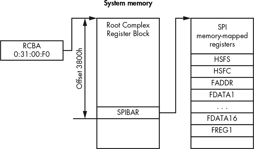
Figure 19-2: The location of SPI control and status registers in system memory
The RCRB address is stored in the Root Complex Base Address (RCBA) PCI register, which is located on bus 0, device 31h, function 0. This is a 32-bit register, and the address of the RCRB is provided in bits 31:14. We assume that the lower 14 bits of the RCRB’s address are zeros, since RCRB is aligned at the boundary of 16Kb. Once we get the RCRB’s address, we can obtain the SPIBAR value by reading memory at the 3800h offset. In the next section, we discuss the SPI registers in more detail.
Calculating SPI Configuration Register Addresses
Once we’ve obtained the SPIBAR value, which provides us with the location of the SPI registers in memory, we can program the registers to read the contents of an SPI flash. The offsets of the SPI registers may vary depending on the platform, so the best way to determine the actual values for a given hardware configuration is to look up the values in the platform chipset documentation. For instance, for platforms supporting Intel’s latest CPU at the time of this writing (Kaby Lake), we can consult the Intel 200 Series Chipset Family Platform Controller Hub datasheet to find the location of the SPI memory-mapped registers. The information is in the section called “Serial Peripheral Interface.” For each SPI register, the datasheet provides its offset from the SPIBAR value, register name, and the register default value at the platform reset. We’ll use this datasheet as a reference in this section to determine the addresses of the SPI registers we’re interested in.
Using the SPI Registers
Now that you know how to find the addresses of SPI registers, you can figure out which one you’ll use to read the contents of the SPI flash. Table 19-1 lists all the registers we’ll need to obtain an image of the SPI flash.
Table 19-1: SPI Registers for Firmware Acquisition
Offset from SPIBAR |
Register name |
Register description |
04h–05h |
HSFS |
Hardware sequencing flash status |
06h–07h |
HSFC |
Hardware sequencing flash control register |
08h–0Bh |
FADDR |
Flash address |
10h–4Fh |
FDATAX |
Array of flash data |
58h–5Bh |
FREG1 |
Flash region 1 (BIOS descriptor) |
We’ll discuss each of these registers in the following sections.
The FREG1 Register
The register we’ll start with is flash region 1 (FREG1). It provides the location of the BIOS region on the SPI flash. The layout of this 32-bit-length register is presented in Figure 19-3.

Figure 19-3: The layout of FREG1 SPI register
The Region Base field ➋ provides 24:12 bits of the base address for the BIOS region in the SPI flash. Since the BIOS region is aligned at 4Kb, the lowest 12 bits of the region’s base address start at 0. The Region Limit field ➊ provides 24:12 bits for the BIOS region in the SPI flash. For instance, if the Region Base field contains a value of 0xaaa and Region Limit contains a value of 0xbbb, then the BIOS regions spans from 0xaaa000 to 0xbbbfff on the SPI flash.
The HSFC Register
The hardware sequencing flash control (HSFC) register allows us to send commands to the SPI controller. (In the specification, these commands are referred to as cycles.) You can see the layout of the HSFC register in Figure 19-4.

Figure 19-4: The layout of HSFC SPI register
We use the HSFC register to send a read/write/delete cycle to the SPI flash. The 2-bit FCYCLE field ➌ encodes the operation to perform the following:
00 Read a block of data from the SPI flash
01 Write a block of data to the SPI flash
11 Erase a block of data on the SPI flash
10 Reserved
For read and write cycles, the FDBC field ➋ indicates the number of bytes that should be transferred to and from the SPI flash. The content of this field is zero based; a value of 000000b represents 1 byte, and a value of 111111b represents 64 bytes. As a result, the number of bytes to transfer is the value of this field plus 1.
The FGO field ➍ is used to initiate the SPI flash operation. When the value of this field is 1b, the SPI controller will read, write, and erase the data based on the values written to the FCYCLE and FDBC fields. Before setting the FGO field, the software needs to have specified all the registers that indicate the type of the operation, the amount of data, and the SPI flash address.
The final HSFC field that deserves our attention is flash SPI SMI# enable (FSMIE) ➊. When this field is set, the chipset generates a System Management Interrupt (SMI), which leads to the execution of the SMM code. As we’ll see in “Considering the Drawbacks of the Software Approach” on page 373, you could use FSMIE to counteract the firmware image acquisition.
The FADDR Register
We use the flash address (FADDR) register to specify the SPI flash linear address for read, write, and erase operations. This register is 32 bits, but we use only the lower 24 bits to specify a linear address for the operation. The upper 8 bits of this register are reserved and unused.
The HSFS Register
Once we’ve initiated the SPI cycle by setting the FGO field of the HSFC register, we can determine when the cycle has finished by looking at the hardware sequencing flash status (HSFS) register. This register is composed of multiple fields that provide information on the status of the requested operation. In Table 19-2, you can see the HSFS fields used to read the SPI image.
Table 19-2: The SPI Register HSFS Fields
Field offset |
Field size |
Field name |
Field description |
0h |
1 |
FDONE |
Flash cycle done |
1h |
1 |
FCERR |
Flash cycle error |
2h |
1 |
AEL |
Access error log |
5h |
1 |
SCIP |
SPI cycle in progress |
The FDONE bit is set by the chipset when the previous flash cycle (initiated by the HSFC register’s FGO field) is complete. The FCERR and AEL bits indicate that an error has occurred during the SPI flash cycle and that the returned data may not contain valid values, respectively. The SCIP bit indicates that the flash cycle is in progress. We set the SCIP by setting the FGO bit, and the SCIP clears when the value of FDONE is 1. Based on this information, we can determine that the operation we initiated has completed successfully when the following expression is true:
(FDONE == 1) && (FCERR == 0) && (AEL == 0) && (SCIP == 0)
The FDATAX Registers
The array of flash data (FDATAX) registers hold the data to be read from or written to the SPI flash. Each register is 32 bits, and the total number of FDATAX registers in use depends on the amount of bytes to transfer, which is specified in the HSFC register’s FDBC field.
Reading Data from the SPI Flash
Now let’s put together all this information and see how to read data from the SPI flash using these registers. First, we locate the Root Complex Registers Block, from which we can determine the base address of SPI memory-mapped registers and get access to those registers. By reading the FREG1 SPI register, we can determine the location of the BIOS region on the flash—that is, the BIOS starting address and BIOS limit.
Next, we read the BIOS region using the SPI registers just described. This step is demonstrated in Figure 19-5.

Figure 19-5: Reading data from the SPI flash
First, we set FADDR to the linear address of the flash memory region that we want to read ➊. Then we specify the total number of bytes to read from flash memory by setting the FDBC field ➋ of the flash control register. (A value of 111111b would read 64 bytes per cycle.) Next we set the FCYCLE field ➌ with the 00b value, which indicates the read cycle and sets the FGO bit ➍ that starts our flash reading operation.
Once we set the FGO bit, we need to monitor the flash status register to know when the operation is complete. We can do this by checking the FDONE, FCERR, AEL, and SCIP fields ➎. Once the read operation is finished, we read flash data from the FDATAX registers ➏. The FDATAX[1] register provides us with the first 4 bytes of flash memory at the target address specified in the FADDR register; FDATAX[2] provides us with the second 4 bytes of flash memory, and so on. By repeating these steps and incrementing the FADDR value by 64 bytes in each iteration, we read the whole BIOS region from the SPI flash.
Considering the Drawbacks of the Software Approach
The software approach to BIOS firmware dumping is convenient because it doesn’t require you to be physically present; with this method, you can read the contents of the SPI flash remotely. But it isn’t robust against an attacker who has already compromised the system firmware and can execute malicious code in SMM.
As we’ve noted, the HSFC register has an FSMIE bit that triggers an SMI when the flash cycle completes. If an attacker has already compromised SMM and is able to set the FSMIE bit before the firmware acquisition software sets the FGO bit, then the attacker will receive control once the SMI is generated and will be able to modify the contents of the FDATAX registers. As a result, the firmware acquisition software will read forged values from FDATAX and won’t be able to get an original image of the BIOS region. Figure 19-6 demonstrates this attack.

Figure 19-6: Subverting a software BIOS acquisition via SMI
Before the reader sets the FGO bit ➋ in the flash control register, the attacker writes 1 to the register’s FSMIE bit ➊. Once the cycle is finished and data is written back to the FDATAX registers, an SMI is triggered and the attacker receives control ➌. Then the attacker modifies the contents of the FDATAX registers ➍ to conceal the attack on the BIOS firmware. After regaining control, the reader will receive fake data ➎ and won’t detect the compromised firmware.
This attack demonstrates that the software approach doesn’t provide a 100 percent reliable solution for firmware acquisition. In the following section, we’ll discuss the hardware approach to obtaining system firmware for forensic analysis. Conducting forensic analysis by physically attaching a device to the SPI flash avoids the possibility of the attack depicted in Figure 19-6.
The Hardware Approach to Firmware Acquisition
To guarantee we have acquired the actual BIOS image stored on the SPI flash and not one already compromised by an attacker, we can use the hardware approach. With this approach, we physically attach a device to the SPI flash memory and read its contents directly. This is the best solution because it’s more trustworthy than the software approach. As an extra benefit, this approach allows us to obtain other firmware stored on the SPI flash, like ME and GBE firmware, which might not be accessible with the software approach due to restrictions enforced by the SPI controller.
The SPI bus on modern systems allows multiple masters to communicate with the SPI flash. For instance, on systems based on the Intel chipset, there are generally three masters: the host CPU, the Intel ME, and GBE. These three masters have different access rights to different regions of the SPI flash. On most modern platforms, the host CPU can’t read and write to the SPI flash region containing the Intel ME and GBE firmware.
Figure 19-7 demonstrates a typical setup for obtaining the BIOS firmware image by reading the SPI flash.

Figure 19-7: A typical setup for dumping the SPI flash image
In order to read data from the flash memory, we need an additional device, called an SPI programmer, which we physically attach to the SPI flash memory chip on the target system. We also connect the SPI programmer via a USB or UART interface to a host that we use to obtain the BIOS firmware image. We would then run some particular software on the programmer to make it read data from the flash memory chip and transfer the data to the analyst’s computer. This might be proprietary software provided with a particular SPI programmer, or it could be an open source solution such as the Flashrom tool, which is discussed later in “Reading the SPI Flash with the FT2232 Mini Module” on page 377.
Reviewing a Lenovo ThinkPad T540p Case Study
The hardware approach is even more specific than the software approach. It requires you to consult platform documentation in order to learn what kind of flash memory the platform uses to store the firmware and where the firmware is physically located in the system. In addition, there are numerous flash programming devices for specific hardware we could use to read the contents of the flash memory. We won’t discuss the various hardware and software options available for system firmware acquisition, because there are simply too many. Instead, we’ll go over one of the possible ways to dump firmware from the Lenovo ThinkPad T540p using the FT2232 SPI programmer.
We chose this SPI programmer because of its relatively low price (about $30) and flexibility, as well as our prior experience of working with it. As we’ve mentioned, there are many solutions, and each has its unique features, advantages, and drawbacks.
Another device we’d like to mention is the Dediprog SF100 ISP IC Programmer (shown in Figure 19-8). It’s popular in the security research community, supports many SPI flashes, and offers extensive functionality. Minnowboard, an open source reference board for hardware and firmware developers, has a good tutorial on using Dediprog for updating firmware at https://minnowboard.org/tutorials/updating-firmware-via-spi-flash-programmer/.

Figure 19-8: A Dediprog SF100 ISP IC Programmer
Locating the SPI Flash Memory Chip
Let’s start by physically reading the firmware image from the Lenovo ThinkPad T540p platform. First, to dump the system firmware from the target system, we need to find where, on the main board, the SPI flash memory chips are located. To do this, we consulted the Hardware Maintenance Manual (https://thinkpads.com/support/hmm/hmm_pdf/t540p_w540_hmm_en_sp40a26003_01.pdf) for this laptop model and took apart the target system’s hardware. In Figures 19-9 and 19-10, you can see the locations of the two flash memory chips. Figure 19-9 shows a complete image of the system board. The SPI flash chips are located in the highlighted area.
WARNING
Don’t repeat the actions described in this section unless you are 100 percent sure of what you’re doing. An invalid or incorrect configuration of the tools may brick the target system.

Figure 19-9: The Lenovo ThinkPad T540p mainboard with SPI flash modules
Figure 19-10 zooms in on the region highlighted in Figure 19-9 so you can see the SPI flash chips more clearly. This laptop model uses two SOIC-8 flash memory modules to store the firmware—a 64Mb (8MB) one and a 32Mb (4MB) one. This is a very popular solution on many modern desktops and laptops.

Figure 19-10: The location of the SPI flash modules on the mainboard of the laptop
Since two separate chips are used to store the system firmware, we’ll need to dump the contents of both. We’ll obtain the final firmware image by concatenating the images from the two flash memory chips into a single file.
Reading the SPI Flash with the FT2232 Mini Module
Once we’ve identified the physical location of the chips, we can connect the SPI programmer’s pins to the flash module on the system board. The datasheet (http://www.ftdichip.com/Support/Documents/DataSheets/Modules/DS_FT2232H_Mini_Module.pdf) for the FT2232H Mini Module shows us which pins we should use to attach the device to the memory chip. Figure 19-11 demonstrates the layout of the pins for both the FT2232H Mini Module and the SPI flash chip.
The FT2232H has two sets of pins, corresponding to two channels: Channel 2 and Channel 3. You may use either channel to read the contents of the SPI flash memory. In our experiment, we use Channel 3 to attach the FT2232H to the SPI memory chip. Figure 19-11 shows which of the FT2232H pins we connected to the corresponding pins of the SPI flash memory chip.
In addition to connecting the FT2232H to the memory chip, we need to configure it to operate in USB bus-powered mode. The FT2232H Mini Module supports two modes of operating: USB bus-powered and self-powered. In the bus-powered mode, the mini module takes power from the USB bus it is attached to, and in self-powered mode, the power is provided independently of the USB bus connection.

Figure 19-11: The layout of the pins for the FT2232H Mini Module and SPI flash chip
To help us attach our SPI programmer to the SPI chip module, we use a SOIC-8 clip, as shown in Figure 19-12. This clip allows us to easily connect the mini module’s pins to the corresponding pins of the flash memory chip.

Figure 19-12: Attaching the FT2232H Mini Module to the SPI flash chip
Once we connect all the components, we can read the contents of the SPI flash chip. To do this, we use an open source tool called Flashrom (https://www.flashrom.org/Flashrom). This tool was developed specifically for identifying, reading, writing, verifying, and erasing flash chips. It supports a large number of flash chips and works with many different SPI programmers, including the FT2232H Mini Module.
Listing 19-1 shows the results of running Flashrom to read the contents of both SPI flash chips on the Lenovo ThinkPad T540p platform.
➊ user@host: flashrom -p ft2232_spi:type=2232H,port=B --read dump_1.bin
flashrom v0.9.9-r1955 on Linux 4.8.0-36-generic (x86_64)
flashrom is free software, get the source code at https://flashrom.org
Calibrating delay loop... OK.
➋ Found Macronix flash chip "MX25L6436E/MX25L6445E/MX25L6465E/MX25L6473E"
(8192 kB, SPI) on ft2232_spi.
➌ Reading flash... done.
user@host: flashrom -p ft2232_spi:type=2232H,port=B --read dump_2.bin
flashrom v0.9.9-r1955 on Linux 4.8.0-36-generic (x86_64)
flashrom is free software, get the source code at https://flashrom.org
Calibrating delay loop... OK.
Found Macronix flash chip "MX25L3273E" (4096 kB, SPI) on ft2232_spi.
Reading flash... done.
➍ user@host: cat dump_2.bin >> dump_1.bin
Listing 19-1: Dumping SPI flash images with the Flashrom tool
First, we run Flashrom to dump the contents of the first SPI flash chip, passing it a programmer type and port number as parameters ➊. The type we specify, 2232H, corresponds to our FT2232H Mini Module, and port B corresponds to Channel 3, the one we’re using to connect to the SPI flash chip. The --read parameter tells Flashrom to read the contents of the SPI flash memory into the dump_1.bin file. Once we run the tool, it displays the type of the detected SPI flash chip—in our case, Macronix MX25L6473E ➋. Once Flashrom finishes reading the flash memory, it outputs a confirmation ➌.
After reading the first flash chip, we reconnect the clip to the second chip and run Flashrom again to dump the second chip’s contents into the dump_2.bin file. Once this operation is done, we create a complete image of the firmware by concatenating the two dumped images ➍.
We have now dumped a complete, trustworthy image of the firmware. Even if the BIOS is already infected and an attacker attempts to thwart our firmware acquisition, we’ll still obtain the actual firmware code and data. Next, we’ll analyze it.
Analyzing the Firmware Image with UEFITool
Once we obtain a firmware image from the target system’s SPI flash, we can analyze it. In this section, we’ll cover the basic components of platform firmware, such as firmware volumes, volume files, and the sections necessary for understanding the layout of the UEFI firmware in the flash image. Then we’ll focus on the most important steps in the forensic analysis of firmware.
NOTE
In this section, we’ll provide high-level descriptions rather than detailed definitions of the data structures used, since this is too large a subject and in-depth coverage is beyond the scope of this chapter. We will, however, provide references to documentation containing definitions and the layout of the data structures if you’d like further information.
We’re going to revisit UEFITool (https://github.com/LongSoft/UEFITool/), the open source tool for parsing, extracting, and modifying UEFI firmware images that was introduced in Chapter 15, to demonstrate theoretical concepts with the real firmware image we acquired in the previous section. The ability to look inside the firmware image to browse and extract various components is incredibly useful for forensic analysis. This tool doesn’t require installation; once downloaded, the application is ready to be executed.
Getting to Know the SPI Flash Regions
Before we look at the firmware image, we need to go over how the information stored on the SPI flash is organized. Generally, modern platforms based on the Intel chipset SPI flash consist of several regions. Each region is dedicated to storing firmware for a specific device available in the platform; for instance, UEFI BIOS firmware, Intel ME firmware, and Intel GBE (integrated LAN device) firmware are each stored in their own region. Figure 19-13 demonstrates the layout of several regions of the SPI flash.

Figure 19-13: Regions of the SPI flash image
The SPI flash in modern systems supports up to six regions, including the descriptor region, where flash images always start. The descriptor region contains information about the SPI flash’s layout; that is, it provides the chipset with information about the other regions present on the SPI flash, such as their location and access rights. The descriptor region also dictates the access rights of each master in the system that can communicate with the SPI flash controller. Multiple masters are able to communicate with the controller at the same time. We can find the complete layout of the descriptor region, including definitions of all the data structures located in it, in the chipset specification for the target platform.
In this chapter, we’re primarily interested in the BIOS region, which contains firmware executed by the CPU at the reset vector. We can extract the location of the BIOS region from the descriptor region. Normally, BIOS is the last region on the SPI flash, and it constitutes the main target for forensic analysis.
Let’s take a look at the different regions of the SPI image that we acquired with the hardware approach.
Viewing SPI Flash Regions with UEFITool
First, launch UEFITool and select File▸Open image file. Then select the file with the SPI image you want to analyze—we’ve supplied one you can use with the book’s resources at https://nostarch.com/rootkits/. Figure 19-14 shows the result of this operation.

Figure 19-14: Browsing SPI flash regions in UEFITool
When the firmware image loads, UEFITool automatically parses it and provides this information in a tree-like structure. In Figure 19-14, the tool identified that the firmware image is from a system based on the Intel chipset ➊ with only four SPI regions: descriptor, ME, GbE, and BIOS. If we select the BIOS region in the Structure window, we can see information about it in the Information window. UEFITool shows the following items describing the region:
Offset ➋ The offset of the region from the beginning of the SPI flash image
Full size ➌ The size of the region in bytes
Memory address ➍ The address of the region mapped into the physical memory
Compressed ➎ Whether the region contains compressed data
The tool provides a convenient method for extracting individual regions (and any other object shown in the structure window) from the SPI image and saving them in a separate file, as shown in Figure 19-15.

Figure 19-15: Extracting a BIOS region and saving it as a separate file
To extract and save a region, right-click the region and select Extract as is . . . in the context menu. The tool will then show a regular dialog that lets you choose where you want to save your new file. Once you’ve done this, check the location you chose to confirm that the operation was successful.
Analyzing the BIOS Region
Once we’ve identified the location of the BIOS region, we can proceed with our analysis. At a high level, the BIOS region is organized into firmware volumes, which are basic storage repositories for data and code. The exact definition of the firmware volume is provided in the EFI Firmware Volume Specification (https://www.intel.com/content/www/us/en/architecture-and-technology/unified-extensible-firmware-interface/efi-firmware-file-volume-specification.html). Every volume starts with a header that provides the necessary volume attributes, such as the type of the volume filesystem, the volume size, and the checksum.
Let’s examine the firmware volumes available in the BIOS we’ve acquired. If we double-left-click the BIOS region in the UEFITool window (as in Figure 19-15), we get a list of firmware volumes available, as shown in Figure 19-16.

Figure 19-16: Browsing the firmware volumes available in the BIOS region
There are four firmware volumes available in our BIOS region, and you’ll also notice two regions marked Padding. The padding regions don’t belong to any of the firmware volumes but rather represent empty space between them, filled with either 0x00 or 0xff values depending on the erase polarity of the SPI flash. Erase polarity determines values written to flash memory for erase operation. If erase polarity is 1, then erased bytes of the flash memory are set to the values of 0xff; if erase polarity is 0, then erased bytes are set to 0x00. As a result, when erase polarity is 1, the padding regions (the empty space) consists of 0xff values.
In the information tab to the right of the volumes in Figure 19-16, we can see the attributes of the selected volume. Here are some of the important fields:
Offset ➊ The offset of the firmware volume from the beginning of the SPI image.
Signature ➋ The signature of the firmware volume in the header. This field is used to identify volumes in the BIOS regions.
Filesystem GUID ➌ The identifier of the filesystem used in the firmware volume. This Globally Unique Identifier (GUID) is displayed as the name of the volume in the structure window. If the GUID is documented, UEFITool displays its human-readable name (such as EfiFirmwareFileSystemGuid in Figure 19-16) instead of the hexadecimal value.
Header size ➍ The size of the firmware volume header. The volume data follows the header.
Body size ➎ The size of the firmware volume body—that is, the size of the data stored in the volume.
Getting to Know the Firmware Filesystem
The firmware volumes are organized as a filesystem, the type of which is indicated in a filesystem GUID in the firmware header. The filesystem most frequently used in firmware volumes is the firmware filesystem (FFS), defined in the EFI FFS specification, but firmware volumes also use other filesystems, such as FAT32 or NTFS. We’ll focus on the FFS as it is the most common.
The FFS stores all the files in the root directory and contains no provision for any directory hierarchy. According to the EFI FFS specification, each file has an associated type, located in that file’s header, that describes the data stored in that file. Here is a list of some frequently encountered file types that may be useful in forensic analysis:
EFI_FV_FILETYPE_RAW A raw file—no assumptions should be made about the data stored in the file.
EFI_FV_FILETYPE_FIRMWARE_VOLUME_IMAGE A file that contains an encapsulated firmware volume. Even though FFS has no provision for directory hierarchy, we can use this file type to create a tree-like structure by encapsulating firmware modules in files.
EFI_FV_FILETYPE_SECURITY_CORE A file with code and data that is executed at the Security (SEC) phase of the boot process. The SEC phase is the very first phase of the UEFI boot process.
EFI_FV_FILETYPE_PEI_CORE An executable file that initiates the Pre-EFI Initialization (PEI) phase of the boot process. The PEI phase follows the SEC phase.
EFI_FV_FILETYPE_PEIM The PEI modules, which are files with code and data executed at the PEI phase.
EFI_FV_FILETYPE_DXE_CORE An executable file that initiates the Driver Execution Environment (DXE) phase of the boot process. The DXE phase follows the PEI phase.
EFI_FV_FILETYPE_DRIVER An executable file launched at the DXE phase.
EFI_FV_FILETYPE_COMBINED_PEIM_DRIVER A file with code and data that can be executed at both the PEI and DXE phases.
EFI_FV_FILETYPE_APPLICATION A UEFI application, which is an executable that can be launched at the DXE phase.
EFI_FV_FILETYPE_FFS_PAD A padding file.
Unlike the typical filesystems used in operating systems, where files have human-readable filenames, FFS files are identified by GUIDs.
Getting to Know File Sections
Most firmware files stored in the FFS consist of a single part or multiple discrete parts, called sections (although some files, such as EFI_FV_FILETYPE_RAW files, don’t contain any sections).
There are two types of sections: leaf sections and encapsulation sections. Leaf sections directly contain data, the type of which is determined by a section type attribute in the section header. Encapsulation sections contain file sections, which may contain either leaf sections or encapsulation sections. This means that one encapsulation section can contain a nested encapsulation section.
The following list describes some types of leaf sections:
EFI_SECTION_PE32 Contains a PE image.
EFI_SECTION_PIC Contains position-independent code (PIC).
EFI_SECTION_TE Contains a Terse Executable (TE) image.
EFI_SECTION_USER_INTERFACE Contains a user interface string. It is typically used to store a human-readable name for the file, in addition to the file GUID.
EFI_SECTION_FIRMWARE_VOLUME_IMAGE Contains an encapsulated firmware image.
And here are a couple of the encapsulation sections defined in the FFS specification:
EFI_SECTION_COMPRESSION Contains compressed file sections.
EFI_SECTION_GUID_DEFINED Encapsulates other sections with respect to an algorithm that is identified by the section GUID. This type is used for signed sections, for example.
These objects constitute the contents of the UEFI firmware on modern platforms. A forensic analyst must account for every component of the firmware, whether it is a section with executable code, like PE32, TE or PIC, or a data file with nonvolatile variables.
To better understand the concepts presented here, see Figure 19-17, which demonstrates the location of the CpuInitDxe driver in the firmware volume. This driver is responsible for CPU initialization at the DXE phase. We’ll go from the bottom to the top in the FFS hierarchy in order to describe its location in the firmware image.

Figure 19-17: The location of the CpuInitDxe driver in the BIOS region
The driver’s executable image is located in the PE32 image section ➐. This section, along with other sections that contain the driver name ➑, version ➒, and dependencies ➏, are located in the file with the GUID {62D171CB-78CD-4480-8678-C6A2A797A8DE} ➎. The file is part of the encapsulated firmware volume ➍ stored in the compressed section ➌. The compressed section is located in the {9E21FD93-9C72-4C15-8C4B-E77F1DB2D792} file ➋ of the firmware volume image type, which is stored in the top-level firmware volume ➊.
This example is primarily intended to demonstrate the hierarchy of objects that constitute the UEFI firmware, but this is just one possible approach to parsing it.
Now that we know how the BIOS region is organized, we’ll be able to navigate its hierarchy and search for various objects stored in the BIOS firmware.
Analyzing the Firmware Image with Chipsec
In this section, we’ll discuss firmware forensic analysis with the platform security assessment framework Chipsec (https://github.com/chipsec/), introduced in Chapter 15. In this section, we’ll explore the tool’s architecture in more detail; then, we’ll analyze some firmware, providing a few examples that demonstrate Chipsec’s functionality and utility.
The tool provides a number of interfaces for accessing platform hardware resources, like physical memory, PCI registers, NVRAM variables, and the SPI flash. These interfaces are very useful to forensic analysts, and we’ll look at them more seriously later in this section.
Follow the installation guide in the Chipsec manual (https://github.com/chipsec/chipsec/blob/master/chipsec-manual.pdf) to install and set up the tool. The manual also covers a multitude of functionality that you can use, but in this section, we’re focusing only on Chipsec’s forensic analysis capabilities.
Getting to Know the Chipsec Architecture
Figure 19-18 shows the tool’s high-level architecture.

Figure 19-18: The Chipsec tool’s architecture
At the bottom, we can see modules that provide access to system resources, such as memory-mapped IO address ranges, PCI configuration space registers, and physical memory. These are platform-dependent modules implemented as kernel-mode drivers and EFI native code. (Currently, Chipsec provides kernel-mode drivers for Windows, Linux, and macOS.) Most of the modules are written in C and are intended to execute in kernel mode or in the EFI shell.
NOTE
The UEFI Shell is a UEFI application that provides a command line interface for firmware, allowing us to launch UEFI applications and execute commands. We can use the UEFI Shell to retrieve information on the platform, view and modify boot manager variables, load UEFI drivers, and more.
On top of these low-level OS-dependent components is an OS-independent abstraction layer called OS Helper, comprising a number of modules that hide an OS-specific API for communicating with kernel-mode components from the rest of the application. The modules located at this level are implemented in Python. At the bottom, these modules interface with the kernel-mode components; at the top, they provide an OS-independent interface for another component, the hardware abstraction layer (HAL).
The HAL further abstracts the platform’s low-level concepts, like the PCI configuration registers and model-specific registers (MSRs), and it provides an interface for the Chipsec components located at the levels immediately above it: Chipsec Main and Chipsec Util. The HAL is also written in Python and relies on OSHelper to access the platform-specific hardware resources.
The two remaining components, located at the top of the architecture, provide the main functionality available to users. The first interface, Chipsec Main, is available through the chipsec_main.py Python script in the tool’s root folder. It allows us to execute tests that check the security configuration of certain platform aspects, run PoCs to test for the presence of vulnerabilities in system firmware, and more. The second interface, Chipsec Util, is available through the chipsec_util.py script. We can use it to run individual commands and access platform hardware resources to read the SPI flash image, dump the UEFI NVRAM variables, and so on.
We’re primarily interested in the Chipsec Util interface because it provides rich functionality for working with UEFI firmware.
Analyzing Firmware with Chipsec Util
You can find out the commands provided by Chipsec Util by running the chipsec_util.py script, located in the root directory of the tool’s repository, without specifying any arguments. Generally, commands are grouped into modules based on the platform hardware resources they work with. Here are some of the most useful modules:
acpi Implements commands for working with Advanced Configuration and Power Interface tables.
cpu Implements commands related to the CPU, such as reading configuration registers and obtaining information about the CPU.
spi Implements a number of commands for working with the SPI flash, like reading, writing, and erasing data. There is also an option for disabling BIOS write protection on systems with unlocked write protection (as discussed in Chapter 16).
uefi Implements commands for parsing UEFI firmware (the SPI flash BIOS region) to extract executables, NVRAM variables, and the like.
We can run chipsec_util.py command_name, where command_name is the name of the command we want to learn about, to output a description and usage information for that command. For instance, Listing 19-2 displays the output of chipsec_util.py spi.
################################################################
## ##
## CHIPSEC: Platform Hardware Security Assessment Framework ##
## ##
################################################################
[CHIPSEC] Version 1.3.3h
[CHIPSEC] API mode: using OS native API (not using CHIPSEC kernel module)
[CHIPSEC] Executing command 'spi' with args []
➊ >>> chipsec_util spi info|dump|read|write|erase|disable-wp
[flash_address] [length] [file]
Examples:
>>> chipsec_util spi info
>>> chipsec_util spi dump rom.bin
>>> chipsec_util spi read 0x700000 0x100000 bios.bin
>>> chipsec_util spi write 0x0 flash_descriptor.bin
>>> chipsec_util spi disable-wp
Listing 19-2: Description of and usage information for the spi module
This is useful when we want to know the supported options for commands with self-describing names, like info, read, write, erase, or disable-wp ➊. In the upcoming examples, we’ll primarily use the spi and uefi commands to acquire and unpack a firmware image.
Dumping and Parsing the SPI Flash Image
First we’ll look at spi, which allows us to perform firmware acquisition. This command uses the software approach to dumping the contents of an SPI flash. To obtain an image of the SPI flash, we can run the following:
chipsec_util.py spi dump path_to_file
where path_to_file is a path to the location where we want to save the SPI image. Upon successful execution of this command, this file will contain the flash image.
Now that we have the SPI flash image, we can parse it and extract useful information using the decode command (it’s worth mentioning that the decode command by itself may be used to parse an SPI flash image obtained through the hardware method of firmware acquisition), like so:
chipsec_util.py decode path_to_file
where path_to_file points to a file with an SPI flash image. Chipsec will parse and extract data stored in the flash image and store it in a directory. We can also perform this task with the uefi command and decode option, like this:
chipsec_util.py uefi decode path_to_file
Once we successfully execute the command, we obtain a set of objects extracted from the image, such as executable files, data files with NVRAM variables, and file sections.
Dumping UEFI NVRAM Variables
Now we’ll use Chipsec to enumerate and extract UEFI variables from the SPI flash image. In Chapter 17, we briefly covered how to use chipsec uefi var-list to extract NVRAM variables. UEFI Secure Boot relies on NVRAM variables to store configuration data like its Secure Boot policy value, platform key, key exchange keys, and db and dbx data. Running this command will produce a list of all the UEFI NVRAM variables stored in the firmware image, along with their content and attributes.
These are just a few commands out of the Chipsec tool’s rich arsenal. A comprehensive list of all Chipsec use cases would require a book of its own, but if you’re interested in the tool, we suggest checking out its documentation.
This concludes our analysis of a firmware image with Chipsec. After executing these commands, we get the extracted contents of the firmware image. The next step in forensic analysis would be to analyze the extracted components individually, using tools specific to the type of extracted object. For instance, you can analyze PEI and DXE modules using IDA Pro disassembler, while you can browse UEFI NVRAM variables in a hex editor.
This list of Chipsec commands serves as a good starting point for further exploration of UEFI firmware. We encourage you to play with this tool and refer to the manual to learn its other capabilities and features in order to deepen your knowledge of firmware forensic analysis.
Conclusion
In this chapter, we discussed important approaches to UEFI firmware forensic analysis: acquiring firmware, and parsing and extracting information from a UEFI firmware image.
We discussed two different ways to acquire firmware—the software approach and the hardware approach. The software approach is convenient, but it doesn’t provide a completely trustworthy way of obtaining a firmware image from the target system. For this reason, we recommend the hardware approach, despite its higher difficulty.
We also demonstrated how to use two open source tools indispensable to analyzing and reverse engineering SPI flash images: UEFITool and Chipsec. UEFITool provides functionality for browsing, modifying, and extracting forensic data from an SPI flash image, and Chipsec is useful for performing many operations required in forensic analysis. The use of Chipsec also reveals how easily an attacker can modify the firmware image with a malicious payload, and so we expect interest in firmware forensics to significantly increase in the security industry.