
Dual-Fluid Spray Cleaning Technique for Particle Removal
James T. Snow, DNS Electronics, Carrollton, TX, USA
Masanobu Sato, Dainippon Screen Manufacturing Company, Hikone, Shiga, Japan
Takayoshi Tanaka, Dainippon Screen Manufacturing Company, Hikone, Shiga, Japan
Chapter Outline
2. Particles and Adhesion Forces
4. Overview of Particle Removal Techniques
5.2.1. Impact on Solid Surface
1 Introduction
The manufacture of advanced semiconductor devices, whether logic or memory, requires hundreds of separate processing steps with 20–25% of these steps being cleaning-related. The International Technology Roadmap for Semiconductors (ITRS) [1] provides guidelines to help enable the successful manufacture of future devices. As evidenced by the large percentage of cleaning steps in device manufacturing, cleaning is a key process step in the fabrication of semiconductor devices. Cleaning removes surface contaminants, e.g. etch residues, metallics, and particles, from the previous step and prepares the wafer surface for the subsequent process. The removal of particles is a key element of the cleaning step. If the particle size exceeds a certain dimension, referred to as the critical particle diameter dc, it needs to be removed in order to prevent device failure. The critical particle diameter is defined in the ITRS as half of the Metal 1 half-pitch dimension; thus, in 2013 for devices with 20 nm gate lengths (27 nm Metal 1 ½ pitch), the critical particle diameter is 14.2 nm as shown in Table 3.1. This diameter further shrinks to 8.9 nm for 14 nm gate lengths in 2017. The numbers of these sized particles are limited to 13 and 34 particles for 300 and 450 mm wafers, respectively.
TABLE 3.1
ITRS Front End Surface Preparation Roadmap for Critical Particle Size and Number∗
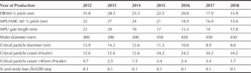
∗The data in this table have been extracted from Table FEP11—Front End Surface Preparation Technology Requirements in Ref. [1]. DRAM = dynamic random access memory; MPU = microprocessor unit; ASIC = application-specific integrated circuit; LDD = lightly doped drain.
Cleaning processes will continuously be challenged because of the further scaling down of device structures and introduction of new materials and three-dimensional device features. Removal of these “killer” particle defects must be carried out without damage to these fragile features and with essentially zero material loss (<0.1 Å) or roughening of exposed surfaces. A variety of techniques have been documented in the literature for particle removal [2]. In this chapter, dual-fluid spray cleaning is presented as it offers high potential for removal of particles from various surfaces.
2 Particles and Adhesion Forces
While filters remove particles from the gases and liquids in the wafer environment and the processing fluids, most of the particulate contamination found on wafers originates from prior processing steps, e.g. dry etch residues, chemical mechanical polishing slurries, and photoresist strip residues, or it is generated from mechanically moving parts within the processing equipment. These particulate contaminants are attached to the wafer surface by van der Waals and electrostatic double-layer forces. In addition, the condensation of water between a particle and substrate can also create a large capillary force [3,4]. A comparison of the strength of these forces is provided in Table 3.2 [3].
TABLE 3.2
Forces Acting on 100 nm Particle in Solution
| Force | Order of Magnitude (N) | Proportionality (R:Radius) |
| van der Waals | 10−7 | R |
| Electrostatic | 10−8 | – |
| Capillary | 10−8 | R |
| Drag (water, 10 m/s) | 10−9 | R |
If the particles are not removed soon after deposition, there can be a decrease in their removal efficiency in the subsequent cleaning steps [5–7]. This aging effect is believed to result from the deformation of the particle causing an increase in adhesion. It has been shown that removal of silicon dioxide (SiO2) particles under storage conditions of 40% relative humidity is more difficult than comparably sized silicon nitride (Si3N4) particles due to presumed formation of silica bridges between the SiO2 particles and silicon substrate [6]. Aging effects have higher impact on removal of smaller particles compared to larger ones [7].
3 Cleaning Process Window
The amount of force necessary to dislodge a particle must be sufficient to break the adhesion forces binding the particle to the wafer substrate but not too large to cause damage to surrounding structures. This is shown pictorially in Fig. 3.1 [8]. If the energy distribution associated with the applied force is too broad, some particles will not be removed and some damage events may occur; therefore, it is essential that cleaning processes be performed with tightly controlled energies. With the continual shrinking of device dimensions and introduction of new architectures, the strength of these features has also diminished.

FIGURE 3.1 Cleaning process window depicting particle adhesion force distribution (left) compared with structural integrity force (right) with optimized cleaning forces located in between. A color version of this figure appears in the color plate section.
3.1 Theoretical Predictions
The forces required to remove a particle have been compared to those that might damage a structure in a semiconductor device both theoretically [3,9–11] and experimentally [12–15]. The capability of different cleaning methods, e.g. standard clean 1 (SC1), megasonics, liquid jet and droplet jet, to remove particles was examined based on particle–substrate interactions [3]. After evaluating the different forces acting on particles (Table 3.2) and the potential differences between ideal spherical particles and real-world particles, the researchers selected the system of an ideal aluminum oxide (Al2O3) particle on SiO2 substrate, since this had the largest Hamaker constant (9.6 × 10⁻²⁰ J in air), and a realistic particle having a van der Waals force two orders of magnitude larger. This range of forces was deemed adequate to cover the majority of forces that might be encountered.
Theoretical performances of cleaning processes were thus examined and the results were grouped into three different types, i.e. universal processes capable of removing all particle types even from patterned wafers, processes similar to the universal group but requiring direct access to the particle, and processes incapable of removing all particles. The processes that involved fast substrate etching for particle lift-off and to enable the electrostatic repulsion to prevent particle redeposition prior to van der Waals reattachment fell into the first group. While this process has no limitation with respect to particle size, the limitations for substrate etching have changed dramatically.
Techniques that generate shock waves, e.g. droplet jet and ultrasonics/megasonics, fell into the second class of processes. The droplet jet process examined had an initial droplet velocity of 400 m/s and calculated speed upon particle impact of ∼600 m/s. As shown in Fig. 3.2, the shock wave force F, where D is the particle diameter, ρ is the density of the medium, C is the wave velocity in the medium (1500 m/s in water) and V is the speed of the medium, generated by either the droplet jet or ultrasonics techniques should be capable of removing all particle types provided there was unobstructed access to the particles.
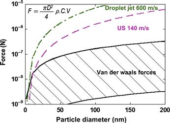
FIGURE 3.2 Droplet jet and ultrasonic (US) shock wave forces exceeding van der Waals particle attachment force.
The final group of processes, i.e. those unable to remove all particle types, included methods such as those invoking capillary forces acting on particles at the air/liquid interface of a bath and cleaning techniques using high acceleration, e.g. substrate expansion from laser exposure.
In a subsequent investigation the same researchers expanded the scope to include potential damage to structures, either deposited on the wafer surface or patterned from the substrate (bulk) [10]. In the case of the deposited structures, damage would occur when the external force applied at midheight exceeded the van der Waals force holding the structure to the substrate. The external force was linearly dependent on the line thickness. For the bulk structure, i.e. the structure patterned from the substrate, the damage criterion was selected when the stress at the base of the line exceeded 1 GPa. Calculation of this force was performed by finite element analysis using a computer software program. It was found that the maximum stress component appeared at the center of curvature at the bottom of the line. Calculations were performed for bottom radius r of 1 and 2.5 nm. The collapse forces for the bulk structures were also directly related to the line width for a given aspect ratio, albeit 20 times greater than a deposited structure.
The forces acting on particles and structures, e.g. van der Waals, capillary, drag and shock wave, during various cleaning methods were compared again to determine particle removal vs structure damage. As in the previous study, capillary forces acting on particles at the air/liquid interface of a bath were insufficient to remove all particles. However, for deposited structures with an aspect ratio greater than two, e.g. photoresist lines, it was determined that care should be taken to prevent damage. This damage potential is well known during drying of high-aspect ratio structures and the resulting issues from stiction.
The required flow velocity of 52 m/s for particle removal was found by solving the required drag force necessary to exceed the van der Waals force. While the velocity was independent of particle size, boundary layer effects were not considered. At this velocity, deposited line structures with widths <0.16 µm could be damaged but most structures were thought to be secure.
The shock wave force exerted on a particle or structure is related to the impact area; therefore, higher velocity is needed to remove smaller particles. As shown in Fig. 3.3 [10] for an aspect ratio h/e of 2, the shock wave force needed to remove critical particles can damage patterned lines, even bulk structures at ≤50 nm technology node; however, slight underetching can greatly improve the performance. The researchers concluded that a process using a high-velocity spray has to be carefully tuned in order to remove particles without damage to structures on the wafers.
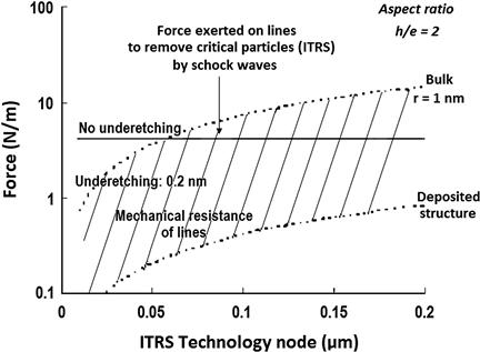
FIGURE 3.3 Comparison of the shock wave drag force necessary to remove all particles with the structural strengths of bulk and deposited structures. Reproduced by permission of ECS - The Electrochemical Society.
In a separate study, a numerical simulation using a commercial software package examined the forces involved in particle–substrate interaction in a fluid and the removal mechanism from droplet impact from a dual-fluid spray [11]. Since the dynamic contact angle was included in the operation, the evolution of the droplet impact on the surface and resulting fluid movement could be monitored to evaluate the effectiveness for particle removal. Particles in the size range of 30–100 nm were considered attached to a blanket, unpatterned substrate via van der Waals and electrostatic forces. Deionized water (DIW) was used as the cleaning fluid. Upon droplet impact on the surface, the droplet collapses and the water spreads and flows over the particles. The mechanisms for particle removal were restricted to lift and drag forces caused by the spreading hydrodynamics. Two different cases were computed, i.e. 66 and 100 µm-sized DIW droplets on a hydrophilic surface at an initial droplet velocity of 11.4 m/s.
Results showed that the removal force, whether lift or drag, was similar for both droplet sizes for particles <50 nm. If the particles were larger, the larger sized water droplet provided higher removal force. While the study could not deduce which was the fundamental force for particle removal, it concluded that dual-fluid spray cleaning should be capable of removing 30–100 nm-sized particles.
3.2 Experimental Studies
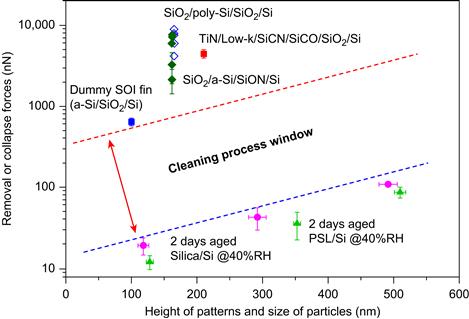
Several studies have tried to quantify experimentally the removal forces necessary to dislodge particles [12] or to damage Si-based structures [13–15] from silicon wafer surfaces to determine if a cleaning window exists for physical-based cleaning processes (Fig. 3.1). The forces were measured via lateral deflection of an atomic force microscope (AFM) tip as it contacted and dislodged or fractured the deposited particles or silicon structures, respectively, and the resulting angle from this deflection was converted into units of force. The particle removal experiments were performed by depositing either SiO2 particles or polystyrene latex (PSL) spheres in the range of 100–500 nm onto precleaned, hydrophilic silicon wafers and aging the wafers from 2 to 15 days at 0%, 40% and 100% relative humidity. Using the AFM technique, it was discovered that the silica particles became more difficult to remove as a function of increased aging time and humidity. This was attributed to formation of a water meniscus between the SiO2 particle and wafer surface since the PSL spheres showed no similar effect. The removal force for the SiO2 particles varied from ∼15 nN for the particles aged for 2 days at 0% RH up to ∼500 nN for particles aged for 15 days at 100% RH.
The forces required to damage dummy gate electrode and fin structures have likewise been quantified using the AFM technique. In one study, dummy gate structures were fabricated on the silicon substrate and consisted of layers of either (a) Si-substrate/2.4 nm SiON/100 nm amorphous-Si (a-Si)/60 nm SiO2 or (b) Si/5 nm SiO2/100 nm polycrystalline-Si (poly-Si)/60 nm SiO2 as shown in Fig. 3.4 [13]. Line widths of these gate stacks varied from 80 to 120 nm.

FIGURE 3.4 Test structures of amorphous-Si on SION (a) and polysilicon on SiO2 (b) surfaces for AFM measurements. © IOP Publishing 2013. Reproduced by permission of IOP Publishing. All rights reserved.
In a separate study [14], dummy 22 nm-wide fins were produced from a-Si deposited on SiO2 (unannealed or annealed at 1023 K), poly-Si on SiO2 or crystalline-Si (c-Si) starting from silicon-on-insulator wafers. The height of these fins varied from 60 to 80 nm and spacing between the lines was 1 µm. The same researchers later investigated dummy fins prepared from the same materials but with width of 15 nm and height of 81 nm [15]. The c-Si fins had a width of 20 nm and height of 85 nm. The a-Si fins were cut to different lengths to further investigate the effect of pattern length on collapse force.
Among the fin structures, the a-Si fins required the least force to cause damage (∼600 nN), which was attributed to a lower elastic modulus of a-Si compared to poly-Si; c-Si fins required the highest force to damage. Fins with a higher aspect ratio were also damaged more easily. The force F required ranged from 500 to 2000 nN. The collapse forces of the dummy gate stacks were larger, i.e. in the range of 2–9 µN, and varied according to the expression F = αW2, where α is the collapse coefficient and W is the line width.
The forces required to damage these structures were compared with the forces required to remove deposited particles (Fig. 3.5). As shown in Fig. 3.5, a process window theoretically still exists provided the forces utilized in the cleaning methods have a tightly controlled distribution; however, it should be noted that the apparent smaller force required to remove smaller particles compared to larger particles does not take into account boundary layer effects. As technology nodes progress and structures become even more fragile and more prone to damage, it becomes more critical to carefully control the distribution of the particle removal forces.
4 Overview of Particle Removal Techniques
The particle removal techniques can be principally divided into two separate categories, i.e. chemically or physically assisted. Since the introduction of the “RCA Standard Clean” in 1970 [16], ammonia peroxide mixtures (APM) have been used for particle removal, since the high pH (∼10) provides a net repulsion of the like-charged particles and the silicon substrate. The particle must first be liberated from the surface via underetching of the silicon substrate, which was easily accomplished with the high concentration of reagents in the original formulation. However, with the reduced substrate loss targets stipulated by the ITRS, this means of particle removal is no longer viable. The use of physical force, coupled when possible with zeta potential effects, is the only avenue currently available.
Physical removal methods most widely reported include systems like megasonics, brush scrubbing, steam-assisted laser cleaning, ice/snow aerosols, and dual-fluid sprays. Among these techniques integrated in single-wafer tools, brush scrubbing provides the highest particle removal efficiency (PRE) [17]; however, due to the forces exerted, it is primarily used for particle removal on the backside of the wafer or the unpatterned front side. Methods using ice/snow aerosols have also been reported [18], but they rely on the aerosol particles being smaller than the patterned structures on the wafer in order to remove particles located between the patterns. The earlier systems had a wide distribution of particles and velocities, which resulted in pattern damage. The technique has been further optimized to provide 10 nm-sized “bullet particles” [19,20], but the cleaning is performed in a vacuum and damage to sensitive structures is not yet known.
In batch-type wafer cleaning tools where the wafers are submerged in a tank filled with a cleaning solution, megasonics has traditionally been employed. The energy released during bubble collapse or cavitation can be adjusted through fine tuning of the appropriate frequency and regulation of the dissolved gas concentration to enable particle removal. However, with highly sensitive structures, it has become more challenging to eliminate the potential to damage the patterns. The demand for single-wafer processing tools exceeded batch tools in 2008 due to better process control, i.e. uniformity, and prevention of cross-contamination. It has been challenging to implement megasonics on a single-wafer platform due to the control that is needed in bubble size, bubble position and control over the sound field, but recent advances have been reported [21,22].
Several early reports compared the performance of megasonics with aerosol spray cleaning [23,24]. In one study, the performance of a mixed-fluid spray jet, whether on a commercial (Nanospray [25]) or experimental system, was compared against various commercial and prototype megasonic tools [23]. The cleaning solutions were either air-saturated DIW or diluted APM solutions, where oxide etch amount was maintained less than 0.5 Å. The removal efficiency of 78 nm SiO2 particles on hydrophilic 200 mm Si wafers was contrasted with damage to 70 nm poly-Si line structures.
In the case of the mixed-fluid spray cleaning, the PRE and incidence of damage both increased as a function of increased gas flow rate through the nozzle. In addition, with the commercial system, the PRE was highest and consequently more damage events were observed at positions of the wafer where the spray from the nozzle had a higher incidence rate, i.e. at wafer center and edge. The movement of the spray arm could be optimized as shown with the experimental setup to provide a more uniform spray contact time and improve the PRE across the wafer and reduce the amount of center and edge-centric damage sites. At the time this study was conducted, the performance of the mixed-fluid spray jet was superior to any of the evaluated megasonic systems; >80% PRE could be achieved without any damage to the patterned lines.
5 Dual-Fluid Spray Cleaning
5.1 System Description
Dual-fluid sprays are aerosol droplets created from the admixing of a liquid with a gas in a nozzle. The size and velocity distributions of the formed liquid droplets are dependent on the nozzle shape and dimension and the flow rates of the two fluids. Examples of spray nozzles are shown in Fig. 3.6.
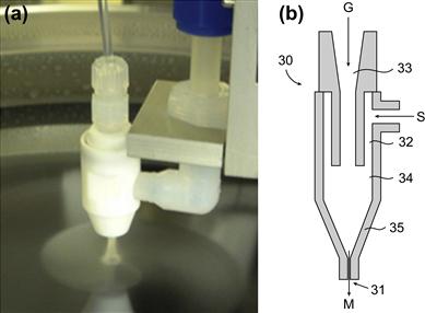
A cross-sectional view of a spray nozzle is shown in Fig. 3.6(b) [26,27]. The nozzle has a double pipe structure with the liquid being introduced through an inlet port S and gas through a separate inlet G. The two fluids are mixed in the atomizing zone 34, where a mist consisting of the fluid droplets is formed. There is an acceleration zone 35 downstream of the mixing part 34, which accelerates the formed droplet mist M from the exit orifice 31.
The formed droplets can be characterized by the Weber number We given in Eqn (3.1)
![]() (3.1)
(3.1)
where ρ is the density of the fluid, v is the velocity, d is the droplet diameter and σ is the surface tension. The formed droplet is accelerated by the gas flow and is inversely related to the droplet diameter according to 1/dα, where 1 < α < 1.5 [28].
The spray technique has been used in various industries for a variety of purposes, e.g. paint on surfaces, insecticides on plants, snow making for winter skiing, cleaning solutions for automobile car washes, to name a few. In addition, the forces of high-speed water droplets on varied surfaces, e.g. jet turbine engines, have been studied in detail to better understand how to mitigate the wear and damage to these surfaces [29].
5.2 Droplet Impact Energy
The resulting effects after a droplet impacts a surface have been widely reported in the literature. Experimental and theoretical studies have been used to better understand the mechanism and generated forces. Studies have been conducted on single droplets impacting solid, dry surfaces [30–36], malleable surfaces [37,38], droplets impacting a liquid film on solid surface [39], and droplet impact on both solid and liquid surfaces [40–42].
5.2.1 Impact on Solid Surface
During the initial stage of impact on a solid surface, the droplet is misshapen and compacted at its base. The density and compressibility of the liquid, as well as the impact velocity and droplet radius are all important parameters. After impact, the liquid in the droplet adjacent to the contacting surface is extremely compressed, but the remainder of the droplet liquid remains undisturbed.
Early studies of a single droplet impacting a rigid, inelastic surface used a one-dimensional approximation based on the water hammer theory to provide an impact pressure P given by Eqn (3.2):
![]() (3.2)
(3.2)
where P is the generated pressure, ρ0 is the liquid density, C0 is the sonic speed of the liquid, and V0 is the impact velocity. Derivation of this expression assumed that a planar shock wave moved through the liquid at a constant speed C0. While Eqn (3.2) can be used to describe the pressure created at the moment of first impact, it is insufficient to describe the maximum pressure generated. The assumptions made in the one-dimensional approach were shown by subsequent researchers to be inadequate, e.g. the velocity is not constant and the shape of the shock wave is hemispherical.
The shock wave pressure created after impact is largest at the contact edge to the substrate surface and lowest at the center. There are two different liquid zones formed in the droplet after impact, i.e. compressed and undisturbed, and they are separated by the shock wave front which propagates into the bulk liquid as shown in Fig. 3.7 [32]. The shock wave velocity may be larger than C0, but for most liquids at low impact velocities the velocities can be assumed to be equal. The generated pressure is also dependent on the target surface, i.e. a more compressible or deformable surface can absorb the energy from the droplet and weaken the resultant forces [39].
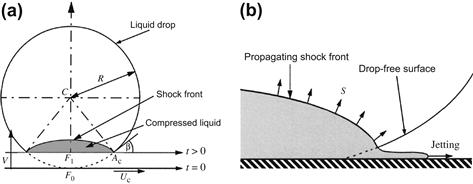
FIGURE 3.7 (a) Liquid drop impact on solid surface showing formation of a shock front. (b) Close-up view moments after impact and start of sideways liquid jetting.
A two-dimensional model was later employed to provide a better approximation of the resulting pressures up until the point of droplet spreading [30]. In this analysis, the calculated pressure at the wave front was similar to the result from the one-dimensional approach until the contact angle β in Fig. 3.7 reached half the critical angle, i.e. the radius of the shock wave when it separates from the substrate that was impacted. At this moment, the pressure increased rapidly until approximately three times the water hammer pressure in the impact velocity range of 45–450 m/s.
The hypothesis that a single shock wave is generated was shown by later researchers to result in an anomaly, which could be rectified by proposing a multiple wavelet structure [32]. In this case, the shock wave pressure at the point of contact with the substrate decreased compared to the case when only a single shock wave structure was used.
After droplet impact, the shock wave front is initially pinned to the contacting surface. After only a few nanoseconds when the contact angle exceeds a critical value does the shock wave front separate from the contact edge. At this moment, a sideways jet of liquid is formed as shown in Fig. 3.7(b). The velocity of the formed jet has been experimentally observed to be 2–5 times greater than the initial impact velocity. During this same time, an expansion wave moves into the liquid droplet, which might result in cavitation.
5.2.2 Crown Formation
The impact of a droplet on a shallow liquid layer can exhibit similar behavior as impact on a rough solid surface [43]. Both cases exhibit formation of a crown as shown in Fig. 3.8 [44] with the major difference being the longer time scale in the case of impact on a liquid film. However, if the target surface is a very smooth solid, then a crown is not formed and the liquid simply spreads across the surface. If the frequency of droplet impact is high enough, the surface of the liquid layer may not recover before the arrival of subsequent drops. If the surface is rough, this may affect the impact characteristics of succeeding drops.

Regardless of whether the impact is on a rough solid surface or a liquid film, the velocity of the base of the crown is about 10 times larger than the initial impact velocity. The height of the crown is larger in the case of impact on a liquid layer, since additional liquid is incorporated into the wall of the crown from a small cavity that is formed in the target liquid film. This cavity and crown wall will eventually collapse and form a liquid jet, referred to as a Rayleigh jet, which rises from the center of the former impacted area with the height being dependent on the impact energy.
5.2.3 Impact on Liquid Film
While the splashing characteristics may be similar between droplet impact on a liquid film vs a solid surface, the generated pressure is not. As shown in Fig. 3.9, the shock wave has to traverse the liquid layer to reach the underlying surface [45].
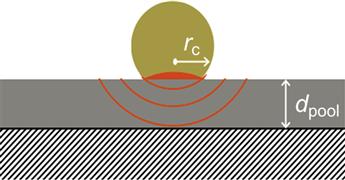
If the radius of droplet contact rc is small compared to the liquid layer thickness dpool and the thicknesses of the shock wave and liquid layer depth are both constant, the shock wave pressure generated at the substrate surface is given by Eqn (3.3).
![]() (3.3)
(3.3)
where pwh is the water hammer pressure, rc is the critical radius (∼1 µm), dpool is the depth of the liquid layer, ρ is the liquid density, s is the velocity of the droplet, v is the velocity of the shock wave, d is the diameter of the droplet and c is the speed of sound. Note that Eqn (3.3) includes an additional factor of ½ not included in the original citation, since the water hammer pressure upon impact on water is half of the value compared to the impact on a solid [46].
As shown in Eqn (3.3), the pressure upon impact now also depends on the radius of the droplet and the liquid layer thickness. The series of shock wave curves formed from droplet impact on a surface coated with a 10 µm liquid film at different velocities are shown in Fig. 3.10.
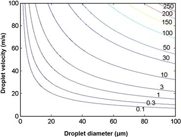
FIGURE 3.10 Pressure curves (in bar) from shock wave formed from droplet impact on a surface coated with a 10 µm liquid film at different velocities with different droplet diameters.
After the initial shock wave formation, a crown is formed and the resulting pressure Pdynamic on the surface can be estimated by Eqn (3.4).
![]() (3.4)
(3.4)
with
![]()
Note that derivation of this equation neglected any effect from the initial shock wave stage, which should be valid due to the difference in time scales of the two processes. The resulting range of dynamic pressure at the surface of a 10 µm liquid film coated surface at varying droplet sizes and diameters is shown in Fig. 3.11.

FIGURE 3.11 Dynamic pressure curves (in bar) formed from droplet impact on a surface coated with a 10 µm liquid film at different velocities and droplet diameters.
As shown, the range of dynamic pressures generated during crown formation is larger than the initial shock wave pressure. Considering the previously reported minimum velocity of 52 m/s necessary for particle removal [10], this corresponds to a minimum dynamic pressure of 13 bar in Fig. 3.11. This value is consistent with the droplet velocity values reported in the literature.
6 Dual-Fluid Spray Development
One of the first reports on utilization of the droplet impact technique for particle removal in semiconductor manufacturing was in 1998 [47]. The cleaning performance of a high-velocity water droplet spray was compared against megasonics and high-pressure water jet for removal of PSL particles from a wafer surface. The water droplets in the water droplet spray apparatus, called “M-jet scrubber” had a diameter of 10 µm and were accelerated to the wafer surface with speed varying between 50 and 330 m/s. Particles <1 µm and metal etch residues were removed without damage using the M-jet scrubber. The use of chemical solutions in the M-jet scrubber to improve the removal of small particles was also described. Additional details were subsequently disclosed [48,49].
Other researchers reported on the ability of a supersonic jet cleaning machine to remove 30 nm-sized PSL particles from a 6 inch wafer [50]. This initial report was followed by a study on the cleaning of both the front- and backside of a 200 mm wafer using droplets formed by mixing N2 gas with DIW at 3.5 kgf/cm2 (340 kPa) pressure each in a specially designed nozzle [51]. Removal of 0.3 and 0.13 µm-sized particles was compared to roll and disk-type brush scrubbing methods. While roll brush scrubbing provided better PRE, the spray cleaning was slightly better than the disk method. Particle removal was attributed by the researchers to the high impingement pressure from the twin-fluid flow spray and formed side jet of liquid.
Several years later an application of a dual-fluid spray cleaning nozzle for removal of <100 nm particles was reported [52]. The nozzle, called “Soft Spray”, dispensed ∼20 µm-sized droplets and was installed on a 200 mm single-wafer processing tool. The cleaning effect was termed “physicochemical”, i.e. the physical effect from the droplet impact and the chemical effect from the chemistries used as the liquid source. The study evaluated the effects of three different cleaning chemistries, i.e. ozonated water, diluted hydrofluoric acid and APM at three different unspecified concentrations, on wafers that were previously contaminated with either 80 nm monodisperse SiO2 or polydisperse silicon nitride (Si3N4) particles. The oxide etch rate on thermal oxide wafers was also monitored.
The cleaning sequence consisted of a first-step dispensing of hot APM solution followed by spray cleaning with the Soft Spray nozzle. In all cases, complete removal of SiO2 particles was accomplished regardless of chemistry used in the nozzle. If the Soft Spray step was not included, particle removal was negligible. For removal of nitride particles, the impact of the cleaning chemistry was more evident as shown in Fig. 3.12. Use of APM as the fluid in the spray nozzle provided an averaged removal of >98% of particles >60 nm in size. The improvement in PRE was attributed to better zeta-potential control, i.e. electrostatic repulsion between the Si3N4 particles and wafer surface. In addition, the oxide etch rate from the spray step was <1 nm/min; much less than the ∼0.14 nm/min etch rate for the hot APM step. The large variation in the data points was due to averaged results from variations in nitrogen (N2) flow rate and wafer rotation speed.
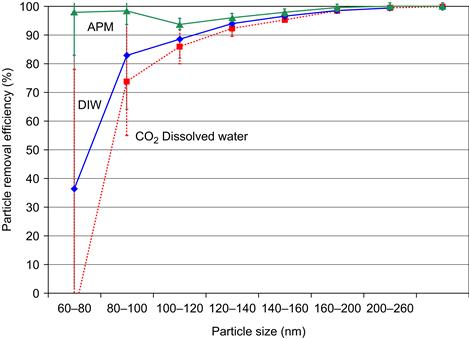
FIGURE 3.12 Averaged PRE for removal of silicon nitride particles for various fluids dispensed through Soft Spray nozzle.
After these initial publications, several papers appeared in the literature showing the benefits of dual-fluid spray cleaning for particle removal [28,53–57].
The effects from changes in the gas and liquid flows on the droplet size and velocity have been described [56,57]. Measurements of individual droplet size and velocity were performed using a Phase Doppler Particle Analysis technique. For an N2 flow rate of 25 L/min, which resulted in droplet velocity up to 63 m/s, there was a wide distribution of droplet size and velocities as shown in Fig. 3.13.
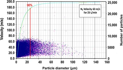
FIGURE 3.13 Droplet size and velocity distribution from atomized liquid spray with gas flow rate of 25 L/min. Reproduced by permission of ECS - The Electrochemical Society. A color version of this figure appears in the color plate section.
The arithmetic mean diameter of the 25,000 droplets ranged from 9 to 11 µm depending on the material used to fabricate the nozzle. Ninety percent of the droplets had particle diameters <25 µm. Varying the nitrogen flow rate had an inverse effect on droplet size, e.g. decrease from 30 to 20 standard liters per minute increased the average droplet diameter from 9 to 13 µm.
The effects of fluid flow rates on PRE of 0.1 µm Si3N4 particles and damage to 65 nm poly-Si lines were subsequently measured. Increasing the flow rates of DIW and N2 within the investigated flow ranges improved the PRE. If the N2 flow velocity was larger than 45 m/s, damage to the poly lines was observed. The influences of the fluid flow rates and nozzle geometry on the formed droplet size and velocity distribution were reported by several researchers subsequently.
As previously shown by Eqns (3.3) and (3.4), the resulting pressures generated upon droplet impact and crown formation are related to the droplet size. With smaller devices on wafers, droplet sizes and velocities also had to decrease to prevent damage. However, generation of a stable droplet distribution is dependent on the size and geometry of the nozzle, so continued optimization of nozzles was required to keep up with the continued introduction of advanced technology nodes.
In 2003 a new nozzle, Nanospray, was introduced that had a different design than the previous Soft Spray nozzle as depicted in Fig. 3.14. The new nozzle was constructed entirely of Teflon, was 3.5 times shorter in length and the direction in which the DIW and N2 fluid flows were introduced into the nozzle were reversed to that used in Soft Spray.
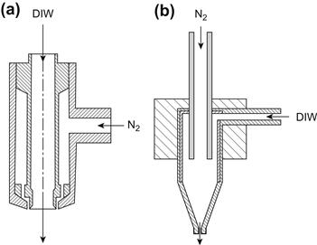
The resulting spray exiting the Nanospray nozzle was more conical in shape; the Soft Spray nozzle delivered a spray that was more columnar. The change in nozzle design provided the desired result of smaller particle diameter with a tighter size distribution. The decrease in droplet size with increase in flow velocity is shown in Fig. 3.15(a), but the change with Nanospray was not as dramatic as with Soft Spray. As shown in Fig. 3.15(b), the averaged droplet size from Nanospray decreased nearly one order of magnitude under conditions of 100 mL/min DIW and 80 L/min of N2 flows compared to Soft Spray.
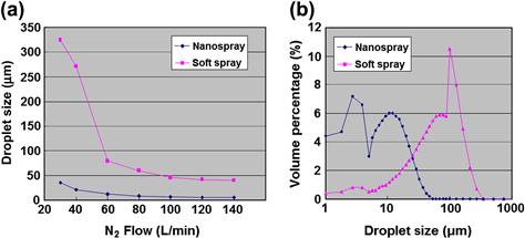
FIGURE 3.15 (a) Effect of nitrogen flow on droplet size for Soft Spray and Nanospray nozzles. (b) Droplet size distribution for Soft Spray and Nanospray nozzles at 80 L/min nitrogen flow.
Likewise >80% PRE of Si3N4 particles (>60 nm) could be achieved at an N2 flow rate of 65 L/min without damage to 70 nm poly lines as shown in Fig. 3.16.

FIGURE 3.16 Effect of N2 flow on PRE and typical damage to 70 nm poly lines using Nanospray (a). Example of typical damage to 70 nm poly line (b).
In 2006, the Nanospray nozzle was further improved to permit the cleaning of 45 nm lines without damage. To accommodate this, the nozzle was further reduced in size and the Nanospray2 nozzle was introduced to the market [58]. Similar droplet size and PRE could be achieved with Nanospray2 as with its predecessor, but at a reduced gas flow. For example, with the previous Nanospray nozzle, ∼50% PRE of Si particles >80 nm could be achieved at an N2 flow of 30 L/min; however, there were 15 instances of damage to 50 nm poly-Si lines. With Nanospray2 at half the flow rate, the PRE could be improved to 70% with no damage.
As seen in Figs 3.13 and 3.15, there was a large distribution in both the size and velocity of droplets formed by the co-mixing of liquid and gas in a nozzle. For particle removal without damage to sensitive structures as depicted in Fig. 3.1, these distributions had to be tightened to eliminate the presence of outlier droplets of large size causing structural damage. However, droplet creation via the previously described nozzle systems of mixing liquid and gaseous streams is convoluted, i.e. droplet size is inversely related to flow rate of the fluids, in particular the gas flow. A lower flow rate decreases the velocity of the formed droplets, but creates larger droplets which cause more damage. A new approach was required in nozzle design to separate the influence of fluid flow on droplet size.
7 Advanced Spray Development
7.1 Nozzle Development
A new nozzle was introduced in 2010 that enabled separate control of droplet diameter and velocity to provide optimized droplet energy [59,60]. The new, specially designed nozzle, called NanosprayÅ, uses a piezoelectric element to discharge evenly sized droplets from many discharge holes in the nozzle. This improved the cleaning efficiency and reduced the potential for pattern damage caused by variations in droplet size and velocity.
The size and velocity of each droplet were verified with a droplet measurement system consisting of a laser, high-speed camera and image processor [61].
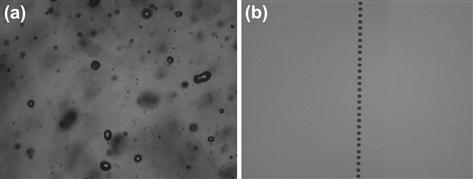
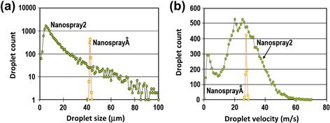
Figure 3.17 shows droplets captured by the measurement system [62]. By means of this spray nozzle, the size and velocity of droplets from NanosprayÅ are controlled in the range of ±5% (3σ). The improvement is shown visually in Fig. 3.17 and graphically in Fig. 3.18 when compared to droplets created using the Nanospray2 nozzle. In addition, the biggest advantage of the NanosprayÅ nozzle is that droplet velocity and size can be varied independently while maintaining the uniformity.
7.2 Droplet Energy Density
After verification of uniform droplet size and velocity, the effect on pattern damage was investigated [63]. A NanosprayÅ nozzle was installed on a single-wafer cleaning tool and spray processing with 22 and 40 µm-sized droplets was followed by spin drying. Three hundred millimeter wafers with photoresist structures (width = 250 nm and height = 560 nm), which were equivalent to the mechanical strength of 3× nm poly-Si gate structures, were utilized as damage test samples. As droplet velocity increased (Fig. 3.19), the amount of damage increased drastically over the starting threshold.

FIGURE 3.19 Damage to photoresist structures for two droplet sizes at varying velocity. A color version of this figure appears in the color plate section.
More damage at a lower threshold velocity was detected in the case of the larger 40 µm-sized droplets. The change in the observed linear relationship between number of damage sites with velocity was ascribed to a measurement irregularity, i.e. the measurement tool recognized damage clusters as a single damage site. Visual inspection with an optical microscope showed a large number of damage sites in the locations marked as one damage event.
The observed effect of droplet size on damage events was explained by examining the kinetic energy of the droplets on the initial impact area. Thus, the kinetic energy Ek of a droplet with diameter d moving at velocity v was calculated from Eqn (3.5).
![]() (3.5)
(3.5)
where ρ is the density of liquid. However, the kinetic energy alone was insufficient to explain the observed number of damage events. The droplet energy density Ed expresses the droplet energy within the projected area A of the droplet directly at the beginning of impact. Dividing Ek by A provided Ed as shown in Eqn (3.6).
![]() (3.6)
(3.6)
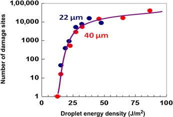
This energy Ed was used to explain the correlation of droplet energy to damage occurrence as shown in Fig. 3.20. The Ed for each droplet condition was calculated by substituting experimental values of diameter and velocity.
7.3 Damage Threshold
The concept of damage threshold energy, Eth, i.e. when the number of damage sites equals one, was likewise introduced [63]. The relationship between droplet diameter d and velocity v at this threshold condition Eth is shown in Eqn (3.7),
![]() (3.7)
(3.7)
and could be expressed as a curve separating two zones, damage-free and damage-potential zones, as shown in Fig. 3.21.
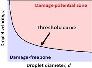
If a droplet has Ed less than Eth, it is located within the damage-free zone and has no potential for damaging structures. On the other hand, if the value is more than Eth, it is located in the zone above the threshold curve and is capable of causing damage. Of course, this threshold value varies according to the strength of the structure.
For the verification of this threshold curve, droplets dispensed from a Nanospray2 nozzle at 16 L/min N2 flow were measured and plotted as shown in Fig. 3.22. Three hundred millimeter wafers with photoresist structures (length = 250 nm and height = 560 nm) were again utilized as damage test samples. The number of droplets located in the upper damage-potential zone numbered 500 and a similar number of damages of the photoresist structures was observed experimentally. The cause of damage was ascribed to these outlier droplets, which validated the proposed concept of the threshold energy curve.
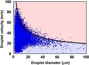
FIGURE 3.22 Damage threshold curve with Nanospray2 droplets. Below the threshold curve is a damage-free zone and above the curve is the damage-potential zone.
These relationships had been applied only to pattern damage generation, and it was not yet known if a similar relationship would be observed with particle removal. In a subsequent paper using a similar approach, the influence of droplet size and velocity for particle removal was investigated with the NanosprayÅ nozzle and contrasted with damage potential [64].
Particle removal experiments were performed on 300 mm wafers, which were previously contaminated with ∼10,000 78 nm SiO2 particles. All processes were conducted on a single-wafer cleaning tool using DIW as the fluid in a NanosprayÅ nozzle. The computer software package STAR-CD was used for simulation of the droplet impact phenomenon on a substrate. The physical strength of poly-Si gate structures of varied widths and SiO2 particle adhesion forces were measured using the AFM technique as previously described [12–15].
Figure 3.23 shows the relationship between the removed particle counts vs droplet velocity with droplet diameters of 22 µm and 40 µm. It was found that the removed particle counts increased almost linearly with the droplet velocity over the threshold with the larger droplets having a lower threshold velocity. Moreover, it was observed that the larger droplets had a higher PRE at the same velocity.
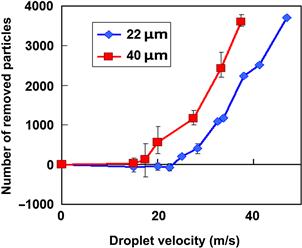
FIGURE 3.23 Relationship between droplet velocity and number of removed 78 nm SiO2 particles. Reproduced by permission of ECS - The Electrochemical Society.
The droplet energy density Ed from Eqn (3.6) was used to compare the PRE as a function of Ed as shown in Fig. 3.24. As with the pattern damage case, it was found that both droplets had the same threshold energy density Eth for particle removal. This threshold value was ∼4 J/m2, which was smaller than the pattern damage threshold value of ∼12 J/m2. From this result, it was evident that the theory of droplet energy density could explain the removal of particles, and that the particle removal and pattern damage processes were based on the same mechanism.
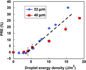
FIGURE 3.24 Relationship between droplet energy density and PRE. Reproduced by permission of ECS - The Electrochemical Society.
While the droplet energy density Ed could be used to explain the results of semiconductor wafer cleaning by dual-fluid spray droplets, the relationship between the physical phenomenon, the droplet impact pressure P and Ed was not apparent. For further understanding, the maximum pressure generated by droplet impact on a water-covered substrate was calculated at various velocities and droplet sizes. The water film thickness was held constant at 10 µm and the liquid droplet was assumed to be incompressible.
The results showed that the generated pressure depended on the droplet size d and velocity V2. The relationships were the same as the relationship of energy density shown in Eqn (3.6). Therefore, the maximum pressure at droplet impact was equivalent to droplet energy density as shown in Eqn (3.8).
![]() (3.8)
(3.8)
The threshold curves for particle removal and pattern damage generation are depicted in Fig. 3.25 along with the distributions of droplet size and velocity for Nanospray2 and NanosprayÅ. The upper curve is the threshold for pattern damage and the lower curve is the threshold for particle removal. The small grouping of points is the distribution of NanosprayÅ spray droplets, while the large distribution of triangles is the droplets from the Nanospray2 nozzle. The gap between the two curves relates to the cleaning process window for particle removal without any pattern collapse. A droplet below this gap has insufficient energy to remove particles and a droplet above this gap is capable of causing pattern damage. To improve cleaning efficiency without pattern damage, all droplets should be controlled in this gap area. The droplets from the Nanospray2 nozzle had a much wider distribution and many droplets existed outside the process window, i.e. ∼60% were located below the particle removal threshold curve and ∼3% were in the damage-potential zone. In contrast, all droplets from the NanosprayÅ nozzle were situated inside the process window. This result showed that the droplet size and velocity of the NanosprayÅ droplets could be well-controlled and this technique among dual-fluid aerosol spray methods affords the best performance for particle removal without pattern damage.
FIGURE 3.25 Threshold curves for particle removal and pattern damage generation with dual-fluid Nanospray2 and NanosprayÅ nozzles. Reproduced by permission of ECS - The Electrochemical Society. A color version of this figure appears in the color plate section.
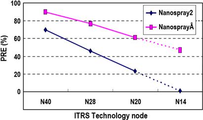
The PRE and damage threshold performances with 2× nm technology node devices were evaluated using Nanospray2 and NanosprayÅ nozzles [65]. Using spray settings that would not cause damage, the PRE performance for removal of >45 nm PSL spheres between the two nozzles is shown in Fig. 3.26. The PRE using the NanosprayÅ nozzle was 40% higher than the conventional Nanospray2 nozzle. It was estimated that with 1× nm devices, the conventional dual-fluid spray nozzle will no longer be an effective technique for damage-free particle removal.
8 Summary and Prospects
The utilization of the forces created from the droplet impact phenomena from dual-fluid spray cleaning has proven to be one of the more effective techniques for particle removal without damage in semiconductor wafer cleaning processing. Further improvement in droplet size and velocity distribution control from the development and introduction of the NanosprayÅ nozzle will extend this technique to future, more sensitive devices. However, particle removal techniques based on fluid flow are more suited for removal of large particles, i.e. smaller particles have a higher adhesion force to the wafer surface with smaller drag force experienced within the fluid boundary layer. It is expected that small particles hidden by high-aspect ratio structures will be impossible to remove with liquid motion-based processes [66].
The use of an interfacial force from freezing of water for particle removal has been reported [67]. A PRE experiment with wafers previously contaminated with different sizes of PSL particles and damage experiment with wafers patterned with 37 nm poly lines was conducted. Cold water (274 K) was dispensed onto the wafer surface and subsequently frozen by dispensing liquid nitrogen at 83 K. The formed ice was then melted by addition of 353 K hot water and the wafer dried by conventional spin drying. The PRE performance was compared to results obtained using a conventional dual-fluid spray nozzle with N2 flow of 40 L/min and DIW flow of 100 mL/min as shown in Fig. 3.27.

FIGURE 3.27 PRE results from removal of PSL spheres using conventional dual-fluid spray cleaning and frozen water.
The dual-fluid spray cleaning settings were known to be damage-free conditions for the 37 nm poly-Si line structures. The frozen water technique also exhibited no damage to the poly-Si lines and had much higher PRE performance, especially with the smallest size particle evaluated. It is expected that the introduction of this new technique will enable removal of small particles for future high technology devices.
References
1. Semiconductor Industry Association The International Technology Roadmap for Semiconductors, 2012 Update. NY: SEMATECH: Albany; 2012.
2. K. L. Mittal (Ed.), Particles on Surfaces: Detection, Adhesion and Removal.
2. (a) Particles on Surfaces: Detection, Adhesion and Removal. vol. 1. Mittal KL, ed. New York, NY: Plenum Press; 1988.
2. (b) Particles on Surfaces: Detection, Adhesion and Removal. vol. 2. Mittal KL, ed. New York, NY: Plenum Press; 1989.
2. (c) Particles on Surfaces: Detection, Adhesion and Removal. vol. 3. Mittal KL, ed. New York, NY: Plenum Press; 1991.
2. (d) Particles on Surfaces: Detection, Adhesion and Removal. vol. 4. Mittal KL, ed. New York, NY: Marcel Dekker; 1995.
2. (e) Particles on Surfaces: Detection, Adhesion and Removal. vols. 5&6. Mittal KL, ed. Utrecht, The Netherlands: VSP; 1999.
2. (f) Particles on Surfaces: Detection, Adhesion and Removal. vol. 7. Mittal KL, ed. Utrecht, The Netherlands: VSP; 2002.
2. (g) Particles on Surfaces: Detection, Adhesion and Removal. vol. 8. Mittal KL, ed. Utrecht, The Netherlands: VSP; 2003.
2. (h) Particles on Surfaces: Detection, Adhesion and Removal. vol. 9. Mittal KL, ed. Utrecht, The Netherlands: VSP; 2006.
3. Tardif F, Danel A, Raccurt O. Understanding of wet and alternative particle removal processes in microelectronics: theoretical capabilities and limitations. Warsaw, Poland: Proc. 6th IEEE Symposium on Diagnostics and Yield: Advanced Silicon Devices and Technologies for ULSI Era; 2003.
4. Bowling RA. A theoretical review of particle adhesion. In: Mittal KL, ed. New York, NY: Plenum Press; 1988;129–142. Particles on Surfaces: Detection, Adhesion and Removal. vol. 1.
5. Knotter DM, Roucou R, Peyrin R. Reduced particle removal efficiency upon wafer storage. Solid State Phenom. 2009;61:145–146.
6. Vereecke G, Veltens J, Xu K, et al. Aging phenomena in the removal of nano-particles from Si wafers. Solid State Phenom. 2008;134:155.
7. Sano K, Izumi A, Eitoku A, et al. Single wafer wet cleaning performance and particle removal >36nm. Austin, Texas: Proc. Sematech Surface Preparation and Cleaning Conference; 2006.
8. Mertens PW, Vereecke G, Vos R, et al. Roadblocks and critical aspects of cleaning for sub-65nm technologies. Hsinchu, Taiwan: Proc. 2006 International Symposium on VLSI Technology, Systems and Applications; 2006; pp. 123–126.
9. Hirano N, Takayama K, Falcovitz J, Kataoka T, Shimada K, Ando E. Microscopic analysis of particle removal by gas/liquid mixture high-speed flow. Solid State Phenom. 1999;207:65–66.
10. Tardif F, Raccurt O, Barbé JC, de Crécy F, Besson P, Danel A. Mechanical resistance of fine microstructures related to particle cleaning mechanisms. Proc. 8th International Symposium on Cleaning Technology in Semiconductor Device Manufacturing Pennington, NJ: Electrochemical Society; 2003; pp. 153–160.
11. Sun Z, Han R. Numerical studies on nano-particle removal with micro-droplet spray. Zhuhai, China: Proc. 1st IEEE International Conference on Nano/Micro Engineered and Molecular Systems; 2006; pp. 303–305.
12. Kim T, Wostyn K, Bearda T, Park JG, Mertens P, Heyns MM. Investigation of physical cleaning process window by atomic force microscope. Proc. 11th International Symposium on Cleaning and Surface Conditioning Technology in Semiconductor Device Manufacturing Pennington, NJ: Electrochemical Society; 2009; pp. 203–210.
13. Kim T-G, Wostyn K, Mertens PW, Busnaina AA, Park J-G. Collapse behavior and forces of multistack nanolines. Nanotechnol. 2010;21:1.
14. Pacco A, Kim T-G, Mertens PW. Correlation of collapse forces determined by lateral force AFM with damage generation due to physical cleaning processes. Electrochem Solid State Lett. 2011;14:H380.
15. Kim T-G, Pacco A, Wostyn K, et al. Effects of interfacial strength and dimension of structures on physical cleaning window. Solid State Phenom. 2012;195:123.
16. Kern W, Puotinen D. Cleaning solutions based on hydrogen peroxide for use in silicon semiconductor industry. RCA Rev. 1970;31:187.
17. Xu K, Vos R, Vereecke G, et al. Mechanisms of particle removal during brush scrubber cleaning. Proc. 8th International Symposium on Cleaning Technology in Semiconductor Device Manufacturing Pennington, NJ: Electrochemical Society; 2003; pp. 137–144.
18. Banerjee S, Reidy R, Rothman L. Cryogenic aerosols and supercritical fluid cleaning. In: Reinhardt K, Kern W, eds. Handbook of Silicon Wafer Cleaning Technology. second ed. Norwich, NY: William Andrew; 2008;429–478.
19. Hwang K, Lee K, Kim I, Lee J. Removal of 10-nm contaminant particles from Si wafers using argon bullet particles. J Nanoparticle Res. 2011;13:4979.
20. Kim I, Hwang K, Lee J. Removal of 10-nm contaminant particles from Si wafers using CO2 bullet particles. Nanoscale Res Lett. 2012;7:211.
21. Brems S, Pacco A, Struyf H, et al. Optimizing high frequency ultrasound cleaning in the semiconductor industry. 2012; Proc. 8th International Symposium on Cavitation, Singapore.
22. Hauptmann M, Frederickx F, Struyf H, et al. Enhancement of cavitation activity and particle removal with pulsed high frequency ultrasound and supersaturation. Ultrason Sonochem. 2013;20:69.
23. Vereecke G, Veltens T, Eitoku A, et al. Removal of nano-particles by mixed-fluid jet: evaluation of cleaning performance and comparison with megasonic. Solid State Phenom. 2008;134:193.
24. Min J, Kim N, Yang J, Park Y, Kim T. Comparison of jet spray and megasonic module for a cleaning of aluminum layer surface. Proc. 11th International Symposium on Cleaning and Surface Conditioning Technology in Semiconductor Device Manufacturing Pennington, NJ: Electrochemical Society; 2009; pp. 227–232.
25. Available from Dainippon Screen Manufacturing Co., Ltd., Kyoto, Japan. http://www.screen.co.jp/eng/index.html.
26. Nakajima K, Sato M, Sugimoto H, Hashizume A, Tsujikawa H. Substrate cleaning apparatus and substrate cleaning method. U.S. Patent 7,314,529 2008.
27. Nakajima K, Sato M, Sugimoto H, Hashizume A, Tsujikawa H. Substrate cleaning apparatus and substrate cleaning method. U.S. Patent 7,422,641 2008.
28. Fan Y, Franklin C, Abit A, et al. A Novel jet spray – meeting the challenge of damage sensitive FEOL cleaning. Austin, Texas: Proc. Sematech Surface Preparation and Cleaning Conference; 2007.
29. Bowden FP, Field JE. The brittle fracture of solids by liquid impact, by solid impact, and by shock. Proc R Soc Lond A. 1964;282:331.
30. Heymann FJ. High-speed impact between a liquid drop and a solid surface. J Appl Phys. 1969;40:5113.
31. Haller KK, Ventikos Y, Poulikakos D, Monkewitz P. Computational study of high-speed liquid droplet impact. J Appl Phys. 2002;92:2821.
32. Haller KK, Ventikos Y, Poulikakos D. Wave structure in the contact line region during high speed droplet impact on a surface: solution of the Riemann problem for the stiffened gas equation of state. J Appl Phys. 2003;93:3090.
33. Kim H-Y, Park S-Y, Min K. Imaging the high-speed impact of microdrop on solid surface. Rev Sci Instrum. 2003;74:4930.
34. Lin PA, Ortega A. The influence of surface tension and equilibrium contact angle on the spreading and receding of water droplets impacting a solid surface. Proc. 13th IEEE Thermal and Thermomechanical Phenomena in Electronic Systems (ITHERM) Conference 2012; pp. 1379–1386.
35. Chandra S, Avedisian CT. On the collision of a droplet with a solid surface. Proc R Soc Lond A. 1991;432:13.
36. Bussmann M, Chandra S, Mostaghimi J. Modeling the splash of a droplet impacting a solid surface. Phys Fluids. 2000;12:3121.
37. Haller KK, Poulikakos D, Ventikos Y, Monkewitz P. Shock wave formation in droplet impact on a rigid surface: lateral liquid motion and multiple wave structure in the contact line region. J Fluid Mech. 2003;490:1.
38. Field JE, Dear JP, Ogren JE. The effects of target compliance on liquid drop impact. J Appl Phys. 1989;65:533.
39. Sanada T, Ando K, Colonius T. Effects of target compliance on a high-speed droplet impact. Solid State Phenom. 2012;187:137.
40. Harlow FH, Shannon JP. Distortion of a splashing liquid drop. Science. 1967;157:547.
41. Harlow FH, Shannon JP. The splash of a liquid drop. J Appl Phys. 1967;38:3855.
42. Rein M. Phenomena of liquid drop impact on solid and liquid surfaces. Fluid Dyn Res. 1993;12:61.
43. Levin Z, Hobbs PV. Splashing of water drops on solid and wetted surfaces: hydrodynamics and charge separation. Philos Trans Royal Soc Lond A. 1971;269:555.
44. Randy Heisch, Untitled photo, Reprinted with permission. http://photo.net/photodb/photo?photo_id=7209027.
45. Wostyn K, Wada M, Sano K, et al. Spray systems for cleaning during semiconductor manufacturing. Lake Como, Italy: Proc. 22nd European Conference on Liquid Atomization and Spray Systems; 2008; Paper ILASS08-8-2.
46. Wostyn K. Personal Communication. 2012.
47. Kanno I, Yokoi N, Sato K. Wafer cleaning by water and gas mixture with high velocity. Proc. 5th International Symposium on Cleaning Technology in Semiconductor Device Manufacturing Pennington, NJ: Electrochemical Society; 1998; pp. 54–61.
48. Kanno I. Wafer cleaning apparatus. U.S. Patent 5,873,380 1999.
49. Kanno I, Tada M, Ogawa M. Two-fluid cleaning jet nozzle and cleaning apparatus, and method utilizing the same. U.S. Patent 5,918,817 1999.
50. Kitagawa K, Shimada K, Nishizaki K, Tatehaba Y, Yoneda T, Andou E. Removal of micro-particles by supersonic jet cleaning machine. Proc. 58th Autumn Meeting of the Japan Society of Applied Physics and Related Societies 1997; p. 842.
51. Tatehaba Y, Kitagawa K, Shimada K, Ando E. Wafer backside cleaning by twin-fluid flow cleaning. Solid State Phenom. 1999;65-66:183–186.
52. Eitoku A, Snow J, Vos R, et al. Removal of small (<100-nm) particles and metal contamination in single-wafer cleaning tool. Solid State Phenom. 2003;92:157–160.
53. Hirota Y, Kanno I, Fujiwara K, Nagayasu H, Shimose S. Damage-free wafer cleaning by water and gas mixture jet. Proc. 2005 ISSM, IEEE International Symposium on Semiconductor Manufacturing 2005; pp. 219–222.
54. Lauerhaas JM, Cleavelin R, Xiong W, Mochizuki K, Clappin B, Schulz T. Damage-free cleaning and inspection of advanced multiple-gate FETs. Solid State Technol. March 2008;48.
55. Xu K, Pichler S, Wostyn K, et al. Removal of nano-particles by aerosol spray: effect of droplet size and velocity on cleaning performance. Solid State Phenom. 2009;145–146:31.
56. Verhaverbeke S, Gouk R, Porras E, et al. An investigation of the critical parameters of an atomized, accelerated liquid spray to remove particles. ECS Trans. 2005;1:127.
57. Verhaverbeke S, Gouk R, Porras E, Ko A, Endo R. Using mixed-fluid jet bombardment for advanced particle removal. Solid State Technol. March 2006;47.
58. Dainippon Screen Manufacturing Co., Ltd., Kyoto, Japan. http://www.screen.co.jp/press/pdf/NR060705.pdf.
59. Establishment of World’s First Cleaning Technology for Ultra Miniaturization, Dainippon Screen Manufacturing Co., Ltd., Kyoto, Japan. http://www.screen.co.jp/press/pdf/NR101012E.pdf.
60. Sato M. Substrate cleaning method and substrate cleaning apparatus. U.S. Patent Application Publication US2011/0031326 2011.
61. Seike Y, Miyachi K, Shibata T, Kobayashi Y, Kurokawa S, Doi T. Silicon wafer cleaning using new liquid aerosol with controlled droplet velocity and size by rotary atomizer method. J Appl Phys. 2010;49 066701.
62. Dainippon Screen Manufacturing Co., Ltd., Kyoto, Japan, Product Photos for the Press. http://www.screen.co.jp/eng/press/nr-photo_2009-2011.html.
63. Tanaka T, Sato M, Kobayashi M, Shirakawa H. Development of a novel advanced spray technology based on investigation of droplet energy and pattern damage. Solid State Phenom. 2012;187:153.
64. Sato M, Sotoku K, Yamaguchi K, Tanaka T, Kobayashi M, Nadahara S. Analysis on threshold energy of particle removal in spray cleaning technology. Proc. 12th International Symposium on Cleaning and Surface Conditioning Technology in Semiconductor Device Manufacturing Pennington, NJ: Electrochemical Society; 2011; pp. 75–82.
65. Chien Y-HC, Yeh M, Ku S, et al. Physical cleaning enhancement using advanced spray with uniform droplet control. Solid State Phenom. 2013;195:195.
66. Brems S, Hauptmann M. Process window – boundary layer effects. Unpublished Report, IMEC, Leuven, Belgium 2012.
67. Snow J, Nadahara S. Advanced particle removal techniques for <20nm device node. Austin, TX: Proc. Sematech Surface Preparation and Cleaning Conference; 2012.