3
The Backscattering Technique and its Application
Before starting …
Today backscattering and shunt regulator techniques in RFID are not new … but their mutual incidences are not very well known. So, to give to the reader a good and complete overview about this complex subject, a significant part of the content of this chapter is issued from the already existing Dominique Paret books: RFID en Ultra et Super Hautes Fréquences UHF-SHF: Théorie et mise en oeuvre, Dunod, 2005/2008, and the English version RFID at Ultra and Super High Frequencies: Theory and Application, John Wiley, 2009.
As shown in previous chapters, the power Ps reflected or reradiated by the tag (which is dependent on the value of the power flux density s) can be received and detected by the receiving antenna of the base station and can thus act as a signal informing the base station of whether or not an object or tag is present in the electromagnetic field.
Also, while the tag is illuminated, and regardless of whether it is remotely powered or locally battery assisted, provided that it has been designed to respond accurately via a specific modulation, it is called “backscattering modulation”, which will be described in detail later on.
Therefore, it is useful to analyze the way in which the radar cross section (RCS) is varied or modulated, and to define the extent of its variation – the quantity Δσe s – as a function of a possible coding and a specific modulation, which will enable us to determine its ability to be understood correctly by the base station. We will then proceed to determine what its merit factor is, or ought to be.
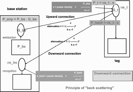
3.1. Backscattering principle of communication by between-base station and tag
As a general rule, allowing for exceptions (and there are some), the communication model followed by standard RFID systems used at UHF and SHF is based on the reader talk first (RTF) principle, using half-duplex mode (an alternating link between the base station and the tag).
The stages of transmission are summarized in Figure 3.1.
3.1.1. The forward link: communication from the base station to the tag
During the first phase, known as the forward link of the half-duplex, the base station transmits the carrier frequency to remotely power the batteryless tag. During this phase, the carrier frequency is modulated (in amplitude shift keying (ASK) mode, for example) for the transmission of the command and interrogation codes to the tag.
Figure 3.1. Principle of backscattering: forward link
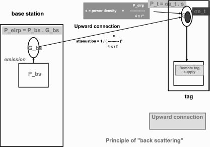
Note that, during this phase, the tag illuminated by the incident electromagnetic wave may either absorb the power that it receives or reradiate some of it, depending on the state of its antenna/load impedance matching. Generally, for remotely powered tags, the tag is made to absorb the maximum possible power (i.e. with no standing waves) during this phase, in order to provide the best possible remote power supply and thus achieve the highest possible operating distance. However, it may reradiate during this phase, according to its “structural” aspect.
To sum up, during the forward link we have:
3.1.2. The return link: communication from the tag to the base station
During the second phase of the half-duplex, called the “return link”, with transmission from the tag, the base station initially supplies or maintains the sustained pure (unmodulated) carrier frequency to provide a physical support for the tag’s response following the preceding interrogation commands. During this return link phase, two operating subphases may be present, depending on the binary information to be transmitted by the tag to the base station:
a) Either the transmission of no useful information or the transmission of a logical “1”: note that these are often identical in physical terms, since they correspond to the same phenomenon as that described in the previous section concerning the forward link.
b) Alternatively, the transmission of a logical “0”: in this case, the tag’s electronic circuit modulates the value of the load impedance Zl = Rl + Xl of the tag antenna at the rate of an on-off keying (OOK) modulation corresponding to the logical data to be transmitted. Thus, at the tag, there will be an impedance mismatch between the source (the tag antenna) and its load, leading to the appearance of standing waves, and therefore to a new effective RCS and a variation of the RCS area, which will immediately modify the amount of power reradiated in a different way from that described in the previous section.
NOTES.–
The receiving part of the base station examines the content of the return path (the return link) during subphases (a) and (b) only (Figure 3.2.).
To make this phenomenon easier to understand, the explanations above relate to the case of simple bit coding (NRZ) of the return link. This bit coding is often different (Manchester, BPSK, FM0, etc.).
To sum up, during the return link we have:
Figure 3.2. Principle of backscattering a) return link, tag matched/tuned; b) “modulation“ return link
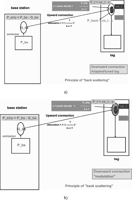
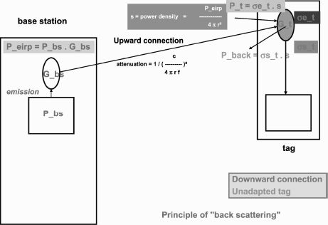
Figure 3.3. Principle of backscattering: return link, tag mismatched
The communication concept of the return link as outlined above is the main basis of UHF and SHF RFID systems operating in a mode of detecting the value of the reradiated/scattered return wave, known as the backscattering modulation mode.
Figure 3.4. Principle of backscattering: return link
Let us now examine the details of the phenomena produced by the tag in the return link, during the return wave modulation phase, for example the transmission of a logical “0” from the tag, starting from the optimal matching conditions mentioned above. Let us see what happens when we change the load impedance to values outside the optimal matching conditions mentioned above.
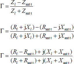
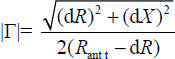
As indicated previously, the deliberate modulation of the load impedance Zl leads to an impedance mismatch between the source and the charge, on one hand, and the presence of a wave reradiation phenomenon, on the other hand. Therefore, we can examine this problem of impedance modification in terms of a “distributed constant line” and quantify this mismatch by using the reflection factor to calculate it.
3.2. The merit factor of a tag, Δσe s or ΔRCS
As shown above, in RFID applications, which operate on the backscattering principle and which are therefore based on the principle of modulating the wave reradiated by the tag, the effective RCS of the tag σe s varies when the impedance of the tag antenna is deliberately modified by changing the value of its resistive and/or capacitive part.
3.2.1. Definition of the variation of the radar cross section, σe s or ΔRCS
The resulting variation of σe s or RCS leads to the appearance of a new parameter, called Δ σe s or ΔRCS = σe s modulated – σe s unmodulated due to the modulation of the antenna impedance, which represents the difference between the two corresponding “unmodulated” and “modulated” values of σe s.
![]()
NOTES.–
1) In the technical literature, Δσe s or ΔRCS is also called the “merit figure” or “merit factor” of an RFID tag.
2) Theoretically, the merit factor Δσe s should be defined not as a scalar magnitude but as a vector value (i.e. complex variable) and therefore it includes amplitude and direction (or modulus and phase), allowing for all the complex impedances involved.
This is because, depending on the different modulation states (particularly in the case of BPSK or QPSK), the values of the reradiated scattered power in watts may be equal while the phases of the scattered waves are different, and the difference of the scalar quantities Δσe s between two states of modulation may be zero. To avoid this, the demodulator in the receiving part of the base station must allow for this possibility and must therefore be capable of demodulating either the amplitude or the phase of the received signal equally well.
Let us now take an overview of its variations as a function of the different parameters.
3.2.2. Estimation of Δσe s as a function of ΔΓ
In an RFID application, we do not know in advance what the initial “unmodulated” position of the tag corresponds to in physical terms (is it matched, nearly matched or completely unmatched?), or what the corresponding value of Γ1 = Γnon modulated will be. To make matters clear, the “unmodulated” physical state depends on the principles adopted for the design of the application. For example, the system designer may decide that the tag should be of the battery assisted type (having an incorporated battery, but still of the passive communication type return link) because the application requires operation at very long range, in which case the tag antenna does not necessarily have to be matched in advance in the “unmodulated” position to recover the maximum energy, since a battery is provided in the tag.
By contrast with many currently available books on this subject, I will cover every possible kind of application by stating, without any prior assumptions, that
Γ1= Γnonmodulated (initial value in the unmodulated position)
Γ2 = Γmodulated (the value when the load impedance is switched, i.e. in the modulated position)
![]()
Using the general equation, we can write:
Because the structure of the equation σe s = σe s structural + σe s antenna mode has a fixed part and a variable part, the difference between the “modulated” and “unmodulated” states is simply the algebraic difference between the two values of the variable part of the equation σe s antenna mode, namely σe s antenna mode mod and σe s antenna mode non mod (Figure 3.5).
![]()
Now let us calculate the corresponding values of σe s1 and σe s2. We obtain:
After reduction, the merit factor becomes:
Finally, by replacing Γ2 in this equation by its value (Δ Γ + Γ1), we obtain:
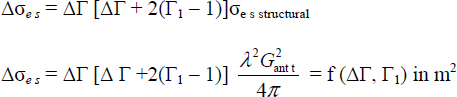
Figure 3.5. Calculation and variations of Δσe s = ΔRCS
It is very important to note that the function Δσe s = ΔRCS is simultaneously dependent on two elements: the variable ΔΓ and a parameter representing the initial value of Γ1.
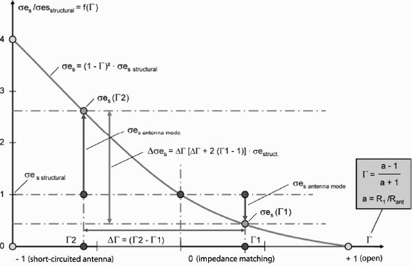
3.2.3. The variation Δσe s = f(ΔΓ,Γ1)
Let us return to the general equation for Δσe s found above:
![]()
First, we should note that the value of Δσe s is a function of two intercorrelated variables, and for simplicity we will examine the case where Δσe s = f(ΔΓ) with Γ1 = constant.
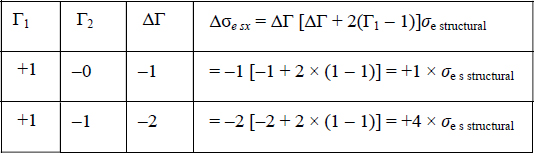
Let us start with an observation. Theoretically, the maximum variation of ΔΓ is limited to the range of 0–2 inclusive, because the value of Γ can vary from –1 to +1. In practice, in the case of numerous RFID applications of the remotely powered type, this range of variation will be smaller (from 0 to – 1) because of the need to recover some of the incident energy to supply the remotely powered tags (see the list in Table 3.1).
Now let us take a closer look at the two very common cases shown in the first two columns in Table 3.1, which represent the great majority of conventional RFID applications.
Large number of RFID applications operate in “remotely powered” mode and therefore start from the initial unmodulated position with conjugate matching, i.e. Rl = Rant t and a = 1, in other words, Γ1 = 0, and then switches to a value of Rl different from that of Rant t, giving rise to a new value, Γ2. In this case alone, ΔΓ = Γ2, and the above equation is simplified and reduced to the form:

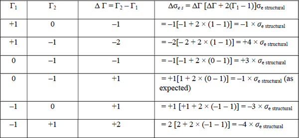
Table 3.2 shows examples of values of Δσe s.

Let us look at two subcases that frequently arise when Γ1 = 0.
– Subcase 1
Rl is often switched all the way from the conjugate matching condition, Rl = Rant t, a = 1, to Rl = 0 (load short-circuited) in UHF RFID, in order to maximize the variation of the value of Δσe s. This simultaneously gives rise to two conditions, a = 0 and Γ = –1, and therefore:
![]()
– Subcase 2
In RFID, it is sometimes desirable to reach a compromise between the variation of the RCS and the power consumption of the tag in order to optimize the operating range of the system, and therefore Rl is made to change only very slightly about the matching value Rant t. In this case only, a = Rl/Rant t, i.e. close to or substantially equal to 1, and that Γ2 is (very) close to 0 (matching). In this case, Γ22 will be small with respect to –2Γ2. Consequently, in this particular case only,
![]()
which fits very well on the curve (the slope of the curve where a = 1, i.e. Γ = 0).
If there is no need to provide a remote power supply to the tag, because the applications concerned use battery-assisted tags, then our aim will clearly be to benefit from the wider variation of Δσe s by switching the load condition from “fully open” to completely “short-circuited”. If the initial value of Γ in the unmodulated condition, Γ1, is equal to 1 (i.e. there is an open load) – and only in this case – the above equation becomes:
![]()
and clearly we can write
![]()
an equation which appears in many books and documents in this field … but unfortunately with no indication of the limits of its validity (battery-assisted tags only). So we should be careful with unforeseen results. Table 3.3 shows the values for Γ1 = 1.
An example in RFID (remotely powered tag)
In general and specific terms, in order to modulate the area Δσe s of the tag, the value of Rl is reduced by what is known as “load modulation”, or else we modify the value of the tuning capacitance upward or downward, using a variable capacitance diode; very often, it is not possible to modify both of these simultaneously, as the resistive part of the load Rl = Rant t takes a value of (Rant t – dR) and its reactive part Xl = –Xant t takes a value of (–Xant t + dX). Let us return to the original general equation for the current I flowing through the equivalent circuit:
![]()
and multiply the numerator and denominator by the conjugated quantity of the denominator:

Then it becomes:
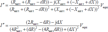
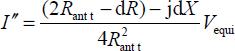
Hypothetical cases of tag operation
Let us assume that the total load impedance is only slightly different from that of the matching condition, in other words, dR is small with respect to Rant t, and/or dX is small with respect to Xant t, and therefore the terms (dR)2, (dX)2 and (4Rant t dR) of the equation above are negligible with respect to the others.
Thus, we obtain:
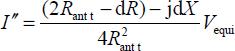
and therefore, finally:

Now let us calculate the new effective RCS σ″e s during this phase of impedance modulation. We can do this by using the same type of calculation as before.
We know that, by definition, the new power reradiated by the tag P″s is equal to:
![]()
Since we know the new complex value of I″:
we can calculate its effective value (in other words, the value of its modulus):

and then square it:
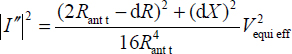
In this case (transponder impedance modulation), the reradiated power P″s will, therefore, be:
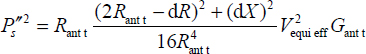
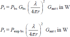
We also know that the total structural power Pt received by the tag from the base station is:
![]()
and therefore
and the reradiated power P″s will now be:
![]()
and therefore:
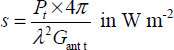
![]()
Now we can transfer the value of s into the equation for σe s, then replace P″s with its value, which gives us:
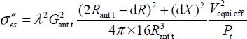
We have seen that, when the impedances of the tag antenna and the load are matched, the power Pt is equal to the power dissipated in the load, i.e.:

If we include this value into the preceding equation, we obtain:

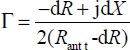
If we expand the numerator, provided that dR is assumed to be small, in other words that dR2 and dX2 are negligible because they are of the second order with respect to the other terms of the equation, we find:

In conclusion, given the structure of the resulting equation, we can identify (1 – dR /Rant t) with (1 – Γ)2 = (1 – 2Γ + Γ2) ~ (1 – 2Γ) because dR ![]() Rant t, and therefore the value of Γ2 is much smaller than that of Γ, and so:
Rant t, and therefore the value of Γ2 is much smaller than that of Γ, and so:

We could have expected this because
and if Rl is close to Rant t (and therefore dR is small), a is close to 1:

A few notes
I may have spent a long time in setting out and presenting all the foregoing equations, only achieving useful approximations at the end of a series of proofs, but this has not been done in a spirit of excessive masochism. I have acted in this way purely because I wanted to allow readers and users to provide their own simplifications in the course of their calculations, in line with the specific circumstances of their RFID applications.
I should also point out that this equation does not depend on dX, and therefore, in this case, the variation of the RCS is essentially due to the load variation dR, and the phase does not change to any great extent.
Another note
I could have followed a direct argument based on Γ.
If we now multiply the numerator and denominator of this expression by the conjugate of the denominator, we obtain:

If there is optimal matching, (the output impedance of the antenna and the input impedance of the integrated circuit are conjugate, i.e. Rl, = Rant t and Xl, = –Xant t), then Γ = 0 and the maximum available power will be transferred to the load. Before going more deeply into the theory, let us return to the specifics of UHF and SHF RFID applications. The tag impedance will be matched and then slightly mismatched; in other words, the resistive part of the load Rl, = Rant t will take the value of (Rant t – dR) and its reactive part Xl = –Xant t will move to a value of (–Xant t + dX).
By replacing Rl and Xl with their new values in the equation for Γ, with no simplification, we obtain:

Assuming that the variations of resistance dR and reactance dX are small (a small detuning of the tag), in a first approximation we can disregard the terms dR2, dX2 and the product (dRdX), which are all of the second order. After simplification, we have:
and since dR ![]() Rant t:
Rant t:

Given that, when the tag is only very slightly mismatched,
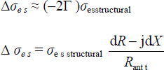
The value in brackets is the tag modulation merit factor and shows the real and imaginary parts that may be included in the value of Δσe s.
Important note about UHF RFID systems using backscattering phase modulation
It should be noted that, based on the assumptions stated at the start of these explanations, if the value of dR is very small or even zero, and if only the value of dX is significantly modified (for example by modifying or modulating only the internal capacitance of the integrated circuit of the tag, or, in other words, by keeping Zant equal to Zl in the forward link from the base station to the tag), the value of Δσe s is a purely imaginary quantity. Essentially, this means that there is no change in the reradiated power in watts (backscattering) between the forward and return link phases of communication, and that only the phase of the signal reradiated by the tag is modified by the (reactive) impedance modulation of the integrated circuit. In this case, the base station receiver has to carry out a phase demodulation of the backscattering signal, instead of performing amplitude variation demodulation of the ASK type on the received power as before. By way of information, 99% of commercially available base stations, which for many other reasons have I, Q demodulators, always carry out simultaneous amplitude and phase modulation.
Matching factor
To conclude this example, let us now calculate the value of the matching factor (actually the mismatching factor) of the tag:
![]()
To do this, we start by calculating the modulus of this expression:
and then square it:

NOTE.–
Theoretically, the input impedance Rl of the integrated circuit is not equal to 73 Ω. Consequently, there is always an impedance matching circuit (a transformer or an LC circuit) which adjusts the impedance represented by the integrated circuit (about 35 μW at 2 V with P = U2/Rl → Rlic = 80 kΩ) to 73 Ω.
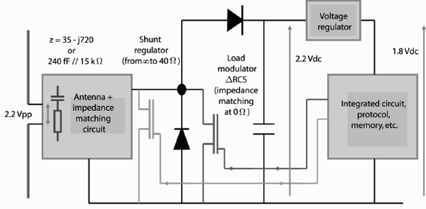
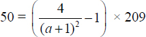
3.3. Variations of Δσe s = f(a)
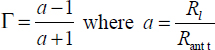
For reasons of simplicity, we often prefer to consider the variations of Δσe s not as a function of Γ, but as a function of a = Rl/Rant. We can do this by returning to the previous general equation, Δσe s = f(Γ) and replacing Γ with its value as a function of a. Given that:
![]()
we can now calculate Δσe s = (Δσe s – σe s structural), for the case of optimal matching:

Now we are “theoretically” ready to apply the backscattering principle to RFID technology but first of all we had better confront the cold hard facts, if only for a few moments.
3.4. After the theory, RFID at UHF and SHF realities
We have now concluded our study of the theory of σe s/RCS and other forms of Δσe s and ΔRCS, which is absolutely necessary, but not sufficient. Everything we have said about the variations of σes/RCS relates to the best possible world, in which the tag can effortlessly handle very small fields E and H (when the tag is at a long distance from the base station) and very large fields E and H (when the tag is located very near the base station).
In fact, if the tag is going to be able to operate correctly at both long and short distances, we must include a new element in the integrated circuit, namely a “shunt regulator”, to ensure that excessive voltages do not appear across its terminals in the presence of strong fields.
Everything discussed so far relates to the phase of operation when this regulator is inactive, which is important, since it defines the maximum operating distance of the system. As the tag approaches the base station, the shunt regulator increasingly comes into action in parallel at the input of the integrated circuit, thus mismatching the load from the radiation resistance of the antenna Rant, causing a displacement of the reference point (where there is no modulation) which, therefore, approaches the vertical axis of the curve, making the value of ΔRCS smaller than before. This makes it harder to guarantee the variation ΔRCS for operation in proximity.
Figure 3.6. UHF tag: block diagram (whole circuit)
It is worth examining these matters in detail for remotely powered tags (used in most applications, therefore mainly with Γ1 = 0), as this will help us understand the phenomena occurring in RFID at UHF and SHF. In order to do this, we need to examine the true equivalent electrical circuit of the tag, while also considering the effects of its distance from the base station.
Tag located very far from the base station
In this case, the tag does not receive (does not capture) enough energy to be remotely powered, so nothing happens, and the problem is solved.
Tag exactly on its operating threshold (maximum distance)
The tag begins to receive the exactly correct minimum amount (threshold) of power. The shunt regulator does not come into action (Rshunt is infinite), meaning that the tag benefits from all the possible incident energy supplied by the wave from the base station (Figure 3.7)
The “load modulation transistor” comes into action as required when data need to be sent from the tag to the base station, and switches the load impedance of the tag antenna and moves, in the case of a remotely powered tag, from the “matched” value (anon mod = Rl/Rant t = 1) (in order to obtain the maximum power) to the value amod = (Rmatch in parallel with Rmod)/Rant t), enabling the initial backscattering area σstructural to be modified to a higher value (σe s/RCS) in order to reradiate more of the incident wave. The graphs in Figure 3.8 summarize the variation of ΔRCS in the case of very weak fields.
Figure 3.7. Tag in the thresholdfield

Figure 3.8. Graph showing the variation of ΔRCS in the case of very weak fields
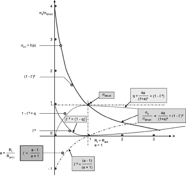
The resistance Rmod must be chosen in such a way that it allows the base station to understand and interpret the data (in the form of power variations) transmitted by the tag, and therefore the value of ΔRCS shown in the diagram must be above a minimum level. Consequently, there is a maximum ohmic value of Rmod max, and therefore of amod and Γmod. An example of a calculation is given below for UHF applications according to ISO 18000-6 (UHF) and 18000-4 (2.45GHz), in other words with ΔRCSmin of 50 cm2 (see the example below).
Of course, we could consider making life simpler by having Rmod equal to 0 Ω, thus immediately providing (see Figure 3.9) the greatest possible variation of the area ΔRCS, provided that this has no effect on the energy consumed by the tag – but that is another story.
Figure 3.9. Optimizing the variation of the load resistance for the highest value of ΔRCS
Example: Δσe s and conformity with ISO 18000-6 in the threshold field
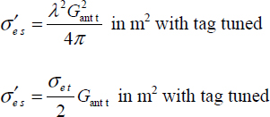
To ensure high compatibility of tags and base stations, the “Tag Parameter: 7d” of ISO 18000-6 states that “the tag ΔRCS (Varying Radar Cross Sectional area) affects system performance. A typical value is greater than 0.005 m2 = 50 cm2.” This means that, regardless of the frequency within the 860–960 MHz band (the mandatory range for conformity with ISO 18000-6), the minimum typical value of Δσe s is 50 cm2. Additionally, given that the value of σe s structural is 0.214 λ2 for a λ/2 dipole tag antenna with a gain of 1.64, and that
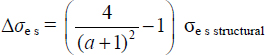
we can estimate the minimum value of a = Rl/Rant t to satisfy the equation Δσe s =50 cm2.
a) If the frequency = 960 MHz, λ = 0.3125 m and σe s structural = 209 cm2:
and therefore a = 0.797;
b) If the frequency = 860 MHz, λ = 349 m and σe s structural = 260 cm2:

and therefore a = 0.83
where Rant t = 73.128 Ω and Rl = aRant t, with these conditions we can find the maximum value of the minimum value of Rl.
In case (a): Rlmin = 58.28 Ω and therefore Γmin = –0.113.
In case (b): Rlmin = 60.7 Ω and therefore Γmin = –0.093.
NOTE.–
With these very low values of Γmin (about –0.1), we are in the area where Γ can be expected to approach zero; thus:
![]()
and therefore
![]()
Tag entering its normal operating range
The tag is now correctly supplied with power, even above its strict minimum level. The shunt regulator comes into action (or comes back into action) to limit the voltage at the input of the integrated circuit (Figure 3.10).
Figure 3.10. Tag in the medium field – the shunt regulator starts to conduct normally

For this purpose, the value of Rshunt decreases (by a few kilo-ohms) and is connected directly in parallel with the load resistance of the antenna, thus causing a structural mismatch of the antenna, even if there is no modulation by the modulation transistor, and a decrease of the nominal value (without modulation) of a which thus becomes a′ = (Rl in parallel with Rshunt)/Rant t. This is equivalent the displacement of the initial operating point of a =1, Γ1 = 0 (the point corresponding to the operating threshold) toward a′ < 1 and Γ1 other than zero and with a slightly negative value (Figure 3.11).
According to the data to be transmitted to the base station, the modulation transistor of the tag comes into operation and switches the above value (a′) (which is no longer the matched value, so the maximum power is no longer received, although this does not upset the tag because it is closer to the base station) to the value Rmod, thus modifying the backscattering area (RCS) in order to reradiate more of the incident wave.
Figure 3.11. Variations of the position of Γ1 as a function of the field strength
As shown in the diagram, this modulation changes the value of a, but also causes a further variation of ΔRCS, which is smaller than the previous variation. Furthermore, the value of ΔRCS decreases as the tag approaches the base station. The question which then arises is: will we fall below the minimum ΔRCS required by the standard? To answer this question, we must consider the most unfavorable limiting case, which is present when…
The tag is located extremely close to the base station
The tag is correctly powered, even well above its absolute minimum level (Figure 3.12).
Figure 3.12. Tag in a strong field – the shunt regulator is fully conducting
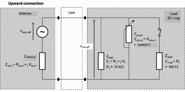
The shunt regulator is in full operation, thus limiting the voltage at the input of the integrated circuit. For this purpose, the value of Rshunt becomes very low (at a few ohms to a few tens of ohms) and is connected directly in parallel with the load resistance of the antenna, thus causing a very large structural mismatch of the antenna, even if there is no modulation by the modulation transistor, and therefore a very large decrease of the nominal value (without modulation) of a which thus becomes a″ = (Rl in parallel with Rshunt)/Rant t. This is equivalent to shifting the initial operating point (at the operating threshold) of a = 1 toward a″ which is located very close to the vertical axis in Figure 3.13, and bringing Γ1 close to the value of –1.
According to the data to be transmitted to the base station, the modulation transistor continues to attempt to operate, switching the value a″ to the value (Radapt//Rshunt //Rmod ![]() Rshunt //Rmod) to modify the backscattering area (RCS) as much as possible in order to reradiate some of the incident waves.
Rshunt //Rmod) to modify the backscattering area (RCS) as much as possible in order to reradiate some of the incident waves.
As shown in the diagram, this modulation not only changes the overall value of a and Γ, but also causes a further variation of ΔRCS, which is even smaller than the previous variation. Being very close to the vertical axis, the value of ΔRCS is even smaller, but must be greater than the minimum value of ΔRCS required by the standard. This limits both the minimum range and the value of Rshunt, and therefore the maximum strength of the field E that the tag can accept. Also, for simple reasons of power dissipation, chip manufacturers specify a maximum input current for their integrated circuits, for example 10 or 30 mA eff (refer to the first two chapters of this book, if necessary, for more information).
Figure 3.13. The limiting case of the position of Γ1 in a strong field
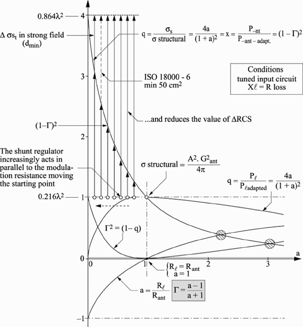
Example of a real case and conformity with ISO 18000-6 in strong fields
As we have just seen, as the tag approaches the base station the shunt regulator comes increasingly into operation, and the value of Γ1 (in the phase without modulation of the antenna load) tends toward –1.
If we wish to comply with ISO 18000-6, even in strong fields, the value of Δσe s typical must be equal to 50 cm2. Using a λ/2 dipole in which the value of σe structural is approximately 200 cm2 at 900 MHz, and short-circuiting the antenna entirely in the modulation phase, our aim is to obtain Γ2 = –1 during the modulation. We can use the equations shown above to determine the critical value of Γ1 corresponding to this condition:

Transferring the values:
![]()
we obtain a second degree equation in Γ1, [–Γ21 + 2Γ1 + 2.75], whose roots are
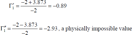
that is Γ1 = –0.89 (tag unmodulated, in a strong field, with shunt fully operational).
We can now determine the value of a as follows:

which shows that, in order not to exceed the minimum value required by ISO 180006, the minimum value of the shunt resistance must not fall below Rshunt min = 0.058 × 73 = 4.24 Ω (with Rant t of 73 Ω on matching). The position of this point is shown in Figure 3.13 above.
By way of conclusion
As shown above, the value of Δσe s decreases as we approach the base station. Precise measurements show that the measured variation of Δσe s is substantially proportional to r2. Additionally, the variation of the power reradiated by the tag, ΔP, is equal to sΔσe s. Now, the incident power flux density s is equal to ![]() , indicating that the ΔP reradiated by the tag is substantially constant regardless of the distance at which it operates; this property being mainly due to the presence and operation of the shunt regulator.
, indicating that the ΔP reradiated by the tag is substantially constant regardless of the distance at which it operates; this property being mainly due to the presence and operation of the shunt regulator.
This concludes the major theoretical part of this section of the chapter which is primarily concerned with reflection, absorption and the backscattering transmission principles and their effects. Unfortunately, as you will certainly have realized, the concepts of RCS and Δσe s (or ΔRCS) are rather difficult to grasp, and the values involved are not very easy to measure.
3.5. Measuring ΔRCS
As I have shown above, when the tag circuit modulates the value of RCS, this is done by using a transistor operating in switch mode, in other words on an “on/off” basis, and therefore using square wave signals (with or without subcarriers) which, when antenna mismatching takes place, produce a frequency spectrum including sidebands that are located on either side of the carrier frequency and that thus represent the modulating signal.
Most of the energy of the signal reradiated by the tag and representing the transmitted data is therefore in these sidebands, and this is also the location of the power present in the return signal, since, if we keep strictly to the conceptual aspect of the RCS (measurement of the return power contained in the incident carrier only) we may find it very difficult to recover the signal. Also, we can use return modulation of the Manchester subcarrier coding (SCM) or BPSK type, as for RFID operating at 13.56 MHz (ISO 14443 and 15693), in an attempt to escape from the use of the unwieldy carrier signal for the amplification and demodulation of the very weak return signal.
3.5.1. Example of a method for measuring ΔRCS
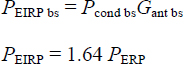
Returning to our topic, we can obtain the value of Δσe s (often called ΔRCS) by using the measurement setup shown in Figure 3.14, in which a base station supplies/transmits a constant isotropic power PbEIRP = PcondGant bs. The power flux density radiated by the base station and present at the tag, at a distance r1 from the base station, is, as expected,
![]()
Figure 3.14. Method of measuring ΔRCS

Let Ps tag EIRP denote the (difference in) global power EIRP reradiated by the tag when the return wave is modulated by modulation of the tag impedance using a square wave signal with a peak amplitude h. This is analyzed in a conventional way into the Fourier series:

indicating that the amplitude of the first harmonic (the fundamental frequency) of the function that produces it is greater than 4/π (=1.27) at the initial value h of the square wave signal. Also, assuming that this square wave signal creates an amplitude modulation (AM) of the incident UHF/SHF carrier, the two reradiated sidebands created by this modulation support the signal.
Given that:
we can write:
a) Umax = Uc + 2 Uh
b) Umin = Uc – 2 Uh
and Umin = 0, when we perform 100% AM (ASK).
If we now simplify matters by identifying the real square wave signal Uh with its first harmonic and call the amplitude of its first harmonic (fundamental) Us,1, Fourier analysis gives us:
![]()
and if we transfer this value into the above equations, we obtain:
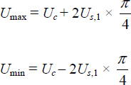
Since Umin is equal to 0 in AM of the 100% ASK type, we can combine the last two equations to give:
![]()
This voltage-based description can be rephrased in terms of power (proportionally to the square of the voltage). This entails a relationship such that the power reradiated by the tag (and therefore received by any receiver) Pmax corresponding to Umax is equal to:
![]()
where Ps,1 is the power contained in the first sideband reradiated by the tag, which is about 10 times greater than that expected from a purely static (or slow) modulation of the tag impedance, provided that the return signal is only read by a detector whose analysis aperture has a narrow bandwidth (a few kHz) to ensure that only the sideband(s) due to the modulation signal are observed. Figure 3.15 provides an idea of the spectrum reradiated by the tag as a result of modulation by a conventional square wave signal.
Figure 3.15. Example of a spectrum of the reradiated power

If we only consider the reradiated power Ps,1 contained in the first harmonic of the spectrum, this will act as an equivalent isotropic transmission source for the backscattering signal, Ps,1 tag EIRP, part of which, Precept, is recovered (in the first harmonic of the spectrum) at the receiver with a gain of Gant recept located at a distance r2, according to the Friis equation:
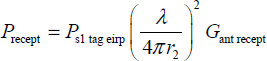
and therefore:
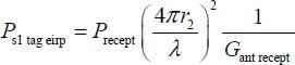
By definition, the variation of the RCS of the tag, ΔRCS, representing the ratio between retransmitted power and the incident power flux density will be:

Combining the last of the above equations, we finally obtain:

Pcond is the conducted power of the base station and Gant bs is the gain of the base station transmitting antenna:
![]()
where r1 is the distance between the tag and the transmitting antenna of the base station, r2 is the distance between the tag and the antenna of the measuring receiver, Gant recept is the gain of the receiving antenna of the measuring receiver, Precept is the power received and measured in the first sideband of the spectrum and λ is the wavelength of the carrier wave.
By applying this last formula to the measured value Precept, we can find the value of Δσe s which can be used in practice.
Note that all of these proposed measurement methods have been accepted as the basis for the measurement of ΔRCS in ISO 18047-6 entitled “Conformance Tests” for RFID at UHF.
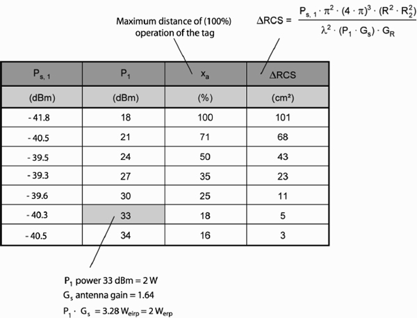
By way of information, an example of values of Δσe s (measured and then calculated) as a function of the power contained in the first harmonic of the switched signal is shown in Figure 3.16.
As shown above, the value of Δσe s becomes increasingly difficult to determine as we approach the base station. “Up to what point?” the reader may well ask. Figure 3.17 shows a few “bad examples”.
Note that there are two remarkable facts about this diagram:
Figure 3.16. Example of measured and calculated values of Δσe s
To finish with this subject, one should always remember that, as mentioned above, because of the necessary presence of a regulator in the tag to enable it to operate correctly in weak (far) fields and strong (very near) fields, the return modulation index will also depend on the distance, and therefore it is not as simple as it may appear to ensure a minimum value of ΔRCS.
Developers of UHF and SHF base stations have therefore familiarized themselves with all the methods of signal amplification, selection and processing, and, if this is not your main area of expertise, I suggest that you consult the many specialist books about HF signals – or, if all else fails, contact the authors.
Figure 3.17. Examples of measured values of Δσe s in commercial tags

3.6. The “Radar” equation
Finally, let us now consider the radar equation.
Power reradiated by the tag and power received by the base station
Remember that, as a general rule,
![]()
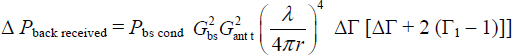
whose value depends on both the variation of ΔΓ and the initial point of this variation Γ1; therefore, when the load impedance of the tag antenna circuit is modulated, the difference in power reradiated by the tag, ΔPback, between the “non-modulation” and “modulation” phases will be:

and the difference in power received at the base station (allowing for the gain of its antenna) will be:
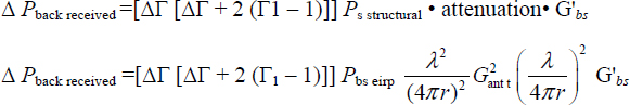
Given that Pbs EIRP = Pbs cond G′bs:
This general equation enables us to design the receiving stages of the base station to make them capable of receiving and detecting the small fraction of power ΔPback which is reradiated by the tag via the variation of the area ΔRCS (see the example in the preceding chapter).
3.7. Appendix: summary of the principal formulas
Antenna gain
For an isotropic dipole: gain = 1.5 or in dB = 10 log(1.5) = 1.76 dB.
For an isotropic λ/2 dipole: gain = 1.64 or in dB = 10 log(1.64) = 2.14 dB.
Power
Power flux density produced by the base station

Effective area of the tag
![]()
Power received by the tag
![]()
The Friis equation
Attenuation coefficient (in air)

attenuation (in dB)= –147.56 + 20 log f + 20 log r where f is in Hz and d is in m.
Power reflected by the tag
![]()
Effective area or radar cross section
Power reflected/scattered/reradiated by the transponder

Power flux density reradiated by the tag

Return power received by the base station (three ways of writing the same equation)

Merit factor of the tag