
2
Design of UHF RFID Tags
2.1. Tag antenna design
Radio frequency identification (RFID) tag antennas present unique design challenges to satisfy heavy constraints due to cost and size. The antenna miniaturization on inexpensive materials is only one of several problems that a designer needs to solve, others being the wideband impedance matching to the RFID integrated circuit (IC) and the sensitivity to the environment. Section 2.1.1 describes the fundamental circuit parameters of the dipole antenna. As most ultra high frequency (UHF) RFID tags are dipole-based structures, dipole issues regarding the input impedance, radiation resistance, efficiency, quality factor (Q-factor) and impedance will be of practical interest in the design of tag antennas. For polarization, radiation pattern and propagation issues, readers can refer to [BAL 05] and [DOB 12]. Then, miniaturization strategies based on fat dipoles, tip loading and meanders are presented in sections 2.1.2 and 2.1.3. The last section (section 2.1.4) addresses the influence of the dielectric and metallic environments on the tag performance.
2.1.1. Fundamental circuit parameters of the dipole antenna
2.1.1.1. Equivalent electrical circuit
The dipole forms the basis of most tag antenna designs. It can be built with either metallic wires or strips. Considering the dipole in Figure 2.1, when a potential is applied to the antenna inputs, there is opposite charge buildup on the ends. Essentially, the dipole ends can be viewed as open circuits, with a high voltage and no current. Due to the charge buildup at either end of the dipole, current begins to flow. Therefore, any antenna simultaneously stores charge and opposes changes in current. These phenomena are, respectively, associated with a capacitor and an inductor in an electrical model. If the distance between positive and negative sources is comparable with a wavelength, the retardation in going from different parts of the dipole to a point in space prevents radiation cancellation and produces reinforcement of effects in a certain direction. This energy flow into the environment can be modeled by a resistance.
Figure 2.1. Charge and current distributions in a dipole antenna. Near-field distributions of the E- and H-components

Ignoring the influence of the antenna thickness, the length of a UHF band half-wave dipole antenna is about 16.4 cm at 915 MHz. Over a relatively narrow bandwidth (5%) near resonance, the half-wave dipole resonance can be fairly well predicted by a series RLC circuit (Figure 2.2). The reactance tends to follow the series LC circuit but the resistance is not constant in reality. The resonant frequency of such a circuit is given by:
[2.1] ![]()
Figure 2.2. Equivalent series RLC circuit of a half-wave dipole antenna
The basic half-wave dipole is not the appropriate solution in UHF RFID for two reasons. First, its length is too long for UHF labels. Second, the antenna reactance at resonance is too low and its resistance is too high to match the typically low equivalent series resistance and high capacitance of UHF RFID ICs.
Antennas in the RFID industry often have a length of approximately 92 mm because of the convenience of placing tags within a 102.6 mm wide label. But a straight dipole shorter than a half-wave has a negative reactance. Therefore, an additional inductance must be synthesized to make the short antenna resonate at a lower frequency than its natural resonant frequency. At this stage, it is useful to introduce the following relationships [MCD 12] for the total capacitance C and inductance L of a short wire dipole of length l and diameter b:
[2.2] 
[2.3] ![]()
These equations are valid for l![]() c/f0 = λ0. For l = 3.33 cm, i.e. l = λ0/10
c/f0 = λ0. For l = 3.33 cm, i.e. l = λ0/10![]() λ0 at 900 MHz, we would find C = 0.26 pF and L = 11.6 nH with b = 1 mm. It is easy to show that the reactance Lω-1/Cω of a short linear antenna is largely due to its capacitance. By replacing the rough estimates of L and C in [2.1], we obtain l = λ0/2.22, which gives a fairly good prediction of “resonance” and physical modeling even for a half-wave dipole.
λ0 at 900 MHz, we would find C = 0.26 pF and L = 11.6 nH with b = 1 mm. It is easy to show that the reactance Lω-1/Cω of a short linear antenna is largely due to its capacitance. By replacing the rough estimates of L and C in [2.1], we obtain l = λ0/2.22, which gives a fairly good prediction of “resonance” and physical modeling even for a half-wave dipole.
2.1.1.2. Radiation resistance, input impedance, efficiency and gain
The radiation resistance Rrad of an antenna is defined as the resistance that would dissipate the same amount of power as the antenna radiates, when the current in this resistance is equal to the current maximum in the antenna. On the other hand, the input impedance Za of any antenna is defined as the ratio of the voltage and the current at its terminals. For a center-fed dipole, the maximum current and the current at the terminals only coincide if 1≤λ0 (Figure 2.3). Under these conditions, we can state that the input resistance equals the radiation resistance (Ra = Re(Za) = Rrad) for a lossless dipole.
The input impedance Zas of a dipole with an offset feeding (asymmetric) can be related to the input impedance Zs of a center-fed (symmetric) dipole of the same length. The impedances Zas and Zs relate to the radiated power through their respective current magnitudes at the dipole terminals Ias and Is (Figure 2.4). Imposing the condition that, for a given current distribution, the power delivered by the transmitter must be equal to the sum of the radiated (active) and stored (reactive) power of the antenna leads to
[2.4] ![]()
The offset feeding of the asymmetric dipole is located at a distance h from the dipole center. Assuming a sinusoidal current distribution, [2.4] becomes:
[2.5] 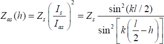
which further reduces to the following expression for a half-wave dipole:
[2.6] ![]()
Figure 2.3. Current distribution along the dipole antenna for various antenna lengths
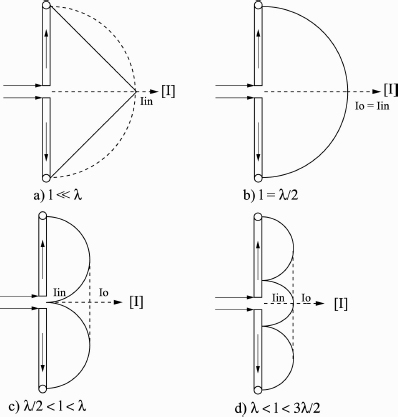
Figure 2.4. Illustration of the relation between the input impedances for the asymmetric and symmetric dipole feeds

We conclude that both the input resistance and reactance can be increased by offsetting the antenna input toward the dipole ends where the current goes to 0. It is important to note that the radiation resistance is identical for all positions but it is only in the center-fed case that the real part of the input impedance equates the radiation resistance.
In a lossy antenna, the input resistance Ra can be separated into a series circuit of two different resistors:
[2.7] ![]()
where Rrad is the radiation resistance and Rloss is the loss resistance representing the unwanted losses caused by the non-perfect conductors and dielectric materials. The radiation resistance of a wire or strip dipole strongly depends on the current distribution. For the “ideal” (1![]() λ) dipole, the current is uniform and the radiation resistance is given by [BAL 05]:
λ) dipole, the current is uniform and the radiation resistance is given by [BAL 05]:
[2.8] 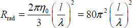
It can be shown that for a small dipole (λ/50<1≤λ/10), the current is triangular, maximum at the center and zero at the ends (Figure 2.3). Then, a good approximation is of one-fourth of [2.8]:
[2.9] 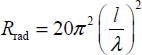
For longer dipoles, the current is distributed as a sine wave. The radiation resistance of a center-fed dipole can be approximated with a high degree of accuracy [TAI 07] as:
[2.10] ![]()
for a frequency range verifying f0/20 < f < 1.2f0. Therefore, [2.10] is valid for dipole lengths around a half-wave, the upper limit being l = 0.6λ0.
It can be noted that all previous Rrad expressions do not depend on the antenna diameter, which is correct as long as l/b is very large. As a result, Rrad decreases slightly when the dipole is made thicker. For b/λ = 0.003 corresponding to b = 1mm at 900 MHz, Rrad ~ 62 Ω whereas the ideal value when b→0 should be 73 Ω. Although the radius of the wire does not strongly influence the resistances, the gap spacing at the feed plays a significant role, especially when the current at and near the feed point is small.
Finally, the loss resistance due to conductive losses can be calculated with:
[2.11] 
The antenna efficiency η is defined as the ratio:
[2.12] 
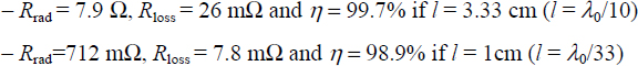
which is the ratio of the radiated power and the input power of the antenna. Assuming a working frequency of 900 MHz (λ0 = 33 cm) and a dipole in free space (no substrate losses), a straight dipole of conductivity σ = 5.7 × 10⁷ S/m (copper) with b = 1mm will be characterized by:
To have a better control over the antenna resistance, a loading bar with the same width as the meander trace is added in [RAO 05]. Working as a shunt capacitance, it helps to trim the radiation resistance to the IC input resistance (Figure 2.5).
Figure 2.5. Meandered dipole with a loading bar for radiation resistance trimming
The term “antenna gain” describes how much power is transmitted in the direction of peak radiation to that of an isotropic source. Let us assume that an antenna is made up of with conductive materials of zero resistivity and that the dielectrics present no losses. Calling Glossless the gain of this ideal lossless antenna, the peak gain G of the same antenna made up of lossy material is given by:
[2.13] ![]()
where η is the efficiency of the lossy antenna. Since antenna gain affects both the efficiency of the power transfer to the chip and the portion of the incident power that will be reflected back to the reader, it is very important to maximize the generally low, due to size, antenna gain.
2.1.1.3. VSWR bandwidth and Q-factor
The antenna bandwidth (BW) can be defined from any of its fundamental characteristics such as the return loss, input impedance, polarization and radiation efficiency. In order to relate the antenna bandwidth to the Q-factor, it is more convenient to use the matched voltage-standing-wave-ratio (VSWR) bandwidth BWVSWR. For an antenna tuned, i.e. showing a zero reactance, at a frequency ω0, BWVSWR is the difference Δω between the two frequencies on either side of ω0 at which VSWR equals a constant S. The fractional matched VSWR bandwidth is then defined as:
[2.14] ![]()
This definition is only valid if the characteristic impedance of the feedline equals Za(ω0)=Ra(ω0). The half-power VSWR bandwidth corresponds to S = 5.828. The associated value of the magnitude squared of the reflection coefficient is α = (S-1)2/(S +1)2 = 1/2, which means that one half of the incident power is reflected back.
In the context of resonators, the Q-factor is 2π times the ratio of the energy stored in the resonator (sum of energies stored in lossless inductors and capacitors) to the lost energy per cycle dissipated in resistors at the resonant frequency:
[2.15] 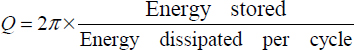
The concept of the Q-factor is used to describe the antenna as a resonator. Usually, in circuit design we want elements to have a high Q-factor in order to reduce the circuit loss. However, when talking about antennas we want a low Q-factor because the “loss” involved is the radiation we really want. A low-Q antenna shows a wider bandwidth as:
[2.16] ![]()
Conversely, a large-Q antenna is characterized by a sharp resonance and a narrow bandwidth because it stores a lot of energy and radiates relatively little of it.
The concept of the Q-factor is very useful when considering small antennas. The Q-value of the small antenna is high due to the low radiation resistance and the high reactance. The smaller the antenna, the higher the Q-value expected. Hence, the bandwidth of a small antenna is inherently narrow. But the Q-factor can be improved, i.e. reduced for a given antenna volume if appropriate design strategies are applied [BES 05]. A reliable relationship between FBWVSWR and Q has been established in [YAG 05]:
[2.17] 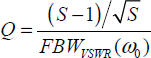
Figure 2.6 shows the Q-factor as a function of the wire radius a = b/2 normalized to the wavelength for a half-wave dipole. It can be observed that the Q-factor is roughly Q = 4.4 for a 1.65 mm radius, i.e. 100 × a/λ = 0.5. However, according to [STU 12, Figure 6.7, pp. 159], FBWVSWR is 16% for S = 2 and 100 × a/λ = 0.5. By replacing these two values in [2.17], we obtain Q = 4.41, which is in close agreement with the graphic value.
The worldwide frequency range of UHF RFID tags is defined between 860 and 960 MHz over an 11% fractional bandwidth. We conclude that there is no problem in covering the 11% UHF RFID world band with a straight half-wave dipole. But size reduction techniques described in the next sections (meanders and capacitive loading) increase the Q-factor up to 15, which makes the Q improvement a primary performance issue. Obviously, efforts on the Q-factor could be minimized if the tags are dedicated to a single band, for instance United States (US) only.
An additional drawback of narrowband antennas is that they are more difficult to match and more susceptible to detuning than wideband antennas.
Figure 2.6. Q factor as a function of dipole radius a=b/2 [HAZ 11]

From Figure 2.6, it is also clear that Q decreases logarithmically with (a/λ). As a result, dividing Q by only 2, for instance from 6 to 3, requires a wire diameter 15 times thicker (from 0.6 mm to 10 mm). So, large variations of the aspect ratio length/diameter result in a weak Q improvement.
[MCL 96] has described the fundamental theoretical limit for the minimum Q-value of a small antenna. If the antenna can be placed inside a bounding sphere of radius r, the minimum Q-value for a lossless antenna is
[2.18] 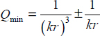
where k = 2π/λ. This expresses the absolute minimum Q value the antenna can take. Unfortunately, the theory does not tell us how to implement a minimum Q antenna. However, a key point is that an antenna that fills the volume efficiently will be able to reduce the total reactive fields, resulting in a lower Q. Best [BES 05] has shown that an antenna made up of multiple folded arms in the spherical helix geometry occupies the full spherical volume, achieves self-resonance and an impedance match. The optimal result is within 1.5 times the theoretical lower bound on Q for an electric dipole showing an efficiency of 98%.
But RFID antennas are planar and a dipole only fills a small part of the volume of the bounding sphere. Consequently, the optimal Q-factor which is roughly equal to 1 for a sphere of radius r = λ/2 using [2.18] is also much lower than the Q values extracted from Figure 2.6.
Up to this point, we have only considered wire dipoles. It useful to admit that the bandwidth of a flat dipole with width w is roughly equivalent to the bandwidth of a wire dipole with diameter b if w = 2b [DEA 10].
2.1.2. Fat antennas and tip loading
As shown in [2.1], at a given resonance frequency, the product of L and C will result in a certain fixed value. Although the product is fixed, the relation of L/C can be chosen arbitrarily. As an example, doubling C and halving L will result in the same resonance frequency. This gives some freedom in the design of the dipole, which means that it is possible to design various kinds of dipoles with different shapes, which all have the same resonance frequency. The difference between two dipoles with the same resonant frequency but a different L/C-ratio is the Q-factor and hence the bandwidth, since
[2.19] 
Clearly, the L/C-ratio has to be minimized in order to obtain a high bandwidth of the dipole. Using the expressions [2.2] and [2.3] for L and C valid for short dipoles, we found that:
[2.20] ![]()
where l and b are the length and diameter of the wire, respectively. We conclude that increasing the dipole diameter favors the Q-factor in two ways: increasing the wire thickness reduces its self-inductance and increasing the conducting surface results in a larger capacitance. [2.10] explains the logarithm dependence of the Q-curve in Figure 2.6.
Broadband fat tags may also increase manufacturing cost, depending on the techniques used for antenna definition. Etching based on subtractive processes makes more sense than expensive silver ink printing if the purpose is to keep maximum of metal. Nevertheless, fat tag antennas have seen wide commercial deployment. Some typical broadband structures are given in Figure 2.7. Manufacturers advise us to use fat tags for high dielectric mounting glass, wood and plastic or challenging metal/plastic/fluid containers.
Figure 2.7. Examples of Alien fat tags with broadband features

On the other hand, Q is also improved if R is made larger. Obviously, the antenna Q can be reduced by introducing loss in addition to the radiation resistance, but this would reduce the antenna efficiency. We have seen in section 2.1.1.2 that the radiation resistance is basically a function of the wire length. Therefore, increasing l would be a solution but the size reduction is mandatory. The question is: how can we increase Rrad with a reduced antenna length? The answer is in the current dependence of Rrad. Assuming a dipole length l = 100 mm (i.e. λ/3 at 900 MHz), [2.9] gives Rrad = 21.9 Ω for a triangular distribution of the current and [2.10] gives Rrad = 24.5 Ω for a sine distribution. As Rrad is four times greater for a uniform current than a triangular one, we would expect 4 × 21.9 Ω = 87.6 Ω if a uniform distribution of current could be enforced along the wire.
The following question is how can we make the current distribution as uniform as possible when l and λ are of the same order? The idea is:
There are basically two practical ways to achieve that:
Figure 2.8. Size reduction by loading the dipole ends with packed meanders

Figure 2.9. Tip-loading: principle of dipole miniaturization with uniform current [DOB 12]

Figure 2.10. EPC Gen 2 RFID inlays with tip-loadings: a) Alien ALN-9662, b) Texas instruments and c) Alien 9634

We conclude that capacitive loading has the advantage of physically shortening the element length at the end of the dipole where the current is lowest (least radiation), and without introducing noticeable losses as inductors do. End-loaded short dipoles have the highest radiation resistance, and the intrinsic losses of the loading device are negligible.
2.1.3. Meandered dipoles
In this section, it is shown that a half-wave dipole of length l can be made shorter by folding the wire back and forth and creating meanders (Figure 2.11). For the same resonant frequency as the original half-wave dipole, the resulting meandered dipole antenna (MDA) is characterized by a “mechanical” length s shorter than l in the original horizontal direction without considering the vertical segments. However, the “physical length” stot>l represents the total wire length of the MDA accounting both for the vertical and horizontal segments. Conversely, the resonant frequency can be decreased by loading a meander line structure onto a half-wave dipole for a fixed antenna length.
Wire-based MDAs can be found in few use cases. For instance, inox cylindrical wires are used in RFID labels implemented in linens and clothes to support the harsh washing process of industrial laundries. But nearly all RFID antennas are some variants of printed MDAs. Currently, copper is the most commonly used conductor in tag antennas and etching is the most widely used manufacturing technique to produce the conductive patterns. However, the tag cost is a crucial factor in the mass production of antennas. Economical manufacturing methods can be achieved by applying printing techniques using conductive ink. In printed electronics, silver particles are often used to form the conductive layer of the metal-line on the tag antenna.
Figure 2.11. Typical geometry of a meander dipole and a half-wave dipole (s<l and stot>l)

The main outcome of this section is that the resonant frequency declines as some features increase such as the meander height h, the number of folds m, the meander width w and the conducting line length s. Moreover, the loaded position of the meanders does not affect the resonant frequency but strongly modifies the gain performance.
2.1.3.1. Analytical analysis of the structure
The analysis of the structure can be made as follows [END 00]. The influence of the meander part of the antenna is similar to a load, and the meander line sections are considered as shorted-terminated transmission lines. Figure 2.12 shows a dipole antenna with two meanders. Each meander is treated as a twin line with a short-circuited termination. In addition, the bold line and the dashed line are considered as a straight conducting line with length s and diameter b.
Figure 2.12. Meander line sections seen as shorted-terminated transmission lines
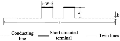
The characteristic impedance of twin lines can be expressed in the following form:
where η is the wave impedance in free space, w is the distance between twin lines and b is the diameter of the conducting line. Zin is the input impedance of twin lines, given by the following equation:
[2.22] 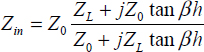
where β is equal to 2π/λ and h is the height of the twin lines. Assuming that all twin lines are terminated in a short circuit, the load impedance of the twin lines is zero (ZL=0) and [2.22] becomes:
[2.23] ![]()
where tanβh can be expanded into three orders on condition that βh![]() 1.
1.
[2.24] ![]()
Then a new expression of input impedance is obtained:
[2.25] 
If we insert [2.21] into [2.25], the reactance formed by each twin line can be shown to be:
[2.26] 
where μ0 is the vacuum permeability. On the assumption that the number of meanders is m, the total reactance obtained by the twin lines should be Lp = m×L. The straight conducting line, whose length is s, also results in a self-inductance. It is given by the following equation [END 00]:
[2.27] 
The total inductive reactance of the MDA is finally given by:
[2.28] ![]()
The self-inductance of a half-wavelength dipole antenna can also be derived from [2.27]:
[2.29] 
Following [END 00], we suppose that the inductive reactances of the MDA and the half-wave dipole antenna are the same when they resonate at the same frequency. Thus, LH = LT at f0 = c/λ0 leading to:
[2.30] 
[2.30] states the relationship between the resonant frequency f0 of the MDA and its physical dimensions.
2.1.3.2. Influence of the meander characteristics on the resonant frequency
MDAs loaded with different numbers of meanders are selected as shown in Figure 2.13, where the number of meanders m = 2, 8 or 14, the length of MDA s = 129 mm, the wire diameter b = 1 mm and the gap between dipole arms g = 3 mm [HU 09].
Figure 2.13. Topology of the three MDAs under study

In order to establish the influence brought by each parameter on the resonant frequency, the following methodology is used. Two of the three values (m, h, w) are fixed while the unfixed one is changed over a range. To examine the validity of the analytical model, the simulation software Ansoft high frequency structural simulator (HFSS) is used for comparison.
The number of meanders m is changed from 2 to 14 (w = 6 mm, h = 10 mm). The resonant frequency calculated by [2.30] and HFSS is derived, as shown in Figure 2.14. Similarly, the variation of resonant frequency caused by the meander height and width is shown in Figures 2.15 and 2.16 for m = 2, 8 and 14. It is observed that the original size of the half-wave dipole can be reduced by nearly 50% with 14 meanders.
Figure 2.14. Resonant frequency as a function of the number of meanders (w = 6 mm, h = 10 mm)

The influence of the positions of the meanders can be studied by moving them toward the end of the dipole (distance D in Figure 2.13) with unchanged meander dimensions (w = 6 mm, h = 10 mm). The resonant properties analyzed by [2.30] and HFSS are illustrated in Figure 2.17. We note that D does not have a strong effect on the resonant frequency. Overall, the resonant characteristics of the MDA predicted by [2.30] are in general agreement with simulation results and are getting closer with the increase of the number of meanders.
Figure 2.15. Resonant frequency as a function of the meander height (w = 6 mm)
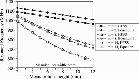
Figure 2.16. Resonant frequency as a function of the meander width (h = 10 mm)
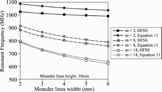
Figure 2.17. Resonant frequency as a function of the position D of the meanders

2.1.3.3. Discussion on the MDA reactance
The inductance of twin wires is lower than the inductance of a wire of the same length. For instance, assuming a diameter b = 1 mm, a straight wire of length l = 100 mm yields L = 100 nH with [2.27], whereas we find 60 nH for twin wires of height h = 47.5 mm and width w = 5 mm with [2.26]. Therefore, the inductance of a straight dipole will be always higher than that of an MDA if the length of the straight dipole and the total “physical” length of the MDA wire are identical. A densely packed meandered antenna has significantly less inductance per unit length than a straight dipole.
However, the total capacitance of an MDA is also reduced compared to a straight dipole. This can be deduced from the rough approximation [2.2] of the capacitance for short dipoles. Since the resonant frequency of an antenna is equal to ![]() where L and C are the inductance and capacitance of the antenna, respectively, we conclude that a longer “physical” length stot is required for an MDA that would have been the case using a straight dipole to obtain the same 900 MHz operation.
where L and C are the inductance and capacitance of the antenna, respectively, we conclude that a longer “physical” length stot is required for an MDA that would have been the case using a straight dipole to obtain the same 900 MHz operation.
2.1.3.4. Influence of the meander characteristics on the gain and the radiation resistance
A standard half-wave dipole antenna is modeled in HFSS. Its length l = 129 mm is the same as that of the MDA discussed in the previous section. A comparison is made between the gain of the half-wave dipole and that of the MDA with a fixed “mechanical” length s = 129 mm. The gains are all derived at the half-wave dipole resonant frequency 1.095 GHz and the MDA resonant frequencies. The comparison is shown in Tables 2.1 and 2.2. It is demonstrated that the MDA gain decreases as the number of meanders, their height and width increase.
Table 2.1. MDA gain for different numbers of meanders and meander heights (w=6 mm)

Table 2.2. MDA gain for different numbers of meanders and meander widths (h=10 mm)

The gain drop with MDAs can be explained as follows. The currents on the two parallel vertical wires which compose the twin lines are flowing in opposite directions. Consequently, these currents do not radiate but contribute to the magnetic near-field and the conducting losses. In other words, a meander increases not only the antenna inductance but also its loss resistance Rloss. On the other hand, the uncompensated currents in the horizontal segments of the meanders contribute to the radiation. As the total lengths of horizontal currents in the MDA and the half-wave dipole are both equal to 129 mm, it can be assumed that both antennas have the same radiation resistance Rrad. Therefore, the antenna efficiency given by η = Rrad/(Rrad + Rloss) is reduced with the MDA and meanders lower the antenna efficiency and gain. In conclusion, increasing the number of meanders does not improve the radiation ability but actually results in more losses, i.e. compromise should be made between the size reduction and the gain.
Another important point is that the position of the meanders along the MDAs has some impact on the gain. As the current along a resonant dipole is minimum at its ends and maximum at its center, it is preferable to concentrate the meanders at the ends rather than in the center to reduce the losses, whereas the total inductance is independent of the meanders’ position.
Conversely, if the MDA is squeezed to keep the same resonant frequency as the half-wave dipole then the radiation resistance Rrad, meander of the MDA can be deduced from the radiation resistance of the half-wave dipole Rrad, half-wave by [DOB 12]:
[2.31] 
2.1.4. Influence of dielectric and metallic materials – losses and detuning
This section focuses on the influence of the materials used in the fabrication of antenna tags, i.e. the conducting metal-line and the dielectric substrate. The losses due to these parameters and the impact on the antenna efficiency are first studied. Then, the detuning effect on the resonant frequency and the input impedance will be analyzed.
2.1.4.1. General formulation of the dielectric and conducting losses
It is reminded that the power dissipation in dielectric heating in a dielectric volume (V) is given by:
[2.32] ![]()
where εr and tanδ are the relative permittivity and the loss tangent of the dielectric, respectively. As dielectric losses increase in proportion to tanδ, we conclude that the larger the value of the loss tangent, the more energy is converted from electric field into heat. This means that if there is a lossy dielectric material near a tag, the tag will lose some received power from the reader in the dielectric and we would expect to see a reduction in the tag antenna performance. Materials having polar molecules, such as water, especially tend to have high dielectric losses. However, the challenge in having good tag performance in the presence of targets containing water is not only due to the high dielectric losses, but also due to the high relative permittivity value of water, which is approximately 81.
The power dissipation due to ohmic conduction over a metallic surface (S) is given by:
[2.33] ![]()
where ![]() is the component of the magnetic field tangent to the surface and Rs is the surface resistance given by:
is the component of the magnetic field tangent to the surface and Rs is the surface resistance given by:
[2.34] ![]()
We conclude that conducting losses increase in proportion to ![]() . In a good conductor at high frequencies, such as UHF, current density is packed into the regions near the conductor surface. The depth below the surface of a conductor at which the amplitude of an incident electric field has decreased by a factor 1/e is called the skin depth
. In a good conductor at high frequencies, such as UHF, current density is packed into the regions near the conductor surface. The depth below the surface of a conductor at which the amplitude of an incident electric field has decreased by a factor 1/e is called the skin depth ![]() . The δ-value is roughly 2 μm for copper at 900 MHz. When the conductor thickness is equal or less than the skin depth, the superficial resistance becomes inversely proportional to the conductor thickness. Therefore, a printed RFID antenna whose thickness is smaller than the skin depth will have a low efficiency.
. The δ-value is roughly 2 μm for copper at 900 MHz. When the conductor thickness is equal or less than the skin depth, the superficial resistance becomes inversely proportional to the conductor thickness. Therefore, a printed RFID antenna whose thickness is smaller than the skin depth will have a low efficiency.
2.1.4.2. Analysis of the dielectric losses
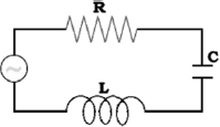
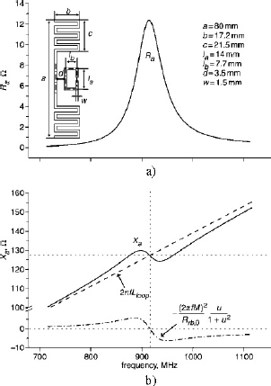
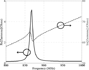
The efficiency analysis is based on the work presented in [CHO 07] for a simple meander-type tag structure (Figure 2.1) using a T-matching network to match a commercial tag chip located at the centre of the antenna.
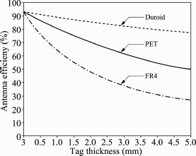
Three different substrate materials made of polyethylene terephthalate (PET) (εr: 3.9, tanδ: 0.03, thickness: 50 μm), Duroid (εr: 2.2, tanδ: 0.0009, thickness: 127 μm) and FR-4 (εr: 4.25, tanδ: 0.02, thickness: 1.6 mm) are used to examine the effect of the substrate material and thickness. The read-ranges for a given tag antenna size are shown in Figure 2.19. The read-range rapidly decreases as the antenna size is reduced since the radiation efficiency of the antenna drops. It is also clear that the use of high loss substrates such as FR-4 results in low antenna efficiencies and shorter read-ranges. By using thin substrates such as PET, the read-range of the tag can be greatly increased nearly to the value of the low-loss and high-cost substrate material, such as Duroid, despite the fact that the loss tangent of PET is about the same as that of FR-4. Figure 2.20 shows the radiation efficiency as a function of the substrate thickness for a given antenna size (kr = 0.6). As expected, the efficiency decreases as the thickness of substrate increases. For thin substrates (<0.4 mm), the loss tangent influence is reduced with a radiation efficiency over 80% for the three types of materials.
Figure 2.18. Geometry of the meander tag antenna used in the study of dielectric losses

Figure 2.19. Read-range versus antenna size and substrate materials. Δ: PET (50 μm); ![]() : Duroid (170 μm);
: Duroid (170 μm); ![]() FR-4 (1.6 mm)
FR-4 (1.6 mm)

Figure 2.20. Antenna efficiency versus substrate thickness and substrate materials:—— Duroid; — – — – PET; — — FR4
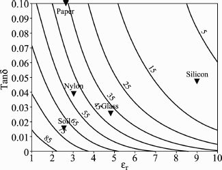
Finally, the antenna efficiency in Figure 2.21 is plotted when the tag is attached on different dielectric materials (all 2 mm thick) showing different permittivities and losses. Clearly, the efficiency decreases as the permittivity and loss tangent of the tagged objects are increased. These results show that the electrical properties of the tagged objects must be taken into account when designing the tag antennas.
Figure 2.21. Antennae efficiency versus dielectric properties of the tagged object
2.1.4.3. Analysis of the metallic losses
As the conductivity values are σ = 5.8 × 10⁷ S/m for copper and σ = 1.6 × 10⁶ S/m for silver ink, respectively, we expect reduced performances for silver ink printing [NIK 05]. The performance comparison between silver ink printing and copper etching is shown in Figure 2.22. The degradation of read range with the silver ink becomes more significant for small antenna sizes (kr < 0.5).
Figure 2.22. Read range versus antenna size and metal line conductivity. Δ: copper (σ = 5.8 × 10⁷S/m); ![]() : silver ink (σ = 1.6 × 10⁶ S/m)
: silver ink (σ = 1.6 × 10⁶ S/m)

Next, we examine the performance change due to a variation of the line thickness, as shown in Figure 2.23. The antennas are printed on PET substrate with copper metal-line whose thickness is varied between 0.1 and 5 μm. The read ranges decrease rapidly when the thickness of the copper line is less than 0.7 μm. As the thickness of metal-line is less than the skin depth (about 0.7 μm at 900 MHz for copper), significant conducting losses arise in the metal-line and the antenna efficiency is greatly reduced. From these results, we can see that the thickness of the metal-line should be larger than the skin depth for adequate readability.
2.1.4.4. Antenna detuning
In order to illustrate the effect of the dielectric material of the tagged object, the read range of the tag depicted in Figure 2.24 is given in Figure 2.25 as a function of frequency for an effective radiated power (ERP) of the reader ERP=2W [RAO 05]. Three configurations are considered: tag in free-pace, tag on Box 1, an empty cardboard box, and tag on Box 2, a cardboard box with plastic material εr = 2.87 inside. The read-range responses are shifted downward when the tag is put on either box because of the dielectric loading. Then, the tag is tuned by reducing the loading bar and the meander, as shown in Figure 2.24. The tuning differs for each box. The objective is to shift the read-range peak upward in the 868 MHz band. The presented tag design meets the desired range requirements (>2 m) for both boxes in 868 and 915 MHz frequency bands.
Figure 2.23. Read range versus metal line thickness

Figure 2.24. RFID tag using a loaded meander antenna. Tuning of the meanders and the bar for various box contents in 868 MHz band [RAO 05]
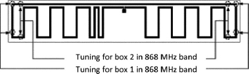
Figure 2.25. Variations of RFID tag range versus frequency for different tagged objects (ERP = 2 W). Box 1: empty cardboard box. Box 2: cardboard box with plastic material (εr = 2.87) inside

2.1.5. Near-field/far-field behavior of UHF RFID tags
In the previous sections, we have observed that a tag antenna can eventually be seen as the connection of a dipole-like antenna with a loop conductor. This loop is the result of the symmetrical association of two L-matching circuits. Concurrently, any small loop can be seen as a magnetic field sensor, whose sensitivity increases in proportion to the loop surface as shown below.
Let us consider the geometrical arrangement of the loop antenna of radius a, shown in Figure 2.26. A constant current I flows around the loop, which lies in the xy-plane and is centered at the origin. The near-field components are given by:
[2.35] 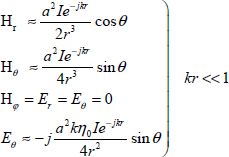
where k = 2π/λ is the propagation constant in free space, η0 is the wave impedance of free-space, r is the distance between the loop center and the observation point, and θ is the angle between the z-axis and the direction of the observation point. Hr and Hθ vary as 1/r3 while Eϕ varies as 1/r2. Therefore, as r is small, the H-field dominates the E-field in the near-field and the loop acts as a magnetic sensor.
Figure 2.26. Loop antenna and accompanying spherical coordinate system
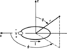
When the tag is in the vicinity of the reader antenna (say, up to 10 cm), it is actually located in the near-field of the reader antenna. The IC powering is mainly due to the magnetic flux across the loop while the dipole impact is weak. For larger distances, when the tag is in the far-field of the reader antenna, the dipole becomes a far-field sensor boosting the radiation resistance of the structure. This dual-behavior is stressed in Figure 2.27 where the loop is depicted as the near-field element and the dipole as the far-field element.
The same dual-behavior is used in a module combining a small loop and an RFID chip, the AK tag developed by the French company Tagsys (Figure 2.28). In a standard use, the AK tag is used for short-range communications (<50 cm), but its read range can be extended up to 10 m when the module is electromagnetically coupled to a resonant piece of metal. As the loop is used as a primary source and not as a dedicated matching element, bandwidth performance might be reduced, but the concept is so flexible and versatile that numerous industrial applications are possible.
Figure 2.27. Dual-behavior of a tag antenna: far-field and near-field elements
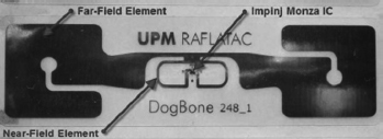
Figure 2.28. AK tag (Tagsys) using the UHF Gen 2 chip Monza 5. Frequency band 860–960 MHz; inlay dimensions: 12 mm × 10 mm

2.2. Matching between the antenna impedance and the microchip impedance
2.2.1. Matching conditions
Let us assumes that the IC impedance takes the form of the series combination of a resistance Ric and a reactance Xic and that the antenna is modeled by a linear source voltage Va, the source impedance being Za = Ra + jXa (see Figure 2.29). The power Pic delivered to the load Ric by the source is given by:
[2.36] ![]()
where Ia is the current flowing along the circuit. The maximum power transfer between the antenna and the load occurs if the matching conditions are fulfilled, i.e. when the source and load impedances are complex conjugates, Ric = Ra and Xic = –Xa. Under matching conditions, the power Pmax delivered to the tag IC is given by:
[2.37] ![]()
The power transfer coefficient (PTC) τ is then defined as:
[2.38] ![]()
The power delivered to the tag and the tag read-range are maximized for τ = 1. The magnitude |Γ| of the voltage reflection coefficient can be deduced from τ using
[2.39] 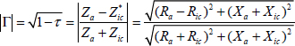
while the power reflection coefficient is |Γ|2 and the return loss is given by RL(dB) = −20 log |Γ|.
Figure 2.29. Circuit model of tag antenna and IC

The tag IC is usually represented as the parallel combination of some capacitance Ccp and some resistance Rcp that are related to the series capacitor Cic and resistance Ric through the following relationships:
[2.40] ![]()
[2.41] ![]()
Typical values provided by the main manufacturers (Alien Technologies, Impinj, NXP semiconductor, etc.) are around 1 kΩ for Rcp and 1 pF for Ccp. Therefore, the rough order of magnitude estimate is 7 for Qcp= RcpCcpω and 30 Ω for Ric in the UHF band.
2.2.2. L-matching basics
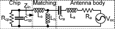
The great majority of commercial UHF RFID tags are based on dipole antennas using a modification of a T-match as a matching circuit. Most of the time, a T-match reduces to an L-match (Figure 2.30) as one of the series inductors can readily be included in the antenna reactance.
The series resonant frequency fa of the dipole is normally located above the working frequency f0 for miniaturization purposes. Also, fa>f0 allows us to reduce the influence of surrounding materials showing moderate permittivities. As a result, the dipole impedance at f0 is capacitive with typical resistances of a few dozen ohms and reactances ranging from roughly 100 to 200 Ω.
It is demonstrated in Figure 2.30 that an L-matching circuit based on two inductances Le and Lh is sufficient to match the impedance Zic of any UHF RFID IC with most dipole antennas found in RFID tags. Because Re(Zic) is small, the antenna impedance is always included inside the Re(Zic) = constant resistance circle. As a result, a proper combination of series and parallel inductances Le and Lh create the complex conjugate Zic* of the chip impedance. Typical inductances values range from few nH to few tens of nH and can be readily realized in microstrips.
Figure 2.30. Antenna matching to the UHF RFID IC with an L-match

2.2.3. Equivalent electrical circuits
Figure 2.31 shows a typical matching circuit for a commercial RFID tag with superimposed currents. In [DEA 09], the balanced circuit shown in Figure 2.31 can be fairly closely mapped to the unbalanced circuit shown in Figure 2.32, but mutual inductive couplings between Le and Lh and possibly La are neglected. Fortunately, any inductive coupling will serve to transform the antenna impedance, and will not, for example, disturb the antenna Q or resonant frequency. Thus, we can conclude that Figure 2.32 is qualitatively correct, although an exact translation between circuit element values and physical geometry is lost.
Figure 2.31. Commercial tag matching circuit with superimposed currents [DEA 10]

A series RLC circuit is used to model the antenna near resonance. Its resonant pulsation ωa and quality factor Qa are given by the well-known relationships:
[2.42] ![]()
[2.43] ![]()
Figure 2.32. Equivalent circuit of the double-tuned unbalanced tag
The circuit is then transformed into a more useful form as depicted in Figure 2.33 using the L-match transform identity in which the shunt-series inductors (Le and Lh) are replaced by the series-shunt inductors (Lse and Ln). The result of this transformation is a circuit that is in the canonical form of a two-stage bandpass filter with a series resonant circuit (Ra2, La2 + Lse and Ca2) and a parallel resonant circuit (Rcp, Ccp and Ln):
where
[2.44] ![]()
[2.45] ![]()
[2.46] ![]()
[2.47] ![]()
[2.48] ![]()
[2.49] ![]()
[2.50] ![]()
Figure 2.33. Equivalent circuit of the double-tuned unbalanced tag after L-match transformation. Circuit in the form of a two-stage bandpass filter
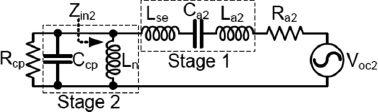
From Figure 2.33, we observe that the parallel resonance is independent of the radiating part. Therefore, the parallel resonance will not be directly affected by the dielectric environment of the tag. On the other hand, the series resonance will shift toward lower frequencies as the antenna electrical length increases with the dielectric permittivity.
2.2.4. Double-tuned matching
The practical implication of the circuit model described in section 2.2.3 is that a desired bandpass response can be synthesized with a proper calculation of the antenna impedance and the matching circuit [DEA 09]. We assume that the design parameters given are:
By tailoring the classic double-tuning theory to fit the model of Figure 2.33, the first condition of the optimum double-tune matching is to select the resonant frequency of the series and parallel tank circuits to be the same:
[2.51] ![]()
where ω0 is equal to the geometric mean of the band, i.e ![]() . It can be seen that Ln is entirely fixed by the chip reactance once ω0 is given.
. It can be seen that Ln is entirely fixed by the chip reactance once ω0 is given.
α is the remaining tuning parameter. Any change in α will change Lse and, thus, the series resonance. If we wish to change α, we will also need to modify ωa, the resonant frequency of the antenna, so that the resonant frequency of the series (Ra2, La2 + Lse and Ca2) circuit remains ω0. By combining [2.42] and [2.51], we obtain the following quadratic in ωa:
[2.52] ![]()
which is solved in the normal way. [2.52] can be rewritten in terms of La using [2.43]:
[2.53] ![]()
Finally, by applying the quadratic equation and considering only the positive inductances, we obtain the synthesized antenna inductance:
[2.54] 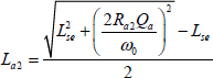
or equivalently:
[2.55] 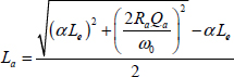
Finally, inductances are constructed from metallic flat or ribbon wire (rectangular cross section), using the following estimation:
[2.56] ![]()
where w and l are, respectively, the width and the length of the trace and t is the metallization thickness (all dimensions in cm). Once the previous values are fixed, it is possible to determine the reflection coefficient at ω = ω0 when both series and parallel tank circuits resonate:
[2.57] ![]()
or in terms of PTC:
[2.58] ![]()
In [2.57] and [2.58], |Γ| and τ are the worst reflection coefficient and the worst PTC, respectively, allowed through the bandwidth and observed at ω = ω0.
The optimum double-tuned match provides the maximum fractional bandwidth out of double-tuning [LOP 07]:
[2.59] 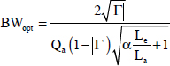
2.2.5. Synthesis of a double-tuned tag and a naïve tag
Let us assume an antenna with Qa = 15 which is approximately that of a meandering dipole with a length of 92 mm and a width of 8 mm. This size is popular in the high-volume commercial market, and thus conclusions drawn from this example are of commercial relevance. We let a typical Ra = 30 Ω and we assume the use of an IC with Rcp = 1500 Ω and Ccp = 1.2 pF for Qcp = 10.3. The goal is to maintain a 10 dB return loss, i.e. a power transfer efficiency of 90% between 860 and 960 MHz (worldwide operation in the Gen2 standard definition).
RL = 10 dB means that |Γ| =0.316 at f0 = ω0/2π = 908.6 MHz, the geometric mean of the UHF band. From [2.57], we obtain α = 0.196. Now ![]() implies that Le + Lh = 1/Ccp
implies that Le + Lh = 1/Ccp ![]() = 25.57 nH, and using [2.44] we find that Lh = 5.01 nH and Le = 20.56 nH. Knowing Lse and using [2.52] and [2.55], it is easy to find La=76.83 nH and fa = ωa/2π = 931.9 MHz to achieve Qa=15 and Ra=30 Ω. All circuit parameters including the optimized matching circuit (Le and Lh) are summarized in Table 2.3.
= 25.57 nH, and using [2.44] we find that Lh = 5.01 nH and Le = 20.56 nH. Knowing Lse and using [2.52] and [2.55], it is easy to find La=76.83 nH and fa = ωa/2π = 931.9 MHz to achieve Qa=15 and Ra=30 Ω. All circuit parameters including the optimized matching circuit (Le and Lh) are summarized in Table 2.3.
The next step is to design an antenna which resonates at 931.9 MHz with Qa = 15 and Ra = 30 Ω and fulfills the dimension constraints (92 mm × 8 mm). The wideband antenna geometry of Figure 2.34 proposed in [DEA 10] respects the conditions with a large number of meanders to achieve resonance. The simulated impedance Zin of the tag circuit (antenna + L-match) was obtained from an electromagnetic simulation of the tag using a method-of-moments (MoM) code. An excellent agreement was obtained between the simulated tag impedance and the tag impedance calculated with the circuit model.
Figure 2.34. Geometry of the wideband RFID tag
Table 2.3. Circuit parameters for the wideband and naïve antennas

The tag impedance calculated with the circuit model is plotted in Figures 2.35 and 2.36, along with the conjugate IC impedance. The imaginary parts Xin and Xic cancel out at three frequencies, i.e. 867, 902 and 948 MHz while the real parts Rin and Ric are equal at 879 and 935 MHz. Therefore, a perfect match does not occur at any frequency. The associated voltage reflection and power transmission coefficients are shown in Figure 2.37. The maximum transmission occurs at 876 and 942 MHz while a relative maximum of −10 dB is observed in-between at 908.6 MHz. The antenna does not achieve the 10 dB return loss over the entire 860–960 MHz band but covers 865–955 MHz, which is the practical band of worldwide operation. Both minima of the return loss correspond to frequencies where the IC and tag impedances partially match.
Figure 2.35. Resistance of the wideband tag and the IC

Figure 2.36. Reactance of the wideband tag and complex conjugate of the IC reactance

For comparison, a “naïve” short antenna resonating at a much higher frequency fa = 1,050 MHz is designed to present a conjugate match to the IC at f0 = 908.6 MHz. This antenna presents the same parameters Qa = 15 and Ra = 30 Ω as the wideband antenna. From [2.43], we extract the two remaining parameters La = 68.2 nH and Ca = 0.337 pF.
Using the method described in section 2.2.2, we first calculate Lh so that Re(Za/j Lhω0) = Re(Zic) at f0. We find Lh = 9.77 nH. Then, Le is obtained from:
[2.60] ![]()
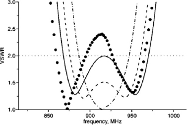
which yields Le = 9.53 nH. The resulting input impedance Zin is plotted on Figures 2.38 and 2.39 along with the conjugate IC impedance while the corresponding power reflection and power transmission coefficients are plotted on Figure 2.37. The naive design shows a perfect match at the nominal frequency 908.6 MHz but much more narrowband behavior than the wideband tag and provides only 27 MHz of 10 dB return loss. This suggests an improvement in bandwidth by a factor of about 3.3 using the double-tuning method.
Figure 2.37. Power transfer coefficient (PTC) and power reflection coefficient (Γ) versus frequency for the wideband tag (plain line) and the naïve tag (dotted line)

Obviously, we can achieve much better return loss over a narrower frequency band than the wideband tag. For example, a return loss of 14 dB can be achieved between 865 and 930 MHz (covering the vast majority of worldwide operations, including North America and Europe) using the proposed approach.
Figure 2.38. Resistance of the naïve tag and the IC
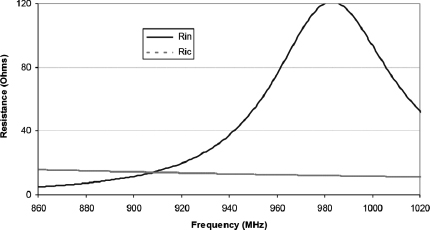
Figure 2.39. Reactance of the naїve tag and complex conjugate of the IC reactance

2.2.6. Alternative implementation of the optimum double-tuned match
The tag synthesis described in the previous section relies on the ability to design an antenna from the knowledge of the lumped-elements Ra, La and Ca. As a result, circuits used to model complex antenna geometries are useful abstractions but it is not easy to synthesize a specific geometry from a circuit. At least, it is beyond the capability of commercial full-wave simulators. On the other hand, the design approach proposed in [XI 11] is based on the input impedance of the whole tag antenna (i.e. the antenna body plus the matching network). According to Figure 2.32, the resistance and reactance of the tag antenna are given by:
[2.61] 
[2.62] ![]()
By taking the first-order derivate of Rin with respect to ω, it is found that Rin maximizes at the frequency given by
[2.63] 
The corresponding values of Rin and Xin at ω = ωmax are given by
[2.64] 
[2.65] ![]()
Using these two expressions, the following design procedure is proposed in [XI 11]:
2.2.7. Example of a double-tuned match tag and use in variable environments
To validate the alternative implementation described in 2.2.6, a double-tuned antenna has been built in [XI 11]. As shown in Figure 2.40, the proposed tag antenna is a loaded meander line dipole made in copper, with a total size of 93 mm × 11 mm. The matching network adopts a T-match structure, where W1 can be adjusted to tune Lh. W2 and H2 can be adjusted to change Le. The loading bar (i.e. the horizontal trace beneath the meander line) provides extra freedom to control Ra. The tag chip used in this paper is Alien Higgs-3 (Rcp =1.5 kΩ, Ccp= 0.85 pF). A parallel stray capacitance of 0.3 pF is included to account for the imperfect connection between the tag antenna and the chip strap.
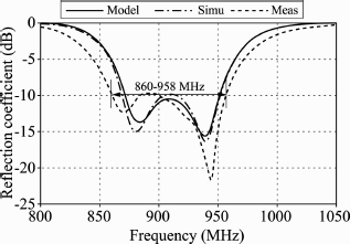
A method-of-moments (MOM) full-wave simulator, IE3D, is used to assist the design. The proposed antenna is optimized for working on paper characterized by εr=2.3, loss tangent=0.1 and thickness=0.16 mm. The optimized dimensions and lumped-element model of the proposed antenna are listed in Tables 2.4 and 2.5, respectively. The lumped-element model is extracted from simulation results by curve-fitting. Results of modeling, simulation and measurement are compared in Figures 2.41 and 2.42 with respect to antenna impedance and return loss, respectively. The double-tuning effect can be clearly seen in the return loss plot. The 10-dB bandwidth is estimated to be 9.3% by implementing the data of Table 2.3 in equation [2.21], which is close to the measured result – 10.8%, which is close to the measured result – 10.8%. The difference between simulation/modeling and measurement is mainly due to the additional loss in the measurement and the uncertainty in the electromagnetic properties of the paper substrate.
Figure 2.40. Geometry of the proposed antenna: a) parameter definitions and b) photo of the prototype
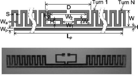
Table 2.4. Dimensions of the antenna (in mm)
Table 2.5. Lumped-element model of the antenna

Figure 2.41. Input impedance of the proposed antenna
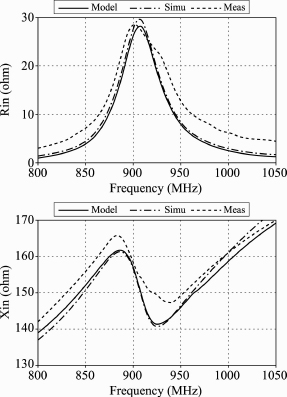
Figure 2.42. Return loss of the proposed antenna
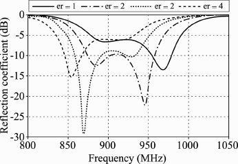
The sensitivity to the dielectric loading is studied by both simulation and measurement. The simulation studies the influence of the dielectric permittivity on the bandwidth. During this simulation, loss tangent and thickness of the dielectrics are fixed as 0.1 and 0.16 mm, respectively. As shown in Figure 2.43, the acceptable matching (i.e. return loss < –6 dB) tends to disappear when the permittivity is larger than 4. Since the infinite dielectric model used in the IE3D simulator generally overestimates the dielectric loading effect, the proposed antenna should be more tolerant than what Figure 2.43 indicates.
The chip strap is mounted onto the tag antenna with conductive adhesives and the maximum reading distance is estimated with the Tagformance RFID tester from Voyantic [OCO 09]. In Figure 2.44, the measured tag responses are plotted within the world UHF RFID band (i.e. 860~960 MHz) on diverse materials. Read ranges generally stay between 8~12 m except on a book where high loss is encountered. Figure 2.44 also illustrates the double-tuning effect since the shape of the read range curves follows that of the PTC.
Figure 2.43. Simulated return loss of the proposed antenna on dielectrics of different permittivities
2.3. RFID tag antennas using an inductively coupled feed [SON 05]
This section presents a design methodology to make efficient and wideband RFID tag antennas using an inductively coupled feed. An analytical model for the inductively coupled feed is presented first. Then, the main rules to achieve wideband impedance match between the antenna and the chip are presented.
Figure 2.44. Measured read-range on diverse materials
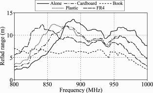
Figure 2.45. a) Inductively coupled feed structure, b) equivalent circuit, c) example of AKA kernel (loop + IC) commercialized by Tagsys RFID

2.3.1. Analytical model
The proposed feed structure is shown in Figure 2.45(a) along with dimensional notation. The antenna is composed of a small rectangular loop and a radiating (or resonant) body, which are coupled inductively. Two terminals of the loop are directly connected to the chip. The strength of the coupling is controlled by the distance between the loop and the radiating body, as well as the shape of the loop. Figure 2.45(b) also depicts the equivalent circuit of the inductively coupled feed structure. The inductive coupling is modeled by a transformer. The input impedance of the antenna Za is
[2.66] ![]()
where Zrb and Zloop are the individual impedances of the radiating body and the feed loop, respectively. M is the mutual inductance between them, which can be roughly derived analytically on the assumption that the radiating body is infinitely long.
[2.67] ![]()
Near the resonant frequency f0 of the radiating body, its impedance can be expressed using the radiation resistance Rrb,0 and the quality factor Qrb as a function of
[2.68] ![]()
The impedance of the feed loop is as follows:
[2.69] ![]()
where Lloop is the self-inductance of the feed loop. The resistance and reactance components of Za are finally given by:
[2.70] ![]()
[2.71] ![]()
where u= Qrb.(ω/ω0 - ω0/ω). At ω = ω 0, the components of Za,0 become:
[2.73] ![]()
Equations [2.72] and [2.73] show that Ra,0 depends only on M, while Xa,0 is dependent only on Lloop. Therefore, Ra,0 and Xa,0 can be adjusted independently. This means that the proposed feed structure presents a simple and easy way to match an antenna impedance to an arbitrary chip impedance Zc = Rc + jXc. Figure 2.45(c) depicts a universal low-cost “adaptive kernel” that can act as a high-performing secondary antenna.
2.3.2. Antenna design and results
An example of the antenna using the proposed feed structure is shown in the inset of Figure 2.46 with the detailed dimensions. The antenna was designed for an RFID tag chip with Zc = 6.2‒j127 Ω. The resonant frequency f0 of the radiating body is 915 MHz. Simulated data of Rrb,0 =28.5 Ω and Qrb=14.7 are obtained using CST MW Studio.
Figure 2.46. Antenna impedance versus frequency: a) resistance component Ra and b) reactance component Xa
The calculated values of M and Lloop are 3.3 and 22.1 nH, respectively. Figure 2.46(a) shows the resistance component Ra as a function of frequency, for which the maximum value is Ra,0 = 2Rc at f = f0. Figure 2.46(b) shows the reactance component Xa, which equals ‒Xc at f = f0. The first term of the right side in equation [2.72] is a straight line with positive slope and the second term has negative slope in the range f0 ± f0/(2Qrb). Therefore, the first and second terms cancel each other, and it makes the inductively coupled feed structure have wideband characteristics.
VSWR versus frequency is shown in Figure 2.47 with variation of Ra,0, where Ra,0 can be adjusted by simply altering the distance between the radiating body and the feed loop without any change of Xa,0. The plot indicates that the impedance bandwidth for VSWR < 2 becomes maximum value when Ra,0 = 2Rc. The antenna was fabricated and measured for validation. It was printed on a thin flexible polyethylene substrate with a thickness of 50 μm using copper traces with a thickness of 18 μm. Figure 2.47 also shows the measured VSWR of the antenna, which closely agrees with the calculated one.
Figure 2.47. VSWR versus frequency for different values of Ra,0:—Ra,0 = 2Rc, – – – Ra,0= 2.5Rc, —′′ —Ra,0 = Rc, ![]() measurements
measurements
2.4. Combined RFID tag antenna for recipients containing liquids
The close environment of UHF RFID tags, i.e. the medium on which the inlay is fixed (plastic, metal, cardboard) and its contents (liquids, highly dielectric, metalized, etc.), degrades the radiation pattern, the antenna matching to the integrated circuit and the overall tag efficiency. This, added to the obstructions and multipath effects in indoor environments, can dramatically reduce the read-range between the reader and the tag.
The objective is to design a tag antenna attached to a plastic recipient that may be empty or filled with a liquid. A small-loop-based module excites two dipole antennas through inductive coupling. Each antenna is designed to work either for the filled or for the unfilled case at 868 MHz (UHF band).
2.4.1. Module description
The MuTRAK640 module manufactured by Tagsys is essentially the series connection of a small-loop antenna with a UHF RFID chip, the Impinj Monza 4. The measured chip read sensitivity and the input impedance are ‒14.7 dBm and 1100 Ω//2.11 pF, respectively [SAB 12]. Let Zc = Rc + jXc be the series equivalent impedance of the chip load (Zc=6.8 Ω -j86 Ω at 868 MHz). The circuit is encapsulated in a rectangular housing made up of FR4 epoxy. A key point is that the small loop dimensions yield a radiation resistance less than 1 Ω. Therefore, the loop only allows short-range reading distances (few centimeters) restricted to the reactive near-field region.
A useful feature of the module is that it can be used as a primary excitation for larger tag antennas. The idea is that a small device basically developed for short reading distances because of its low radiation resistance also performs well at distances up to 10 m when coupled with a dipole-like antenna. Typically, the magnetic field normal to the loop surface turns around the dipole located at a close proximity to the module and generates a current in the dipole. The dipole boosts the module radiation by increasing its radiation efficiency.
Figure 2.48. Spiral dipole coupled to the MuTRAK module (loop+chip). Initial dimensions of the spiral dipole working in free space: L1= 40 mm, L2=20 mm, L3=13.5 mm, L4=16.5 mm, L5=10 mm, L6=13.5 mm, L7=3.5 mm, wire radius= 0.15 mm. Total length: 181 mm
2.4.2. Inductive coupling and antenna matching
As seen in 2.3.1, the excitation of a dipole by an inductively-coupled loop yields the following impedance seen from the chip terminals [SON 05]:
[2.74] ![]()
The above expression includes the mutual coupling factor M caused by the proximity between the dipole and the small loop, and the dipole impedance Zdipole besides the loop impedance Zloop. From [2.74], it can be observed that the series resonance of a half-wavelength dipole is transformed into a parallel resonance at the loop terminals. Equation [2.75] gives the power wave reflection coefficient of the antenna normalized to the antenna resistance [NIK 05a].
2.4.3. Antenna design
The maximum PTC between the antenna and the chip will occur for Zantenna = Zc*. Apart from the compensation of the chip capacitance by the antenna inductance, it is also necessary to keep a low antenna resistance. A dipole with spiral inductors at its ends is coupled to the encapsulated circuit MuTRAK, as shown in Figure 2.48. Spiral dipoles are compact and more efficient than zig-zag or meandered dipoles, as large gaps between the parallel segments are introduced. The dipole was made up of a thin copper wire that is fixed on a piece of paper to keep the antenna shape and rigidity. The dimensions of the dipole are given in Figure 2.49. The distance between the module edge and segment L1 is 2 mm.
Figure 2.49. Impedance of the loop-coupled spiral dipole
The loop-coupled spiral dipole antenna is designed to resonate at 868 MHz. All simulations are performed with the 4NEC2 code based on the MOM. The simulated impedance is Zantenna = (5.1 + j62) Ω for the required frequency (Figure 2.49). The estimated gain is 0 dBi. Coupling the dipole to the module introduces a parallel resonant at the chip terminals at 868 MHz as observed in Figure 2.48. As a result, the antenna impedance shows a higher radiation resistance and a flatter reactance approximately 868 GHz compared to the loop impedance. However, the reactance mean value is essentially the loop reactance that is too low at 868 MHz to exactly compensate the ‒86 Ω reactance of the chip. Therefore, even though the comparable antenna and chip resistances result in a Γ minimum, the total reactance (approximately ‒24 Ω) is large compared to the total resistance (approximately 12 Ω) which leads to Γ = 0.89. This means that the read-range which would be obtained for a perfect match is divided by ![]() . This mismatch is inherent to the module resonance centered at 915 MHz, not to the design procedure. The following tag resonance is due to the cancellation of the total reactance and occurs above 1,000 MHz, i.e. much higher than the module resonance as the dipole coupling reduces the reactance of the isolated loop.
. This mismatch is inherent to the module resonance centered at 915 MHz, not to the design procedure. The following tag resonance is due to the cancellation of the total reactance and occurs above 1,000 MHz, i.e. much higher than the module resonance as the dipole coupling reduces the reactance of the isolated loop.
2.4.4. Measurements of the initial tag
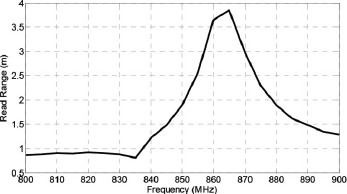
Measurements of the dipole resonant frequency are performed with the King’s shielded loop [KIN 69] used as a near-field sensor in the vicinity of the dipole. This particular probe avoids external sheet currents on the measurement cable. The dipole resonance is observed on a vector network analyzer at the King’s loop terminals. The dipole length is adjusted to resonate at 868 MHz yielding the dimensions given in Figure 2.48. Then, the MuTRAK module is implemented and read-range measurements are performed with the help of the Voyantic Tagformance measurement system [OCO 09]. The tag read-range measured in the 800–900 MHz band (Figure 2.50) shows a maximum of 3.8 m at 868 MHz. This is in agreement with the estimated read-range using the modified Friis formulation given in [NIK 05a].
Figure 2.50. Read-range measurements with the Voyantic setup
2.4.5. Measurements with an empty and filled plastic recipient
The spiral antenna described previously is placed on an empty plastic polypropylene (εr = 4) recipient whose size is 23 cm × 15.5 cm × 14.5 cm. Due to the plastic wall, a 60 MHz negative shift of the resonant frequency is measured. To adjust the resonance frequency, the wire length is reduced gradually and symmetrically shortening the wire until the correct resonant frequency is obtained. A total length of 12.5 mm is finally removed from the dimensions given in Figure 2.50 (L7 = 0, L6’ = 5.5 mm). The maximum read-range drops at 3.7 m.
Once the recipient is filled with fresh water (εr = 80, σ = 0.1 S/m), tag detection is not possible even at few centimeters from the reader. Using the King’s shielded loop, a 550 MHz negative frequency shift of the dipole resonance is first determined. An additional 19 mm length reduction is necessary to resonate at 868 MHz (L7, L6 and L5 equal to zero and L4’=13 mm). In the presence of water, the maximum read-range is 34 cm.
2.4.6. Combined antenna
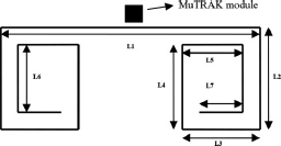
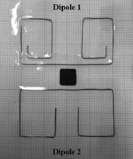
The final tag combines both proposed antennas and the MuTRAK module as shown in Figure 2.51. As the dipole resonant lengths are very different, no direct coupling between the dipoles is observed and each dipole behaves as if it was alone. Dipoles 1 and 2 resonate with the empty and filled recipient, respectively. Without water, the maximum read-range remains around 3.7 m. In the presence of water, the read-range is reduced to 31 cm, i.e. 3 cm shorter than for the single dipole. In any case, this is a strong improvement compared to the single antenna designed for the empty recipient where no detection is observed for any distance. The concept can be applied to other liquids or recipient materials as long as only two states (filled or unfilled) are considered. The tag read-range could be doubled with the MuTRAK650 version of the module based on a 3 dB more sensitive chip (Monza 5) and optimized loop dimensions.
Figure 2.51. Combined antenna structure
2.4.7. Discussion relative to the respect of the matching conditions
The matching conditions must be simultaneously fulfilled for the real and imaginary parts of the input impedance of the antenna; in other words, matching is obtained when Rantenna = Rc and Xantenna = ‒Xc. It is desired to study the power reflection Γ in [2.75] when only one of the two conditions is respected. To facilitate this study, ![]() is plotted in Figure 2.52 as a function of Rantenna for different values of Xantenna with Rantenna varying around its optimal value Rantenna = 6.8 Ω. Ιn Figure 2.53, Γ is plotted as a function of Xantenna for different values of Rantenna with Xantenna varying around its optimal value Xantenna = 86 Ω.
is plotted in Figure 2.52 as a function of Rantenna for different values of Xantenna with Rantenna varying around its optimal value Rantenna = 6.8 Ω. Ιn Figure 2.53, Γ is plotted as a function of Xantenna for different values of Rantenna with Xantenna varying around its optimal value Xantenna = 86 Ω.
Figure 2.52. Power reflection versus antenna reactance with Zic = (6.8‒j86) Ω and for various antenna reactances : Xa=60 W——, Xa =75 W — – — Xa=81 W – – –, Xa=86 W ----

Figure 2.53. Power reflection versus antenna reactance with Zic = (6.8‒j86) Ω and for various antenna resistances Ra=1 W——, Ra =3 W–— – —, Ra=6.8 W – – –, Ra=20 W–

In Figure 2.52, we first observe that once the matching condition is respected on the imaginary parts, the tolerance around the antenna optimal resistance Rantenna = Rc = 6.8 Ω is large. We noted that Γ remains below -10 dB, roughly for Rc/2 < Rantenna<2 Rc.
Conversely, Figure 2.53 indicates that once the matching condition is respected on the real parts, the tolerance around the antenna optimal reactance Xantenna = Xc = 86 Ω is small. We noted that Γ remains below ‒10 dB, roughly for 0.95Xc < Xantenna<1.05Xc.
We conclude that, given the typical impedances of RFID chips where series reactances are 5 to 10 times larger than series resistances, the respect of the matching condition on the imaginary part is crucial.
We also noticed that when the matching condition is far from being respected for the reactances, it is better to have Rantenna ![]() 6.8Ω as
6.8Ω as ![]() tends to be less degraded than for small Rantenna values (see curve Rantenna = 20 Ω for Xantenna < 70 Ω or Xantenna > 100 Ω in Figure 2.53).
tends to be less degraded than for small Rantenna values (see curve Rantenna = 20 Ω for Xantenna < 70 Ω or Xantenna > 100 Ω in Figure 2.53).
2.5. Tag on metal
RFID tags not only need to be mounted on non-metallic objects, but also on metallic objects. There is a strong interest from many industries (airplane, automotive, construction, etc.) in tagging metal items (airplane or automotive parts, metal containers, etc.) [ERG 07]. More generally, metal tags are usually more environmentally resistant than non-metal tags. For the tracking of high-value assets, such as industrial machinery, relatively large and complex antenna structures are acceptable to guarantee the required performance, but miniaturization approaches are needed to achieve the seamless integration of the tags with small everyday metallic items.
However, degradation in the performance of RFID tags is inescapable because of high-parasitic capacitance between the metallic surface and the antenna when tags are placed on metallic objects [UKK 05, CHO 08]. This degradation affects the radiation efficiency of the tag antenna, its radiation pattern and the input impedance. Figure 2.54 shows the effect of the gap between a metal plate and a dipole-based tag antenna. To improve the radiation efficiency and gain of tag antennas on metallic surfaces, some patch types and inverted-F types have been designed on thick and rigid substrates at high cost and with short read-range [RAO 08, KWO 05]. These antennas use shorting-pins or shorting-walls, which make their fabrication cost much higher than that of normal label-type antennas.
A key point is that metal tags require some thickness. In other words, they protrude from the mounting surfaces more or less. It is strongly desired to reduce the thickness of metal tags so as to make them more flexible in application and more aesthetic in appearance. To make these tags suitable for low-cost mass production, they should have a simple, thin structure, which is easy to fabricate from inexpensive materials.
The thicknesses of these existing designs vary from 0.8 to 2 mm. However, a thickness around 1 mm is still not small enough for tagging modern IT assets (e.g. the thickness of the latest Apple MacBook Air is less than 3 mm). Moreover, the thickness makes it difficult to curve tags for mounting on metallic cylinders (e.g. gas tank, fire extinguishers). These applications will motivate new developments on reasonably efficient solutions of ultra-low profile metal tags with thicknesses ranging from 50 μm to 300 μm.
In the following section, efficiency issues regarding low-profile patch antennas are first described. Then examples of ultra-thin and thick UHF tags are described with emphasis put on the design process, chip matching strategies and antenna performances in terms of overall efficiency.
2.5.1. Radiation efficiency of low-profile patch antennas [XI 13]
Radiation efficiency η = Prad/Pin is the ratio of power Prad radiated into the space and the power Pin injected into the antenna. For patch antennas, any power consumed by the antenna other than the space-wave radiation can be classified into three loss mechanisms: dielectric loss, conductor loss and surface wave loss. For the RFID frequency bands, the substrate thicknesses are much smaller than the wavelength in the substrate so that losses in surface waves are negligible. The following compact expression for radiation efficiency [VOL 07] can eventually be determined:
[2.76] 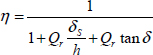
where σ is the metal conductivity, f is the working frequency, μ0 is the permeability in free space and
[2.77] ![]()
is the conductor skin depth. Qr is the radiation quality factor. Its analytical expression as a function of the patch dimensions and substrate permittivity is found in [JAC 91] where it is shown that Qr is inversely proportional to the substrate thickness and proportional to the substrate permittivity. The term Qrδs/h is the power ratio of the conductor losses to the radiated power. The term Qrtan δ is the power ratio of the power lost in dielectric losses to the radiated power.
Note that the efficiency reduces for “bad” conductors (where σ is poor and εs is small) and “bad” substrates (tanδ is high). It is also clear from [2.76] that:
To quantitatively demonstrate the influence of the substrate thickness, the radiation efficiency of a generic rectangular patch antenna is studied [XI 13]. The length and width of the patch antenna are 99.9 mm and 45 mm, respectively. Feeding point is at the center of one radiating edge. Calculated radiation efficiency is obtained with [2.76], while a simulated result is provided by HFSS. During simulations, a 300 mm × 200 mm metal plate is used as the ground plane, and a σ=4 × 10⁸ S/m finite-conductivity boundary is defined to model the conductors. The substrate is a type of PET plastic, whose electric properties are εr = 2.62, tanδ = 6.84×.0-3.
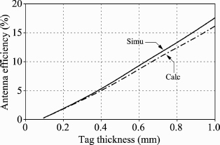
First, the radiation efficiency is studied as a function of the substrate thickness at the antenna resonance frequency (925 MHz for patch antennas studied, though it slightly varies with the substrate thickness). As shown in Figure 2.54, the agreement between the simulation and the calculation is perfect. The radiation efficiency monotonically decreases as the substrate thickness decreases.
Figure 2.54. Simulated and calculated radiation efficiency as a function of substrate thickness [XI13]
Next, the frequency response of the radiation efficiency is studied at three substrate thicknesses. In addition to the normal case including all loss mechanisms, two special cases where the dielectric loss and the conductor loss are excluded, respectively, are evaluated. To simulate the radiation efficiency without the dielectric loss, tan´ of the substrate is set to 0. To simulate the radiation efficiency without the conductor loss, a perfect electric-conductor (PEC) boundary is used instead of the finite conductivity boundary in HFSS. According to the simulation results shown in Figure 2.55, the frequency response of the radiation efficiency is generally quite flat, especially when all losses are included. By comparing the three cases at each substrate thickness, it is found that, at a large substrate thickness (e.g. h = 0.855 mm), the influence of the dielectric loss on the radiation efficiency is greater than that of the conductor loss. At a medium substrate thickness (e.g. h = 0.513 mm), the influences of the two loss mechanisms are comparable. At a small substrate thickness (e.g. h = 0.171 mm), the influence of the conductor loss exceeds that of the dielectric loss.
We finally conclude that a successful implementation of ultra low-profile patch antennas at extremely small thicknesses requires a good conductor. Thus, it is hardly possible to adopt conductive inks here.
2.5.2. Ultra-thin metal tags
This section describes two antenna designs specifically developed for thin substrates (h <1 mm) including either their own ground plane or using their support as a ground plane.
The first design is an inset-fed patch integrated with short-circuited transmission line [XI 13] where the real part and the imaginary part of the antenna impedance can be adjusted independently (Figure 2.56). The inset feeding allows the antenna resistance tuning, while the reactance is controlled by the short-circuited transmission line loading. Around the TM10-mode antenna resonance frequency, the impedance behavior of the proposed tag antenna can be modeled by a lumped-element equivalent circuit as shown in Figure 2.57. In the model, the parallel RLC tank (i.e. Ra, La, Ca) models the inset-fed patch, while the series-connected inductor (i.e. Lt) models the short-circuited transmission line. According to the antenna model, a typical plot of the antenna impedance is shown in Figure 2.58.
The short-circuited transmission line loading is used for the adjustment of the imaginary part of the antenna impedance. According to Figure 2.58, it is a good to start trying to compensate for the chip capacitance Xic with Xmax. Using the antenna model shown in Figure 2.57, it can be opined that Xmax satisfies the following equation:
Figure 2.55. Simulated and calculated radiation efficiency as a function of frequency for three substrate thicknesses [XI 13]
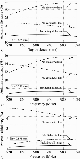
Figure 2.56. Inset-fed patch integrated with short-circuited transmission line [XI 13]
Figure 2.57. Lumped-element model [XI 13]

Figure 2.58. Input impedance of the antenna [XI 13]

Equation [2.78] is also illustrated in Figure 2.58. Therefore, Lt and Ra need to be adjusted in order to realize the desired Xmax. Out of the geometry variables of the proposed tag antenna, Ln and Wf are two key variables to control Lt. For the adjustment of Ra, the inset feeding is used. Ra decreases as the feed approaches the center of the patch. To take care of the remaining task for the conjugate match (i.e. to make real parts of the tag antenna and the tag chip equal), a proper Ln needs to be found so that Ra/2 equals the chip resistance.
The tag chip used in [XI13] is Alien Higgs-3. According to the impedance matching strategy described above, three metal tag antennas have been designed for substrate thicknesses of 0.855, 0.513 and 0.171 mm, respectively. Their sizes are all 99.9 mm × 45 mm. Material parameters used for these antenna designs are the same as those used in section 2.5.1. Simulated and measured return losses (RL) of the three designs, regarding the chip impedance, are shown in Figure 2.59. Due to double-tuning, the impedance bandwidths with h = 0.513 and 0.171 mm are larger than that with h = 0.855 mm.
Figure 2.59. Return loss for the three antenna thicknesses

For “thick” substrates (say, h > 1 mm in the ultra high frequecy (UHF) RFID band), the frequency response of the radiation efficiency is stable across a very wide frequency band. Therefore, there is no need to look at the radiation efficiency bandwidth, which is much larger than the impedance bandwidth. However, for the proposed ultra-low-profile metal tag antenna, the situation changes significantly. Simulated radiation efficiency of the three tag antennas is shown in Figure 2.60. Peaks clearly emerge at the corresponding antenna resonance frequencies. Note that the antenna resonance frequency shifts a bit higher from approximately 925 MHz to about 942 MHz due to the notch in the inset-fed patch.
Figure 2.60. Simulated radiation efficiency of the tag antenna designs as a function of frequency

For a given substrate thickness, the narrowest radiation efficiency bandwidth always happens when only accounting for the conductor loss. It implies that the conductor loss is more frequency dependent than the dielectric loss. At extremely small substrate thicknesses, the radiation efficiency bandwidth can be much narrower than the corresponding impedance bandwidth.
We conclude that when some feeding structure is added to the generic patch antenna to match the impedance of tag chips, the radiation efficiency bandwidth suffers from a significant shrinkage. As the substrate thickness decreases, the shrinkage in the radiation efficiency bandwidth becomes severer. As a result, at extremely small substrate thicknesses, it is necessary to take into account the radiation efficiency bandwidth.
Figure 2.61. Measured read-range of the tag prototypes
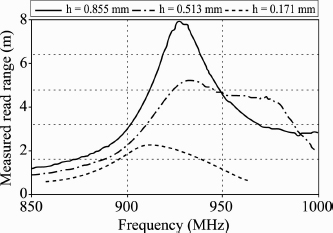
The read-range of the tag prototypes is measured after placing tags on a metal plate of 300 mm × 200 mm. Measurement results of the read-range are shown in Figure 2.61. The maximum read-ranges with h = 0.855, 0.513 and 0.171 mm are 7.9, 5.1 and 2.2 m, respectively. It is interesting to find that the maximum read-range is approximately proportional to the substrate thickness. When h = 0.855 mm, the read-range bandwidth is determined by the impedance bandwidth. When h = 0.171 mm, the read-range bandwidth is restricted by the radiation efficiency bandwidth. In other words, for metal tag antennas implemented at extremely small substrate thicknesses, the frequency response of the read-range is shaped by the radiation efficiency rather than the power transfer coefficient.
The second design is a dual-band RFID antenna that can cover both the 866 MHz band used in Europe and the 915 MHz band used in North and South America. The configuration of the antenna is illustrated in Figure 2.62. The antenna consists of two patch arrays: A1A2 for 866 MHz and B1B2 for 915 MHz, and an ultra-thin flexible substrate polypropylene (PP) with a ground plane. Since the thickness of the flexible substrate PP (εr = 2.4, tan δ = 0.02) is only 0.55 mm, which generally leads to a small read-range, the arrays are designed to increase the gain of the tag antenna. The two patch arrays A1A2 and B1B2 are both symmetrical about the origin in order to conveniently connect the dual independent ports of the Monza 4 tag chip (chip ports connect: port1 “RF1”+ “RF1” – connected to A1A2 and port2 “RF2”+ “RF2” – connected to B1B2). The two patch arrays are all short-circuited to the ground at the two ends of the substrate so that the size of patches Lp = 43.6 mm can be compacted as a quarter wavelength resonant antenna compared with a half-wavelength resonant antenna.
Although the resonant frequencies of the antenna are dominated by the length of patch Lp, the frequency difference between two bands is affected by parameters Wp1 and Wp2 (Wp1 is the width of A1 and A2 for 866 MHz and Wp2 is the width of B1 and B2 for 915 MHz). Furthermore, by adjusting the length of slots l1, l2 and Ls, the input impedances of dual ports can be conjugate matched easily. The actual overall size of the antenna is L × W = 90 × 30 mm2. The optimal design parameters are as follows: Wp1 = 14 mm (866 MHz), Wp2 = 11 mm (915 MHz), Wp3 = 3.4 mm, Ls = 39.5 mm, l1 = 10.2 mm (866 MHz), l2 = 5.5 mm (915 MHz), S1 = 0.5 mm, S2 =0.8 mm, S3 = 1 mm and Wline = 1 mm.
Figure 2.62. Geometry of the dual band antenna
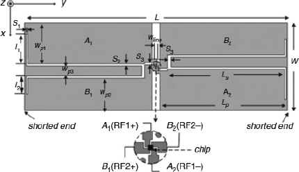
Figure 2.63 shows that the Europe band (865–868 MHz) is covered by a –20 dB bandwidth of 3.5% (847 – 877 MHz) while the North America band (902–928 MHz) is covered by a –20 dB bandwidth of 5.6% (877–930 MHz). The authors claim that the –10 dB bandwidth of the proposed structure is wider than that of the conventional microstrip patch antenna. It is likely that the antenna efficiency is very low (few percents) as the calculated gain is –10 dB. The maximum read-range is 3.5 m at 866 MHz and 3.6 m at 915 MHz when the antenna is mounted on a 150 × 150 m2 metal plate (Figure 2.64). Furthermore, the read-range curve confirms that the proposed antenna has not only a dual-band property, but also balanced read-range performance at each band.
Figure 2.63. Measured and simulated return loss of the dual-band antenna

Figure 2.64. Measured read-range of the dual-band antenna
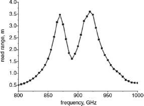
2.5.3. Thick metal tags
This section describes two topologies of modified RFID patch antennas built on low-cost thick substrates with thicknesses greater than 2 mm.
The first antenna makes use of a pair of u-shaped slots (Figure 2.65) to excite two adjacent resonant modes with similar radiation characteristics at frequencies close to each other, resulting in a wide-bandwidth patch antenna. The rectangular patch has dimensions of 40 × 86 mm2, and is printed on an FR4 substrate (εr = 4.4) with a thickness of 2 mm. The microstrip feed line is deep inset into the patch to decrease the input impedance. The feed line is divided into the inset feed line (length 8 mm) and the short stub line, between which the microchip is attached. The short stub line is short-circuited to the ground plane by a via hole. A pair of U slots is etched on the patch close to and parallel to the non-radiating edges of the patch. By embedding the pair of U slots, a new resonant mode between the TM10 and TM20 modes is excited.
Figure 2.65. Geometry of the dual-band antenna with a pair of U slots

The impedance matching between the antenna and the microchip at the frequency of the TM10 mode can be tuned by adjusting the inset length (Linset) and the distance (Ls) between the microchip and the via hole. On the other hand, the impedance matching at the frequency of the new resonant mode can be tuned by adjusting the slot arm length (Larm), the slot width (d) and the distance (dw) between the slot and the patch edge. With the increase of Larm, the new resonant mode frequency decreases to the TM10 mode frequency. With the decrease of d and dw, the impedance resonant amplitude of the new resonant mode could be decreased. The impedance of the microchip is 13.l–j64 Ω at 866.5 MHz and 13.5–j60 Ω at 915 MHz. When the dimensions are properly chosen as Linset = 38 mm, Ls = 17 mm, Larm = 9.5 mm, d = 0.6 mm and dw = 1 mm, the new resonant mode is excited near the TM10 mode and both resonant modes have good impedance matching. In this way, a broadband characteristic can be attained for the antenna.
Figure 2.66 shows the simulated impedance of the proposed antenna with different arm lengths (Larm). Note that the frequency f1 is the TM10 mode and f2 is the new resonant mode excited by the U slots between the TM10 and TM20 modes. With the increase of the arm length Larm, f2 decreases rapidly to f1 while f1 is slightly affected. When the arm lengths are properly chosen, the resonant mode of f2 can be excited at the frequency that is close enough to f1 to form a wide operating bandwidth.
Figure 2.66. Simulated impedance of the dual band antenna with a pair of U slots for different arm lengths
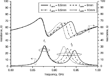
To cover the entire operating frequency range (860–960 MHz) for passive UHF RFID worldwide, Larm is taken as 9.5 mm. Figure 2.67(a) shows the simulation and measurement input impedances of the prototype antenna. The conjugate input impedance of the specified microchip is also plotted. The input resistance and reactance of the antenna vary around the conjugate value of the microchip input impedance in both f1 and f2 frequency ranges. Figure 2.67(b) shows the return loss of the antenna. The measured half-power bandwidth (RL = –3 dB) of the proposed antenna is 133 MHz (14.5%), from 842 to 975 MHz which covers the UHF RFID worldwide.
Figure 2.67. a) Measured and simulated impedance and b) return loss of the dual-band antenna with a pair of U slots for Larm = 9.5 mm
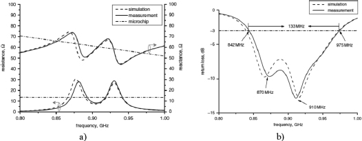
An alternative topology proposed by Rao [RAO 08] and successfully commercialized is a patch structure with an offset coplanar tapered feeding and a virtual ground short-circuit formed by the outer rectangular ring (Figure 2.68). This tag can be used to identify and track goods and articles in various production, supply chain, or asset management scenarios, including item-level applications.
Figure 2.68. Metal mount tag antenna (top layer antenna inlay)

It shows two resonant frequencies (defined by complex conjugate matching to the chip impedance) to enable the wideband performance. The overall length and width of the outer rectangular ring structure determine the lower resonant frequency while the inner radiator length determines the upper resonant frequency. The tapered trace connecting the two structures provides the complex impedance matching for RFID chip.
The flexible antenna inlay was designed so that it could be placed on top of longer dielectric piece to form a large tag with high range or wrapped around smaller piece of the same dielectric to form a small tag with less range. The antenna inlay was copper etched on 2 mil flexible polyester substrate and placed on top or wrapped around the piece of polycarbonate plastic with bottom layer of conductive material, slightly longer than the dielectric itself, as shown in Figure 2.69.
Figure 2.69. Cross-sections of a) large and b) small versions of tag

The final tag antenna and RFID chip were integrated and encapsulated inside rugged plastic packages capable of withstanding extreme temperatures and hazardous exposures, shown in Figure 2.70. The antenna design was slightly modified to take into account the influence of the plastic package. The large tag dimensions are 15.5 × 3.2 × 1 cm3 and the small tag dimensions are 7.9 × 3.1 × 1 cm3. Figure 2.71 presents experimental and theoretical read-range (boresight direction) in free space on plastic and metal (12 × 12 in). Separating two resonances makes this tag more wideband at the expense of range (bandwidth versus range tradeoff). If higher tag range in more narrow frequency band is desired, it can also be easily realized by bringing the resonances together.
Figure 2.70. a) Large and b) small metal mount UHF RFID tags
The two versions (large and small) of the tag are based on the same antenna inlay and deliver a global minimum read-range on metals of 25 and 10 ft accordingly. Both tags work reliably on various materials, including metal, across the worldwide UHF RFID frequency band (860–960 MHz).
Figure 2.71. Experimental and theoretical read-range (boresight direction) of large and small metal mount tags in free space on plastic and metal (4 W EIRP)
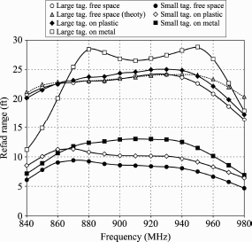
2.5.4. Improved dipole designs on metallic surfaces
In the work described in [KOO 11], there are two primary considerations that improve the performance of the antenna on metallic objects. First, in order to increase the gain on metallic objects, an additional loop surrounds the meandered folded dipole antenna. Next, to improve matching characteristics, conjugate matching of the proposed antenna is performed in the minimum impedance variation area for the metallic object so that the change of the input impedance is small compared to free space case.
Figure 2.72(a) shows the proposed folded dipole antenna #1, which is designed without consideration for metallic objects. The antenna #1 is realized with silver paste printed on a thin flexible PET substrate with a thickness of 0.07 mm. The size for the entire substrate is 82 × 18 mm2, and the line width is 1 mm.
Figure 2.72. Geometry of proposed antenna: a) antenna #1 and b) antenna #2

The proposed method to increase antenna gain is to use a multiple folded dipole configuration [POL 07]. This purpose of technique is that antenna efficiency can be improved by increasing the radiation resistance caused by the addition of the number of folded arms. Therefore, in order to increase antenna gain on the metallic object, an additional loop, which has a 2.5 mm line width, has been placed to surround the original meandered folded dipole antenna with 1 mm line width as shown in Figure 2.72(b). To validate the effect of this additional loop, two antennas are simulated as a function of distance from the metallic surface at 910 MHz and are summarized in Table 2.6. A foam spacer (εr = 1) is used for adjusting the separation from the metallic surface. Both tags are backed by a 200 × 200 mm metallic surface. As seen from Table 2.6, the peak gain of antenna #2 is higher than antenna #1 in free space as well as on the metal surface. The size of antenna #2 is 91 × 27 mm2.
Table 2.6. Simulated results of peak gain depending on distance from the metallic surface at 910 MHz
| Distance (mm) |
Antenna #1 (dBi) |
Antenna #2 (dBi) |
| 1 | –13.3 | –11.2 |
| 2 | –10.3 | –4.6 |
| 3 | –7.4 | –2.5 |
| Free space | 0.2 | 1.75 |
When the RFID tag is placed near the metallic object, the resonance moves to a lower frequency region, and then the input impedance undergoes significant frequency variation. Therefore, this change of the input impedance causes the mismatch between the chip and the antenna; so the antenna cannot deliver maximum power to the chip. To enhance the performance of RFID tags on a metallic surface, the effects of the separation from the metallic surface have been studied. Figure 2.73 illustrates the simulated impedance of the proposed antenna #2 as a function of distance between the antenna and metallic surface, and compared to the free-space case. Also, measured impedances of the IC (Alien Higgs2 in strap package) are plotted for the conjugate matching characteristic.
The IC input impedance is (7.4 – j113) Ω at 910 MHz. To deliver maximum power between the IC and the antenna, the input impedance of the antenna needs to be (7.4 + j113) Ω at 910 MHz. In free space, antenna #2 has an input impedance of (6 + j110) Ω at 910 MHz, providing a good impedance matching to the IC input impedance. However, when antenna #2 is placed on a metallic object, significant mismatch occurs in the operating frequency band 908.5–914 MHz. As can be seen from Figure 2.73, there are large variations in the input impedance depending on the distance between the metallic surface and the antenna in the frequency region B. However, there is a relatively small variation in region A. In other words, region A shows much less impedance variation on a metallic object. Thus, if conjugate matching is performed in this region, the effect of mismatch can be minimized when it is placed on a metallic object. Therefore, in order to operate antenna #2 in region A, the resonance of antenna #2 is moved to a high frequency by reducing the entire electrical length of the antenna such that the input impedance at 910 MHz is in region A.
By adjusting the T-match, the conjugate matching between the IC and the antenna is optimized at 910 MHz in free space. The overall size of the antenna is 81 × 27 mm. The experimental results show that the maximum read-range of the proposed antenna is about 7.5 m in free space, and 3 m for a 1 mm separation from the metallic surface. It is interesting to note that the read-range for 10 mm separation is 7.32 m, which is similar to that of free space.
In addition, the proposed antenna is compared to a commercial RFID label-typed tag (Alien M-Tag) also equipped with the Alien Higgs 2 chip and fabricated out of copper. Also, the overall size of the commercial tag is similar to the proposed antenna. Figure 2.74 shows a comparison between the commercial RFID label-typed tag and the proposed antenna below 5 mm separation. The proposed antenna reveals a much longer read-range than the commercial RFID antenna. For example, the read-range of the proposed antenna is about three times longer than that of the Alien M-tag when it is placed 1 mm away from the metallic surface.
Figure 2.73. Simulated input impedance as a function of distance from the metallic surface
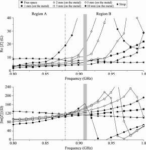
Figure 2.74. Read-range comparison against the commercial RFID tag
2.6. Bibliography
[BAL 05] BALANIS C.A., Antenna Theory: Analysis and Design, 3rd ed., John Wiley & Sons, 2005.
[BES 05] BEST R., “Low Q electrically small linear and elliptical polarized spherical dipole antennas,” IEEE Transactions on Antennas and Propagation, vol. 53, no. 3, pp. 1047–1053, March 2005.
[CHO 08] CHO C., CHOO H., PARK I., “Design of planar RFID tag antenna for metallic objects”, Electronics Letters, vol. 44, pp. 175–177, 2008.
[CHO 07] CHO C., KIM D., CHOO H., et al., “Effect of the substrate, metal-line and surface material on the performance of RFID tag antenna”, IEEE Antennas and Propagation Society International Symposium, pp. 1761–1764, 9–15 June 2007.
[DEA 09] DEAVOURS D.D., “Analysis and design of wideband passive UHF RFID tags using a circuit model”, IEEE RFID Conference, Orlando, FL, April 2009.
[DEA 10] DEAVOURS D., “UHF RFID Antennas”, RFID Systems: Research Trends and Challenges, Chapter 3, John Wiley & Sons, 2010.
[DOB 07] DOBKIN D.M., The RF in RFID: Passive UHF RFID in Practice Burlington, Newnes, 2007.
[DOB 12] DOBKIN D.M., The RF in RFID: UHF RFID in Practice, Newnes, 2012.
[DU 13] DU G.H., TANG T., DENG Y., “Dual-band metal skin UHF RFID tag antenna”, Electronics Letters, vol. 14, pp. 858–860, 4 July 2013.
[END 00] ENDO T., SUNAHARA Y., SATOH S., et al., “Resonant frequency and radiation efficiency of meander line antennas,” Electronics and Communications in Japan, Part 2 (Electronics), vol. 83, pp. 52–58, 2000.
[ERG 07] ERGEN E., AKINCI B., EAST B., et al., “Tracking components and maintenance history within a facility utilizing radio frequency identification technology”, Journal of Computing in Civil Engineering, vol. 21, no. 1, pp. 11–20, January 2007.
[GRO 04] GROVER F.W., Inductance Calculations, Dover Publications, Mineola, 2004.
[HAZ 11] HAZDRA P., CAPEK M., EICHLER J., “Radiation Q-factors of thin-wire dipole arrangements”, IEEE Antennas and Wireless Propagation Letters, vol. 10, pp. 556–560, 2011.
[HU 09] Hu Z., COLE P.H., ZHANG L., “A method for calculating the resonant frequency of meander-line dipole antenna”, Industrial Electronics and Applications (ICIEA) Conference, pp. 1783–1786, Xian, China, May 2009.
[JAC 91] JACKSON D.R., ALEXOPOULOS N.G., “Simple approximate formulas for input resistance, bandwidth, and efficiency of a resonant rectangular patch”, Transactions on Antennas and Propagation, vol. 39, no. 3, pp. 407–410, 1991.
[KIN 69] KING R.W.P., “The loop antenna for transmission and reception”, Antenna Theory, Chapter 11, McGraw-Hill, NY, p. 478, 1969.
[KOO 11] KOO T., KIM D., RYU J., et al., “Design of a label-typed UHF RFID tag antenna for metallic objects”, IEEE Antennas and Wireless Propagation Letters, vol. 10, pp. 1010–1014, 2011.
[KWO 05] KWON H., LEE B., “Compact slotted planar inverted-F RFID tag mountable on metallic objects”, Electronics Letters, vol. 44, pp. 1308–1310, 2005.
[LOP 07] LOPEZ A.R., “Wheeler and Fano impedance matching”, IEEE Antennas and Propagation Magazine, vol. 49, no. 4, pp. 116–119, 2007.
[MAR 08] MAROCCO G., “The art of UHF RFID antenna design: impedance matching and size-reduction techniques”, IEEE Antennas and Propagation Magazine, vol. 50, no. 1, pp. 66–79, February 2008.
[MCL 96] MCLEAN J.S., “A re-examination of the fundamental limits on the radiation Q of electrically small antennas”, IEEE Transactions on Antennas and Propagation, vol. 44, no. 5, pp. 672–676, May 1996.
[MCD 12] MCDONALD K.T., Reactance of small antennas, Joseph Henry Laboratories, Princeton University, Princeton, NJ, 2012.
[MO 08] MO L., ZHANG H., ZHOU H., “Broadband UHF RFID tag antenna with a pair of U slots mountable on metallic objects”, Electronics Letters, vol. 44, no. 20, pp. 1173–1174, 25 September 2008.
[NIK 05a] NIKITIN P.V., RAO K.V.S., LAM S.F., et al., “Theory power reflection coefficient analysis for complex impedances in RFID tag design”, IEEE Transactions on Microwave Theory and Techniques, vol. MTT-53, no. 5, pp. 2721–2724, September 2005.
[NIK 05b] NIKITIN P.V., LAM S., RAO K.V.S., “Low cost silver ink RFID tag antennas”, IEEE Antenna and Propagation Society International Symposium, vol. 2B, pp. 353–356, July 2005.
[OCO 09] O’CONNOR M.C., “Voyantic helps companies put RFID tags to the test”, RFID Journal, June 18, 2009. Available at: http://www.rfidjournal.com/article/view/4983.
[POL 07] POLIVKA M., AMBEMOU E., “Electrically shortened wire RFID antennas closely spaced to a PEC,” Proceedings of the 2nd European Conference on Antennas and Propagation, pp. 1–5, November 2007.
[RAO 05] RAO K.V.S., NIKITIN P.V., LAM S., “Antenna design for UHF RFID tags: a review and a practical application”, IEEE Transactions on Antennas and Propagation, vol. 53, no. 12, pp. 3870–3876, December 2005.
[RAO 08] RAO K.V.S., LAM S.F., NIKITIN P.V., “Wideband metal mount UHF RFID tag”, Proceedings of Antennas and Propagation Society International Symposium 2008, San Diego, CA, pp. 1–4, 5–11 July 2008.
[SAB 12] SABA R., DELERUYELLE T., ALARCON J., et al., “A resistant textile tag antenna for RFID UHF frequency band”, IEEE Conference on RFID Technology and Applications, Nice, France, pp. 203–207, 5–7 November 2012.
[STU 12] STUTZMAN W.L., THIELE G.A., Antenna Theory and Design, 3rd ed., Wiley, June 2012.
[SON 05] SON H.-W., PYO C.-S., “Design of RFID tag antennas using an inductively coupled feed”, Electronics Letters, vol. 41, no. 18, p. 2, September 2005.
[TAI 07] TAI C.-T., LONG S.A., “Dipoles and monopoles”, in Antenna Engineering Handbook, 4th ed., JOHN L. VOLAKIS, ed., McGraw Hill, 2007.
[UKK 05] UKKONEN L., SYDANHEIMO L., KIVIKOSKI M., “Effects of metallic plate size on the performance of microstrip patch-type tag antennas for passive RFID”, IEEE Antennas and Wireless Propagation Letters, vol. 4, pp. 410–413, 2005.
[VOL 07] VOLAKIS J., Antenna Engineering Handbook, 4th ed., McGraw-Hill, 2007.
[XI 11] XI J., YE T., “Wideband and material-insensitive RFID tag antenna design utilizing double-tuning technique”, International Symposium on Antennas and Propagation (APSURSI), Spokane, Washington, DC, pp. 545–548, 3–8, July 2011.
[XI 13] XI J., YE T.T., “Ultra low-profile metal tag antenna design with an emphasis on radiation efficiency”, 2013 IEEE International Conference on RFID (RFID ‘13), Orlando, FL, pp. 42–49, 30 April–02 May 2013.
[YAG 05] YAGHJIAN A.D., BEST S.R., “Impedance, bandwidth and Q of antenna”, IEEE Transactions on Antennas Propagation, vol. 53, no. 4, pp. 1298–1324, April 2005.