
1
Design and Performances of UHF Tag Integrated Circuits
Design of UHF RFID tag IC presents unique design challenges to satisfy constraints due mostly to the remote biaising of the batteryless tag. After a brief introduction (section 1.1) and a presentation of the architecture (section 1.2) of a tag IC, section 1.3 will show the principles of converting RF into DC via voltage multipliers successively; first in the ideal then in the real case. The end of the section will deal with the influence of the active element (the diode or the MOSFET, a comparison between the two will highlight the pros and cons of each) and passive parasitics that must be taken into account during the dimensioning of the intermediate and the output capacitors. A simplified model of the antenna and the input of the rectifier will allow us to see the importance of matching and will lead to the computation of the Power Conversion Efficiency (PCE) of the circuit. Sections 1.4 and 1.5 propose a few up-to-date circuits with careful design to reduce the threshold voltage of the active element and improve the PCE. Sections 1.6, 1.7 and 1.8 rather briefly discuss the problem of exchanging information between the reader and the tag and the improvements on the oscillator design to reduce overall consumption. Sections 1.9 and 1.10 list the latest technologies, techniques and trends used in the digital part and lists of performances of the different teams are compared.
1.1. Introduction
The ratification of the global ultra high frequency (UHF) passive radio frequency identification (RFID) standard ISO18000-6 has stimulated the interests of many research laboratories, prompting them to carry out research and development work on the UHF power rectifiers at the microwatt level. In fact, micropower rectifiers are not only limited to RFID but also useful in energy-scavenging modules for remote sensor applications [TEH 09].
The design of an integrated circuit for a UHF RFID tag is not a simple task because it requires numerous constraints to be taken into account.
The primary characteristics of an RFID tag are the cost, the communication range between the tag and the reader/writer, and the transaction time associated with the system performance. To minimize the cost, the tag should be manufactured with the tag integrated circuit (IC) and the associated antenna in a simple process; we will see later that the design rules imply both parts and then each part cannot be designed independently of the other. Despite its simple passive structure, an RFID tag should provide value-added services enabling specific RFID functions, such as data writing, the storing of historical manufacturing or distribution process data, and anticollision reads to speed up the inventory search or security functions to authenticate users [NAK 07].
First, as mentioned above, we must end up with a product for which the cost, so as not to be prohibitive for the retail RFID transponder, should be targeted at being only a few cents. Because the cost of the IC is an important part of the overall cost, it implies the choice of low-cost very large-scale integration (VLSI) technologies, which do not correspond to the best choice for some problematic designs such as the design of the rectifier. Then, a tag IC designer must deal with the challenges of low supply voltage, very low consumption, high input power dynamic range and efficient antenna matching. Because the read range is set by the forward link in a passive backscattering UHF RFID system, it means that the minimum turn-on power for the RF IC chip is of prime importance among the constraints.
A few manufacturers jealously guard their secrets about the design and fabrication process. They sell commercial products with performances as good as the ones displayed by the research laboratories. Some topics such as the optimal choice of the shunt resistor that enables the control of the received power from the far-field to the near-field are not available in the current literature but are actually implanted in certain products. This chapter aims to understand the design principles of the tag integrated circuit, especially the voltage multiplier. Some performances of the power conversion efficiency are also given with respect to different technologies and circuit topologies.
1.2. Integrated circuit architecture
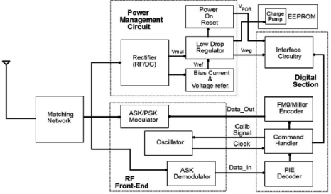
A typical block diagram of a complete passive transponder architecture, including the IC and the matched antenna, is shown in Figure 1.1. Usually, we distinguish between the front-end, which is constituted of the direct current (DC) supply generation, the demodulator and the modulator and the digital part, which includes the control logic, and the electronically erasable and programmable read-only memory (EEPROM) with its charge pump.
The transponder must draw the power required for its functioning from the received electromagnetic field. This power is used mainly by the digital section (often up to 70%) and by the front-end to receive the data sent by the reader and to allow data transmission from the tag to the reader through backscattering modulation.
The regulator circuit stabilizes the output voltage of the multiplier, but it may also keep the input voltage of the multiplier below the breakdown voltage in case of a tag being close to the base station. The voltage reference is sometimes called bandgap reference and output necessary voltages (and currents sometimes) for protection (used by regulator, for example).
1.3. RF to DC conversion: modeling the system
There are two important goals for achieving high power efficiency of the transponder. The efficiency is defined as the ratio between the RF power available at the transponder’s antenna and the DC power at the output of the DC block for supplying the transponder. The first goal is the power matching between the antenna and the IC, and the second goal is the RF to DC conversion taking into account the output load constraints, namely a minimum DC voltage to operate the transponder and a minimum load current drawn by the IC (so even if the definition mentions the output power, it is important to note [BAR 09] that each parameter must be independently satisfied). So, one of the big challenges a designer must face is the design of the rectifier with high efficiency while maintaining a minimum DC output voltage and current to supply the transponder.
Figure 1.1. Architecture of a passive RFID transponder
1.3.1. Determination of the ideal DC output voltage
For UHF RFID applications requiring several meters of communication distance, the incoming signal level is only a few hundreds of mV when minimum sensitivity is considered. Therefore, only a multistage rectifier can deal with these requirements and it is used. The topology used by Dickson in 1976 has only been slightly changed by Karthaus and Fischer [KAR 03] in order to make it useful for the alternating current (AC)/DC conversion as shown in Figure 1.3.
The received AC input voltage is converted to a DC output voltage by the voltage multiplier, which is then stabilized and maintained within limits by the voltage regulator [DEV 05].
The elementary cell is built from the clamping circuit C-D1 (see Figure 1.2(a)), which shifts the negative portion of the input signal above zero by storing the equivalent electric charge on the output terminal of C1 by the charging current circulating from ground to IN through the D1 diode. Then, the rectifier circuit detects the peak value of the output signal of the clamp circuit. The electric charge previously stored is now delivered to the output capacity Cout by the charging current circulating through D2. When considering ideal elements, we can write the voltage at the output of the clamp circuit [CUR 07]:
[1.1] ![]()
where ![]() is the peak value of Vin(t), voltage at the input of the multiplier. So, in this idealized model, the maximum possible voltage at the output of the clamp circuit is 2
is the peak value of Vin(t), voltage at the input of the multiplier. So, in this idealized model, the maximum possible voltage at the output of the clamp circuit is 2![]() . At the output of the rectifier circuit, this value is maintained by the parallel charged capacitor Cout.
. At the output of the rectifier circuit, this value is maintained by the parallel charged capacitor Cout.
In the real case, this value is reduced by the voltage drop of the diode.
[1.2] ![]()
where Vd is the diode drop voltage.
Besides, this value is further reduced due to imperfections of the circuit elements like the leakage current of the capacitor, the parasitic parallel resistor and the reverse current of the diode.
The half-wave voltage doubler is obtained by cascading the two circuits as illustrated in Figure 1.2(a).
To take advantage of both polarities of the input signal, we must use the full-wave voltage doubler as illustrated in Figure 1.2(b). This implies that the following voltage regulator is able to receive a differential input.
To reach the necessary output voltage (which depends on the complementary metal oxide semiconductor (CMOS) technology used but is actually approximately 1.2 V) when the tag is in the far-end, it is mandatory to use an N-stage multiplier, which consists of a cascade of N elementary cells.
Figure 1.2. Elementary cell of an N-stage multiplier: a) half-wave voltage doubler and b) full-wave voltage doubler

Figure 1.3. N-stage half-wave voltage multiplier and voltage regulator
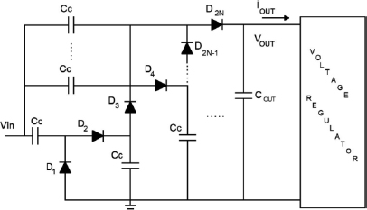
Then the voltage generated between the input and the output for an N-stage half-wave multiplier is:
In the DC analysis, capacitors act as open circuits, so we now have 2N identical diodes in series; so the voltage drop across each diode may be written with respect to time as:
[1.4] ![]()
1.3.2. Determination of the “real” DC voltage
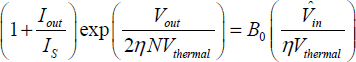
Actually, equation [1.3] is a crude approximation because the threshold voltage is considered as constant. In fact, it depends on the direct current Id and saturation current Is through an exponential law between current and voltage for the Schottky diode (or a square law in the case of a diode-connected MOS); so we have a forward diode drop that is logarithmically dependent on the diode current, which is actually the load current:
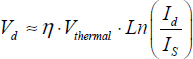
where η is the diode non-ideality factor. So, it should be rewritten as equation [1.6] to take into account this dependency but also the choice of the technology through the saturation current:
In UHF RFID applications, the amplitude of the input voltage is rather weak and the diode operates in a region where the voltage drop depends strongly on the current as shown in Figure 1.4.
Figure 1.4. Diode operational regions for Dickson’s original analysis and for UHF RFID application (after [BAR 09])

For example, if IS is 200 nA and the current through the diode varies from 2 to 4 μA, then the voltage drop will vary from 60 to 75 mV.
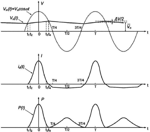
The diode current has a pulsed shape due to the nonlinear relationship (equation [1.5]) as shown by some simulations [BAR 09] in Figure 1.5 for a coupling capacitor of 1.2 pF, an output capacitor of 12 pF and a diode saturation current of 120 nA.
Figure 1.5. Voltages and currents for the Schottky diode doubler in steady-state conditions (after [BAR 09])
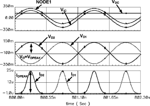
As can be seen, the threshold voltage cannot be neglected because it represents a drop approximately 100 mV (depending on the DC), which is of the same order of the amplitude of the input voltage. It is important to find the threshold voltage precisely because a small variation in it gets multiplied by the number of stages, which can significantly change the DC-generated output.
The output of the rectifier could be considered as a current source, whose value is determined by the current consumption of the IC. This means that, because of the charge conservation, the average value of the instantaneous current over one conduction cycle is equal to the load current drawn from the output, that is Iout equals 3.4 μA for this example [BAR 09]. So, if the output (or load) current increases, the peak current also increases to allow the increase of the average current as shown in equation [1.7]:

Similarly, if the input voltage increases, the peak diode current will increase as well, and thus the pulse shape will change.
So, from the viewpoint of the DC output generated, the voltage drop in the diode depends on the input voltage and the output current drawn. In fact, because of the way the rectifier works, the threshold voltage is determined only at the peak of the current ![]() .
.
So, the DC output voltage should finally be expressed by:
[1.8] ![]()
Based on the development of the relationship between current and voltage with modified Bessel function series of the exponential of a cosine function, some authors like De Vita and Iannaccone [DEV 05] establish a general N-stage rectifier input–output relationship that can be solved as:
Here, we clearly see that a designer can decide to choose Vout as the objective output parameter, leaving Iout as a dependant variable [TEH 09].
1.3.3. Effects of parasitics and capacitances on the output voltage
So far, we have only taken into account the threshold voltage as the main parameter to determine the DC output voltage but, in fact, other parameters can have a secondary influence, namely parameters of the diode model, the coupling and hold capacitors.
First, we need to know what the non-idealities are and where the parasitics for each element of the rectifier are.
1.3.3.1. Active elements parasitics
For the charge transfer devices acting as a switch, the designer has the choice between the Schottky diode, first introduced by Karthaus and Fischer in 2003 [KAR 03], and the diode-connected metal oxide semiconductor field effect transistor (MOSFET). For the latter, many alternate solutions have appeared such as the use of native transistor, special biasing circuitry, threshold programming by analog memory or the dynamic threshold MOSFET [TEH 09].
In designing a Schottky diode for a UHF RFID system, value, associated nonlinearity and the RC cutoff frequency of the diode are of primary concern. Moreover, the parasitics of the diode depend on the geometry and physical process. The way to implement diodes on a standard CMOS process must be done for an easy integration compatible with the usual masks used. Figure 1.6 illustrates a typical planar diode [JAM 06b] and its associated electrical model in Figure 1.7. It consists of a Schottky contact (Ti) to an n-well active zone and an ohmic contact to a heavily doped n+ layer. This structure allows a compact layout so as to minimize the number of extrinsic parameters and especially the capacitors.
Figure 1.6. Planar Schottky Barrier diode cross-section (after [JAM 06b])

Figure 1.7. Electrical model of the planar Schottky barrier diode cross-section(after [JAM 06b])
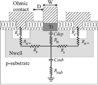
When considering the choice of the Schottky diode, it is important to have a large saturation current Is that will result in low forward voltage drop (see equation [1.5]), a small junction capacitance CD as well as small parasitic capacitance to substrate CTub. The problem is that a large Schottky diode has a large saturation current but a large capacitance also, which actually dominates the power losses, and an optimum choice of the diode has to be found.
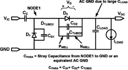
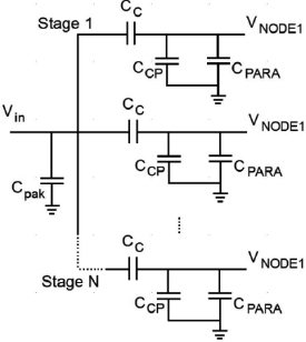
At intermediate node NODE1 in Figure 1.8, we clearly see that this substrate capacitance behaves topologically as a parallel capacitance CPARA, which is the sum of the junction capacitances CD1 and CD2 plus the “tub” capacitance of the series diode D2 labeled CTUBD2 plus the interconnect wires capacitance. CPARA is typically an order of magnitude smaller than Cc.
Figure 1.8. Schottky diode cross-section and doubler with its parasitics (after [BAR 09])
The series resistor of the diode and of the coupling capacitor can be minimized by using a multi-finger structure. Very often, the series resistor Rs is neglected in UHF RFID because the direct diode current remains low (μA), thereby inducing a low resistive drop voltage less than 1 mV.
One of the main limitations of using Schottky barrier diode (SBD) solution is the need to specially modify the CMOS process. Many laboratories have been searching for how to use the MOSFET optimally. As the size of the transistor continues to scale down, the effective threshold voltage approaches the SBD turn-on voltage [TEH 09] approximately 150–200 mV.
The difference with SBD is that the MOS actually operates in different regions in one cycle. When it is on, most of the time it is in the superthreshold region, where the drain current varies as the square of the gate-source voltage. When it is off, unfortunately, it conducts a reverse leakage current (inversion of drain and source). When the gate is connected to the source, this current is the subthreshold current and cannot be neglected because [YI 07]:
This is illustrated in Figure 1.9 where, as not shown in Figure 1.5, this reverse current induces a power dissipation.
1.3.3.2. Passive elements parasitics
In the same way, the leakage capacitance to substrate of the coupling capacitor offers a parasitic path for the charges and, consequently, it should be minimized.
Figure 1.9. Waveforms of input and output voltage, current and power dissipation (after [YI 07])
Indeed, the impact of these parasitic parallel capacitors to ground is very important. We will see later its impact in the matching issue; for now, they act as voltage dividers, as shown in Figure 1.8, and thus in the conversion equation, we must take into account not the input voltage but the modified voltage at node 1 (intermediate node).
If we consider the capacitance model as shown in Figure 1.10 [MAN 07], let us suppose that the input signal is connected to the top plate of the coupling capacitor Cc. Ahead in the model, the bonding pad and package capacitances are independent of the size of the rectifier circuit and can be grouped into Cpak. The input capacitance of the rectifier is CPARA, which has already been introduced and takes into account the parasitic capacitance to ground at the input of each stage due to the diodes or transistors. The capacitance between the bottom plate of CC and ground is CCP (typically several tens of femtofarads in design foundry manuals).
This model leads to equation [1.10], which clearly shows the effect of voltage divider depending on the values of CPARA, CC and CCP, respectively.
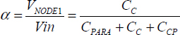
Figure 1.10. Circuit model of the parasitics of the capacitances before the ideal rectifier (after [MAN 07])
1.3.3.3. Effect of parasitics on output voltage
Equation [1.10] shows that it is very important to reduce the CPARA capacitance. Moreover, the total input capacitance clarifies the fact that all the stages are in parallel. The consequence of this parallelism is that the RF voltage applies to a much lower impedance, so we can anticipate an optimum number of stages for the multiplier with respect to the criteria of the amplitude of the input voltage.
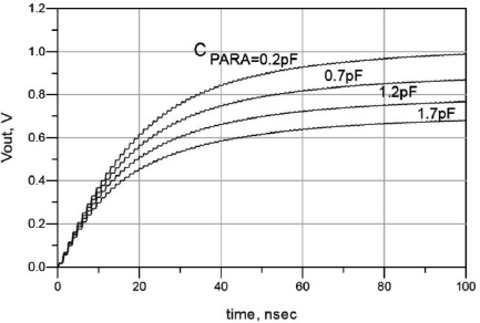
Figure 1.11 illustrates the overwhelming effect of the junction capacitance of the diode in the term CPARA that clearly demonstrates the importance of minimizing the size of the diode, irrespective of the technology used, Schottky diode or diode-connected MOS transistor.
Figure 1.11. Effect of the diode junction capacitance on the output voltage with Cc = 5 pF
1.3.3.4. Dimensioning of the intermediate capacitors
These capacitors act as charge transfer devices. They are charged during the negative cycle of the input signal and then transfer their charge to the output during the positive part of the input signal. Therefore, a small value will decrease the time to transfer the charge to the next stage. On the other hand, a large value would increase the RC time constant; the multiplier acting as a low pass filter for the input signal that can slow down the exchange of data between the reader and the tag. As a compromise and to avoid these intermediate capacitances to act as voltage dividers, it is currently admitted that these intermediate capacitors must be chosen so that they satisfy Cc ≥ 10 · CD, so typically a value approximately 2–3 pF. From equation [1.10], in this case, the loss in voltage is not more than CCP/CC.
As we have seen that the DC output power depends on the input voltage applied to the multiplier, we must consider the behavior of the circuit in the AC mode. In an AC analysis, the intermediate capacitors (all except the output capacitor) should behave as short circuits; therefore, all diodes appear in parallel to the input.
So, for these capacitors, the capacitance to substrate must be reduced. The best way to reduce it is to build them by choosing a multi-finger top metal layer configuration or making use of the capacitance between the top two metal layers [JAM 06a].
1.3.3.5. Dimensioning of the output capacitor
To ensure that the output DC voltage is constant, the output or hold capacitor C must be dimensioned so that its time constant is much larger than the period of the RF input signal [DEV 05] and thus guarantees normal operation even when the RF power from the antenna is not available for a time Tlow. If we consider that most of the load on the rectifier is due to the digital part with an on-board clock frequency Tck, then the minimum allowable value of Cout is given by [MAN 07]:
[1.11] 
where Csw is the total capacitance being switched between Vdd and ground by the digital load and α is the percentage of the Vdd drop.
This formula leads to current values approximately 50–150 pF.
1.3.3.6. Effect of parasitics on power loss
All the dynamic losses due to coupling to the substrate (see Figure 1.7) can be determined using equation [1.12] [KAR 03]:
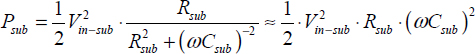
where
Vin–sub : device RF peak voltage with respect to substrate;
Csub : total capacitance to substrate;
Rsub : total series resistance to substrate.
The assumption made is valid for common low-resistivity substrate where Rsub Csubω ![]() 1.
1.
Before proceeding to the final results, we must treat the second constraint, which is the matching.
1.3.4. Matching considerations
1.3.4.1. Voltage and power at the input of the IC
The effectiveness of the power transfer between the reader and the tag can be improved by maximizing the power transfer between the tag antenna and the rectifier input structure.
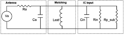
The complete system can be modeled by considering an antenna connected to the IC through a matching circuit, as shown in Figure 1.12.
Before calculating the input voltage and power at the IC terminal and deriving the input impedance of the tag, we must consider the transformation aspects brought by the matching network.
According to Barnett [BAR 09], there is no need to use a classical L-matching cell with an inductive series element because the required ratio Rin/Ra must be high to bring the Q voltage boosting at the transponder input. But, at the same time, the radiation resistance must be high to increase Va as will be demonstrated; so, series matching is not the preferred way. On the contrary, parallel inductor matching brings simplicity (same printed technology) and an improved performance to electrostatic discharge (ESD) performance. So, a simple parallel inductor easily printed at the same time as the antenna compensates for the IC input capacitance.
Figure 1.12. Simplified model of the antenna with matching and rectifier input
If we define Pav as the power available at the antenna terminal when the system antenna-rectifier is matched, we can write:
[1.13] 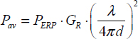
where PERP is the effective radiated power and d is the separating distance.
If Va is the antenna open-circuit voltage and Ra is the antenna radiation, then Va is related to the power available by:
[1.14] ![]()
So, we clearly see that the peak voltage Va is proportional to the square root of the radiation resistance and thus, on this criterion, we must choose an antenna with a high radiation resistance (300 Ω for a folded dipole, for example).
If we assume that the input capacitance of the IC is compensated by the parallel inductor and that the resistance Rin represents the equivalent resistance of the input resistance of the multiplier in parallel with the resistance that represents the DC consumption of the entire IC.
In this case, the voltage at the input of the IC can be written as:
[1.15] ![]()
so, maximum power Pin is absorbed by the rectifier when the antenna is matched to the rectifier, and we have Pin = Pav.
To have an idea of the voltage and power obtained in the case of the European regulations, let us make simple calculations of the resulting input power and voltage at the IC terminal in the two cases, Ra = 300Ω and Ra = 800Ω with the following parameters. Note that we do not vary the input resistance of the IC, which is often approximately 1 kΩ but decreases when the drawn DC current increases:
Table 1.1. Input power and voltage at the transponder IC
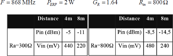
Table 1.1 clearly shows that to satisfy the two criteria of maximum power transferred and, at the same time, maximum input voltage, we must power match the antenna and the transponder IC and must have the highest antenna radiation resistance. This means that the designer needs to reduce the power consumption (choice of technology) and the input capacitance (choice of technology, number of stages and careful layout).
In these calculations, we have supposed that the backscatter modulator is removed and that only the transponder input impedance is taken into account.
As seen before, the power at the transponder antenna varies as the square of the distance between the reader and the transponder. The matching should be considered in the condition of minimum power available at the antenna to ensure correct operation of the tag, that is at largest distance (maximum operating range). Concerning the problem of deciding in which state of the input IC impedance (that is depending on the current consumption Iout) we should do this matching, the answer has been brought by Curty [CUR 07]. He showed that Rin should be considered at its minimum (output current at its maximum, so the transponder is fully functioning, both the analog and digital parts), so Vin is at its highest level when mismatch between Ra and Rin occurs.
1.3.4.2. Input equivalent impedance
In addition to the output voltage equation, an equation of the input impedance is important for optimizing the rectifier. In the aim of matching, we need to understand the physical meaning of Zin. First, we can consider two contributions to this impedance as illustrated in Figure 1.12. The impedance of the transponder includes a part that does not depend on the input voltage Vin and a part that is nonlinear and thus depends strongly on the input voltage and on the load current.
Let us first investigate the power consumption. DeVita and Iannacone considered the input power required to obtain a given output voltage and power by summing up the average power dissipated in each diode and substrate and the power required by the load Pout. Following the analysis of equation [1.9], they showed that the input power can be written as a function of a first-order modified Bessel function [DEV 05]:
[1.16] 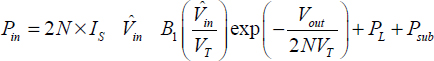
Note that the input voltage considered should be in fact Vnode1 as mentioned in equation [1.10]. So, the input resistance should be seen as an equivalent resistance linked to the power consumption:

We have seen that the relationship between the diode current and the diode voltage was nonlinear. So, here, we make an approximation, when we consider only the first term in the equivalent polynomial equation relating this absorbed current to the input voltage or input power. Even if this is far from reality because of the pulsed current (see Figure 1.5), it seems that considering resistance as the resistance that consumes a mean power Pin is enough; this approximation gives a good agreement with the measured results.
For the extraction of the equivalent input reactance, we need to know that this capacitance is a function of the voltage applied to it; so, an averaged value should be taken for a single diode as:
[1.18] 
where Vd min and Vd min are the minimum and maximum voltage drop, respectively, and the total input capacitance will be, remembering the parallelism of all diodes:
[1.19] ![]()
Then, when considering the parasitics, we can write the total capacitance at the input of the voltage multiplier:
[1.20] ![]()
where CPARA = CD1 + CD2 + CTUBD2
Actually, the resistive part must be modified because we must add the parasitics that come from the loss power in the substrate. It can be physically modeled by a series resistor Rsub (see Figure 1.7) representing a parasitic tub resistance. This circuit is converted to an equivalent parallel model [NAK 07]. So, in the end, we have an imaginary reactance due to the parasitic and diode capacitances and a real part that depends on two contributions, one of which is the current consumption and the other is due to resistive and reactive parasitics of the substrate as illustrated in Figure 1.12.
Ideally, Rp_sub should be at least 10 times the value of the antenna resistance, which is approximately 1 kΩ or less than that (but should be maximized in any case to obtain the maximum Vin). Actually, its value is dominated by the input capacitance. Furthermore, even if the input capacitance is more or less resonated by the fixed external inductor, it must be controlled because too high a capacitance means an increase of the system Q, which in turn may bring difficulty in covering the 100 MHz bandwidth around 900 MHz. For this reason, the Q is usually limited to 6–8.
EXAMPLE.–
If the operation frequency is 868 MHz and Cin is only 1 pF, then the parallel parasitic input resistance can be raised up to only 3 kΩ. At the same time, when the chip consumes 100 μA (analog and digital parts are fully functioning), the input resistance due to consumption is 10 kΩ under a DC voltage of 1 V. So, we can conclude that the required design constraint for the input impedance is to reduce the input parasitic capacitance (small diode or transistor and small substrate capacitance in the well-chosen topology).
For a commercial circuit, it is possible to find these figures: total series input resistance of 6.7 Ω, Cin = 0.88 pF, which gives a total parallel input resistance of 5.8 kΩ.
In conclusion, before showing the results obtained, we can say that a large diode (or diode-connected MOS) will show a low threshold voltage Vd and is beneficial for increasing output DC voltage given through Vout = 2N · (![]() – Vd). Also at the same time, a large diode results in large parasitic capacitance and the coupling capacitance should be increased to reduce the loss (see equation [1.10]). However, increasing Cc increases its own parasitic capacitance to ground and adds to the input capacitance of the rectifier. In fact, the diode size and the coupling capacitor should be scaled together to increase the input voltage. Further increase in voltage can be obtained by adding stages with the associated benefit of a reduction of the input resistance that eases the matching with the antenna.
– Vd). Also at the same time, a large diode results in large parasitic capacitance and the coupling capacitance should be increased to reduce the loss (see equation [1.10]). However, increasing Cc increases its own parasitic capacitance to ground and adds to the input capacitance of the rectifier. In fact, the diode size and the coupling capacitor should be scaled together to increase the input voltage. Further increase in voltage can be obtained by adding stages with the associated benefit of a reduction of the input resistance that eases the matching with the antenna.
1.3.5. Results obtained
Barnett has made an interesting approach that takes into account the previously mentioned capacitive voltage divider and highlights the importance of relating the peak diode current to the load current through a variable χ, χ = ![]() /Iout:
/Iout:
[1.21] 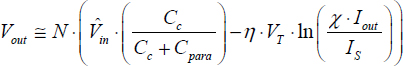
The assumption made is that the output or hold or load capacitance is much greater than the coupling capacitance, so it does not appear in the equation. This model seems to give a good matching (<5% error at maximum output current Iout) for increasing small currents with the nonlinear spice simulations, as illustrated in Figure 1.13.
Figure 1.13. Comparison between the model of equation [1.9], the nonlinear spice simulations and the model with a fixed diode drop (after [BAR 09])
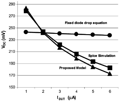
It clearly shows the strong dependence of the output voltage on the load current, more than 50% of variation for VDC for a 1–6 variation of the small load current. For strong currents (more than 20 μA), the slope decreases. So, when designing a voltage multiplier, we must take into account this fact and consider the necessary turn-on voltage as the smallest (IC is fully operating, load current approximately 80 μA).
By choosing an appropriate number of stages, any voltage can be reached. However, this can be considered valid only for a small current draw. As soon as the current increases, there is a simultaneous AC current through the capacitors, resulting in a voltage drop and a lower input voltage for the subsequent stages. In reality, there are hardly any circuits with more than 15 stages [JAM 06b].
The power conversion efficiency (PCE) is defined by the output power divided by the input power. The input power is, as seen in equation [1.17], the sum of the output power plus the losses in the diode and the loss in the substrate.
[1.22] 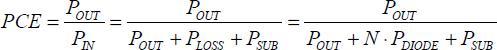
where PDIODE is the power loss of each diode: PDIODE = PFORWARD + PREVERSE
Diode losses originate from the resistive loss when current flows through the diode in the on-part of the cycle (determined by the threshold voltage) and from the reverse leakage current when the diode is in the off-part of the cycle. So, a small threshold voltage associated with a small reverse current and a small parasitic input capacitance allows us to reach high PCE.
In Figure 1.14 [KOT 09], we show the PCE as a function of input power for a large input dynamic with respect to different parameters. This study shows some comparisons with other topologies introduced in the next section like the static cancellation technique of the threshold (self-threshold-voltage cancellation (SVC) and external threshold-voltage cancellation (EVC)) and active cancellation technique (internal threshold-voltage cancellation (IVC) and the study).
It is claimed that the threshold voltage Vth can be minimized in the forward bias condition and increased in the reverse bias condition, thereby reducing the leakage reverse current.
So, in conclusion, the RF to DC equation should include the effect of the nonlinear forward voltage drop in diodes and the impedance matching conditions between antenna and rectifier input showing the important parameters for the designer, namely:
Figure 1.14. PCE and DC output voltage as a function of RF input power (after [KOT 09])

1.4. RF to DC conversion: proposed circuits and performances
1.4.1. Threshold-voltage cancellation circuit
The traditional rectifier structure based on the Dickson multiplier technology suffers from low power conversion efficiency due to the forward voltage drop in the diode or diode-connect transistor. Despite the fact that a lot of circuits implement the classical structure seen before, either with Schottky diodes or with diode-connected MOSFETs, some other solutions have been proposed. The case of using a zero-threshold transistor has not been the solution due to the significant amount of the reverse leakage current that seriously degrades the efficiency. Although process enhancement helps solve the problem but is usually insufficient, a variety of circuit design methods have attempted to achieve better performance keeping the standard process, by introducing a gate bias to reduce the effect of Vth, which is almost equal to the turn-on voltage.
Umeda [UME 06] introduced first its EVC followed by Nakamoto [NAK 07] introducing the IVC.
The rectifier proposed by Nakamoto et al. (Fujitsu) is a single-stage mirror-stacked architecture as shown in Figure 1.3; so, it differs largely from the traditional architecture where the threshold voltage is not electrically compensated. The elementary cell is shown in Figure 1.15.
In this circuit, the cancellation of the threshold voltage is achieved by inserting an internal Vth cancellation circuit (IVC) between the series PMOS Mp1 and the output VDD. Capacitor Cbp holds the threshold voltage of the PMOS diode Mp1 by replication of it with Mpb. This is done in the same way for the NMOS diode Mn2. This circuit is reported to accurately track the process and temperature variations by matching of the transistors. Rb should be chosen as being large enough to avoid the IVC branch currents.
Figure 1.16 illustrates the entire full-wave rectifier circuit. It exploits both polarities as mentioned previously to optimize power efficiency and the mirror structure contributes to eliminating the effect of the parasitic capacitances at the IN-node, which operate as the AC ground.
Figure 1.15. CMOS half-wave rectifier (after [NAK 07])

Figure 1.16. Entire full-wave rectifier with mirror stacked architecture (after [NAK 07])

The authors report a 36.6% efficiency at 953 MHz for this rectifier for an input power of −6 dBm.
1.4.2. Cross-coupled differential drive with automatic bridge structure cancellation circuit
Unfortunately with the previous circuit, when the effective threshold becomes too small due to an excessive DC bias voltage, the MOS transistor can be on for too long a time and an increased reverse leakage current appears, removing the stored charges on the output capacitor. To solve the problem, Mandal [MAN 07] and Kotani [KOT 09] brought an improvement by introducing a dynamic cancellation technique, as illustrated in Figure 1.17. They proved that it is not possible to achieve a small on-resistance and a small reverse-leakage current at the same time with static cancellation circuits.
Figure 1.17. Cross-coupled differential drive with bridge structure (after [KOT 09])

The simulation result shows a common-mode voltage (DC components of Vx and Vy) which is about half the DC output voltage is generated by the rectification operation and thus is similar to the previous schemes of static compensation. In addition to this, in this differential structure, the gate potentials depend on the differential input signal. By changing the gate polarity of MN1 (and the others of course) when Vx is either positive or negative, the resulting Ron, as well as the reverse leakage current, is reduced.
Figure 1.18 shows the measured results for the static and dynamic types of cancellation techniques, as well as the simple diode-connected transistor.
Figure 1.18. Current-voltage characteristics of diode-connected n-channel MOS transistor (after [KOT 09])

DC bias for both types is set to 0.5 V as an example. As mentioned before, the on-resistance is reduced by the static case but the reverse current is increased. In the dynamic case, both are minimized. Note that the generated voltage is:
[1.23] ![]()
1.4.3. Cross-coupled differential drive with controlled tuning voltages
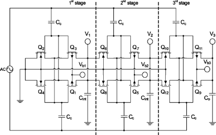
In the usual methodology, the starting point is the dimensioning of the transistors to satisfy the load current requirement. Some authors like Wong and Chen [WON 11] separate the problem of efficiency and load current by setting a set of circuit parameters (Vout, Vout/Vinpeak) and the transistor width ratio between the PFET and NFET pair). First, they find the set for maximum power conversion efficiency and, subsequently, the transistors are scaled independently in order to meet the load requirement, while keeping the set of parameters constant.
In their rectifier shown in Figure 1.19, they have chosen a cross-coupled differential drive with a bridge structure as we have seen before. All the bulk of NMOS transistors are connected to ground, whereas the bulk of PMOS transistors are differently biased according to their stage number. So, it is a different scheme from what we have just seen with the dynamic procedure where the PMOS gates were connected to the cell’s output. It has the advantages of a fine-tuning of each of these voltages according to a digital dynamic control. Note that the capacitances Cint could be omitted because the forward current of Q3 injected into the interstage is simultaneously sunk by Q8. This holds in case of perfect match between the transistors. Besides, even a small capacitance helps reducing the voltage ripple.
Figure 1.19. Three-stage differential-drive CMOS rectifier after Wong and Chen (after [WON 11])
1.4.4. Results
To illustrate the influence of the main design parameters and give an idea of the results one can obtain, we illustrate with the results given by Kotani [KOT 09] (see Figure 1.14).
An efficiency (assuming perfect matching) above 50% is obtained between −16 and –7 dBm.
The decrease of the efficiency is due to the increase of the automatic static common-mode voltage, which induces an increase of the reverse current under the large RF input conditions. Thus, it acts as a self-output power regulation system.
Concerning the dependency of PCE on frequency as illustrated in Figure 1.20, we noted that the PCE is constantly reduced when the frequency is increased. This is due to the AC resistive loss which becomes higher and the detrimental effect of the decrease of the input reactance due to Cin.
The efficiency reasonably varies with the load resistance. It changes from 90% for a 100 kΩ load corresponding to an input power of −24 dBm to a 65% for a 5 kΩ load corresponding to an input power of −9 dBm.
In a well-designed rectifier circuit, the performance should not depend strongly on the transistor size. Again, there is a compromise to make between the reduction of the on-resistance and the increase of the input capacitance leading to larger parasitic loss and leakage in the case of large transistors. On the other hand, if the transistors are too small [YI 07], then the charge transfer is incomplete, leading to a low output voltage and thus low efficiency. Hence, there must be an optimal size of transistors to maximize efficiency and output voltage.
Figure 1.20. PCE and DC as a function of Pin with frequency and output resistance as parameters (after [KOT 09])

Figure 1.21. Voltage limiter (after [FER 12])

1.5. Voltage limiter and regulator
Following the multiplier is the voltage limiter. A voltage limiter is required to avoid damages due to overvoltages whenever the tag and the reader are in close proximity.
The new architecture, which was proposed by Fernandez [FER 12], as compared with the conventional one (chain of diode-connected transistors to ground) corrects two drawbacks: first, the voltage limiter experiences less variations with respect to temperature and process dispersion. The voltage deviation is only ± 65 mV compared to ± 175 mV. To achieve that, it takes advantage of the power-on reset, bandgap reference and voltage regulator blocks. The current consumption is reported to be only 150 nA when the reader and the tag are far away, thus not degrading the sensitivity.
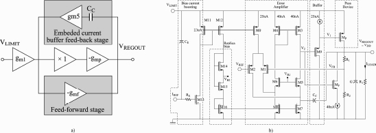
Following the voltage limiter is the voltage regulator. Due to the high modulation index used to encode the reader commands, it is not obvious to achieve a good line regulation. Besides, the power consumption of this regulator should be minimized to preserve efficiency so as to guarantee tag IC operation. One problem when designing a low-power regulator is to preserve the stability of the closed-loop system. Figure 1.22 illustrates the use of an embedded current with a feed-forward stage buffer compensation feedback stage [LEE 14] to displace the poles according to the current drawn. The circuit provides an output voltage of 1.3 V for an input coarse voltage (limited voltage) of 2.1 V and supplies a load current of 1–60 μA.
Figure 1.22. a) Block diagram of the regulator and b) schematic of the regulator(after [LEE 14])
1.6. Demodulator
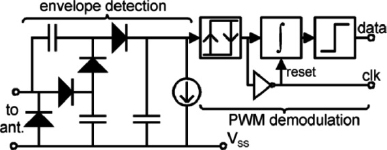
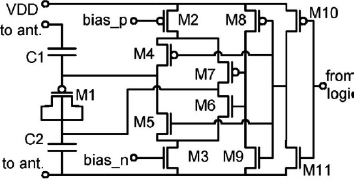
Cost prohibits the use of detection technology other than envelope detection for the amplitude modulation (ASK) or compatible schemes (DSB-ASK, SSB-ASK, PR-ASK) specified in EPC Class1Gen2 protocol. Most of the teams worldwide use the historic scheme illustrated in Figure 1.23 and proposed by the German team (Atmel) [KAR 03]. They are all based on the principle of edge detection.
So, this first block is rather similar to the circuit used in the rectifier and has the purpose of extracting the envelope of the input carrier signal. Of prime importance is the value of the capacitor of the envelope detector, together with the current sink, that should be dimensioned to extract the minimum width of gaps (approximately 4 μs) of the incoming signal. Specifications for the data envelope are given in the RFID air interface protocol. This circuit behaves as a low-pass filter that screens out the UHF carrier residue. The signal is then fed into a hysteresis comparator to generate the output data flow. The input signal to the comparator follows the input signal of the tag and displays a large dynamic range. The designer should take into account the average value of this signal to determine the hysteresis window. Then, the signal is integrated and a simple discriminator decides the length of the pulse. The integrator is used to reset by the output of the comparator inverted. This is also used as a system clock and can be reused for the internal oscillator, later used for the modulator.
Figure 1.23. Block diagram of the demodulator (after [KAR 03])
A new schematic of demodulator has been proposed by Nakamoto (Fujitsu) [NAK 07] that performs well in the case where EEPROM is replaced by ferroelectric random access memory (FeRAM) (which allows a nearly three times faster Read and Write transition time). In this case, the drawback of the conventional voltage detection scheme is that it operates in voltage mode (proportional to power) and the demodulated voltage may be reduced due to the necessary saturation curve (Vin with respect to Pin) to avoid the low device breakdown voltage of FeRAM (approximately 4 V).
The idea of obtaining a large modulated signal over the entire communication range as illustrated in Figure 1.24 is to convert the ASK input voltage into an ASK input current by maintaining the tag input voltage at a constant value. In this case, the tag input current follows the incoming power modulation linearly.
Figure 1.24. Block diagram of the current-sensing method (after [NAK 07])
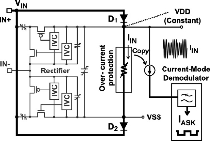
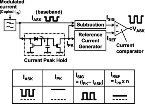
Figure 1.25 shows the block diagram of the current-mode demodulator that outputs the ASK voltage-received data. The core of it is the current comparator that compares the difference between the current-mode ASK raw data minus its peak value with a dynamic threshold, which is the peak value divided by a certain quantity approximately 10% to satisfy the minimum modulation index of 15% [NAK 07]. The authors claim a 27 dB linear dynamic range for the ASK current, corresponding to a communication range from 0 to more than 4 m.
Figure 1.25. Block diagram of the current-mode demodulator (after [NAK 07])
1.7. Oscillator
Backscattering is the principle used in RFID air interface protocol, as will be seen in Chapter 2. An RFID tag needs a clock generation circuit to output the returned data with the proper rate. A clock cannot be extracted from the input signal, which is too high in frequency (prohibitive consumption of the dividers); then, an on-board clock generator has to be designed. Fortunately, the accuracy is not a stringent constraint because protocols define relative timing rather than absolute timing; for example, EPC C1G2 uses an FM0 or Miller encoded subcarrier for the tag to reader link [ZHU 05].
When a communication is established between the tag and the reader, the latter sends a calibration signal to the tag, constituted of a series of eight pulses and each pulse being 116 μs long. At the end of this pulse, there are separation pulses that allow the tag chip to adjust its oscillation frequency as illustrated in Figure 1.26.
If each pulse received by the chip is measured with a counter clocked at 2.2 MHz, then the counted value will be 255 (116 μs × 2.2 MHz). If the frequency of the oscillator varies, the count number will vary accordingly. So, depending on the count number, each bit of successive approximation register (SAR) in the digital control block is set or reset, and the oscillation is adjusted [LEE 09].
Figure 1.26. Calibration signal from reader to tag for oscillator adjustment (after [LEE 09])

Figure 1.27 shows the schematic of a ring-type voltage-controlled oscillator (in competition with the relaxation oscillator due to its low power consumption) with digital calibration, which was proposed by Lee but introduced first by Najafi. This circuit can compensate for ±50% variation of the frequency due to process, voltage and temperature (PVT) variations with a final accuracy of less than 0.5%, satisfying the standard figure (which is less than ±15%).
Figure 1.27. Calibration signal from reader to tag for oscillator adjustment (after [LEE 09])

1.8. Modulator
In the reverse link, the most suitable modulation scheme is backscattering. Backscattering is a low-power modulation scheme in which the RFID tag reflects a part of the incident RF power back to the reader [ASH 09] by changing the input impedance of the IC.
ASK and PSK are the two modulation formats defined in the EPC Gen2 protocol. In the ASK modulation scheme, the two possible modulation states are obtained by changing a pure resistance where one state is a perfect match (Rin = Ra = and the other state is close to short circuit. In the PSK case, only the imaginary component of the switched impedance is changed whereas the resistive part is kept to match with the antenna. The classical way to implement this latter scheme is to modify the reactance of a MOSFET or varactor device. PSK is usually preferred to ASK because of its higher quality of data communication link in terms of bit error rate (BER) and constant power supply to the transponder, but ASK has the advantage of a smaller occupied area and frequency independency [MOH 06]. To illustrate this, we have chosen the phase modulator developed by Karthaus and Fischer [KAR 03].
Figure 1.28. Backscatter phase modulator (after [KAR 03])
In this circuit, the modulating reactance is achieved using an accumulation mode MOS varactor M1. The DC voltage across the varactor is varied between plus and minus VDD, thereby changing its capacitance between maximum and minimum values.
1.9. Digital blocks
In an RFID tag, less power consumption means the longer communication range. Therefore, it is essential to reduce the consumption of the digital, which corresponds to the major part of the power consumed. Usually, the static part is much lower than the dynamic power consumption. It is given by [KIM 12]:
[1.24] ![]()
where α is the switching activity (to generate all the necessary clocks), Cload is the load capacitance, VDD is the bias voltage and f is the clock frequency (usually approximately 2 MHz).
The designer should not forget the problem of the peak digital power consumption that limits reading sensitivity. Some authors [KIM 12] use adaptive techniques in order to use less power when available power is reduced.
1.9.1. Memory
Conventional tag ICs use EEPROM as the rewritable non-volatile memory (NVM). However, the typical 10 times more power required in the case of writing than reading a tag, in the case of EEPROM (charge-pump generator), has led to reduced write range, typically 80%. Researchers [NAK 07] have used FeRAM as the replacement to avoid the charge pump, enabling a nearly three times faster read-and-write transaction time.
Figure 1.29. Comparison of performances between EEPROM and FeRAM (after [NAK 07])
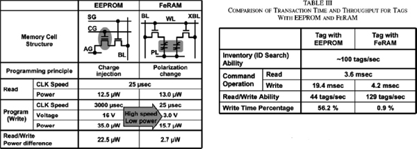
An alternative is to use an NVM [NAJ 10, KIM 12], which is compatible with a standard CMOS process and also reduces the power consumption drastically.
As illustrated in Figure 1.29, a comparison between FeRAM and EEPROM shows a consumption divided by 2 in the write mode and similar in the read mode. With NVM, another 5 to 10 factor allows drastic improvements.
1.10. Technology, performances and trends
The choice of the technology is essential in the RFID application domain. The cost objective is roughly $0.05 per chip in a small-volume production, which leaves a very small margin to develop the antenna and the bonding process, not to exceed the $0.05 tag cost goal promulgated by organizations such as EPCglobal. On the other hand, the only important technical constraint is the power consumption of the chip, because contrary to technologies used in the digital communication fields such as Wi-Fi, speed is not a real constraint in RFID applications because of the low data rate. To reach this cost by insuring the technical constraint of power consumption, the designer has to tackle different key points.
1.10.1. Technology choice
1.10.1.1. Choice in terms of rectifying device implantation
For passive UHF RFID tags, low turn-on voltage Schottky diodes or low or zero Vth diode-connected MOSFETs are typically used as rectifying devices. In microwave applications, Schottky diodes are usually fabricated in specialized processes where parameters such as barrier height, series resistance or capacitance can be fully controlled. As a result, the Schottky bulk diode (SBD) proves to be superior to the diode-connected MOSFET for the design of rectifiers.
In RFID, low cost pushes toward Schottky diode compatibility in a standard CMOS process. Several research works have been published [ZHU 05] to prove this is somewhat feasible. Due to the low series resistance, small threshold voltage and low junction capacitance, silicon–titanium Schottky diodes can be used in the rectifier.
In terms of cost, it is definitely more expensive to use Schottky diodes due to the mask process even if one reads in some articles that this is possible with no added cost.
Hence, much effort has been made to develop other CMOS solutions to overcome the SBD problem encountered by most CMOS processes. As we have seen in the proposed voltage multiplier circuits, alternate solutions proposed include the use of a programmed threshold by a bias circuitry, the use of an automatic static compensation threshold or the use of an automatic dynamic compensation threshold MOS DTMOST [TEH 09]. This is accomplished by tying the gate and the substrate together (instead of tying the body to the circuit ground). This allows the transistor to have a low leakage current when reversed biased and a high current drive (a lower threshold voltage due to the forward-bias body effect) when turned on.
A Schottky diode exhibits an exponential relationship between its current and voltage, whereas a diode-connected transistor exhibits a square law relationship. The choice of using one or the other depends on the availability of devices, cost, MOS threshold voltage variation and Schottky diode threshold variation.
When choosing the MOSFET, designers may have the choice between transistors featuring different threshold voltages. Low-threshold transistors are preferentially chosen for the front-end rectifier and high threshold transistors are for the digital core part so as to minimize the off-current leakage contribution to the power consumption. Target supply voltage can be regulated close to the transistor threshold (i.e. Vdd = 0.6 V) in order to limit the dynamic power consumption. Even lower power consumption could be reached by exploiting the subthreshold device operation. This is possible because it is enough for implementing low data rate RFID protocols. However, the main drawback in this case is the vulnerability of the circuit performance to variations in manufacturing. For instance, the turn-on voltage spread may vary considerably from one chip to the other or small fluctuations on power supply voltage would result in a large spread on critical path delays of digital circuitry [RIC 07].
A shorter MOSFET gate length should improve the performances because of the reduction in the value of the parasitics (e.g. capacitances). But actually, it is becoming less valuable to maintain the effort in trying to reduce the gate length of MOS. This is because we have reached the limits of the scalable model. For example, it is hard to consider the undergate over speed effect to model the leakage current in the ultrathin oxide layer (means a gate parasitic current).
1.10.1.2. Choice in terms of substrate choice
Preferably, the substrate should minimize the parasitic capacitances to ground. This will lower the static top plate coupling capacitance and interconnect line capacitance to ground. In this case, the substrate will be of silicon-on-insulator substrate [CUR 05]. This is more or less mandatory if one wants to work in the higher frequencies or super high frequency (SHF).
1.10.2. Design optimization
The hungry block of the analog part is the oscillator as seen before, and the architectural techniques used to reduce the power consumption of the digital block are [NAJ 10]:
At logic synthesis level, clock gating is used to reduce the switching activity of the sequential cells by removing useless edges of the clock signal, for example by limiting the operation speed of the system by the forward or reverse link data rates. Other techniques such as the gate resizing allow a significant reduction in the power consumption. Najafi reports a reduction by 10 (68 to 6 μW) by using clock gating and gate resizing (plus another technique operand isolation that does not contribute much).
1.10.3. Circuit performances
Several passive UHF RFID transponders have been published with various sensitivities; however, they often implement a simpler protocol than the one required by the EPC Gen2 specification. Implementing the complete complex protocol induces additional processing power and places a higher constraint on the transponder when we talk about sensitivity, or ultimately on maximum read/write distance. A selection of results is presented in Table 1.2 whenever the information given were more or less complete (the sensitivity is often mentioned for the Read mode but not the Write mode, which is usually more than 5 dB).
Table 1.2. Listing of performances for different design teams
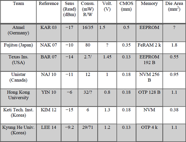
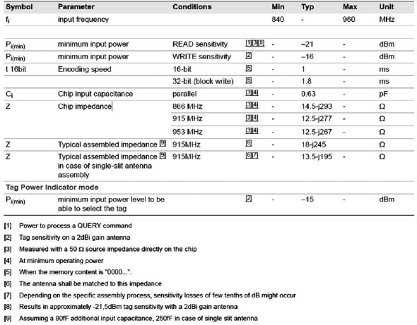
The performances of the commercially available products are largely as good as the laboratory products with the advantage of being sure that the tag fully satisfies the protocol in perfectly defined test conditions. Figure 1.30 shows the product Ucode7 proposed by NXP as an example.
Figure 1.30. Performances of the NXP product Ucode7
1.11. Bibliography
[ASH 07] ASHRY A., SHARAF K., “Ultra low power UHF RFID tag in 0.13μm CMOS”, IEEE International Conference on Microelectronics (IEEE ICM ‘07), pp. 109–126, December 2007.
[ASH 09] ASHRY A., SHARAF K., IBRAHIM M., “A compact low-power UHF RFID tag”, Microelectronics Journal, vol. 40, pp. 1504–1513, 2009.
[BAG 09] BAGHAEI M., ZOU Z., MENDOZA D.S., et al., “Remotely UHF-powered ultra wideband RFID for ubiquitous wireless identification and sensing”, in TURCU C. (ed.), Development and Implementation of RFID Technology, Open Access Database, pp. 109–126, February 2009.
[BAL 06] BALACHANDRAN G., BARNETT R., “A 110nV voltage regulator system with dynamic bandwidth boosting for RFID systems”, IEEE Journal of Solid-State Circuits, vol. 41, no. 9, pp. 2019–2028, September 2006.
[BAL 09] BALACHANDRAN G., BARNETT R., “A high dynamic range ASK demodulator for passive UHF RFID with automatic over-voltage protection and detection threshold adjustment”, IEEE Custom Integrated Circuits Conference (CICC ’09), pp. 383–386, 2009.
[BAR 06] BARNETT R., LAZAR S., LIU J., “Design of multistage rectifiers with low-cost impedance matching for passive RFID tags”, Digest IEEE Radio Frequency Integrated Circuits, pp. 291–294, June 2006.
[BAR 07] BARNETT R., BALACHANDRAN G., LAZAR S., et al., “A passive UHF RFID transponder for EPC Gen2 with -14 dBm sensitivity in 130 nm CMOS”, Digest of Technical Papers, 2007 IEEE International Solid-State Circuits Conference (ISSCC), pp. 582–583, 11–15 February 2007.
[BAR 08] BARNET R., LIU J., “An EEPROM programming controller for passive UHF RFID transponders with gated clock regulation loop and current surge control”, IEEE Journal of Solid-State Circuits, vol. 43, no. 8, pp. 1808–1815, August 2008.
[BAR 09] BARNETT R., LIU J., LAZAR S., “A RF to DC voltage conversion model for multistage rectifiers in UHF RFID transponders”, IEEE Journal of Solid-State Circuits, vol. 44, no. 2, pp. 354–370, February 2009.
[CHU 11] CHUNG C., KIM Y., KI T., et al., “Fully integrated ultra-low-passive UHF RFID transponder IC”, IEEE International Symposium on Radio-Frequency Integration Technology, Beijing, China, pp. 77–80, 30 November – 2 December 2011.
[CUR 05] CURTY J.P., JOELH N., DEHOLLAIN C., et al., “2.45 GHz remotely powered RFID system”, Proceedings of the Conference on PhD Research in Microelectronics and Electronics 2005, vol. 1, pp. 127–130, 2005.
[CUR 07] CURTY J.P., DECLERCQ M., DEHOLLAIN C., et al., Design and Optimization of Passive UHF RFID Systems, Chapters 2.1, 2.2, 2.3, 5 and 7, 1st ed., Springer, 2007.
[DOB 07] DOBKIN D.M., The RF in RFID: Passive UHF RFID in Practice, Chapter 5, Newnes, Burlington, MA, 2007.
[DON 10] DONG-SHENG L., XUE-CHENG Z., KUI D., et al., “New design of RF rectifier for passive UHF RFID transponders”, Microelectronics Journal, vol. 41, pp. 51–55, 2010.
[DU 12] DU Y., LI X., DAI L., et al., “A new type of low-power read circuit in EEPROM for UHF RFID”, Microelectronics Journal, vol. 43, pp. 364–369, 2012.
[FER 12] FERNANDEZ E., BERIAIN A., SOLAR H., et al., “A low-power voltage limiter for a full passive UHF RFID sensor on a 0.35μm CMOS process”, Microelectronics Journal, vol. 43, pp. 708–713, 2012.
[GUO 10] GUO J., SHI W., LEUNG K., et al., “Power-on-reset circuit with power-off auto-discharging path for passive RFID tag ICs”, 53rd IEEE International Midwest Symposium on Circuits and Systems (MWSCAS ’10), pp. 21–24, 2010.
[HAS 09] HASHEMI S., SAWAN M., SAVARIA Y., “A novel low-drop CMOS active rectifier for RF-powered devices: experimental results”, Microelectronics Journal, vol. 40, pp. 1547–1554, 2009.
[HON 09] HONG Y., NG Y.S., CHAN C.F., et al., “A passive RFID tag IC development platform”, 3rd International Conference on Anti-Counterfeiting, Security and Identification in Communications (ASID ’09), 2009.
[JAM 06a] JAMALI B., RANASINGHE D.C., COLE P.H., “Analysis of a UHF RFIC CMOS rectifier structure and input impedance characteristics”, Microelectronics: Design, Technology, and Packaging II, Proceedings of SPIE – the International Society for Optical Engineering, vol. 6035, 2006.
[JAM 06b] JAMALI B., RANASINGHE D.C., COLE P.H., “Design and optiisation of power rectifiers for passive RFID systems in monolithic circuit”, Microelectronics: Design, Technology, and Packaging II, Proceedings of SPIE – the International Society for Optical Engineering, vol. 6035, 2006.
[JEO 05] JEON J., “CMOS passive RFID transponder with read-only memory for low cost fabrication”, Proceedings of IEEE International SOC Conference, pp. 181–184, 2005.
[JIA 10] JIA J., LEUNG K.N., “Optimization of output voltage and stage number of UHF RFID power rectifier”, Proceedings 10th IEEE International Conference on Solid-State and Integrated Circuit Technology (ICSICT ’10), pp. 412–414, 2010.
[KAR 03] KARTHAUS U., FISCHER M., “Fully integrated passive UHF RFID transponder IC with 16.7μW minimum RF input power”, IEEE Journal of Solid-State Circuits, vol. 38, no. 10, pp. 1602–1608, October 2003.
[KIM 12] KIM Y.H., KI T.H., CHUNG C., et al., “Implementation of a low-cost and low-power batteryless transceiver SoC for UHF RFID and wireless power transfer system”, Proceedings of the 42nd European Microwave Conference, Amsterdam, pp. 514–517, 29 October–01 November 2012.
[KOT 09] KOTANI K., SASAKI A., ITO T., “High-efficiency differential-drive CMOS rectifier for UHF RFIDs”, IEEE Journal of Solid-State Circuits, vol. 44, no. 11, pp. 3011–3018, November 2009.
[LEE 09] LEE J.-W., LEE B., “A long-range UHF-band passive RFID tag IC based on high-Q design approach”, IEEE Transactions on Industrial Electronics, vol. 56, no. 7, pp. 2308–2316, July 2009.
[LEE 10] LEE K.-S., CHUN J., KWON K., “A low power CMOS compatible embedded EEPROM for passive RFID tag”, Microelectronics Journal, vol. 41, pp. 662–668, 2010.
[LEE 14] LEE J.-W., PHAN N.D., THAI Vo D.H., et al., “A fully integrated EPC-Gen2 UHF-band passive tag IC using an efficient power management technique”, IEEE Transactions on Industrial Electronics, vol. 61, no. 6, pp. 2922–2932, 2014.
[LOO 08] LOO C.H., ELMAHGOUB K., YANG F., et al., “Chip impedance matching for UHF RFID tag antenna design”, Progress in Electromagnetics Research, vol. 81, pp. 359–370, 2008.
[MAN 07] MANDAL S., SARPESHKAR R., “Low-power CMOS rectifier design for RFID applications”, IEEE Transactions on Circuits and Systems-I, vol. 54, no. 6, pp. 1177–1188, June 2007.
[MOH 06] MOHD-YASIN F., TEH Y.K., REAZ M.B.I., “Developing designs for RFID transponders”, Microwaves and RF, pp. 57–86, September 2006.
[NAJ 10] NAJAFI V., MOHAMMADI S., ROOSTAIE V., et al., “A dual-mode UHF EPC Gen2 RFID tag in 0.18μm CMOS”, Microelectronics Journal, vol. 41, pp. 458–464, 2010.
[NAK 06] NAKAMOTO H., YAMAZAKI D., YAMAMOTO T., et al., “A passive UHF RFID tag LSI with 36.6% efficiency CMOS-only rectifier and current-mode demodulator in 0.35μm FeRAM technology”, IEEE International Solid-State Circuits Conference, Digest of Technical Papers, pp. 307–310, 2006.
[NAK 07] NAKAMOTO H., YAMAZAKI D., YAMAMOTO T., et al., “A passive UHF RF identification CMOS tag IC using ferroelectric RAM in 0.35μm technology”, IEEE Journal of Solid-State Circuits, vol. 42, no. 1, pp. 101–110, January 2007.
[RIC 07] RICCI A., DE MUNARI I., “Enabling pervasive sensing with RFID: an ultra low-power digital core for UHF transponders”, Proceedings of IEEE International Symposium on Circuits and Systems, pp. 1589–1592, 2007.
[RON 06] RONGSAWAT K., THANACHAYANONT A., “Ultra low power analog front-end for UHF RFID transponder”, 2006 International Symposium on Communications and Information Technologies (ISCIT), pp. 1195–1198, 2006.
[SAS 08] SASAKI A., KOTANI K., ITO T., “Differential-drive CMOS rectifier for UHF RFIDs with 66% PCE at –12 dBm input”, Proceedings of the 2008 IEEE Asian Solid-State Circuits Conference (ASSCC ‘08), pp. 105–108, November 2008.
[SHE 13] SHEN J., WANG X., WANG B., et al., “Fully integrated passive UHF RFID transponder IC with a sensitivity of -12 dBm”, Proceedings of IEEE International Symposium on Circuits and Systems (ISCAS ’13), pp. 289–292, 2013.
[TEH 09] TEH Y.K., MOHD-YASIN F., CHOONG F., et al., “Design and analysis of UHF micropower CMOS DTMOST rectifiers”, IEEE Transactions on Circuits and Systems-II, vol. 56, no. 2, pp. 122–126, February 2009.
[UME 06] UMEDA T., YOSHIDA H., SEKINE S., et al., “A 950-MHz rectifier circuit for sensor networks tags with 10-m distance”, IEEE Journal of Solid-State Circuits, vol. 41, no. 1, pp. 35–41, January 2006.
[VIT 05] DE VITA G., IANNACONE G., “Design criteria for the RF section of UHF and microwave passive RFID transponders”, IEEE Transactions on Microwave Theory and Techniques, vol. 53, no. 9, pp. 2978–2990, September 2005.
[WON 11] WONG S.-Y., CHEN C., “Power efficient multi-stage CMOS rectifier design for UHF RFID tags”, Integration, the VLSI Journal, vol. 44, pp. 242–255, 2011.
[YAO 05] YAO Y., SHI Y., DAI F., “A novel low-power input-independent MOS AC/DC charge pump”, IEEE International Symposium on Circuits and Systems 2005, vol. 1, pp. 380–383, 23–26 May 2005.
[YI 07] YI J., KI W., TSUI C., “Analysis and design strategy of UHF micro-power CMOS rectifiers for micro-sensor and RFID applications”, IEEE Transactions on Circuits and Systems – I, vol. 54, no. 1, pp. 153–166, January 2007.
[YIN 10] YIN, J., YI J., LAW M., et al., “A system on-chip EPC Gen2 passive UHF RFID tag with embedded temperature sensor”, IEEE Journal of Solid-State Circuits, vol. 45, no. 11, pp. 2404–2420, November 2010.
[ZHA 09] ZHANG S., SUN L., HONG H., et al., “A low-power analog front end of passive UHF RFID tag IC for EPCTMC1C2”, Proceedings of 8th IEEE International Conference on ASIC (ASICON ’09), pp. 557–560, 2009.
[ZHU 04] ZHU Z., JAMALI B., COLE P., Brief comparison of different rectifier structures for RFID transponders, Report of Auto-ID Lab, University of Adelaide, 2004.
[ZHU 05] ZHU Z., JAMALI B., COLE P.H., “An HF/UHF RFID analogue front-end and analysis”, White paper series, 1st ed., Auto-ID Lab, September 2005.