
2
Review of AC Circuit Theory and Application of Phasor Diagrams
In this chapter we review the network theorems fundamental to the operation of AC circuits and the use of phasor diagrams as a tool for circuit analysis. A firm understanding of the theory and application of phasors is essential in analysing the operation of AC circuits. This chapter provides an explanation of the concepts that underpin phasor analysis as well as numerous examples of their use in analysing AC circuits. We will see that phasor analysis frequently avoids the need for complicated calculations while providing an insight into how AC circuits actually work.
We will also study the resonant behaviour of LC series and parallel circuits, and the effect that resistive losses have near resonance. We begin by considering in more detail the three‐phase system of voltage and currents.
2.1 Representation of AC Voltages and Currents
We saw in Chapter 1 that voltages in AC systems are ideally sinusoidal, and therefore they only contain energy at the system frequency ω. We also saw that three‐phase voltages are displaced from one another by 120°, like those shown in Figure 2.1.

Figure 2.1 Three‐phase 50 Hz alternating voltages (T = 20 ms).
When ![]() we see that
we see that ![]() , so we can express the ‘a’ phase voltage, va(t) as:
, so we can express the ‘a’ phase voltage, va(t) as:

where ![]() is the amplitude, ω is the angular frequency, expressed in radians per second, and T is the period of the waveform.
is the amplitude, ω is the angular frequency, expressed in radians per second, and T is the period of the waveform.
From Figure 2.1 Vb can be seen to lag Va by T/3 or 120° electrical (2π/3 radians). This is because the ‘b’ phase voltage passes through its positive going zero crossing 6.7 ms after the corresponding ‘a’ phase zero crossing.
Similarly, Vc lags Vb by 120° electrical, or alternatively we can say that Vc leads Va by the same amount. These phase voltages have an abc phase sequence, since this is the order in which they pass through zero.
We can therefore express vb(t) and vc(t) as follows:

These waveforms also are periodic, with period T, therefore we can write:
For a system frequency of 50 Hz, T = 20 ms, while for 60 Hz systems T = 16.67 ms.
We will confine our analysis to the steady state behaviour of AC circuits, where any transients arising at start‐up have long since died away. Since AC voltages are sinusoidal, so will be the AC currents flowing in circuits comprising linear components such as resistors, capacitors and inductors.
Non‐linear devices, (variable frequency drives for example), consume current at the system frequency, as well as integral multiples of it, known as harmonics. Supply authorities limit the distorting effects of harmonic currents so that system voltages generally do not contain more than about 5% total harmonic distortion. In the analysis that follows, both the voltages and the currents are assumed to be sinusoidal.
2.2 RMS Measurement of Time Varying AC Quantities
While it is relatively easy to measure the amplitude of a sinusoidal waveform (i.e. its peak value), this is not the most useful representation. Instead, engineers use a root mean square (RMS) calculation in the measurement of AC currents and voltages. The RMS concept is not restricted to sinusoids; it can be applied to any periodic time varying waveform.
The RMS value of an AC current or voltage is that which creates the same average heating effect in a resistor as a DC voltage or current of the same magnitude. Numerically, the power dissipated in an R ohm resistance by a source of DC potential VDC (= VRMS) is constant and is given by:

The average power delivered by a sinusoidal AC source to the same resistor, can be expressed as:

If these quantities are equated, we find:
The root mean square voltage can therefore be expressed as:

Thus the power delivered to an R ohm resistor by this voltage is  watts. Therefore for a sinusoidal waveform we may write:
 ![]() .
.
Similarly, RMS currents can be defined by:

The RMS value of any periodic function v(t), can be calculated using the equation:

RMS quantities are usually written in upper case, e.g. V or VRMS; they are not time varying quantities, but are constants. So as to distinguish them from the upper case notation that we will use to designate phasors, RMS values in this text will be displayed within a modulus symbol, i.e. ![]() .
.
2.3 Phasor Notation (Phasor Diagram Analysis)
All the analyses that follow are aimed at establishing the steady state response of AC circuits to sinusoidal excitation at the system frequency – that remaining after any short‐term transients have died away. Manipulating and keeping track of time varying waveforms of the kind shown in Figure 2.1 is very tedious, especially when three‐phase voltages and currents are involved. Fortunately, a shorthand notation has been developed that enables engineers to easily analyse quite complex multi‐phase circuits, known as phasor notation, or alternatively phasor diagrams. Phasor diagrams are based on the sine and cosine functions that describe alternating currents and voltages. They provide a simple and elegant visual representation of the voltages and currents that exist in AC circuits, and are applicable to Kirchhoff’s voltage and current laws, making them a very powerful tool for analysing the steady state behaviour of quite complex AC circuits.
2.3.1 Sine and Cosine as Circular Functions
Sinusoidal waveforms are strongly related to circular motion; indeed, the sine and cosine functions are often referred to as circular functions. The unit circle in Figure 2.2 can be used to define the sine and cosine functions of an arbitrary angle ϕ. If we use the positive x axis as the angular origin, then sin(ϕ) is defined as the projection of the radius on the vertical axis while cos(ϕ) is its projection onto the horizontal axis.

Figure 2.2 Definitions of sine and cosine functions.
If we allow the radius to rotate at a constant angular frequency ω, in an anticlockwise direction, commencing at t = 0 from a position on the positive x axis, then its projections onto the x and y axes describe the time varying functions cos(ωt) and sin(ωt) respectively, as illustrated in Figure 2.3.

Figure 2.3 Generation of time varying sinusoidal functions from rotary motion.
The cosine function can be seen to lead the sine, since it passes through its maximum value 90° before the sine function does. Alternatively, we can say that the sine function lags the cosine, by 90°. The shape of these functions is representative of the voltages and currents that exist in a power system.
If we consider the expressions presented above for our set of phase voltages, we see that only two quantities are required to define each one. The first is its magnitude, expressed in volts RMS, and the second is the phase angle ϕ that it takes when t = 0. For example, the ‘b’ phase voltage in the example above has an RMS magnitude of ![]() and a phase angle of
and a phase angle of ![]() radians, while the ‘c’ phase voltage has the same magnitude and a phase angle of
radians, while the ‘c’ phase voltage has the same magnitude and a phase angle of ![]() radians.
radians.
Let us now consider our circle to be drawn on the complex plane. Euler’s formula states that:
This expression represents a unit vector, rotating anticlockwise at ω radians per second, whose real coordinate is cos(ωt) and whose imaginary coordinate is sin(ωt). A rotating vector with an RMS amplitude of |V| can therefore be written as:
The left‐hand side of this equation is the polar form of the vector’s coordinates, while that on the right is their Cartesian form. Alternatively, we can represent an arbitrary cosine function by the Real part of ![]() , where:
, where:
and a sine function by the Imaginary part:
2.3.2 Phasor Representation
The phasor representation of an AC quantity is obtained by taking a snapshot of its rotating vector, thereby freezing its motion in time. The frozen vector is called a phasor. Its length represents the phasor’s magnitude in volts or amps RMS, and the exact point in time when its rotation is frozen can be chosen arbitrarily. This is usually determined with regard to a reference phasor, generally either a system voltage or current, which is assigned a phase angle of zero degrees.
The phasor in Figure 2.4 represents a voltage whose magnitude is 230VRMS and whose angle lags the reference position by 30°.

Figure 2.4 Phasor representation of an AC voltage.
If we describe a rotating voltage vector by ![]() and freeze its rotation in time, by putting
and freeze its rotation in time, by putting ![]() , we obtain the polar form of the phasor V, representing it. Thus:
, we obtain the polar form of the phasor V, representing it. Thus:
Since in the steady state, the frequency of all voltages and currents in a network is the same, the only parameters required to uniquely define any phasor are its magnitude and its phase, both of which are included in the phasor expression in Equation (2.1).
As an example, consider Figure 2.5, which shows a single‐phase induction motor. Because motors are partially inductive, as we shall see later in this chapter, the current they consume lags the applied voltage. In the associated phasor diagram, the applied voltage has been chosen as the reference phasor, and therefore its phase has been assigned a value of zero degrees. The motor current lags this voltage, in this case by an angle of 40°, and therefore it can be described in polar form by the phasor ![]() amps.
amps.

Figure 2.5 Single phase circuit and its phasor representation.
2.3.3 Three‐Phase Systems and Phasor Diagrams
Figure 2.6a shows the phasor representation of a three‐phase system of voltages. Here the ‘a’ phase has been chosen as the reference phasor, with an angle of zero degrees. Therefore its phase to neutral voltage lies along the positive real axis. If we assume a conventional phase sequence of abc, then ‘b’ phase voltage lags the ‘a’ phase by 120°, and the ‘c’ phase lags the ‘a’ by 240°. The neutral (or star) point lies at the origin. The phase sequence is abc because, with an anticlockwise rotation, this is the sequence in which the phasors pass through the reference position. It is also useful to note that abc, bca and cab all represent this phase sequence.

Figure 2.6 (a) Phase voltages (b) Line voltages (c) Summation of voltages Vab + Vbc.
There are only two possible phase sequences, the other being acb. Thus, if the sequence abc corresponds to an anticlockwise rotation of a machine, then the sequence acb will correspond to a clockwise shaft rotation.
Line voltages can also be represented as phasors, as shown in Figure 2.6b. Note that, in this case, there is no connection to the origin, and the angle between adjacent line voltages on the diagram is 60°, not 120°. The line voltages in Figure 2.6b together with the two associated phase voltages form an isosceles triangle. Since the included angle is 120°, the magnitude of each line voltage is √3 times that of a phase voltage.
Any voltage phasor represents a difference in potential between two points in a network. These points are often included as subscripts in the name of the phasor. For example, Figure 2.6b shows the line voltages derived from Figure 2.6a; these are labelled Vab, Vca and Vbc. In each case, the subscripts represent the phases between which each potential is measured. Thus Vab is the voltage of phase ‘a’ with respect to phase ‘b’ and therefore the arrowhead corresponds to phase ‘a’. Similarly phasor Vca represents the voltage of phase ‘c’ with respect to phase ‘a’. Therefore ![]() . Where the reference potential is the neutral terminal (0 volts), the second subscript is often omitted, thus
. Where the reference potential is the neutral terminal (0 volts), the second subscript is often omitted, thus ![]() .
.
The addition (or subtraction) of phasors is similar to that of vectors, since each has a particular magnitude and phase. Therefore a phasor can be moved about on the complex plane, so long as its magnitude and phase are preserved. Two phasors can thus be added by simply placing them end to end, while preserving the magnitude and phase of each one. For example, in Figure 2.6c we see that ![]() . The voltage Vac results from the vector addition of Vab and Vbc. Note also that the common subscript ‘b’ vanishes in the summation.
. The voltage Vac results from the vector addition of Vab and Vbc. Note also that the common subscript ‘b’ vanishes in the summation.
We can see from Figure 2.6b that when laid end to end the line voltages sum to zero, i.e. ![]() . We can also demonstrate this as follows:
. We can also demonstrate this as follows:
Therefore
We shall see that the ability to add or subtract phasors is particularly useful when applying Kirchhoff’s voltage and current laws.
Figure 2.7 shows phase currents included on a phasor diagram as well as phase voltages. In this example, each phase current lags its respective phase voltage by a small angle, typical of an industrial load. Three‐phase loads whose currents have the same magnitude and the same relative phase are said to be balanced. Sometimes, as in this case, the neutral reference is dropped from the voltage phasor nomenclature, especially in the case of phase voltages, since it is understood that these are always measured with respect to the neutral terminal.

Figure 2.7 Phasor representation of three‐phase balanced voltages and currents.
2.4 Passive Circuit Components: Resistors, Capacitors and Inductors
We will now review three linear components – resistors, capacitors and inductors – and from the equations describing their fundamental behaviour, we derive expressions for the impedance presented by each one.
2.4.1 Resistors
The simplest passive component is the resistive element, R. The voltage developed across a resistance is in direct proportion to the current flowing through it, as defined by Ohm’s law, i.e. ![]() , or in terms of RMS quantities we can write:
, or in terms of RMS quantities we can write: ![]() .
.
The current flowing in a resistor lies exactly in phase with the voltage developed across it, therefore the resistance R is a real number. Thus the voltage and current phasors VR and IR lie in the same direction when represented on a phasor diagram. The resistance of a conductor of constant cross‐section is proportional to its length and inversely proportional to its cross‐sectional area; the proportionality constant is called the resistivity and is given the symbol ρ, measured in ohm‐meters. Therefore we may write:
where R is the resistance in ohms, l is the length of the conductor in metres and A is its cross‐sectional area in m2.
The resistivity is equal to the resistance between opposite faces of a 1 metre cube of the material in question, and therefore for metals it takes on very small values. For example, the resistivity of copper is 1.68 × 10⁻⁸ ohm‐m at 20 °C, increasing approximately linearly with temperature to 2.04 × 10⁻⁸ ohm‐m at 75 °C.
The resistivity is the reciprocal of the conductivity (σ) of the material, which is related to the electric field strength E within the conductor and the resulting current density, J (A/m2) according to:
Sometimes it is more convenient to use conductances rather than resistances, where the conductance G, is the reciprocal of resistance. Conductances are measured in siemens, and are particularly convenient when resistances are connected in parallel, where they can be added, just as resistances connected in series are additive.
Current flows through a metallic conductor under the influence of a small internal electric field. For example, a copper conductor with a cross‐sectional area of 1 mm2, carrying a current of 1 amp has a current density ![]() . According to the equation above, the electric field strength E within this conductor is:
. According to the equation above, the electric field strength E within this conductor is:
Thus an electric field of less than 20 mV/m is sufficient to establish a current density as high as of one million amps per square metre! This is because copper is a particularly good conductor and it is for this reason that it is widely used in the construction of transformers, busbars and electrical cables.
Transmission and distribution losses should be kept as low as practical, and despite having resistivity values slightly higher than that of copper, steel reinforced aluminium conductors are increasingly used in transmission and distribution networks. This is due to the low density of aluminium, coupled with the relatively low coefficient of thermal expansion of the steel reinforcing, enabling greater span distances to be achieved between transmission towers. The minimum clearance below a transmission line is a critical parameter, and it varies with temperature. At high ambient temperatures, or high line loadings, thermal expansion causes an increase in the conductor length, increasing the sag, and reducing the clearance beneath the line.
2.4.2 Capacitors
A capacitor typically consists of two metallic plates, separated by an insulating medium known as a dielectric, as shown in Figure 2.8. If a DC voltage V is applied to a discharged capacitor, a transient current briefly flows, establishing a positive charge on one plate and a negative charge on the other, retarding further charge accumulation. Once the potential between the plates equals the applied voltage, no further current will flow. As a result of the accumulation of this charge, an electric field E is established between the plates, equal to V/d volts per metre, where V is the voltage applied and d is the distance between the plates, illustrated in Figure 2.9.

Figure 2.8 Capacitor construction.

Figure 2.9 Electric field distribution.
For a given plate area A and separation d, the accumulated charge is proportional to the voltage applied, according to the equation:
Where ε is the permittivity of the dielectric material between the capacitor’s plates. We define the term ![]() as the capacitance C, measured in farads (and named in honour of Michael Faraday). Therefore we can rewrite this equation in the form:
as the capacitance C, measured in farads (and named in honour of Michael Faraday). Therefore we can rewrite this equation in the form:
The permittivity ε is a measure of the degree to which a dielectric material is polarised by the presence of an electric field. If we consider a capacitor holding a constant charge, we can show that the inclusion of a dielectric material between its plates acts to reduce the magnitude of the electric field between them. This is because the dielectric materials become polarised by the external electric field. They contain polar molecules that form tiny electric dipoles when the positive and negative charges they contain are slightly separated by the action of the external field. This effect is shown in Figure 2.10.

Figure 2.10 Polarisation of the dielectric by the applied electric field.
These electric dipoles create an electric field of their own, which as shown opposes the external field that created them. This can be demonstrated numerically by rewriting Equation (2.2) in terms of the electric field strength E, between the plates:
Since q is assumed to be constant, then increasing the relative permittivity εr will result in a corresponding decrease in the electric field strength. This in turn leads to an increase in capacitance value, compared to one with an air dielectric (for which ![]() ), since
), since ![]() .
.
When the plates are separated by an air space, or by a vacuum, the permittivity takes on a value given the symbol εo = 8.85 × 10⁻¹² farads per metre (F/m). When dielectric materials such as polypropylene or polycarbonate are used, the permittivity increases. The permittivity of dielectric materials is usually expressed relative to the permittivity of free space, to which we give the symbol εo. We define the relative permittivity εr as:
where ε is the absolute permittivity of the dielectric material.
The relative permittivity εr is always greater than or equal to unity, and therefore the absolute permittivity is always greater than or equal to εo. For example, the relative permittivity of polycarbonate is 2.9 while that of polypropylene is 11.9. Both of these are used as dielectric materials in capacitor construction.
Capacitive Reactance and Impedance
Equation (2.2) can be rewritten in terms of the capacitance C, the accumulated charge q(t) and the applied voltage v(t), both of which may be considered as functions of time:
Unlike the case of DC excitation, which only results in the establishment of a static electric field between the plates, an alternating potential will result in a continuously changing electric field. This is accompanied by an alternating current required to deliver the charge necessary to establish the field. This current can be obtained by differentiating Equation (2.4):

Equation (2.5) shows that the current flowing in a capacitor is proportional to the rate of change of the voltage applied to it. Therefore we might reasonably expect larger currents to flow at higher frequencies. If we let ![]() then Equation (2.5) provides an expression for i(t):
then Equation (2.5) provides an expression for i(t):
Alternatively, the RMS current can be expressed in terms of the RMS voltage according to ![]() . The capacitive reactance, to which we give the symbol Xc, is therefore given by:
. The capacitive reactance, to which we give the symbol Xc, is therefore given by:

Thus the capacitive reactance does indeed fall as the frequency rises, consistent with our previous expectation. Examination of Equation (2.6) also shows that the current is phase shifted with respect to the capacitor voltage, leading it by 90°. If we define the capacitor’s complex impedance Zc as the ratio of its voltage and current phasors Vc and Ic, we find that:

The complex impedance Zc includes the phase information necessary to generate the observed phase shift in the capacitor current:

It is worth pointing out that although the impedance is generally a complex number, it is not a phasor, rather it is the ratio of two phasors and does not represent a sinusoidally varying quantity. Equation (2.7) suggests that if we choose the voltage as the reference phasor, then the current flowing in our capacitor lies along the positive j axis, as shown in Figure 2.11. Alternatively, we can say that the current leads the capacitor voltage by 90°.

Figure 2.11 Capacitor voltage and current phasor diagram.
Capacitive Susceptance and Admittance
When capacitors are parallel connected it is often more convenient to work in terms of capacitive susceptance rather than the capacitive reactance, since susceptances in parallel may be added. The susceptance Bc, is equal to the reciprocal of the reactance, and is measured in siemens, thus ![]() . The complex capacitive admittance to which we give the symbol Yc, contains phase information in the same way as the capacitive impedance does, since:
. The complex capacitive admittance to which we give the symbol Yc, contains phase information in the same way as the capacitive impedance does, since:
2.4.3 Inductors (Reactors)
An inductor essentially consists of a coil, within which a magnetic field is created by the action of a current flowing within it. Whereas the current flowing in a capacitor is related to the rate of change of the electric field that exists between its plates, the voltage dropped across an inductor is related to the rate of change of the magnetic field linking its windings. Inductors may be wound on an easily magnetised iron core, or they may be air‐cored. We will discuss the theory of magnetic circuits in a later chapter; for now we will simply consider the electrical properties of inductors, also known as reactors.
Faraday’s law of induction states that a time varying magnetic flux will induce an electric potential within a winding linking that flux. Numerically, this is expressed in Equation (2.8).

where v(t) is the induced potential, N is the number of turns on the winding and Φ(t) is the time varying magnetic flux linking the winding. In a linear inductor where the flux is proportional to the current flowing within its winding, we may write:

where i(t) is the current flowing within the winding and is the reluctance of the magnetic circuit. Reluctance in magnetic circuits is an analogous quantity to resistance in electric circuits. It relates to the physical construction of the magnetic circuit and the material from which it is made. We will discuss reluctance in more detail in Chapter 4.
By substituting Equation (2.9) into Equation (2.8) we find:

where L is the inductance of the winding, and is equal to ![]() henries.
henries.
Inductive Reactance and Impedance
If we represent the inductive voltage by ![]() and substitute this into Equation (2.10), we find that in the steady state the current is given by:
and substitute this into Equation (2.10), we find that in the steady state the current is given by:

By analogy with the capacitive case, the inductive reactance XL is given by the ratio of its RMS voltage to its RMS current, thus:

Equation (2.12) suggests that the inductive reactance increases with frequency and therefore, for a given excitation voltage, the current will decrease as the frequency increases. Examination of Equation (2.11) also shows that the inductor current is phase shifted with respect to its voltage, in this case lagging it by 90°. As before, we define the inductor’s complex impedance ZL as the ratio of its voltage and current phasors, VL and IL, thus we find that:

The phasor diagram for an inductor appears in Figure 2.12.

Figure 2.12 Inductor voltage and current phasor diagram.
Inductive Admittances
As in the capacitive case, when inductive elements are parallel connected, working in terms of admittances is usually more convenient. The inductive admittance YL is the reciprocal of the inductive impedance ZL, thus ![]() , where BL is the inductive susceptance:
, where BL is the inductive susceptance: ![]() and is measured in siemens.
and is measured in siemens.
2.4.4 General Impedance and Admittance Expressions
When resistive, inductive and capacitive elements all appear in series, their collective impedance Z can be expressed in rectangular form (Cartesian) as:
Similarly, when these elements appear in parallel, their collective admittance Y, is given by:
Since ![]() , in general we may write:
, in general we may write:
Therefore it is only when ![]() that
that ![]() and similarly only when
and similarly only when ![]() does
does ![]() .
.
Impedances and admittances may also be expressed in polar form:
Where
2.5 Review of Sign Conventions and Network Theorems
We now briefly review the major network theorems used in the analysis of AC circuits. We begin with a review of the sign convention used in defining AC voltages and currents.
2.5.1 Sign Convention
The application of the network theorems that follow requires that the voltage dropped across circuit elements be defined with the correct polarity in relation to the current flowing through them. Although these polarities reverse every half cycle in an AC circuit, the following sign convention defines the instantaneous polarities throughout the circuit at one point in time, in much the same way as they would be defined in a DC circuit.
The instantaneous potentials dropped across elements in an AC circuit arise as a consequence of the current flowing through them. We indicate this polarity by arrows, pointing in the opposite direction to the flow of conventional current which created them. Conventional current is defined as the flow of positive charge (as opposed to actual current which relates to the movement of negatively charged electrons within a conductor).
Generally, we can define the direction of currents within a circuit however we choose, so long as we are consistent in our application of the voltage sign convention. Should the value of a particular current be found to be negative, then in reality it flows in the opposite direction to that in which it was defined.
The polarity of voltage (or current) sources is also shown by use of arrows. The magnitude of a source is the RMS potential between or the RMS current flowing through its terminals. The arrowhead indicates the instantaneous positive terminal and therefore the direction in which conventional current will flow from the source.
This sign convention, when applied correctly, defines the polarity of currents and voltages as they are used in loop and mesh analyses. It is depicted in the simple circuit of Figure 2.13, where phasor E1 establishes current I1 and phasor E2 establishes current I2. Both these currents return to their respective sources through R3.

Figure 2.13 Sign conventions.
We review the major network theorems that find application in AC circuit analysis. Each of these applies to the instantaneous voltages and currents existing throughout a network, and therefore they also apply to the phasors representing them as well. In the analyses that follow we will use the phasor representation of currents and voltages.
2.5.2 Kirchhoff’s Voltage Law
Kirchhoff’s voltage law (KVL) states that the sum of all voltages dropped around any closed loop is equal to the sum of voltage sources contained within that loop. From the circuit in Figure 2.13a, using KVL we may write:
Figure 2.13a Example circuit.
Although in this simple example we appear to add voltage drops algebraically, in general AC analysis KVL requires that voltage drops be added vectorially, as complex numbers, thereby taking both their magnitude and phase into account.
2.5.3 Kirchhoff’s Current Law
Kirchhoff’s current law (KCL) states that the sum of the currents entering a junction is equal to the sum of those leaving it. Therefore from Figure 2.13a we may write:
Kirchhoff’s current law generally requires that currents be added vectorially, as complex numbers. In this simple example, however, since the voltage sources are in phase with each other and the impedances are resistive, then the currents will also lie in phase.
Suppose, for example, we wish to solve for I1 and I2 in Figure 2.13 using KVL and KCL then we might proceed as follows:
We can combine the equations obtained above using KVL and KCL to yield:
and
Using the values given in Figure 2.13, these simultaneous equations are satisfied if ![]() and
and ![]() .
.
2.5.4 Principle of Superposition
The principle of superposition applies to circuits containing linear components only. It states that any voltage or current in a linear circuit, containing multiple energy sources, can be evaluated from the sum of the contributions from each source when acting on its own (with all other sources set to zero).
The contribution from each source acting alone deserves further comment. Consider the circuit of Figure 2.13a where there are two voltage sources. When we consider the source E1 acting alone, we must remove the effects of the source E2, without limiting the current that may flow through this branch. Accordingly we must force E2 to zero, and replace this source by its equivalent internal impedance, which for a voltage source is zero ohms. Thus a voltage source is replaced by a short circuit. Similarly, if the network contains a current source, then when removed, no current must be permitted to flow in the branch, regardless of the potential developed across it. It must therefore be replaced with infinite impedance, i.e. an open circuit.
If we wish to solve for I1 and I2 in Figure 2.13a using the superposition theorem, we must add the contributions to I1 and I2 from both E1 and E2, thus:

where R2‖R3 represents the parallel combination of R2 and R3, i.e. ![]() .
.
2.5.5 Thévenin’s Theorem
The equivalent circuit of a linear network as seen from any pair of terminals, can be represented by a Thévenin equivalent voltage source Vth in series with the Thévenin equivalent impedance ZTh shown in Figure 2.14. The Thévenin equivalent voltage Vth is the open circuit potential between the terminals in question, i.e. that which appears with no external impedance connected.

Figure 2.14 Thévenin equivalent network.
The Thévenin equivalent impedance Zth is the impedance seen looking into the network terminals, with all voltage sources in the network replaced by short circuits, and all current sources replaced by open circuits.
If we wish to solve for I1 and I2 in Figure 2.13a using Thévenin’s theorem, we can consider the Thévenin equivalent of the circuit between nodes ‘A’ and ‘O’, with R3 removed. The Thévenin equivalent voltage source can be found using the superposition theorem, and is equal to the open circuit voltage, VAO:

and the Thévenin equivalent resistance Rth is equal to ![]() .
.
If we now connect R3 to the Thévenin equivalent circuit, we find that the current flowing through it is given by:

And therefore the voltage across R3 is equal to the voltage at point ‘A’ in Figure 2.13a with respect to that at point ‘O’, i.e. VAO.
So

and

2.5.6 Norton’s Theorem
Norton’s theorem is an alternative approach to Thévenin’s theorem. It states that the equivalent circuit of a linear network referenced to any pair of terminals in that network can be represented by a current source IN in parallel with an admittance YN, as shown in Figure 2.15.

Figure 2.15 Norton equivalent network.
The Norton equivalent current source is the short circuit current that would flow from the network terminals T1 and T2. The Norton equivalent impedance (1/Yn) is the same as the Thévenin equivalent impedance and it is found in the same way. From these definitions, we can see that the Thévenin equivalent voltage is equal to the Norton equivalent current divided by the Norton admittance Yn:
N.B. It should be stressed that both Thévenin and Norton’s theorems do not imply anything about the internal operation of the network to which they refer. They merely provide information relating to the combinations of voltages and currents that can be obtained from the terminals T1 and T2, under various loading conditions.
We can also use Norton’s theorem to find I1 and I2 in Figure 2.13a. As before, we proceed by determining the Norton equivalent circuit across R3, with R3 removed. The short circuit currents flowing from E1 and E2 are ![]() amps and
amps and ![]() amps respectively. Thus the total short circuit current available from node ‘A’, is
amps respectively. Thus the total short circuit current available from node ‘A’, is ![]() amps. As in the previous example, the Norton impedance is 0.666 ohms. From the Norton equivalent circuit the potential across R3 is given by:
amps. As in the previous example, the Norton impedance is 0.666 ohms. From the Norton equivalent circuit the potential across R3 is given by:

And therefore we again find that:

and:

2.5.7 Millman’s Theorem
Millman’s theorem is an extension of Kirchhoff’s current law, and in many applications it is so useful that we shall include it here with the other major network theorems. It can be derived from the circuit shown in Figure 2.16.

Figure 2.16 Circuit defining Millman’s theorem.
Millman’s theorem provides a method of calculating the unknown potential Vx, assuming all the other potentials and their associated admittances are known. All the potentials in Figure 2.16 are measured with respect to ground, and therefore this terminal is omitted in the phasor nomenclature. Since we know that the sum of all the currents flowing towards node x must add to zero then, by applying KCL to this node, we find:
On solving Equation (2.13) for Vx we find:

Equation (2.14) represents Millman’s theorem, and although it looks cumbersome it is surprisingly useful in determining an unknown potential, particularly in the presence of three or more voltage sources. If we wish to solve for I1 and I2 using Millman’s theorem, we must first find the potential VAO, shown in Figure 2.13a.
Thus:

Therefore:

and

2.6 AC Circuit Analysis Examples
In order to demonstrate these analytical techniques and to highlight the use of phasor diagrams as an analytical tool, we now investigate several practical applications, where phasor diagrams provide a visual picture of a circuit’s operation.
2.6.1 Example 1: Series and Parallel Circuits.
In this example, we analyse simple series and parallel connected AC circuits, including their phasor representations. In the series case, Figure 2.17a, we find that an impedance representation is convenient since impedances connected in series can be added, whereas in the parallel case (Figure 2.17b) an admittance approach is preferred, since connected parallel admittances can be added.


Figure 2.17 (a) Series circuit (b) Parallel circuit.
Beginning with the series connected circuit, the collective impedance can be evaluated as:
Since the current is common to each component, we assign it as the reference phasor (Figure 2.18). Accordingly, the voltage will be allocated the same phase angle as the circuit impedance. The current I is therefore given by:

Figure 2.18 Series LRC phasor diagram.
The voltage drop across each component can now be plotted on the phasor diagram. The resistive drop (IR), lies in phase with the current, the inductive drop (IXL), leads the current by 90° and the capacitive drop (IXC), lags the current by 90°. These voltage drops can now be added vectorially according to KVL, to yield the phasor corresponding to the applied voltage.
Note that since the capacitive drop is larger than the inductive one, the overall impedance is capacitive, and therefore the current leads the applied voltage, in this case by 47°.
In order to analyse the parallel connected circuit of Figure 2.17b, we compute the total admittance according to:
Since the voltage across the combination is common to all elements, we assign it as the reference phasor. Therefore the current must then take on the same phase as the circuit admittance. The voltage is thus given by:

Knowing the circuit voltage enables the current in each element to be found, which can be plotted on a phasor diagram and summed to yield the applied current, as shown in Figure 2.19.

Figure 2.19 Parallel LRC circuit phasor diagram.
Since the current flowing in the inductance exceeds that in the capacitance, the overall impedance is inductive, and the current lags the circuit voltage by 42°.
2.6.2 Example 2: Three‐Phase Loads
Where three‐phase balanced or near balanced loads are involved, it is unnecessary to represent all phases on a phasor diagram. Instead one phase is usually drawn, since it is representative of the other two. The circuit shown in Figure 2.20a represents one phase of a near balanced industrial load. In practice such a load might comprise motor driven machinery, water heating, air conditioning or refrigeration equipment, together with an assortment of single phase plug loads. Electrically all these can usually be represented by an inductive‐resistive combination, since industrial loads are generally partially inductive.


Figure 2.20 (a) Inductive load equivalent circuit (b) Phasor representation.
Since it is common to both components, the current will be chosen as the reference in the phasor diagram shown in Figure 2.20b.
The voltage developed across the resistive element lies in phase with the current, while that associated with the inductive element leads the current by 90°. Kirchhoff’s voltage law requires that the sum of the voltage drops around a circuit equals the applied voltage, so we may write:
In the phasor diagram of Figure 2.20b these voltages are added vectorially. The resultant voltage V, can be seen to lead the current by an angle ϕ, or alternatively the current lags the voltage by the same angle. As we shall see in the next chapter, the cosine of this angle is called the power factor of the load, and for reasons that will be explained, supply authorities prefer customers to ensure that their load operates at a high rather than a low power factor – that the load current lags the voltage by only a small angle.
2.6.3 Example 3: Power Factor Correction
The circuit of Figure 2.21 also shows an inductive load to which has been added a parallel connected capacitor, C, provided for the purpose of power factor correction. By adding a device that consumes a leading current, some of the lagging effects of an inductive industrial load can be offset, and an increase in the power factor of the combination results.

Figure 2.21 Inductive load with power factor correction.
In this circuit the total current splits into two components, one flowing in the load IL, and the other in the power factor correction capacitance, IC. Since the applied voltage is common to both branches of this circuit, it will now be used as the reference phasor.
By analogy with Example 2, the inductive current lags the applied voltage by an angle ϕL. In contrast, the capacitive current leads the applied voltage by 90°, as shown in Figure 2.22a. The total current, can be found by vector addition of these two phasors. The resultant current Itot can now be seen to lag the voltage by a smaller angle ϕ. Because the new phase angle is less than the old, the power factor has been increased and thus improved, but the circuit remains under‐compensated. Figure 2.22b depicts the same load with sufficient capacitance applied to make the total current appear resistive, (i.e. ![]() ), so with
), so with ![]() the circuit is now ideally compensated. Finally, Figure 2.22c shows the case where an excessively large capacitive compensation has been applied, and the total current now leads the applied voltage. The circuit is therefore over‐compensated.
the circuit is now ideally compensated. Finally, Figure 2.22c shows the case where an excessively large capacitive compensation has been applied, and the total current now leads the applied voltage. The circuit is therefore over‐compensated.

Figure 2.22 (a) Under‐compensated (b) Ideal compensation (c) Over‐compensated.
2.6.4 Example 4: Capacitive Voltage Rise
Whenever a capacitance is connected to an AC bus, there will usually be an accompanying rise in the bus voltage. This is generally only a few per cent, and is due to the fact that the supply impedance is at least partially inductive. We can demonstrate this effect by considering the single phase Thévenin representation of a three‐phase AC bus, as shown in Figure 2.23a. The bus impedance is represented by an inductive component X, and a resistance R, both of which are quite small, in addition to which R is generally considerably smaller than X.

Figure 2.23 (a) AC bus Thévenin equivalent circuit (b) Capacitive loading of an AC bus.
When the system is unloaded, the bus voltage Vb is equal to the source voltage E. However, when loaded, Vb and E are no longer equal, due to the potential dropped across the source impedance, ![]() . The connection of a capacitor, as shown in Figure 2.23b, results in a leading current, causing voltage drops across both R and X, depicted in the phasor diagram in Figure 2.24. Here we have assumed that X > R, which is frequently the case.
. The connection of a capacitor, as shown in Figure 2.23b, results in a leading current, causing voltage drops across both R and X, depicted in the phasor diagram in Figure 2.24. Here we have assumed that X > R, which is frequently the case.

Figure 2.24 Capacitive voltage rise. (Note: the voltage drops VR and VX have been considerably exaggerated in scale for reasons of clarity).
The voltage dropped across the source resistance R, lies in phase with the capacitive current, while that across the inductive impedance leads this current by 90°. Kirchhoff’s voltage law requires that ![]() , and an inspection of Figure 2.24 shows that as a consequence of this summation Vb has increased in magnitude when compared to E. (Remember that the Thévenin equivalent voltage E, is fixed.) In effect, the capacitive current IC creates a voltage drop across X that adds to Vb. It can also be seen that because VX and VR are in quadrature (i.e. they are 90° apart), VX has a much larger effect on the magnitude of Vb than does VR, so we may write:
, and an inspection of Figure 2.24 shows that as a consequence of this summation Vb has increased in magnitude when compared to E. (Remember that the Thévenin equivalent voltage E, is fixed.) In effect, the capacitive current IC creates a voltage drop across X that adds to Vb. It can also be seen that because VX and VR are in quadrature (i.e. they are 90° apart), VX has a much larger effect on the magnitude of Vb than does VR, so we may write:
If we represent the increase in Vb by δV, we can write:

where XC is the reactance of the connected capacitance. We can express the fractional rise in voltage (also known as the per‐unit voltage rise) as:

By way of example, suppose that the source impedance of a 6.6 kV three‐phase bus is 0.07 + j0.6 ohms per phase, and that a capacitor of 30 ohms reactance is connected between each phase and the neutral terminal. The resulting fractional increase in the bus voltage will be about 2% or 130 V.
For this reason, capacitors are often connected to MV and HV networks to provide voltage support during times of heavy demand. Equation (2.15) can also be used to show that the bus voltage will fall when loaded with an inductive impedance, XL. This can be achieved by replacing XC with ![]() to yield:
to yield:

So a 30 ohm inductive impedance connected to the same bus, will result in a fall of about 2% in the bus voltage.
2.6.5 Example 5: Phase Sequence Indicator Analysis
We now consider the design of a phase sequence indicator, which is a simple device capable of indicating the phase sequence of a three‐phase supply. There are many versions of this circuit in existence, all of which operate on the same principle. The basic circuit is shown in Figure 2.25, and consists of two resistive lamps and one capacitor, connected in a star (or wye) configuration.

Figure 2.25 Simplified phase sequence indicator.
The phase sequence indicator is connected between the line voltages of the supply in question, so no neutral connection is required. The circuit generates its own star‐point voltage Vs, one that is quite different from that of the unused neutral terminal, which represents zero volts. We will initially analyse the circuit using Millman’s theorem, and once we have a clear understanding of its operation, we will re‐analyse it using phasor analysis.
For the circuit to operate correctly we require that the magnitude of the capacitive admittance connected to the ‘a’ phase, be equal to the effective lamp resistances on the other two:
Recall that Millman’s theorem, as applied to this circuit, states that:

where Yi is the admittance associated with phase i and Va, Vb and Vc are the phase voltages. Let us assume that the phase voltages each have a magnitude of 1 volt, and therefore they can be expressed as:
Similarly, let us assign a magnitude of 1 siemen to each admittance, therefore we can write:
Substituting these values into Equation (2.14a) we find that ![]() V, as depicted in the phasor diagram of Figure 2.26. Here we see that there is a much larger potential dropped across the ‘b’ phase lamp than across the ‘c’ phase one. Therefore we expect that the ‘b’ phase lamp will burn more brightly than that on the ‘c’ phase.
V, as depicted in the phasor diagram of Figure 2.26. Here we see that there is a much larger potential dropped across the ‘b’ phase lamp than across the ‘c’ phase one. Therefore we expect that the ‘b’ phase lamp will burn more brightly than that on the ‘c’ phase.

Figure 2.26 Phase sequence indicator phasor diagram.
So how does this circuit indicate the phase sequence of the connected supply? From the foregoing, the brightest lamp is supplied from the phase following that connected to the capacitor, which in this case is the ‘a’ phase. Therefore in the example above, with an abc phase sequence, the ‘b’ phase lamp will burn the brightest. However, if we reverse the phase sequence, by swapping the incoming ‘b’ and ‘c’ phases, then the ‘c’ phase lamp will be the brightest, since it now follows the ‘a’ phase, thus indicating an acb phase sequence.
This circuit finds application in the connection of three‐phase motors, where the correct phase sequence must be provided in order to ensure the desired direction of rotation. It is also used in metering applications to ensure that the energy meter sees the correct voltage phase sequence, although this requirement is more important with induction‐disc meters than with electronic instruments.
Now that we have an understanding of how the phase sequence indicator works, let us analyse its operation using a phasor diagram. Essentially all we have to do is to locate the star‐point s to complete the diagram for the sequence indicator.
We do need a little information about the circuit, so we begin by applying KCL to the currents flowing towards the star point, s. Thus we find:
Therefore
We can rewrite this equation in the form of two equal currents, I′ and I″, where:
And
The current I′ consists of a component from each phase that can be drawn on a phasor diagram as shown in Figure 2.27. Here each of the three‐phase currents have been added vectorially to generate I′. Since all the admittance values have a magnitude of unity, then the magnitude of each current component will also be unity. Finally, since we have chosen unity voltages as well, both the current and voltage scales on the phasor diagram will be the same.

Figure 2.27 I′ phasor diagram.
As shown in Figure 2.27, the current I′ leads the ‘a’ phase voltage by 135° and has a magnitude of ![]() amps.
amps.
We can similarly construct a phasor diagram for I″, but since at this time we do not yet know the scale of this diagram or how to orient it, we will draw Vsn in the reference direction for convenience. I″ will also have three components and, as shown in Figure 2.28, it will lead Vsn, by 26.6°.

Figure 2.28 I″ phasor diagram.
Since we know the currents I′ and I″ are equal, we must rescale Figure 2.28 so that I″ also has a magnitude of ![]() amps and superimpose the two phasor diagrams, so that I″ lies on top of I′. However, this must be done in such a way that the current I″ leads Vsn, since this circuit is capacitive. The location of the star point voltage Vsn on the phasor diagram will then be revealed. This has been done in the diagram of Figure 2.29, where we again find that
amps and superimpose the two phasor diagrams, so that I″ lies on top of I′. However, this must be done in such a way that the current I″ leads Vsn, since this circuit is capacitive. The location of the star point voltage Vsn on the phasor diagram will then be revealed. This has been done in the diagram of Figure 2.29, where we again find that ![]() volts.
volts.

Figure 2.29 Overall phasor diagram.
Our phasor analysis of the phase sequence indicator is probably no simpler than using an analytical approach, but it does illustrate what can be achieved using phasor diagrams. In more complex circuits the phasor approach can save considerable calculation while providing the benefit of a visual appreciation of the circuit’s operation. The next example illustrates such a case.
2.6.6 Example 6: Induction Furnace Operation
This example concerns a low frequency induction furnace of the type used to melt and cast aluminium or zinc. It operates on the principle that molten metal within the furnace forms a shorted secondary winding on the furnace transformer (known colloquially as an inductor). Our interest in this furnace relates to the way in which a single‐phase furnace is supplied from a three‐phase transformer, in such a way that all phases are loaded equally and at unity power factor. This is achieved through the clever use of a line‐connected balancing reactor and capacitor, as shown in the furnace schematic of Figure 2.31. An arrangement of this kind is necessary because an induction furnace is too large a load to be supplied from one phase only.
Figure 2.30 shows a cutaway view of a small induction furnace. In particular, it depicts the location of the furnace transformer, the core of which is mounted horizontally beneath the crucible.

Figure 2.30 Sectional view of an induction furnace showing the arrangement of the furnace transformer. (Ref: ‘Industrial Electric Furnaces and Appliances’ Paschkis & Persson 1960).
The transformer core and its associated primary winding are enclosed within a refractory material capable of withstanding the temperature of the molten metal. Cast into this are channels through which the metal forms two shorted turns around the core. These channels form the throats of the furnace in which the current flowing rapidly heats and expands the metal. A strong thermosyphon action draws metal into the centre throat and expels it from those on either side, thereby ensuring an even temperature distribution throughout the melt, as depicted in Figure 2.30.
The power delivered to the melt depends on the dimensions of the throats and also of the resistance of the molten metal within them, as well as the leakage inductance that exists between the primary windings and the metallic secondary winding. The cooling of the transformer’s primary winding is critical, and in this case this is achieved by a fan forcing cool air around the winding. Alternatively de‐ionised water pumped through the winding may be employed instead.
Figure 2.31 is a simplified schematic diagram of the furnace. Power is supplied from an 11 kV:460 V three‐phase transformer, where the high voltage winding is delta connected, and the low voltage is star (or wye) connected. The LV windings supply the furnace’s own three‐phase star connected autotransformer, which provides a tapping range from 90 to 600 volts. The power delivered to the furnace can thus be adjusted using the on‐line tap‐changer, enabling precise temperature control of the melt.

Figure 2.31 Induction furnace schematic diagram.
The capacitors shown are of two types, each specified according to the quantity of reactive power (VC2/XC, expressed in volt‐amps‐reactive, VAr), that it consumes from a 600 volt AC source. Type ‘A’ supplies 200 kVAr @ 600 volts, and comprises 2 × 100 kVAr capacitors, while Type ‘B’, (used only for trimming purposes), supplies 87.5KVAr @ 600 volts, and comprises 1× 12.5KVAr, 1 × 25 kVAr and 1× 50 kVAr capacitor.
The furnace transformer, together with its seven type ‘A’ power factor correction (PFC) capacitors is connected between phases ‘a’ and ‘c’. Power factor correction is required due to the leakage impedance of the furnace transformer, which adds a substantial inductive element in series with the melt resistance, when seen reflected into the primary winding. The power factor correction capacitors are dimensioned so as to restore the furnace transformer’s phase angle to zero, and therefore its power factor to unity. (The type B capacitor is provided for trimming the value of the type A capacitors.) Thus the transformer, its PFC capacitance and the melt resistance, can all be replaced with a single equivalent resistive element connected between phases ‘a’ and ‘c’.
The air‐cored phase balancing reactor is cooled by de‐ionised water, pumped through hollow windings. It is rated at 355 kVAr @ 600 volts and is connected between the ‘b’ and ‘c’ phases. Finally the phase balancing capacitors are connected between phases ‘a’ and ‘b’ and consist of one type A capacitor and two type B, which are adjusted to provide a capacitive reactance exactly equal to that of the balancing reactor.
With the exception of the 355 kVAr rating of the balancing reactor, the technical data presented above is not essential to understanding the phasor analysis of this furnace. In the simplified schematic shown in Figure 2.32, the tap‐changers have been omitted and the furnace transformer and its associated PFC capacitors have been replaced with an equivalent resistor representing the melt, while the balancing reactor and capacitors are unchanged.

Figure 2.32 Simplified furnace schematic.
We will show that, as a result of these balancing components and the PFC applied to the furnace transformer, the incoming phase currents are balanced, and that each lies exactly in phase with its associated phase voltage. Therefore the power demanded by the furnace is shared equally across all three phases of the supply transformer. We will also use our phasor diagram to determine the maximum power rating of the furnace.
To do this we must plot the phase currents (Ia, Ib and Ic) on a phasor diagram and compare them with the associated phase voltages, making any adjustments necessary to the magnitude of the furnace current, to ensure that a unity power factor is achieved. We begin by plotting the furnace, the reactor and the capacitor currents alongside their associated line voltages, as shown in Figure 2.33. The furnace current therefore lies in phase with Vac, the reactor current lags Vcb by 90° and the capacitor current leads Vab by 90°.

Figure 2.33 Furnace, inductor and capacitor currents.
Next, from Figure 2.33 we write an equation for each of the three phase currents:

These phase currents are plotted on the phasor diagram in Figure 2.34, where we see that in order to achieve a unity power factor on each phase, the resistive furnace current must be √3 times as large as either the reactor or the capacitor current. Therefore the power rating of the furnace will be √3 times the VAr rating of the balancing reactor, thus: ![]() .
.

Figure 2.34 Phase current summations.
The resultant current flowing in each phase is equivalent to supplying a balanced resistive load, in which the power delivered by each phase is one third of that required by the furnace. From our phasor diagram, we see that the current flowing in each phase has the same magnitude as that in either the reactor or the capacitor, and on the maximum tap this is equal to 355 kVar/600 V = 592 A. Therefore the total power delivered by the supply transformer will be given by: ![]() as derived above.
as derived above.
Thus, through a clever connection of balancing components, the ‘single phase’ furnace load has been distributed equally across all three phases of the supply transformer. Without such a connection it would not be possible to operate this furnace, since 615 kW is too large a load to apply to one phase alone and would severely unbalance a local LV network.
As well as providing an equation for the rating of the furnace, the phasor diagram can also provide us with a good idea of just how this circuit works; this can be shown as follows. Since the furnace current If, is in phase with the line voltage Vac it lags the ‘a’ phase voltage by 30° while its inverse − If, leads the ‘c’ phase voltage by the same amount. In order to bring these line currents into phase with their respective voltages, the ‘a’ phase requires an additional capacitive current component, while the ‘c’ phase requires an inductive one.
The capacitive current is provided to the ‘a’ phase by the balancing capacitor, connected across Vab. If the magnitude of this current is equal to 1/√3 times that of the furnace current, then the resultant ‘a’ phase line current will lie in phase with the ‘a’ phase voltage, as required. Similarly, the ‘c’ phase furnace current − If, leads the ‘c’ phase voltage by 30° (Figure 2.34) and therefore an inductive current component is required to bring the ‘c’ phase current back in phase with the ‘c’ phase voltage. The reactor, connected across Vcb, will inject such a component, and if the magnitude of this current is equal to 1/√3 times that of the furnace current, then the resultant ‘c’ phase current will lie in phase with the ‘c’ phase voltage.
Finally, the ‘b’ phase line current is equal to minus the sum of the balancing capacitor and reactor currents, −(IL + IC), and this current conveniently falls in line with the ‘b’ phase voltage, as shown in Figure 2.34. Therefore through the use of a phasor diagram, we have not only been able to determine the furnace rating, but have also obtained an insight into the operation of the phase balancing circuitry.
2.7 Resonance in AC Circuits
Resonance arises as a result of the fact that the complex impedance of a capacitor and that of an inductor are of opposite sign. When connected in series and excited at the resonant frequency, the impedance of an inductor cancels that of a capacitor, leaving a connection which presents a very low impedance to the rest of the circuit and therefore the potential developed across the combination will be low. This is not to say, however, that large voltages cannot be generated within the series combination. Indeed, the current flowing through a series resonant circuit can generate very high voltages across both the inductor and the capacitor. However, because these are 180° out of phase with each other, the resultant voltage is usually very small. The circuit is said to be resonant at this frequency, since the applied voltage and the resulting current are in phase with each other. Should a series resonance of this kind occur within a power system, it is possible that the voltage across individual components may reach a level sufficient to cause damage. The likelihood of this occurring depends on the level of resistive damping present. This is quantified in a parameter known as the quality factor Q of the circuit, which is proportional to the ratio of the energy stored within the circuit to that dissipated, during a cycle.
Similarly, when an inductor and a capacitor are connected in parallel and excited at their resonant frequency, the admittance of the inductor cancels that of the capacitor, leaving a total admittance close to zero, thus the parallel combination effectively presents a very high impedance. However, although the current flowing into the parallel combination in this situation is small, there may be a large current circulating between the inductor and capacitor. Again, the likelihood of this depends upon the quality factor of the circuit concerned.
Natural resonances like these occasionally arise in power systems, usually at frequencies above the system frequency. When these occur at or near harmonic frequencies that exist in the network, the generation of destructive voltages or currents may result. This can cause the failure of one or more items of primary plant, and therefore underdamped network resonances are to be avoided, especially near active harmonics.
For example, when voltage support capacitors are introduced into MV and HV networks, care must be taken to avoid an adverse parallel resonance condition from arising between these components and the system impedance (which is usually inductive). Were such resonances to occur near an active network harmonic, large circulating currents could arise, sufficient to cause damage to equipment within the resonant current path. In order to avoid such resonances, de‐tuning reactors are usually installed in series with these capacitors to force the the parallel resonant frequency away from odd harmonic frequencies.
Another example of parallel resonance arises in the power factor correction (PFC) circuits briefly discussed above. Here the PFC capacitance is resonant or nearly so, with the inductive component of the load impedance that it is correcting. This near resonance condition generally has no adverse effects, although depending on the size of the load, large circulating currents may exist between the two. For this reason the PFC equipment should be placed as near to the offending load as possible.
Series Resonance
We consider the analysis of series resonance and parallel resonance separately, although the two connections generate very similar algebraic results. The partial cancellation of impedances in a series circuit, when operating at a frequency above resonance, is shown in the phasor diagram of Figure 2.35. Since the current flowing is common to all three components, it has been chosen as the reference phasor.


Figure 2.35 (a) Series tuned circuit (b) Phase diagram above resonance (c) Phase diagram at resonance.
In this case, we have included the small resistance R, in series with the winding, to represent the core and winding losses of the inductor. The capacitor on the other hand may be considered virtually lossless, since any tiny resistive or dielectric losses will generally be negligible compared to loss within the inductor. Since Kirchhoff’s voltage law requires that ![]() , in Figure 2.35 we see that the supply voltage V consists of a resistive component in quadrature with a residual component equal to
, in Figure 2.35 we see that the supply voltage V consists of a resistive component in quadrature with a residual component equal to ![]() . For frequencies above resonance the circuit appears inductive, since the current lags the applied voltage, while for frequencies below resonance it is capacitive, since the current leads the applied voltage.
. For frequencies above resonance the circuit appears inductive, since the current lags the applied voltage, while for frequencies below resonance it is capacitive, since the current leads the applied voltage.
Figure 2.35c shows the situation when the circuit operates exactly at its resonant frequency; here the voltage drops across L and C completely cancel, leaving only the resistive component, across which is dropped the applied voltage V. Resonance therefore occurs when ![]() , i.e. when
, i.e. when  radians/sec.
Under resonant conditions the circuit impedance becomes equal to R, the inductor’s winding resistance, and so there is usually little to limit the flow of current in the circuit. This is not to say that there is no voltage dropped across both L and C; it’s just that the voltage drops across these elements cancel in the summation. As shown in Figure 2.35c, there can be quite large voltage drops across both L and C, – frequently well above the applied voltage V – so these components must be rated appropriately. These resonant voltage drops can be shown to be equal to the quality factor Q multiplied by the applied voltage V.
2.7.1 Quality Factor ‘Q’
The quality factor is a parameter that describes how well a tuned circuit performs close to resonance. High Q circuits exhibit rapid changes in response around the resonant frequency, while in low Q circuits the response changes much more gradually. The Q of a circuit is defined as:

Therefore a high Q circuit will exhibit very low loss per cycle and, as we shall see, it will have a sharp peak in its amplitude response at resonance. The peak energy stored in the circuit can be expressed in terms of the peak current flowing î, as 1/2Lî2 and the energy lost per cycle is found by integrating the power loss i(t)2R, over a complete cycle. Thus we may write:

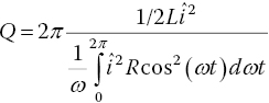


Therefore the Q of a series resonant circuit is simply the reactance of the inductor ωL, divided by its associated series resistance R, and thus a small resistive loss will give rise to a large Q value. It is interesting to note that the Q also rises with the applied frequency ω. This is because at higher frequencies a shorter cycle time is available for energy to be consumed within the resistive element. The Q of a tuned circuit is often expressed in terms of the resonant frequency of a circuit ωo, and since we have seen that for a series circuit 
 at resonance we may write:
  .
.
2.7.2 Parallel Resonance
A parallel resonant circuit can be constructed by connecting the inductor and capacitor in parallel, as shown in Figure 2.36a. Here the small resistance R still appears in series with the inductance. In this form, the parallel circuit lacks the symmetry of the series circuit, and Figure 2.36b shows a simplification of this circuit, through the introduction of a new resistive component R′, in parallel with L, in place of the resistance R in series with it. In this form, the parallel circuit is easier to analyse, although it should be stressed that this change represents an approximation to the circuit of Figure 2.36a, albeit a quite good one, especially for larger Q values.

Figure 2.36 (a) Parallel tuned circuit (b) Approximate parallel circuit
The value of the new component R′ must be chosen so that the same power loss occurs in each circuit, thus:

This means that:

And for ![]() we find:
we find:
Thus for larger Q values we can replace the series connected resistance R with an equivalent parallel resistance R ′, where ![]() .
.
2.7.3 Parallel Tuned Circuit Quality Factor
The Q value for a parallel circuit may also be expressed in terms of C and R′ from the definition in Equation (2.18):


Where ϕ is the angle between the circuit voltage and the current in the inductor:


2.7.4 Series Resonant Circuit Normalised Frequency Response
It is often useful to express the magnitude of the current flowing in a series tuned circuit I, at a frequency ω, by normalising it with respect to the current flowing at resonance Io, assuming a constant excitation potential. Therefore:


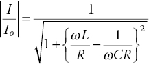


where

Equation (2.22) shows that the response at an arbitrary frequency ω, is always less than that at the resonant frequency, ωo. Figure 2.37 shows the normalised frequency response for a series resonant circuit, for various values of Q0.

Figure 2.37 Normalised frequency response of a series resonant circuit with constant excitation.
For circuits with low Q0 values, the response around the resonant frequency is not particularly sharp, but as Q0 increases so does the sharpness of the response around the resonant frequency. The maximum normalised response is unity, occurring when ω = ωo. The series resonant circuit is thus capable of passing signals near its resonant frequency, i.e. it is acting as a band‐pass filter.
2.7.5 Parallel Resonant Circuit Normalised Response
We can analyse the parallel resonant circuit’s normalised response in a similar way to the series circuit. We shall begin with the symmetrical arrangement of the three elements, L, C and R′, connected in parallel, which suggests that we approach the task from an admittance perspective, since admittances in parallel can be summed. Again we shall consider the total current flowing into the circuit from the source, and as before we shall calculate the magnitude ratio ![]() .
.
Thus:


Equation (2.23) is similar in form to Equation (2.22), but at frequencies away from resonance the value of ![]() is now considerably greater than one, since the LC combination no longer appears as an open circuit. For example, at low frequencies the inductive admittance is large, generating a high current flow. Similarly, at high frequencies the capacitive admittance is large, allowing high currents to flow. Figure 2.38 shows the normalised response plotted for several Q0 values and, as expected, as the frequency moves further from resonance, the response of the circuit increases, and as the circuit Q0 increases, so does the sharpness of the response around resonance.
is now considerably greater than one, since the LC combination no longer appears as an open circuit. For example, at low frequencies the inductive admittance is large, generating a high current flow. Similarly, at high frequencies the capacitive admittance is large, allowing high currents to flow. Figure 2.38 shows the normalised response plotted for several Q0 values and, as expected, as the frequency moves further from resonance, the response of the circuit increases, and as the circuit Q0 increases, so does the sharpness of the response around resonance.

Figure 2.38 Normalised frequency response of a parallel resonant circuit with constant excitation.
The parallel tuned circuit is capable of attenuating the signals near its resonant frequency, i.e. it is acting as a band‐stop filter.
Current Flowing in a Parallel Tuned Circuit at Resonance
Even though the total current flowing in a parallel resonant circuit is quite small, there can be a very large current circulating between the inductor and the capacitor at resonance, for which these components must be adequately rated. The magnitude of this circulating current is Q0 times the total current flowing, i.e. that in the resistive element R′. This can be easily shown as follows. The current circulating between the capacitor and the inductor is given by ![]() , and the total current flowing in the circuit at resonance Io, is given by
, and the total current flowing in the circuit at resonance Io, is given by ![]() , where V is the applied voltage. Therefore the ratio of these quantities becomes
, where V is the applied voltage. Therefore the ratio of these quantities becomes  . Thus
 ![]() . So the circulating current at resonance is Q0 times as large as the total current flowing in the parallel combination.
. So the circulating current at resonance is Q0 times as large as the total current flowing in the parallel combination.
2.7.6 Resonant Circuit Bandwidth and Cut‐Off Frequencies
The characteristic shown in Figure 2.37 is typical of a band‐pass filter, while that of Figure 2.38 is characteristic of a band‐stop filter. It is instructive to evaluate the upper and lower cut‐off frequencies for both the series and parallel resonant circuits – those frequencies at which the magnitude of the normalised response falls by 1/√2. This corresponds to a change in the power dissipated in the circuit of a factor of 2, and as a result the cut‐off frequencies are also known as the half‐power frequencies, (or alternatively as the 3 dB frequencies).
From Figure 2.35, the current in a series circuit at resonance is V/R, occurring when the reactance term X equals zero. As the frequency changes the reactance will vary as depicted in Figure 2.39. The magnitude of the normalised response will fall by a factor of 1/√2 when ![]() , occurring at the upper cut‐off frequency, or when
, occurring at the upper cut‐off frequency, or when ![]() at the lower cut‐off frequency. The upper frequency can therefore be found from the condition
at the lower cut‐off frequency. The upper frequency can therefore be found from the condition ![]() , and the lower one from
, and the lower one from ![]() . Each of these quadratic equations will yield two roots, only one of which will be positive and will represent the respective cut‐off frequency.
. Each of these quadratic equations will yield two roots, only one of which will be positive and will represent the respective cut‐off frequency.

Figure 2.39 Upper and lower cut‐off frequency definition.
The quadratic equation for the upper cut‐off frequency may be written in the form:

Which leads to the result:
Similarly, the lower cut‐off frequency is obtained from the equation:

which yields:
So for large Q values the upper and lower cut‐off frequencies lie close to the resonant frequency ωo, which is consistent with the sharp band‐pass response we have observed in such circuits. The bandwidth of the circuit (radians/sec) is defined as the range of frequencies between ωlower and ωupper which, from Equations (2.24) and (2.25), may be expressed in the form:
Equation (2.26) is often used as an alternate definition for the quality factor Q. The same analysis when applied to a parallel resonant circuit generates identical results.
2.7.7 Parallel Tuned Circuit Resonant Frequency
The analysis thus far has suggested that the effects of the inductor’s winding resistance R can be accounted for by placing a large resistance R′ in parallel with L and C (Figure 2.36). While this approximation is generally quite good, especially for high Q circuits, it fails to predict a slight downward shift in the resonant frequency of the parallel circuit when compared with that of the series circuit.
The approximate circuit suggests that the resonant frequency will be the same for both series and parallel circuits, but this is not quite correct. This assertion can be demonstrated using a phasor diagram, as shown in Figure 2.40.

Figure 2.40 Parallel tuned circuit phasor diagram.
This phasor diagram can be constructed by first choosing the inductive current as the reference phasor, i.e. lying along the positive horizontal axis. Once this current has been drawn, both the resistive and inductive voltage drops can be included (VR and VL respectively). (Remember: VL leads this current by 90°, while Vr is in phase with it.) From these phasors, the total voltage V can be found, since ![]() .
.
The capacitive current can be included next, since it leads the total voltage by 90°. Finally, the total current phasor can be constructed, since ![]() . This phasor diagram has been constructed when the circuit is operating at resonance, which occurs when the applied voltage and the resulting current are in phase. From our knowledge of AC circuit theory, we can write down equations for some of the important quantities in the circuit.
. This phasor diagram has been constructed when the circuit is operating at resonance, which occurs when the applied voltage and the resulting current are in phase. From our knowledge of AC circuit theory, we can write down equations for some of the important quantities in the circuit.
Specifically:

From the geometry of the phasor diagram at resonance we can see that:
therefore:

where ωp is the parallel resonant frequency.
Thus:


Here ωs is the series resonant frequency  and
and ![]() .
.
Therefore the parallel resonant frequency, ωp is often just a little less that the series resonant frequency, particularly when the circuit Q0 is low, say ![]()
By way of example, a 3 mH inductor with a winding resistance of 7 ohms is series resonant with a 1 μF capacitance at 2.91 kHz. When these components are connected in parallel then according to the above equation, the resonant frequency becomes 2.87 kHz. For a high Q circuits like this one the difference is not particularly great and the approximation is quite reasonable. However, for low Q circuits, the parallel resonant frequency can be significantly different. If, for example, the same inductor is resonated with 10 μF, the series resonant frequency would become 919 Hz while the parallel resonant frequency would only be 840 Hz – quite different!
2.8 Problems
- An unbalanced three‐phase load is connected to a balanced 230 V three‐phase supply, shown in Figure 2.41.
- Use Millman’s theorem to find VSN, the star point voltage in Figure 2.41. (Answer: VSN = 0 volts)
- Use your result from part (a) and further calculations to determine the Thévenin equivalent circuit between the star point and the neutral terminal. (Answer: VTh = 0 volts,
 ohms)
ohms) - Find the neutral current that would flow if the load star point and the neutral terminal were connected. The phase voltages are each 230 V. (Answer: 0 amps. Note that this does not mean that the load is necessarily balanced; it’s just that in this case the phase currents happen to sum to zero.)

Figure 2.41 Diagram for question 1. (R = 230 Ω, L = 1.267 H, C = 8 μF)
- Repeat question 1 if the inductor and capacitor are swapped, i.e. the capacitor is connected to the white phase and the inductor to the blue, as shown in Figure 2.42. (This is the equivalent of reversing the phase sequence.)
- (Answer:
 volts)
 - (Answer:
 volts, ZTh = 230 ohms)
 - (Answer: IN = 2 amps)

Figure 2.42 Diagram for question 2. (R = 230 Ω, L = 1.267 H, C = 8 μF)
- (Answer:
- Use superposition to find the neutral current that would flow if the star point ‘S’ and the neutral terminal in Figure 2.42 were connected. Draw the complete phasor diagram, showing the phase voltages and currents and their summation to produce the neutral current.
(Answer: IN = 2 amps).
- Figure 2.43 shows two possible three‐phase load connections, star and delta. If the power consumed by each load is to be the same, determine the relationship between r and R. (The average power in a resistive load R, is given by
 ).
).

Figure 2.43 Star and delta connections.
- A balanced three‐phase industrial load is represented by the single phase circuit of Figure 2.44.
- Draw the complete phasor diagram showing all the phase voltages and currents.
- Determine the phase angle ϕ between each phase voltage and its associated current. (Answer: 14° lagging)
- Show on your phasor diagram how each phase current would change if a small capacitance were connected in parallel with the load. What value of capacitive reactance would be required in order to make ϕ = 0? (Answer: 40 ohms)

Figure 2.44 Diagram for question 5. (R = 10 ohms, XL = 40 ohms)
- Show that a series L‐R circuit can be considered equivalent to a parallel L‐R circuit, as shown in the Figure 2.45, if the relationships between there quantities are as follows:


Figure 2.45 Series and parallel circuit equivalence.
- The schematic diagram shown in Figure 2.46 relates to an induction furnace having two furnace transformers (inductors). It is also designed to spread what effectively is a two‐phase load evenly over all three phases, in such a way that each sees a resistive load. Each furnace transformer is capable of delivering 550 kW to the melt when supplied with 660 V. In this circuit, no balancing reactor is employed; instead each furnace transformer is provided with a different set of power factor correction capacitors.

Figure 2.46 Two inductor furnace simplified schematic diagram.
Calculate:
- The effective melt resistance, seen looking into the primary winding of each furnace transformer. (Answer: 0.792 ohms)
- The reactive impedance that exists in parallel with the melt resistance, if the primary circuit has a power factor of 0.5.(Answer: 0.457 ohms)
- The total current flowing on the supply side of each PFC capacitor.(Answer: transformer 1: 962 A, 30° lagging, transformer 2: 962 A, 30° leading.)
- The minimum rating required for the flexible cables supplying each furnace transformer.(Answer: 1667 A)
Plot the phase currents on a phasor diagram along with the phase voltages, and hence determine the VA rating for the delta‐star connected supply transformer. (You may assume that the autotransformer is lossless.) (Answer: 1100 kVA, all phases resistively loaded.)
- The induction furnace schematic in Figure 2.31 shows that the flexible cables supplying the furnace transformer are rated at 2600 A. If the furnace transformer is modelled by an inductance L, in parallel with the equivalent furnace resistance R, and complete PFC is provided by seven type ‘A’ capacitors, calculate the current that will flow to the furnace transformer when it operates at maximum power. Compare your result to the cable rating.
(Answer: 2548 A)
- A coil with resistance of 4.5 Ω but unknown inductance is connected in series with a 0.12 μF capacitor to form a series resonant circuit. The measured centre frequency (resonant frequency) is 7.2 kHz. The same coil is now to be used in a parallel resonant circuit with a new capacitor, to be resonant at 5 kHz.
- What parallel capacitance is required?(Answer: C = 0.249 μF)
- Estimate the Q and the bandwidth of the parallel circuit.(Answer: Q = 28.4, BW = 176 Hz)
- If a bandwidth of 500 Hz is required for the parallel circuit what value of resistance would be needed:
- If an extra resistance is connected in parallel with the coil?(Answer: Rextra = 1.97 kΩ)
- If the extra resistance is connected in series with the coil?(Answer: Rextra = 8.3 Ω)
-
- A Calculate the cut‐off frequencies of the circuit in Question 9A.
- BWhat will these frequencies become when the bandwidth is increased as in 9C? (Answer a: 7.32 kHz and 7.07 kHz, b: 7.70 kHz and 6.94 kHz)
- An LC parallel resonant circuit shown in Figure 2.47 is to be used in a metal detector circuit. The inductance value is 300 μH with a winding resistance of 1.0 Ω. The circuit is to be resonant at 10 kHz and is to be excited from a 5 V, 10 kHz supply.

Figure 2.47 Parallel resonant circuit.
Find:
- The capacitance value required(Answer: 0.845 μF)
- The circuit bandwidth(Answer: 531 Hz)
- The 3 dB frequencies(Answer: 10.26 kHz, 9.73 kHz)
- The total current drawn from the supply at resonance.(Answer: 14 mA)
- The metal detector circuit described in question 11 is operated at a frequency of 9 kHz. When a non‐ferrous metal object enters the magnetic field surrounding the inductor, energy is absorbed from the field by the eddy current losses within the metal. This is reflected as an increase in the power supplied to the circuit from the 5 volt exciting voltage. If a particular metal object, when placed near the inductor, increases this power by an additional 50 mW calculate:
- The new Q value for the circuit in the presence of the metal object(Answer: 11)
- The total current now drawn from the 5 volt supply.(Answer: 24 mA)
- When a particular ferrous metal object is brought near the same inductor, an additional 40 mW of power is consumed and its inductance value increases by 20%, due to the reduction in reluctance of the magnetic circuit. (The presence of ferrous material within the coil’s field enables a larger magnetic flux to be established and, as a result, its inductance value increases.)
Calculate:
- The new Q value for the circuit(Answer: 12)
- The new resonant frequency(Answer: 9.13 kHz)
- The total current now drawn from the supply.(Answer: 60 mA)
- Find the series resonant frequency of a 500 μH inductor and a 5 μF capacitor. If the inductor has a winding resistance of 4 Ω, find the parallel resonant frequency of the combination.(Answer: Series: 3.18 kHz, Parallel: 2.91 kHz)
2.9 Practical Experiment
The schematic in Figure 2.48 shows an improved phase sequence detector. Here the incandescent lamps have been replaced with neon lamps. These ‘fire’ when the applied voltage exceeds about 90 V and thereafter present a low impedance, hence the need for the series resistors. By using two neon lamps per phase on a 400 V AC supply, the potential across the low voltage pair is insufficient to illuminate them both, thereby removing any ambiguity as to which lamp is the brighter.

Figure 2.48 Improved phase sequence detector.
On some occasions the phase sequence needs to be determined from the secondary side of a voltage transformer where the standard line voltage is around 110 V. In this event, only one lamp is required in each phase, and the switch S1 in Figure 2.48 is provided for the purpose of bypassing one lamp in each pair. In this way, the circuit will function equally well from either a 400 or a 110 volt AC supply.
Procedure:
- Construct this circuit and observe its behaviour when the applied phase sequence is reversed and it is supplied from both a 400 volt and a 110 volt source.
- What potential appears at the star point in each case, relative to the neutral terminal? Is this approximately as you would expect?