
CHAPTER 5
SYSTEM TECHNICAL ASPECTS
5.1 INTRODUCTION
It was already shown that suggested structures of strip lines and meander lines as effective EM polarizers are suitable as the data encoding elements of the spatial-based system. The salient attributes of the polarizers were also discussed. Reaching to millimeter image resolution at a reading range of less than 50 cm mandates the 60 GHz band and above. This chapter looks at this new industrial, scientific, and mathematical (ISM) band and explores its technical and regulatory limitations.
In the second part of this chapter, the reader antenna is described. First, the technical and operational necessities of the reader antenna are discussed. Then, the available or proposed antennas at the 60 GHz band are reviewed to confirm that “off-the-shelf” products are not suitable for the demanded reader antenna specifications in the proposed approach. Finally, the suitable antenna candidate is suggested along with its design and measurement procedure.
5.2 THE MM-BAND OF 60 GHZ
5.2.1 Highest Attenuation, Lowest Regulatory Limitations
The frequency band 60 GHz is a bold region in the frequency spectrum as it has one of the highest attenuations due to the oxygen absorption. While 0.1–0.5 dB/km loss occurs from oxygen absorption in the frequency spectrum below 100 GHz, the region around 60 GHz experiences 15–20 dB/km loss [1] (Figure 5.1). Moreover to this unusual loss, the high frequency nature also suggests a higher free space attenuation of 128 dB/km based on Friis transmission equation. Therefore, the combination of these two high attenuations suggests the band 60 GHz band as an unsuitable candidate for long-range communication services. This is the main reason that this band is generously released for ISM usage by regulators as it has no benefit for other high-revenue commercial services. Although the high attenuation may be viewed as disadvantageous, it provides the possibility of frequency usage of the band in proximity without fear of interference, which can be seen beneficial for certain applications. For instance, intersatellite links at 60 GHz are well protected from any terrestrial interference by high atmospheric attenuation. The 60 GHz band has also been an attractive frequency candidate for military and highly secure communication services regarding its severe absorption by building materials, which could ensure that signals cannot travel far beyond their intended recipient. Thankful to rich legacy of these applications, a wide variety of components and subassemblies for 60 GHz products are available today for ISM band users [2]. The above-mentioned characteristics of the 60 GHz frequency band have stimulated the regulators of telecommunications to recognize this frequency band as an unlicensed option for short-range indoor/outdoor applications [3]. According to the Radio Regulations (RR) prepared by the International Telecommunication Union (ITU), the bands 5(5.7)8–66 GHz are allocated to fixed and mobile services in all three ITU regions. Also, footnote 5.(5.7) of the ITU Radio Regulations designates the bands 5(5.7)8–59 GHz and 64–66 GHz as a suitable candidate for high-density applications in the fixed service [3]. Following the ITU allocation, most countries have recognized some specific portions of 55–66 GHz as ISM frequency bands [4, 5]. Table 5.1 shows the released band by some regulators.

Figure 5.1 Specific attenuation due to atmospheric gases [1].
Table 5.1 Available Spectrum on 60 GHz Band
| Country/Region | Frequency (GHz) |
| Australia | 59.4–62.9 |
| United States, Canada, and Korea | 57–64 |
| Japan | 59–66 |
| Europe | 57–66 |
| China | 59–64 |
| EIRPmax | 40 dBm |
| Ptrans | 10 dBm |
| Bandwidthmin | 100 MHz |
Moreover, the maximum transmitting power limitations for interference reduction or human exposure issues for this frequency range are less limited by regulators. The maximum EIRP of 40 dBm and maximum power to the antenna of 10 dBm are normal values that cover the regulatory limitations in most countries. The minimum frequency bandwidth is also set to 100 MHz, and therefore, most commercial producers have selected it as their channel bandwidth [4, 6–8]. Hence, it can be concluded that the technical and regulatory situation of the 60 GHz frequency band makes this frequency range an ideal candidate for imaging purposes in RFID applications.
5.2.2 Lowest Tag Printing Cost
It is well known that optimal tag reflection corresponds to metallic tags that are at least as thick as the skin depth. The skin depth as a function of radio frequency and material conductivity is shown in Figure 5.2.

Figure 5.2 Tag frequency versus skin depth in microns for various materials [9].
Near-field-communication (NFC) tags at 13.6 MHz typically use >20 μm stamped aluminum, whereas UHF antennas (960 MHz) need only 5–10 μm stamped aluminum or plated copper. Although the cost of stamped aluminum at NFC or ultrahigh frequency (UHF) systems is negligible compared to the cost of chip in each RFID tag, aluminum cost plays a major role in determining the tag cost for the fully printable chipless RFID tags. On the millimeter-wave band 60 GHz, the required thickness reduces to below 1 μm, which can be interpreted as an extremely low-cost tag structure even cheaper than barcodes. This process also insures low AC skin losses due to the smooth planar metal film surface versus rough metal surface that can have higher losses [9]. Other methods for printing RFID tag include nanosilver ink printing with postflash cure to solidify metal pigments or thermal film metal transfer printing with postplating. However, each of these processes requires additional steps to build up the required optimal metal thickness. This is true, for example, of the Kurz SECOBO® thermal transfer antennas shown in Figure 5.3. However, as the RFID frequency of operation continues to increase, the required skin depth thickness decreases. Thus, from the perspective of the metal film thicknesses necessary for efficient interrogation signal reflection, there are tremendous advantages in utilizing higher frequencies for chipless RFID operation. Thinner metal RFID antennas mean more viable lower cost tag fabrication techniques such as inkjet and metal foil transfer can be used with a higher throughput. However, surface roughness also becomes more important at higher frequencies as high current densities occurs near the metal surface.

Figure 5.3 Kurz SECOBO® antennas [10].
Apart from the required metal thickness for chipless RFID tags at the 60 GHz band, the millimeter-band of operation means miniaturized EM polarizers. This has two advantages. First, the tag cost also reduces as the lower amount of metal is needed to shape a tiny tag. Second, the content capacity of the tag per unit area significantly enhances compared with other proposed techniques in lower bands.
5.3 READER ANTENNA
5.3.1 Technical and Operational Requirements
In this section, it is intended to derive all the technical and operational specifications of the reader antenna in the proposed spatial-based technique. Based on these necessities, the antenna type and its characterizations are later constructed.
As the system is based on the separation of transmit and receive signals through an orthogonal polarization scheme, the ability of the antenna to distinguish two polarizations is very important. This characteristic of the antenna is known as its cross-polar level (CPL) that defines the quality of the signal polarization. In other words, the ratio of the desired polarization to the orthogonal/cross-component is known as the antenna CPL:

In the proposed system, both transmit and receive antennas are close to each other; therefore, the high CPL in the order of 15–20 dB is essential for the proper function of the system. Otherwise, the direct signal leakage from the transmitter to receiver due to low isolation of the antennas may saturate the receiver and affect the tag reading process. The higher the CPL, the better is the receiver sensitivity with respect to the cross-polar tag response.
As discussed before, for providing fine azimuth resolution, the reader moves around the tag and illuminates it through different view angles. This mandates a wide radiation pattern of the antenna in azimuth. The length of the route on which the reader will move are known as the synthetic aperture length depends on the tag size and the reading distance. However, for the proposed application this length is around 15–30 cm at 10 cm reading distance. Figure 5.4 shows the reading distance and the required half-power beamwidth (HPBW) of the antenna in the azimuth direction. The synthetic aperture length of 30 cm is considered, as the maximum length, in Figure 5.4. The angle θ is therefore

Figure 5.4 Required HPBW of the antenna.
And from Equation (5.2), the HPBW would be
The HPBW requirement of 115° is then selected as the worst case for the reader antennas.
The radiation pattern of the antenna in the elevation angle is not required to satisfy any specific limitations; however, it is desirable if the antenna focuses energy only on the tag surface. This minimizes the multipath issue and reflections by other objects around the tag. Although it was already justified that the proposed system is very robust to multipath interferences, the limited pattern in elevation minimizes the energy wasted in unwanted directions.
Considering the requirements for physical movement of the antenna, the size of the reader antenna shall be kept small and lightweight for ease of movement for handheld applications. Therefore, bulky antennas are not of interest of this application. A fine-range resolution of millimeter order was linked to a huge bandwidth requirement that is impractical. However, for minimizing the unwanted reflection and also lower exposition of energy toward unwanted directions, it is beneficial to have as fine range resolution as possible. Therefore, it is desirable that the antenna would be able to cover the whole ISM frequency band of 57–64 GHz. This implies around 12% bandwidth requirements for the antenna.
In conclusion, it appears that the followings are the intended requirements of the reader antenna(s) for the proposed spatial-based chipless RFID system:
- i. Operating at frequency band 57–64 GHz
- ii. High CPL in boresight direction, CPL > 15 dB
- iii. Fan-shaped radiation pattern; wide azimuth beamwidth >115° azimuth and limited elevation beamwidth <15°
- iv. Lightweight and small size for handheld applications of the reader.
5.3.2 Off-the-Shelf Products
It was mentioned that the 60 GHz band has been already used for intersatellite communication links and for highly secure terrestrial mobile communication. The recent release of 57–64 GHz as an ISM band accelerates many products on this band for public usage [4, 5, 11, 12].
However, the higher attenuation of signals related to the 60 GHz band suggests a high-gain antenna for short-range communication links, in the order of few kilometers. There are some antennas available on the market that cover the intended frequency band; however, their radiation pattern and impedance bandwidth appear to be unsuitable for the purposed chipless RFID system. Nokia's radio link Metro Hopper [13] is a high-data-rate communication link but only covers 57.2–58.2 GHz and has a large antenna size that is not suitable for the proposed application. Proxim [14] suggests products at 60 GHz that utilize antennas for covering the whole band of 57–64 GHz. The gains of antennas range from 25 to 35 dBi. There is no information about the radiation pattern but high antenna gain suggests a large aperture size and narrow radiation pattern, which do not satisfy the required specifications for the spatial-based system. Moreover, no information about the cross polarization level is disclosed. As the ISM band of 57–64 GHz has been taken by companies for providing high-data-rate communication in point-to-point links [2, 3]; therefore, it is expected that the commercially available antennas have high gain and narrow radiation patterns. Moreover, the antenna size is not an issue in those applications. Therefore, it is unlikely to be able to find an off-the-shelf antenna that satisfies the necessities of the reader antenna for the proposed chipless RFID application.
5.3.3 Array of Printed Dipoles
The general specifications of the required antenna outlined in the previous section govern the type of suitable solution for the proposed reader antenna. One may suggest that an array of printed dipole antennas is a suitable candidate to meet the specification requirements. The printed antenna adequately satisfies the requirements of low profile, lightweight, and low-cost attributes of the reader system. Dipole antennas provide wide radiation patterns in the azimuth direction, while their HPBW in the elevation angle depends on the dipole length. Moreover, the array configuration provides the opportunity for controlling the beamwidth in the desired direction, here the elevation angle. Dipoles are normally linearly polarized antennas and are able to provide adequate CPL for many applications. The compact size of the dipoles is another positive aspect that is beneficial for the proposed system. Compared with the microstrip patch antenna, the printed dipole enjoys a few advantages. They provide wider bandwidth, lower loss, and less parasitic radiation of feedlines [15–18]. Therefore, the candidate reader antenna addressing the reader's technical and operational specifications is a double-side printed dipole (DSPD). Compared with a single-side printed dipole, the DSPD yields broader bandwidth and higher gain [19, 20].
Nesic et al. [15] reports a one-dimensional array of printed dipoles fed by a microstrip line at 5 GHz with 7% bandwidth. The antenna works on its third resonance so provides a higher gain than that of its first resonance. However, the very low antenna bandwidth on its third resonance has been mitigated by penetrating the feedline between two slots. No information on the radiation pattern of the antenna was disclosed. Scott [20] showed a microstrip-fed printed dipole array using a microstrip-to-coplanar strip line (CPS) balun. In Refs [15, 20], the balun was not easy to match the impedance and the structures were too big and bulky; hence, it was complicated to build an array structure [21].
Brankovic and Nesic [22] patented a pentagonal dipole antenna on a 64-element array configuration yielding 25% bandwidth at 60 GHz. The radiation pattern of this work is not wide in the azimuth direction and also no information of the CPL was declared. Considering the pentagonal radiator shape, the lower CPL is expected than that of a normal dipole. Suh and Chang [21] reported a 30 GHz printed dipole that has microstrip-fed CPS Tee junctions and yields 3% bandwidth. Alhalabi and Rebeiz [23] showed a high-efficiency array of printed dipoles designed at 22–26 GHz. Varying feedline lengths create prescribed phase shifts between the array elements. The same authors also proposed a 60 GHz single dipole antenna [24] suitable for laptops and portable communication devices. From the above-mentioned reviews, it can be concluded that none of the reported antennas at 60 GHz are suitable for the proposed RFID system. However, the approaches proposed in Ref. [23] are generally followed to build a suitable reader antenna for the proposed application. As discussed before, the reader antenna for the proposed application requires satisfying a set of specifications that are necessary for different reasons. An array of DSPD fulfils all of the requirements outlined previously and repeated in Table 5.2.
Table 5.2 Technical and Operational Requirements of the Reader Antenna
| Center frequency | 60.5 GHz |
| Bandwidth | 12% |
| Radiation pattern | Maximum 15° on E-plane Minimum 115° on H-plane |
| Cross-polar level | >15 dB |
| Substrate |
|
| Gain | Between 5 and 10 dBi |
| Dimension | As small as possible (centimeter order) |
In the design process, the first step is to select the appropriate substrate for the printed dipole antennas. The suggested dielectric is Taconic TLX-8 since the author's group has an extensive experience with its performance at 24–27 GHz [25]. However, as the constitutive parameters, such as dielectric constant ϵr and loss tangents tan δ of Taconic substrate TLX-8, are not known at 60 GHz, a special test jig is built to measure the substrate parameters at 60 GHz. The next step is to design the dipole as the array radiating element. The dipoles are equipped with an unbalanced feedline, which is then converted to a microstrip line. A microstrip to coplanar waveguide (CPW) feedline transition facilitates a V-type input connector assembly. The array structure is precisely optimized to cover the entire band of 57–64 GHz yielding 12% bandwidth at 60 GHz. The flowchart of the DSPD array antenna design is shown in Figure 5.5. Each section of the design process outlined in Figure 5.5 is presented separately, and then the fabricated array is tested proving its actual potential for the proposed application.

Figure 5.5 Design flowchart for array of DSPDs.
5.3.4 Substrate Selection and Characterization
5.3.4.1 Substrate Selection and Thickness
The first step of the antenna design is the selection of substrate. The design frequency and operational bandwidth of the antenna govern the selection of substrate. The thickness, relative permittivity, loss tangent, conductive strip thickness, and finally, mechanical and thermal stabilities are the critical parameters of the substrate at 60 GHz frequency band. Considering the 5 mm wavelength at 60 GHz, precision in the design and substrate properties plays critical role in the design success. Taconic TLX-8 would be a suitable candidate as it satisfies many of the aforementioned parameters [26, 27]. Its low dielectric constant enhances the antenna bandwidth [18] and its favorable thickness is required for the design.
The selection of substrate thickness is bounded by two factors. A thin substrate is required for an efficient radiator. However, the large operational bandwidth needs a thick substrate. The substrate thickness should satisfy Equation (5.4) to ensure the suppression of higher order radiation modes on the dielectric surface [28]. At 60 GHz, the thickness of the substrate must be less than 1.06 mm.
In Equation (5.4), λ0 is the wavelength and is between 4.68 and 5.26 mm. ![]() is the effective permittivity of the substrate. Considering the available commercial substrate, Taconic TLX-8 with 0.127 mm thickness is selected. This thickness adequately satisfies Equation (5.4) and ensures that only one surface wave, TM0 with zero cutoff frequency, will exist in the substrate [29]. This thin substrate also enhances the CPL of the antenna [30], which is the critical aspect of the design.
is the effective permittivity of the substrate. Considering the available commercial substrate, Taconic TLX-8 with 0.127 mm thickness is selected. This thickness adequately satisfies Equation (5.4) and ensures that only one surface wave, TM0 with zero cutoff frequency, will exist in the substrate [29]. This thin substrate also enhances the CPL of the antenna [30], which is the critical aspect of the design.
5.3.4.2 Substrate Characterization
The knowledge of actual electrical parameters of the substrate is vital for accurate design, especially in the millimeter-wave range, where dimensions based on electrical characteristics such as substrate permittivity and loss tangent are tolerance-critical. Today, most substrate manufacturers specify the dielectric parameters of their materials at 10 GHz. Consequently, in realized designs at millimeter-wave, frequency shifts attributed to permittivity deviation commonly occur [31]. Microwave measurement techniques to determine substrate permittivity and loss tangent at specific frequencies are (i) transmission and reflection and (ii) resonance techniques. Transmission and reflection techniques can be used to obtain the real part of permittivity for a high- or low-loss specimen but lack the resolution to measure low loss tangents. Resonant technique is only suitable for low-loss materials since the resonance curve broadens as the loss increases [32]. Usually, dielectric property measurement by resonance technique provides higher accuracy than that obtained from transmission and reflection technique. It is therefore considered as the most accurate method for dielectric constant and loss tangent measurement of planar structures. Considering the structural dimensions at millimeter-wave, the substrate integrated waveguide (SIW) resonators approach is proposed for substrate characterization at V- and W-bands [33].
Taconic (www.taconic.com, accessed on May 6, 2014) published data sheet of TLX-8 at 10 GHz reveals the following information: ϵr = 2.55 and tan δ = 0.0019. In this work, SIW cavity resonators are designed and fabricated at 60 GHz (Figure 5.6). Propagation and attenuation constants of an SIW resonator are related to modal expansion theory of a rectangle waveguide [34]. Equation (5.4) shows the equivalent dimensions of the rectangle waveguide on which a, b, d, and s are defined at Figure 5.6(a). The photograph of a prototype SIW resonator is shown in Figure 5.6(b). The resonance frequency of the rectangle SIW resonator for ![]() mode relates to Equation (5.6).
mode relates to Equation (5.6).


Figure 5.6 (a) Layout of a sample SIW resonator with via holes [24] and (b) photograph of prototype SIW resonator [33].
In Equation (5.6), c is the speed of light in free space, ![]() and
and ![]() are found from Equation (5.5), and
are found from Equation (5.5), and ![]() is the effective dielectric constant. To find the effective dielectric constant, the proposed approach by Zelenchuk et al. [33] is followed. Six prototypes of SIW resonators are fabricated and tested to measure the substrate parameters at 60 GHz (c.f. Figure 5.6). The average dielectric constant and loss tangent are measured to be 2.25 and 0.01, respectively, which are substantially different than those for published datasheet at 10 GHz. Table 5.3 summarizes the results. The measured data of the substrate are considered in designing the proposed DSPD array antenna.
is the effective dielectric constant. To find the effective dielectric constant, the proposed approach by Zelenchuk et al. [33] is followed. Six prototypes of SIW resonators are fabricated and tested to measure the substrate parameters at 60 GHz (c.f. Figure 5.6). The average dielectric constant and loss tangent are measured to be 2.25 and 0.01, respectively, which are substantially different than those for published datasheet at 10 GHz. Table 5.3 summarizes the results. The measured data of the substrate are considered in designing the proposed DSPD array antenna.
Table 5.3 Summary of Dielectric Parameters of TLX-8
| 60 GHz | ϵr = 2.25 | tan δ = 0.01 |
| 10 GHz | ϵr = 2.55 | tan δ = 0.0019 |
5.3.5 Array Radiator Design
5.3.5.1 Dipole Design
The DSPD element with its design parameters is shown in Figure 5.7. The length (La) of the dipole arm is a function of the thickness and dielectric constant of the substrate and mainly controls the resonance frequency of the dipole. As the substrate does not cover the whole structure, the resonant length is not scaled with ![]() as an antenna in a homogeneous medium [29].
as an antenna in a homogeneous medium [29].

Figure 5.7 Printed dipole's structure and its dimensions, Wf = 0.37, FL = 1.05, Fa = 0.55, Wa = 0.19, La=1, Cd = 0.2 and h = 0.127 (all dimensions in millimeters).
The initial value of the dipole length comes from the following formula [35]:

In these formulas, v is the velocity of propagation inside the substrate and the rest of parameters are defined in Figure 5.7. Based on Equations (5.7) and (5.8), the required length of dipole arm is 1.2 mm. This initial length is entered in full-wave EM solver CST Microwave Studio and the design is optimized to meet the specification requirement. The simulated dipole arm length is 1 mm. The dipole arm width is independently optimized to match with 50 Ω input impedance although the optimized value of Wa would be different than that for the parallel feedline width, Wf. Matching of these two strip lines with different widths is manipulated through changing the chamfering depth, Cd. Finally, the parallel suspended feedline of the dipole arm is transformed to a microstrip line that is connected to a two-way power divider of the beam-forming network of the four-element array. To enhance the bandwidth and performance of the antenna, chamfering of the dipole element and tapered ground plane at the suspended stripline to microstripline transition are used. This technique yields more than 12% bandwidth at 60 GHz, while conventional design yields 7% bandwidth [20].
5.3.5.2 Dipole Chamfering
Dipole antennas are inherently unbalanced circuits and create distortion in radiation pattern. Connecting dipole to a balanced feedline requires a balun network to match balanced and unbalanced circuits. Chen and Sun [36] suggested a double-sided feed network on the substrate as the balun network for the planar dipole antennas. As shown in Figure 5.7, the double-side structure feedlines provide a smooth transition between the unbalanced and balanced currents of the line and the dipole feed. This configuration also simplifies the balun network. As discussed before, the chamfering of the dipole edge is required to match two different widths of the feedline and dipole arm. Moreover, the right angle in the microstrip line creates extra capacitance and also changes the electrical length of the line [37]. These two will affect the impedance matching of the structure that should be compensated by chamfering. For symmetry, both dipole arms at their right angle transitions are chamfered. However, from our detailed investigation in full-wave CST Microwave Studio simulation, we found that only top arm chamfering provides best results. Figure 5.8 shows the input impedance return loss (S11 in dB) versus frequency for three cases – top arm, both arms, and no chamfering. Considering the effect of different chamfering scenarios on the input impedance, the maximum RL of 27 dB is obtained with top arm chamfering. As the bottom arm is directly connected to the ground, then it probably has minor effect on the impedance matching and only top arm chamfering provides the optimum impedance matching.

Figure 5.8 Chamfering effect on the impedance matching.
5.3.5.3 Ground Connection Tapering
The next investigation to improve the performance of the dipole is a tapered ground connection of the bottom feedline of the balanced feed network of the DSPD antenna. The ground plane acts as a reflector to the dipole, hence largely influences both the radiation pattern and input impedance. Therefore, the shape and distance of the ground plane from the dipole element determines the input impedance bandwidth, beamwidth, gain, and cross-polar level of the dipole element. The authors have investigated the effect of the ground plane on monopole and dipole elements' performance in Refs [38, 39]. We have investigated two types of ground planes – conventional (also called abrupt) and tapered ground planes. The effect of the tapered ground connection depends on its tapering angle. The tapering angle (α) is shown in Figure 5.9. The angle α is changed to find the best performance of the dipole through parameter sweeping. A tapered connection causes a resonance shift in return loss figure. To accurately compare the two scenarios, few parameters of the top arm are retuned to have the same frequency resonances. Figure 5.9 shows the input impedance return loss versus frequency for both abrupt and tapered connections. It confirms that the abrupt connection proposes better impedance matching on the resonance frequency while not affecting the bandwidth of the radiator. This effect was also experienced over the lower frequency range of 20–26 GHz [23].

Figure 5.9 (a) Embedded dipole with tapered GND and (b) effect on impedance matching.
5.3.5.4 Dipole Radiation Pattern and Cross-Polar Level
The radiation pattern of a single DSPD is simulated with full-wave EM solver CST Microwave Studio and the result is shown in Figure 5.10. The 2D radiation patterns of a DSPD are depicted for three sample frequencies – 58, 60, and 63 GHz in Figure 5.11. As will be discussed later, the final array configuration is a linear array while elements are oriented vertically. Through general knowledge of the array theory, one can conclude that the H-plane of the final array structure is similar to the single DSPD, while its E-plane would be different from that of a single DSPD.

Figure 5.10 CST-generated 3D radiation pattern of double-side printed dipole (DSPD) antenna.

Figure 5.11 Simulated radiation pattern (E- and H-planes) of DSPD.
The 3-dB beamwidth of the single DSPD on its H-plane, for three sample frequencies, is shown in Table 5.4. The values of the 3-dB beamwidth adequately satisfy the wide radiation pattern requirements of the final array as discussed in Table 5.2. This wide radiation pattern ensures that in the synthetic aperture approach, the tag's surface receives enough energy from the reader at different view angles. As is evident from the H-plane radiation pattern shown in Figure 5.11, the maximum radiation does not occur on the broadside direction (ϕ = 0) as expected. Instead, the pattern of a single DSPD is shifted to the left direction. This is because of existence of ground plan in one side of the substrate that pushes the radiation in the opposite direction. The direction of maximum radiation depends on the frequency and is approximately shown by the black dashed line in Figure 5.11; however, it varies from −345° to −350°.
Table 5.4 3-dB Beamwidth of a Single DSPD in H-Plane
| Frequency (GHz) | 3-dB Beamwidth (°) |
| 58 | 194.8 |
| 60 | 197.1 |
| 63 | 201 |
As discussed earlier, the quality of the antenna polarization known as its CPL is a critical parameter in the proposed application. For the designed single DSPD, the CPL is simulated by having co- and cross-polar probes in CST Microwave studio and measuring the S21 of the link. The simulated CPL for a single DSPD is depicted in Figure 5.12. Over the entire frequency range of operation, this ratio for a single dipole is less than −23 dB. There is the opportunity of decreasing the CPL by simply using the defected ground structure (DGS) [29]. However, the provided −23 dB CPL through the DSPD adequately satisfies the requirements of the proposed application.

Figure 5.12 Simulated cross-polar level of single dipole (DSPD).
5.3.6 Array Design
5.3.6.1 Required Beam-Forming Array
The antenna specifications discussed earlier govern the array structure. As a fan-shaped radiation pattern, wide azimuth and limited elevation, is required hence a linear array-type antenna would satisfy this specification. Multiple vertically aligned dipoles restrict the radiation pattern in the elevation angle. It was calculated that four dipoles are enough to satisfy the 15–20° required beamwidth in the elevation angle. The wide H-plane radiation pattern of a single dipole as shown in Figure 5.11 also fulfils the 115° required azimuth beamwidth. To select a proper feeding network, the overall system structure for the spatial-based chipless RFID application will be considered. As the SAR-based signal processing is based on the relative position of the reader and tag, it is mandatory that the antenna has a unique and fixed radiation pattern in all positions. This is the reason why a phased array antenna type would not be suitable for this application as it creates various beam shapes on different angles [40]. From the array theory, it is clear that the uniform excitation of the array's elements creates the maximum radiation intensity and minimum 3-dB beamwidth in the boreside direction [41]. The requirement for a fixed fan-shaped radiation pattern suggests a linear array of dipoles with uniform excitation.
5.3.6.2 Corporate Feeding Network
The requirement for a uniform excitation of the array elements and also having two separate Tx and Rx antennas at the reader side ease the power divider arrangement. A T-junction power divider as one of the simplest type of power dividers [42] would be suitable for the proposed application. It is fully printable and of low cost without any lumped element in the structure. These specifications make the T-junction power divider very suitable for feeding the DSPDs on the array. However, the T-junction power divider suffers from two major limitations. First, it utilizes quarter wavelength transformer in its structure that restricts the operational bandwidth of the element. Second, it provides low isolation among output ports. The low isolation would be a major limitation for monostatic systems on which the same antenna is used for transmit and receive purposes. While in the proposed bistatic configuration, two separate antennas are utilized; therefore, the low isolation of the output is not an issue. The low bandwidth of the power divider, due to the quarter wavelength transformer, can be compensated by minor changes in the component design. Figure 5.13 shows a conventional two-way T-junction power divider and its dimensions. The length of the quarter wavelength transformer is fixed and it is intended to transform 50 Ω impedance to the 100 Ω. The length of the 50 Ω arm on each side of the power divider depends on the required physical distance between two connected dipoles. The chamfering depth is optimized through parameter sweep in the CST simulation tools.

Figure 5.13 T-junction power divider.
It is normally accepted that for providing better impedance matching, insertion of a small V-notch in the dividing point of the T-junction structure is a good technique. This gap is shown in Figure 5.14(a). In the current work, however, it was found that a reactive stub acts better and can enhance the power divider bandwidth.

Figure 5.14 T-junction power divider with (a) V-notch and (b) reactive stub.
The corporate feed network of the proposed array antenna includes three two-way T-junction power dividers as shown in Figure 5.15. The S-parameter of the corporate feed network is depicted in Figure 5.16 that shows that S11 in decibel versus frequency is adequately below −15 dB over the whole frequency range of operation. The minimum value of the reflection coefficient is −20.5 dB at 61.5 GHz. This is a noticeable result considering the narrowband aspect of the quarter wavelength sections in the power divider structure. Normally, four transmission coefficient curves are expected in Figure 5.16. However, as the transmission coefficients of each port (SjI where j = 1, 2, 3, 4) are similar, only two of them are depicted as an example.

Figure 5.15 Complete corporate feeding network of array.

Figure 5.16 The S-parameter of the corporate feeding network of array.
The values of the transmission coefficient vary between 6.4 and 6.55 dB over the band. While the reflection is adequately low, almost a quarter of the input power is delivered to each port. Therefore, the array elements are uniformly excited. Figure 5.17 shows the changes of the transmission coefficient phase on four different output ports. The phases of ports 1 and 2 are exactly equal. The same is also valid for the phases of ports 3 and 4 in Figure 5.15. There is a small difference between the phases of ports 1 and 2, and 3 and 4 as shown in Figure 5.17. As the difference is very small, 2–3°, it is not a serious issue in the total radiated power.

Figure 5.17 Transmission phase of different output ports (S21 and S31) versus frequency.
5.3.6.3 Mutual Coupling
Mutual coupling between the array's elements is a critical factor in the array design that can negatively affect the total performance of the array. Increasing the interelement distance reduces the mutual coupling; however, a large distance between dipoles results in grating lobes in the radiation pattern if the inner-element distance exceeds the wavelength, λ.
While the half-wavelength distance is normally selected as the inner-element space, larger distances (λ/2 < d < λ) are also feasible if narrower HPBW is desirable. In the proposed application, smaller HPBW on the elevation angle is desired as it focuses more energy on the tag surface and minimizes the reflections from surrounding objects. Therefore, the power divider's arm is tuned to provide 3.45 mm inner-element spacing equivalent to 0.65–0.73λ over the band (Figure 5.18). This large distance between the elements reduces the HPBW, as well as minimizes the mutual coupling.

Figure 5.18 (a) Two adjacent dipoles for mutual coupling measurement and (b) simulation result.
To simulate the isolation between two adjacent dipoles, two ports are connected to the dipoles and the transmission coefficient, S21, is simulated in CST. Figure 5.18 shows the simulated result. The mutual coupling between two adjacent dipoles is adequately below −22 dB. It is important to verify that the low value of S21 is adequately showing the mutual coupling and it is not due to the high loss occurred in the feedline of the dipoles. This simply means that if the feedline causes a noticeable amount of loss, then a good S21 is resulted. Hence, loss occurring on the feedline can be seen as an error on the transmission coefficient measurement. This feedline, which may degrade the S21 result, is highlighted in Figure 5.18. The feedline length is only 0.8 mm (0.16λ) and therefore the occurred loss is very minor. By using the CST and/or advanced design system (ADS) facilities, it can easily be seen that the feedline loss only contributes 0.17–0.23 dB excess loss to the result, S21 of Figure 5.18. This means that the isolation between adjacent elements is below −22 dB over the whole frequency band of operation.
5.3.6.4 Extended Feedline
The designed array of four dipoles and its feeding network has acceptable electrical performance over the frequency range of operation. However, four-element dipole array is too small that is impractical to connect the array with a V-type end launch connector as shown in Figure 5.19. A V-type connector that is suitable for the frequency range of operation has a much larger size than the designed antenna. To address this issue, the array's feedline is extended for 4λ ≈ 20 mm to provide (i) enough space for connector installation and (ii) minimize the cross-polar component.

Figure 5.19 Comparing physical sizes of the array antenna and V-type connector.
Providing enough space for connector installation, it is possible to simply extend the microstrip line; however, induced surface wave results in higher feedline loss. To reduce the effect of long feedline on the antenna performance, the CPW extension is used instead of microstrip line. The grounded CPW line is immune to surface wave and also it provides better resistivity to the copper roughness than the normal microstrip line [43]. The prototype array is fabricated on TLX-8 using photolithographic fabrication process. The photograph of the assembled array antenna with the extended CPW feedline and the V-type connector [44] assembly is shown in Figure 5.20.

Figure 5.20 Extended CPW feedline and final array structure.
As it is clear from Figure 5.20, the length of the extended feedline seems to be longer than what is needed for the purpose of V-type connection. The feedline length is bound by two contradictory factors. First, the shorter line is preferred to minimize the loss occurring on the line and avoid unwanted radiation from the feedline. This implies that a 5–7 mm extension is enough. The increased CPL due to the back-lobe reflection by the large connector body is another affecting parameter. As shown in Figure 5.11, the dipoles have a noticeable back-lobe. If the array antenna is placed very close to the connector, its back-lobe energy is reflected back on the broadside direction by the connector structure. This may disturb the radiation pattern of the array antenna. However, the major issue would be related to the increased level of the array CPL. To minimize this effect, the length of the feedline is extended beyond what was mandated by the physical requirements for connection purposes. As a trade-off selection for the feedline length, 20 mm extension is selected for the length of the feedline. This provides enough distance between the connector and the array for minimum disturbance of the radiation pattern and degradation of the CPL. However, the loss occurring on the line will also be considered.
5.3.7 Measurement Results
The prototype four-element dipole array antenna shown in Figure 5.20 is first characterized for its input impedance return loss. This evaluates the general performance of the structure as an effective antenna at the desired frequency band of 57–64 GHz. Then, the radiation patterns of the array in both E- and H-planes are measured. This verifies that the radiation pattern of the array is suitable for the SAR signal processing purposes. The CPL of the radiation pattern in both E- and H-planes are also considered and calculated to ensure that the array is adequately capable of picking up the intended polarization while cancelling the orthogonal polarization component. Finally, the average gain of the antenna is measured over the entire frequency band. In all measurement steps, full two-port error correction calibration and confidence check of the Agilent performance network analyzer (PNA) E8361A are performed to ensure accurate results.
5.3.7.1 Reflection Coefficient Measurement
The designed array of four DSPDs is simulated using CST Microwave Studio. However, the V-type connector may have significant effect on the final performance of the structure due to its large size compared with array antenna. Therefore, the connector is also included in the simulation process as shown in Figure 5.21. The dimensions of the V-type connector are derived from its data sheet [45]; however, aluminum (lossy metal) is assumed for the connector body and silver for its central pin. The fabricated antenna through the photolithographic process shown in Figure 5.20 is also connected to the Agilent PNA for its return loss measurement after proper system calibration.

Figure 5.21 (a) Array and V-type connector for simulation and (b) reflection coefficient.
The simulated and the measured S11 in decibel versus frequency are presented in Figure 5.21. It is important to reemphasize that the simulated and measured return loss reflects the effects of the array antenna, its long feedline, microstrip-to-CPW transition, and the V-type connector assembly. Three main aspects of the graphs in Figure 5.21 can be categorized as follows:
- i. Satisfactory Return Loss. As shown in Figure 5.21, both simulation and measured results yield more than 10 dB return loss over the frequency band of operation with maximum RL of more than 30 dB at 63 GHz. This ensures the satisfactory performance of the fabricated array over the band 57–64 GHz. It also confirms that the effects of a long feedline and the connector as well as the transition between microstrip to CPW have been appropriately taken into account.
- ii. Minor Simulation and Measurement Mismatch. The graphs in Figure 5.21 are not fully matched to each other. Regarding the high frequency range of operation and also the fabrication process, some minor mismatching would be normal. To have a better understanding of the problem, the fabricated array is investigated thoroughly with a digital microscope. The dimensions of the array in different sections are measured and compared with the original values. The percentage of errors in various parts of the array is shown in Figure 5.22. As one can see from Figure 5.22, errors in different parts of the structure have significantly different values. While the width of the design is more vulnerable to errors, the lengths of the various parts are more immune to fabrication errors. For example, while some widths are experiencing 11% error, the maximum error in the array lengths is found to be only 0.4%. Inaccuracy in the line width significantly affects the impedance matching as it changes the line impedance. The effect of errors in line lengths are discussed when the dielectric characterization is being considered. In addition to the errors occurring in the line widths, which result in impedance mismatch, one may suspect that residual surface waves, in the extended via grounded CPW line, and V-type connector assembly, cause impedance mismatch between the simulation and measured results. However, more than 10 dB return loss over the frequency band ensures no significant mismatch in the antenna and meets the specifications as discussed earlier.
- iii. Accurate Dielectric Characterization. The resonance frequency of the array is mainly controlled by the length of the dipole arm and the dielectric constant. As shown in Figure 5.21, the simulated resonance frequency and the measured resonance are both concentrated around 63 GHz. This means that the simulation and measured results are adequately matched from the resonance frequency perspective. As was already explored in (ii), the lengths of the dipole's arms are not significantly affected by the fabrication tolerance. Therefore, having the same simulated and measured resonance frequencies confirms the accuracy of the dielectric characterization method as described earlier. In other words, the calculated mean value of the measured ϵr for Taconic TLX-8 at 60 GHz provides a good prediction of the substrate performance at the 60 GHz frequency band.
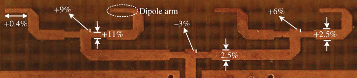
Figure 5.22 Percentage of errors in fabrication process.
5.3.7.2 Antenna Fabrication Error
At 60 GHz, the design would be very sensitive to any error during fabrication process. The effect of fabrication error was shown in the previous section, where inaccurate widths in the array feed network and dipole arms resulted in mismatch between the measured and simulated reflection coefficients. At least two array antennas are required in the proposed technique; therefore, it is important to consider the design robustness to dimensional tolerances as process variation in photolithographic etching always exists. It was discussed earlier that the T-junction power divider provides higher bandwidths when a reactive stub is utilized compared to a conventional V-notch in its structure. Moreover, it was found that the reactive stub significantly influences the design robustness to process errors.
Based on this finding, five samples of fabricated array antennas as shown in Figure 5.23 are measured by a digital microscope. The values of errors in different sections of the array structure are summarized in Table 5.5. As discussed earlier, the width of lines in the printed circuit is more vulnerable to process error than the line length.

Figure 5.23 Five DSPD arrays and highlighted parametrized sections of array.
Table 5.5 Fabrication Variation
| Parameter | Pw | Da | Pt | Ig |
| Error (%) | [−1.5, 3] | [−0.2, 0.4] | [−7, 11] | [−3, 9] |
The measured input impedance, return loss (S11 in dB) versus frequency for the five fabricated array samples and the simulated S11 based on the accurate design values are shown in Figure 5.24. While the measured return losses are not completely matched with the simulation result due to the fabrication error, all five samples have acceptable performance (S11 > 10 dB) in the frequency range 57–64 GHz. Moreover, one may notice that all of the fabricated samples acquire almost the same resonance frequency as suggested through simulation, around 62.8–63.2 GHz. It can also be concluded that irrespective of fabrication error through conventional photolithographic printed circuit board (PCB) fabrication technique, appropriate antenna design at 60 GHz millimeter-band is feasible.

Figure 5.24 Simulated S11 and five measured return losses of sample arrays.
5.3.7.3 Radiation Pattern Measurement
After satisfactory input impedance RL measurement, the radiation patterns of the fabricated array are measured. The array antenna under test (AUT) is set as a receiver antenna and a horn antenna [46], manufactured by Ainfoinc, is used as a standard gain transmitting antenna. Agilent PNA E8361A in its receiver mode is used. Figure 5.25 shows the photograph of the test setup with the standard gain horn antenna mounted on a fixed Perspex pole and the AUT mounted on a turn table. The radiation pattern is measured in every 10° steps for full 360° for both E- and H-plane cuts. Some conical absorbers are placed around the antennas to reduce surrounding interferences. Both measured and simulation copolar and cross-polar radiation patterns at 58, 60, and 63 GHz are shown in Figure 5.26. The measured radiation patterns are in congruence with the simulation results with minor shifts in sidelobe levels.

Figure 5.25 System setup for radiation pattern measurement.

Figure 5.26 Measured and simulated E-plane radiation pattern, co- and cross-polar radiation.
The measured cross-polar result is shown in Figure 5.26. As is clear from Figure 5.26, the CPL is adequately below −20 dB. This is a very satisfactory result considering the effects of the long feedline and the reflection from the large V-type connector.
As it is clear from Figure 5.26, the E-plane pattern is narrow compared with H-plane as the array is vertically aligned. Therefore, the 10° measurement would not be sufficient for the E-plane and to accurately measure the HPBW of the antenna in E-plane, measurements are repeated for every 1° for the ±10° of the boresight direction as shown in Figure 5.27. By considering the manual rotation of AUT in every 1°, small errors may be expected. To minimize this error, the measurement is repeated three times and the average value is considered. Figure 5.27 shows the copolar radiation pattern in ±10° of boresight direction of the array antenna at 58 GHz. It shows that the measured HPBW is smaller compared with the simulated HPBW. Table 5.6 summarizes the HPBW of the array that shows that, for all cases, the measured HPBW are smaller than the simulation result.

Figure 5.27 (a) Measurement setup for 1° accuracy and (b) measured and simulated HPBW of E-plane.
Table 5.6 Simulated and Measured HPBW in E-Plane
| Frequency (GHz) | E-Plane (°) | H-Plane (°) | ||
| Simulated | Measured | Simulated | Measured | |
| 58 | 21 | 15 | 182 | 135 |
| 60 | 18 | 15 | 185 | 135 |
| 63 | 17 | 13 | 190 | 150 |
5.3.7.4 Gain Measurement
The measurement of the array gain is a combination of measurement, simulation, and calculation process. The standard horn antenna is used as transmit antenna and AUT receives the signal, while the Agilent PNA measures the S21 of the link. The gain of the array relates to other parameters by
where GTx is the gain of horn antenna, which is 10.6 dBi. Lcable is the cable loss and can be measured directly with the Agilent PNA E8361A using full two-port error correction calibration. In measuring Lcable, the loss of connectors and adaptors are also considered. Free space loss or path loss, LFS, is calculated using Friis transmission formula [41]. The feedline loss should be considered as the CPW feed extension is 4λ long and contributes significantly to the gain result. This loss has been separately simulated in CST and shown in Figure 5.28. The feedline is primarily designed at 60.5 GHz, which is the center frequency of 57–64 GHz. Therefore, the feedline shows the minimum insertion loss at 60.5 GHz and more loss in other frequencies of the band. The 1.85 mm Southwest Microwave connector has a VSWR of 1.25 [44] means that the impedance mismatch of the connector should not have significant effect on the gain measurement. Therefore, the connector's performance is not excluded from the gain measurement. By considering Equation (5.9) and by combining the measured data with the LFS and simulated Lfeedline, the final value of the gain versus frequency is shown in Figure 5.28. As can be seen from the figure, the feedline loss and antenna gain are congruent to each other over the frequency band. There is about 1.5 dB gain drop from 7 dBi due to 1.5 dB insertion loss variation of the feedline. The absolute gain of the array antenna varies from 5.5 to 7 dBi over the frequency band of operation.

Figure 5.28 Measured gain and simulated feedline loss of array.
5.4 CONCLUSIONS
This chapter discussed about some key technical specifications of the proposed spatial-based system for the chipless RFID system. First it suggested the millimeter-band 60 GHz as the appropriate band for precise scanning of the tag. Then the general situation of the unlicensed 60 GHz band has been reviewed from a technical and regulatory perspective. The low regulatory restrictions on the EIRP of this band have been highlighted that makes the band very suitable for the proposed technique. Moreover, it was shown that the minimum amount of metal is required for the printed tag at this band, which lowers the tag price below that for the barcode.
In the second part of the chapter, the technical and operational necessities of the reader antennas for the proposed technique were reviewed. Based on the proposed application, the technical specifications of the reader antenna were established first. A survey on the available open source products was conducted and their technical specifications were reviewed. The process of the antenna design was then introduced. An array of DSPD antennas was proposed to satisfy the demanded technical specifications. A DSPD array antenna was designed and thoroughly investigated at 60 GHz.
First, the Taconic TLX-8 was characterized using an SIW resonant technique. The measured constitutive parameters at 60 GHz significantly differed from that of published data at 10 GHz. The new values were used for designing a four-element DSPD array antenna. In the design process, the following advanced design techniques were used: (i) a broadband matching technique using dipole arms chamfering and abrupt ground plane for the dipole element, (ii) element array analysis and mitigating mutual coupling between elements, (iii) beam-forming network with matching stub at the T-junction, (iv) microstrip-to-CPW transition and SIW-based CPW extensions, and finally (v) a V-type connector assembly. The array of four DSPD elements covered the whole frequency range of 57–64 GHz yielding 12% bandwidth. While the array dimension was very small and the standard printed circuit board technology was used for the antenna fabrication, the measurement results were well matched with the simulation predictions. The measured CPL was below −20 dB as required for proper operation of the spatial-based system. The measured gain of the array was 5.5–7 dBi over the entire frequency range of operation. The size of the array was 22 ![]() 14 mm2. The compact and simple structure of the array also made it suitable for many applications in the millimeter-wave region for low-range wireless communication systems.
14 mm2. The compact and simple structure of the array also made it suitable for many applications in the millimeter-wave region for low-range wireless communication systems.
REFERENCES
- 1. ITU-R, “Rec.p 676-9, Attenuation by Atmospheric Gases,” International Telecommunication Union, Geneva, 2012.
- 2. C. Koh, “The Benefits of 60 GHz Unlicensed Wireless Communications,” YDI Company, USA.
- 3. ITU, Radio Regulation, ITU, Geneva, 2012.
- 4. S.K. Yong, P. Xia, and A.V. Garcia, 60 GHz Technology for Gbps WLAN and WPAN: From Theory to Practice. John Wiley & Sons UK, 2010.
- 5. N. Guo, R.C. Qiu, Sh.S. Mo, and K. Takahashi, “60-GHz Millimeter-Wave Radio: Principle, Technology, and New Results,” EURASIP Journal on Wireless Communications and Networking, vol. 2007, pp. 1–9, 2007.
- 6. ACMA, “60 GHz Band, Millimetre Wave Technology,” 2004.
- 7. S. Yong and C. Chong, “An Overview of Multi Giga bit Wireless through Millimeter Wave Technology: Potentials and Technical Challenges,” EURASIP Journal on Wireless Communications and Networking, vol. 2007, p. 10, 2007.
- 8. S. Yong, P. Xia, and A.V. Garcia, 60 GHz Technology for Gbps WLAN and WPAN, John & Wiley, 2010.
- 9. W. Buchar, N. Karmakar, and M.Zomorrodi, “MIMO-Based Technique for Chipless RFID EM-Imaging at 60 GHz,” Grant proposal Xerox, USA Sep 2014.
- 10. HURZ Stamping Technology, (Feb 2015). Available: http://www.kurz.de.
- 11. ACMA, “LIPD Regulation,” 2011.
- 12. ACMA, “Radiocommunications (Low Interference Potential Devices) Class Licence 2000,” ACMA, Canberra 2011.
- 13. Comlab Inc., Nokia. (14 Oct 2014). Radio Link Systems Nokia MetroHopper 58 GHz. Available: www.comlab.hut.fi/studies.
- 14. Proxim Wireless Inc., Oct 2014). Terabeam Product. Available: http://www.proxim.com/.
- 15. A. Nesic, S. Jovanovic, and V. Brankovic, “Design of Printed Dipoles Near The Third Resonance,” in Antennas and Propagation Society International Symposium, Atlanta, GA, USA, 1998, pp. 928–931.
- 16. R.B. Waterhouse, D. Novak, A. Nirmalathas, and C. Lim, “Broadband Printed Sectorized Coverage Antennas for Millimeter-Wave Wireless Applications,” IEEE Transactions on Antennas and Propagation, vol. 50, pp. 12–16, 2002.
- 17. W. Menzel, “A 40 GHz Printed Array Antenna,” in Digest, pp. 225–226, 1980.
- 18. C. Peixeiro, P. Dufrane, and Y. Gullerme, “Microstrip Patch Antennas for a Mobile Communications System at 60 GHz,” in Antennas and Propagation Society International Symposium, AP-S, Digest, Baltimore, MD, USA, 1996.
- 19. T.G. Ma and S.K. Jeng, “A Printed Dipole Antenna with Tapered Slot Feed for Ultrawide Band Applications,” IEEE Transactions on Antennas and Propagation, vol. 53, pp. 3833–3839, 2005.
- 20. M. Scott, “A Printed Dipole for Wide-Scanning Array Application,” in IEEE 11th International Conference on Antennas and Propagation, 2001, pp. 37–40.
- 21. Y.H. Suh and K. Chang, “A New Millimeter-Wave Printed Dipole Phased Array Antenna Using Microstrip-Fed Coplanar Stripline Tee Junctions,” IEEE Transactions on Antennas and Propagation, vol. 52, pp. 2019–2027, 2004.
- 22. V. Brankovic and A. Nesic, “Wide Band Printed Phase Array Antenna for Microwave and mm-Wave Applications,” US Patent, March 2000.
- 23. R.A. Alhalabi and G.M. Rebeiz, “High-Efficiency Angled-Dipole Antennas for Millimeter-Wave Phased Array Applications,” IEEE Transactions on Antennas and Propagation, vol. 56, p. 7, 2008.
- 24. Y.C. Chiou, R.A. Alhalabi, and G.M. Rebeiz, “High-Efficiency 60 GHz Dipole-Box Antennas,” in Antennas and Propagation Society International Symposium (APSURSI), 2010.
- 25. P. Kalansuriya, N.C. Karmakar, and E. Viterbo, “On the Detection of Frequency-Spectra-Based Chipless RFID Using UWB Impulsed Interrogation,” IEEE Transactions on Microwave Theory and Techniques, vol. 60, pp. 4187–4197, 2012.
- 26. Taconic, “Taconic Laminate Material Guide,” 2014.
- 27. R. Anita and M.V.C. Kumar, “Analysis of Triangular Microstrip Patch Antenna for Different Antenna,” in JREAT International Journal of Research in Engineering & Advanced Technology, 2013.
- 28. H.R. Fettermana, T.C.L.G. Sollnera, P.T. Parrisha, D. Parkera, H. Mathewsa, and P.E. Tannenwalda, “Printed Dipole Millimeter Antenna for Imaging Array Applications,” Electromagnetics, vol. 3, pp. 209–215, 1983.
- 29. D.M. Pozar, “Considerations for Millimeter Wave Printed Antennas,” IEEE Transactions on Antennas and Propagation, vol. 31, No. 5, p. 8, 1983.
- 30. P. Katehi and N. Alexopoulos, “On the Effect of Substrate Thickness and Permittivity on Printed Circuit Dipole Properties” IEEE Transactions on Antennas and Propagation, vol. 31, p. 6, 1983.
- 31. W. Hong and K. Wu, “94 GHz Substrate Integrated Monopulse Antenna Array,” IEEE Transactions on Antennas and Propagation, vol. 60, pp. 121–129, 2011.
- 32. J. Sheen, “Comparisons of Microwave Dielectric Property Measurements by Transmission/Reflection Techniques and Resonance Techniques,” Measurement Science and Technology, vol. 20, pp. 1–12, 2009.
- 33. D.E. Zelenchuk, V. Fusco, G. Goussetis, A. Mendez, and D. Linton, “Millimeter-Wave Printed Circuit Board Characterization Using Substrate Integrated Waveguide Resonators,” IEEE Transactions on Microwave Theory and Technique, vol. 60, 3300–3308, 2012.
- 34. M. Bozzi and L. Perregrini, “Modeling of Conductor, Dielectric, and Radiation Losses in Substrate Integrated Waveguide by the Boundary Integral-Resonant Mode Expansion Method,” IEEE Transactions on Microwave Theory and Techniques, vol. 56, pp. 3153–3161, 2008.
- 35. W.L. Stutzman and G.A. Thiele, Antenna Theory and Design, John Wiley & Sons, 1981.
- 36. G.Y. Chen and J.Sh. Sun, “A Printed Dipole Antenna with Microstrip Tapered Balun,” Microwave and Optical Technology Letters, vol. 40, pp. 344–346, 2004.
- 37. R.J.P. Douvilie and D.S. James, “Experimental Study of Symmetric Microstrip Bends and Their Compensation,” IEEE Transactions on Microwave Theory and Technique, vol. 26, p. 175, 1978.
- 38. S. Preradovic, “Chipless RFID System for Barcode Replacement,” PhD, ECSE, Monash University, 2009.
- 39. S.M. Roy, “Development of a Frequency Encoded Chipless RFID Tag,” PhD, ECSE, Monash University, 2008.
- 40. R.L. Haupt, Antenna Arrays, A Computational Approach. Pennsylvania State University, State College, John Wiley&Sons, Inc., Publication, Pennsylvania, 2010.
- 41. C.A. Balanis, Antenna Theory Analysis and Design, Third ed.. John Wiley & Sons, Hoboken, New Jersey, , 2005.
- 42. D. M. Pozar, Microwave Engineering, Third ed., John Wiley & Sons, 2005.
- 43. J. Coonrod, “Comparing Microstrip and CPW Performance,” Microwave Journal, vol. 55, pp. 74–82, 2012.
- 44. Southwest Microwave, Inc., S. Microwave. “1.85 mm Connectors”. Available: www.southwestmicrowave.com/.
- 45. (2013). SouthWest Microwave. Available: www.southwestmicrowave.com.
- 46. Ainfoinc Company, (14 March 2012). Ainfoinc Company. Available: http://www.ainfoinc.com.