
RF Technologies at mm-Wave Frequencies
Abstract
This chapter describes some of the RF technologies needed at mm-Wave frequencies to implement devices and BS in frequency range 2. Challenges and possibilities are discussed for different implementation alternatives.
Keywords
mm-Wave technologies; ACD; DAC; LO generation; phase noise; power amplifier; filtering; noise figure; dynamic range; bandwidth
The existing 3GPP specifications for 2G, 3G, and 4G mobile communications are applicable to frequency ranges below 6 GHz and the corresponding RF requirements consider the technology aspects related to below 6 GHz operation. NR also operates in those frequency ranges (identified as frequency range 1) but will in addition be defined for operation above 24.25 GHz (frequency range 2 or FR2), also referred to as mm-wave frequencies. A fundamental aspect for defining the RF performance and setting RF requirements for NR base stations and devices is the change in technologies used for RF implementation in order to support operation in those higher frequencies. In this chapter, some important and fundamental aspects related to mm-wave technologies are presented in order to better understand the performance that mm-wave technology can offer, but also what the limitations are.
In this chapter, Analog-to-Digital/Digital-to-Analog converters and power amplifiers are discussed, including aspects such as the achievable output power versus efficiency and linearity. In addition, some detailed insights are provided into receiver essential metrics such as noise figure, bandwidth, dynamic range, power dissipation, and the dependencies between metrics. The mechanism for frequency generation and the related phase noise aspects are also covered. Filters for mm-waves are another important part, indicating the achievable performance for various technologies and the feasibility of integrating filters into NR implementations.
The data sets used in this chapter indicate the current state-of-the-art capability and performance and are either published elsewhere or have been presented as part of the 3GPP study for developing NR [11]. Note that neither the 3GPP specifications nor the discussion here mandate any restrictions, specific models, or implementations for NR in frequency range 2. The discussion highlights and analyzes different possibilities for RF implementation of mm-wave receivers and transmitters.
An additional aspect is that essentially all operation in Frequency Range 2 will be with Active Antenna System base stations using large antenna array sizes and devices with multi-antenna implementations. While this is enabled by the smaller scale of antennas at mm-wave frequencies, it also drives complexity. The compact building practice needed for mm-wave systems with many transceivers and antennas requires careful and often complex consideration regarding the power efficiency and heat dissipation within a small area or volume. These considerations directly affect the achievable performance and possible RF requirements. The discussion here in many aspects applies for both NR base stations and NR devices, noting also that the mm-wave transceiver implementation between device and base station will have less differences compared to frequency bands below 6 GHz.
19.1 ADC and DAC Considerations
The larger bandwidths available at mm-wave communication will challenge the data conversion interfaces between analog and digital domains in both receivers and transmitters. The signal-to-noise-and-distortion ratio (SNDR)-based Schreier Figure-of-Merit (FoM) is a widely accepted metric for Analog-to-Digital Converters (ADCs) defined by [61]
with SNDR in dB, power consumption P in W, and Nyquist sampling frequency fs in Hz. Fig. 19.1 shows the Schreier FoM for a large number of ADCs vs the Nyquist sampling frequency fs (=2×BW for most converters), published at the two most acknowledged conferences [62] in this field of research. The dashed line indicates the FoM envelope which is constant at roughly 180 dB for sampling frequencies below some 100 MHz. With constant FoM, the power consumption doubles for every doubling of bandwidth or 3 dB increase in SNDR. Above 100 MHz there is an additional 10 dB/decade penalty, and this means that a doubling of bandwidth will increase power consumption by a factor of 4.

Although the FoM envelope is expected to be slowly pushed towards higher frequencies by continued development of integrated circuit technology, RF bandwidths in the GHz range inevitably give poor power efficiency in the analog-to-digital conversion. The large bandwidths and array sizes assumed for NR at mm-wave will thus lead to a large ADC power footprint and it is important that specifications driving SNDR requirements are not unnecessarily high. This applies to devices as well as base stations.
Digital-to-Analog Converters (DACs) are typically less complex than their ADC counterparts for the same resolution and speed. Furthermore, while ADC operation commonly involves iterative processes, the DACs do not. DACs also attract substantially less interest in the research community. While structurally quite different from their ADC counterparts they can still be benchmarked using the same FoM and render similar numbers as for ADCs. In the same way as for ADC, a larger bandwidth and unnecessarily high SNDR requirement on the transmitter will result in higher DAC power footprint.
19.2 LO Generation and Phase Noise Aspects
Local Oscillator (LO) is an essential component in all modern communication systems for shifting carrier frequency up- or downwards in transceivers. A parameter featuring the LO quality is the so-called phase noise (PN) of the signal generated by the LO. In plain words, phase noise is a measure of how stable the signal is in frequency domain. Its value is given in dBc/Hz for an offset frequency Δf and it describes the likelihood that the oscillation frequency deviates by Δf from the desired frequency.
LO phase noise may significantly impact system performance; this is illustrated in Fig. 19.2, though somewhat exaggerated for a single-carrier example, where the constellation diagram for a 16-QAM signal is compared for cases with and without phase noise, including in both cases an Additive White Gaussian Noise (AWGN) signal modeling thermal noise. For a given symbol error rate, phase noise limits the highest modulation scheme that may be utilized, as demonstrated in Fig. 19.2. In other words, different modulation schemes pose different requirements on the LO phase noise level.

19.2.1 Phase Noise Characteristics of Free-Running Oscillators and PLLs
The most common circuit solution for frequency generation is to use a Voltage-Controlled Oscillator (VCO). Fig. 19.3 shows a model and the characteristic PN behavior of a free-running VCO in different offset frequency regions, where f0 is the oscillation frequency, Δf is the offset frequency from f0, Ps is the signal strength, Q is the loaded quality factor of the resonator, F is an empirical fitting parameter but has physical meaning of noise figure, and Δf1/f3 is the 1/f-noise corner frequency of the active device in use [57].

The following can be concluded from the Leeson formula in Fig. 19.3:
- 1. PN increases by 6 dB per every doubling of the oscillation frequency f0;
- 2. PN is inversely proportional to signal strength, Ps;
- 3. PN is inversely proportional to the square of the loaded quality factor of the resonator, Q;
- 4. 1/f noise up-conversion gives rise to close-to-carrier PN increase (at small offset).
Thus, there are several parameters that may be used for design trade-offs in VCO development. To make performance comparison of the VCOs made in different semiconductor technologies and circuitry topologies, a Figure-of-Merit (FoM) is often used which takes into account power consumption and thus allows for a fair comparison:
Here ![]() is the phase noise of the VCO in dBc/Hz and
is the phase noise of the VCO in dBc/Hz and ![]() is the power consumption in watt. One noticeable result of this expression is that both phase noise and power consumption in linear power are proportional to
is the power consumption in watt. One noticeable result of this expression is that both phase noise and power consumption in linear power are proportional to ![]() 2. Thus, to maintain a phase noise level at a certain offset while increasing
2. Thus, to maintain a phase noise level at a certain offset while increasing ![]() by a factor N would require the power to be increased by N2 (assuming a fixed FoM value).
by a factor N would require the power to be increased by N2 (assuming a fixed FoM value).
A common way to suppress the phase noise is to apply a Phase Locked Loop (PLL) [18]. Basic PLL building blocks contain a VCO, frequency divider, phase detector, loop filter, and a low-frequency reference source of high stability, such as a crystal oscillator. The total phase noise of the PLL output is composed of contributions from the VCO outside the loop bandwidth and the reference oscillator inside the loop. A significant noise contribution is also added by the phase detector and the divider.
As an example for the typical behavior of an mm-wave LO, Fig. 19.4 shows the measured phase noise from a 28 GHz LO produced by applying a PLL at a lower frequency and then multiplying up to 28 GHz. There are four different offset ranges that show distinctive characteristics:
- 1. f1, for small offset, <10 kHz: ~30 dB/decade roll-off, due to 1/f noise up-conversion;
- 2. f2, for offset within the PLL bandwidth: relatively flat and composed of several contributions;
- 3. f3, for offset larger than PLL bandwidth: ~20 dB/decade roll-off, dominant by VCO phase noise;
- 4. f4, for even larger offset, >10 MHz: flat, due to finite noise floor.

19.2.2 Challenges With mm-Wave Signal Generation
As phase noise increases with frequency, increasing the oscillation frequency from 3 GHz to 30 GHz, for instance, will result in fundamental PN degradation of 20 dB at a given offset frequency. This will certainly limit the highest order of PN-sensitive modulation schemes usable at mm-wave and thus poses a limitation on achievable spectrum efficiency for mm-wave communications.
Millimeter-wave LOs also suffer from the degradation in quality factor Q and the signal power Ps. Leeson’s equation tells us that in order to achieve low phase noise, Q and Ps need to be maximized, while minimizing the noise figure of the active device. Unfortunately, these three factors contribute in an unfavorable manner when oscillation frequency increases. In monolithic VCO implementation, the Q-value of the on-chip resonator decreases rapidly with frequency increases due mainly to (1) the increase of parasitic losses such as metal loss and/or substrate loss and (2) the decrease of varactor Q. Meanwhile, the signal strength of the oscillator becomes increasingly limited when going to higher frequencies. This is because higher-frequency operation requires more advanced semiconductor devices whose breakdown voltage decreases as their feature size shrinks. This is manifested by the observed reduction in power capability versus frequency for power amplifiers (–20 dB per decade) as detailed in Section 19.3. For this reason, a method widely applied in mm-wave LO implementation is to generate a lower-frequency PLL and then multiply the signal up to the target frequency.
Except for the challenges discussed above, up-conversion of the 1/f noise creates an added slope close to the carrier. The 1/f noise is strongly technology-dependent, where planar devices such as CMOS and HEMT (High Electron Mobility Transistor) generally show higher 1/f noise than vertical bipolar devices such as bipolar and HBTs. Technologies used in fully integrated MMIC/RFIC VCO and PLL solution range from CMOS and BiCMOS to III–V materials where InGaP HBT is popular due to its relatively low 1/f noise and high breakdown. Occasionally also pHEMT devices are used, even if suffering from severe 1/f noise. Some developments have been made using GaN FET structures in order to benefit from the very high breakdown voltage, but 1/f is even higher than in GaAs FET devices and therefore seems to offset the gain due to the breakdown voltage. Fig. 19.5 summarizes phase noise performance at 100 kHz offset vs oscillation frequency for different semiconductor technologies.

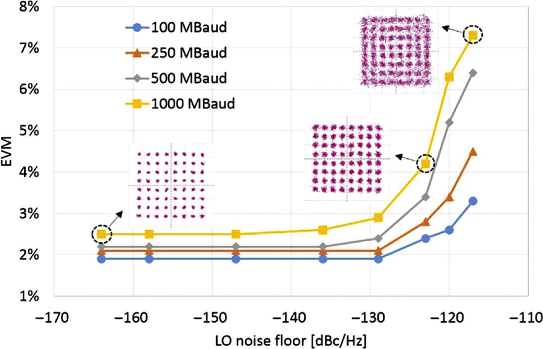
Last but not least, recent research reveals the impact of the LO noise floor on system performance [23]. This impact is insignificant if the symbol rate is low. When the rate increases, such as in 5G NR, the flat noise floor starts to increasingly affect the EVM of the modulated signal. Fig. 19.6 shows the measured EVM from a transmitter for different symbol rate and different noise floor level. The impact from receiver LO noise floor is similar. This observation may imply that it requires extra care when generating mm-wave LOs for wideband systems in terms of choice of technology, VCO topology, and multiplication factor, to maintain a reasonably low PN floor.
19.3 Power Amplifier Efficiency in Relation to Unwanted Emission
Radio Frequency (RF) building block performance generally degrades with increasing frequency. The power capability of power amplifiers (PA) for a given integrated circuit technology roughly degrades by 20 dB per decade, as shown in Fig. 19.7 for a number of various semiconductor technologies. There is a fundamental cause for this degradation; increased power capability and increased frequency capability are conflicting requirements as observed from the so-called Johnson limit [54]. In short, higher operational frequencies require smaller geometries, which subsequently result in lower operational power in order to prevent dielectric breakdown from the increased field strengths. To uphold Moore’s law, the gate geometries are constantly shrunk and hence the intrinsic power capability is reduced.

A remedy is however found in the choice of integrated circuit material. mm-Wave integrated circuits have traditionally been manufactured using so-called III–V materials, that is a combination of elements from groups III and V of the periodic table, such as Gallium Arsenide (GaAs) and more recently Gallium Nitride (GaN). Integrated circuit technologies based on III–V materials are substantially more expensive than conventional silicon-based technologies and they cannot handle the integration complexity of, for example, digital circuits or radio modems for cellular handsets. Nevertheless, GaN-based technologies are now maturing rapidly and deliver power levels an order of magnitude higher compared to conventional technologies.
There are mainly three semiconductor material parameters that affect the efficiency of an amplifier: maximum operating voltage, maximum operating current density, and knee-voltage. Due to the knee-voltage, the maximum attainable efficiency is reduced by a factor that is proportional to:
where k is the ratio of knee-voltage to the maximum operating voltage. For most transistor technologies the ratio k is in the range of 0.05–0.01, resulting in an efficiency degradation of 10%–20%.
The maximum operating voltage and the current density limit the maximum output power from a single transistor cell. To further increase the output power, the output from multiple transistor cells must be combined. The most common combination techniques are stacking (voltage combining), paralleling (current combining), and corporate combiners (power combining). Either choice of combination technique will be associated with a certain combiner-efficiency. A lower power density requires more combination stages and will incur a lower overall combiner-efficiency. At mm-wave frequencies the voltage- and current-combining methods are limited due to the wave-length. The overall size of the transistor cell must be kept less than about 1/10th of the wavelength. Hence, paralleling and/or stacking are used to some extent and then corporate combining is used to get the wanted output power. The maximum power density of CMOS is about 100 mW/mm compared to 4000 mW/mm for GaN. Thus, GaN technology will require less aggressive combining strategies and hence give higher efficiency.
Fig. 19.8 shows the saturated power-added efficiency (PAE) as a function of frequency. The maximum reported PAE is approximately 40% and 25%, at 30 GHz and 77 GHz, respectively.

PAE is expressed as
At mm-wave frequencies, semiconductor technologies fundamentally limit the available output power. Furthermore, the efficiency is also degraded with higher frequency.
Considering the PAE characteristics in Fig. 19.8, and the non-linear behavior of the AM-AM/AM-PM characteristics of the power amplifier, significant power back-off may be necessary to reach linearity requirement such as the transmitter ACLR requirements (see Section 18.9). Considering the heat dissipation aspects and significantly reduced area/volume for mm-wave products, the complex interrelation between linearity, PAE, and output power in the light of heat dissipation must be considered.
19.4 Filtering Aspects
Using various types of filters in base station and device implementations is an essential component for meeting the overall RF requirements. This has been the case for all generations of mobile systems and will be essential also for NR, both below 6 GHz and in the new mm-wave bands. The filters mitigate the unwanted emissions arising from, for example, non-linearity in the transmitters generated due to intermodulation, noise, harmonics generation, LO leakage, and various unwanted mixing products. In the receiver chain, filters are used to handle either self-interference from own transmitter signal in paired bands, or to suppress the interferer at adjacent or other frequencies.
The RF requirements are differentiated in terms of levels for different scenarios. For base station spurious emission, there are general requirements across a very wide frequency range, coexistence requirements in the same geographical areas, and co-location requirements for dense deployments. Similar requirements are defined for devices.
Considering the limited size (area/volume) and level of integrations needed for mm-wave frequencies, the filtering can be challenging where discrete mm-wave filters are quite bulky and there is a challenge to embed such filters into highly integrated structures for mm-wave products.
19.4.1 Possibilities of Filtering at the Analog Front-End
Different implementations provide different possibilities for filtering. For the purpose of discussion, two main cases can be identified:
- • Low-cost, monolithic integration with one or a few multi-chain CMOS/BiCMOS core-chips with built-in power amplifiers and built in down-converters. This case will give limited possibilities to include high-performance filters along the RF-chains since the Q-values for on chip filter resonators will be poor (5–20).
- • High-performance, heterogeneous integration with several CMOS/BiCMOS core chips, combined with external amplifiers and external mixers. This implementation allows the inclusion of external filters along the RF-chains (at a higher complexity, size, and power consumption).
There are at least three places where it makes sense to put filters, depending on implementation, as shown in Fig 19.9:
- • Behind or inside the antenna element (F1 or F0), where loss, size, cost, and wide-band suppression are important;
- • Behind the first amplifiers (looking from the antenna side), where low loss is less critical (F2);
- • On the high-frequency side of mixers (F3), where signal have been combined (in the case of analog and hybrid beam forming).

The main purpose of F1/F0 is normally to suppress interference and emissions far from the desired channel across a wide frequency range (for example, DC to 60 GHz). There should not be any unintentional resonances or passbands in this wide frequency range. This filter will help relax the design challenge (bandwidth to consider, linearity requirements, etc.) of all following blocks. Insertion loss must be very low, and there are strict size and cost requirements since there must be one filter at each subarray (Figs. 19.9 and 19.10). In some cases, this filter must fulfill strict suppression requirements close to the passband, particularly for high output power close to sensitive bands.

The main purpose of F2 is suppression of LO-, image-, spurious-, and noise-emission, and suppression of incoming interferers relatively far from the desired frequency band. There are still strict size requirements, but more loss can be accepted (behind the first amplifiers) and even unintentional passbands (assuming F1/F0 will handle that). This allows better discrimination (more poles), and better frequency precision (for example, using half-wave resonators).
The main purpose of F3 is typically suppression of LO-, image-, spurious-, and noise-emission, and suppression of incoming interferers that accidentally fall in the IF-band after the mixer, and strong interferers that tend to block the mixers or ADCs. For analog (or hybrid) beam-forming it is enough to have just one (or a few) such filters. This relaxes requirements on size and cost, which opens the possibility to achieve sharp filters with multiple poles and zeroes, and with high Q-value and good frequency precision in the resonators.
The deeper into the RF-chain (starting from the antenna element), the better protected the circuits will get. For the monolithic integration case it is difficult to implement filters F2 and F3. One can expect performance penalties for this case, and output power per branch is lower. Furthermore, it is challenging to achieve good isolation across a wide frequency range, as microwaves tend to bypass filters by propagating in ground structures around them.
19.4.2 Insertion Loss (IL) and Bandwidth
Sharp filtering on each branch (at positions F1/F0) with narrow bandwidth leads to excessive loss at microwave and mm-wave frequencies. To get the insertion loss down to a reasonable level the passband can be made significantly larger than the signal bandwidth. A drawback of such an approach is that more unwanted signals will pass the filter. In choosing the best loss-bandwidth trade-off there are some basic dependencies to be aware of:
To exemplify the trade-off, a three-pole LC-filter with Q=20, 100, 500, and 5000, for 100 and 800 MHz 3 dB-bandwidth is studied, tuned to 15 dB return loss (with Q=5000) is examined, as shown in Fig. 19.11.

From this study it is observed that:
- • 800 MHz bandwidth or smaller, requires exotic filter technologies, with a Q-value around 500 or better to get an IL below 1.5 dB. Such Q-values are very challenging to achieve considering constraints on size, integration aspects, and cost;
- • By relaxing the requirement on selectivity to 4×800 MHz, it is sufficient to have a Q-value around 100 to get 2 dB IL. This should be within reach with a low-loss printed circuit board (PCB). The increased bandwidth will also help to relax the tolerance requirements on the PCB.
19.4.3 Filter Implementation Examples
There are many ways to implement filters in a 5G array radio. Key aspects to compare are: Q-value, discrimination, size, and integration possibilities. Table 19.1 gives a rough comparison between different technologies and two specific examples are given below.
Table 19.1

19.4.3.1 PCB Integrated Implementation Example
A simple and attractive way to implement antenna filters (F1) is to use strip-line or microstrip filters, embedded in a PCB close to each antenna element. This requires a low-loss PCB with good precision. Production tolerances (permittivity and patterning and via-positioning) will limit the performance, mainly though a shift in the pass-band and increased mismatch. In most implementations the passband must be set larger than the operating frequency band with a significant margin to account for this.
Typical characteristics of such filters can be illustrated by looking at the following design example, with the layout shown in Fig. 19.12:

The filter is tuned to give 20 dB suppression at 24 GHz, while passing as much as possible of the band 24.25–27.5 GHz (with 17 dB return loss). Significant margins are added to make room for variations in the manufacturing processes of the PCB.
A Monte Carlo analysis was performed to study the impact of variations in the manufacturing process on filter performance, using the following quite aggressive tolerance assumptions for the PCB:
With these distribution assumptions, 1000 instances of the filter were generated and simulated. Fig. 19.13 shows the filter performance (S21) for these 1000 instances (blue traces), together with the nominal performance (yellow trace). Red lines in the graph indicate possible requirement levels that could be met considering this filter.

From this design example, the following rough description of a PCB filter implementation is found:
- • 3–4 dB insertion loss;
- • 20 dB suppression (17 dB if IL is subtracted);
- • 1.5 GHz transition region with margins included;
- • Size: 25 mm2, which can be difficult to fit in the case of individual feed and/or dual polarized elements;
- • If a 3 dB IL is targeted, there would be significant yield loss with the suggested requirement, in particular for channels close to the pass-band edges.
19.4.3.2 LTCC Filter Implementation Example
Another promising way to implement filters is to make components for Surface Mount Assembly (SMT), including both filters and antennas, for example based on Low-Temperature Cofired Ceramics (LTCC). One example of a prototype LTCC component was outlined in Ref. [31] and is also shown in Fig. 19.14.

The measured performance of the corresponding filter is shown in Fig. 19.15 and it shows that the LTCC-filter adds about 2 dB of insertion loss for a 2 GHz passband, while providing 22 dB of additional attenuation 1 GHz from the passband edge.

Additional margins relative to this example should be considered to account for manufacturing tolerances and future adjustments of bandwidth, suppression level, guard bandwidth, antenna properties, integration aspects, etc. Accounting for such margins, the LTCC-filter shown could be assumed to add approximately 3 dB of insertion loss, for 17 dB suppression (IL subtracted) at 1.5 GHz from the pass-band edge.
Technology development, particularly regarding Q-values and manufacturing tolerances, will likely lead to improvements in these numbers.
19.5 Receiver Noise Figure, Dynamic Range, and Bandwidth Dependencies
19.5.1 Receiver and Noise Figure Model
A receiver model as shown in Fig. 19.16 is assumed here. The dynamic range (DR) of the receiver will in general be limited by the front-end insertion loss (IL), the receiver (RX) Low-noise Amplifier (LNA), and the ADC noise and linearity properties.

Typically DRLNA![]() DRADC so the RX use Automatic Gain Control (AGC) and selectivity (distributed) in-between the LNA and the ADC to optimize the mapping of the wanted signal and the interference to the DRADC. For simplicity, a fixed gain setting is considered here.
DRADC so the RX use Automatic Gain Control (AGC) and selectivity (distributed) in-between the LNA and the ADC to optimize the mapping of the wanted signal and the interference to the DRADC. For simplicity, a fixed gain setting is considered here.
A further simplified receiver model can be derived by lumping the Front End (FE), RX, and ADC into three cascaded blocks, as shown in Fig. 19.17. This model cannot replace a more rigorous analysis but will demonstrate interdependencies between the main parameters.

Focusing on the small signal co-channel noise floor, the impact of various signal and linearity impairments can be studied to arrive at a simple noise factor, or noise figure, expression.
19.5.2 Noise Factor and Noise Floor
Assuming matched conditions, Friis’ formula can be used to find the noise factor at the receiver input as (linear units unless noted),
The RX input referred small-signal co-channel noise floor will then equal
where N0=k ··· T ··· BW and NADC are the available noise power and the ADC effective noise floor in the channel bandwidth, respectively (k and T being Boltzmann’s constant and absolute temperature, respectively). The ADC noise floor is typically set by a combination of quantization, thermal, and intermodulation noise, but here a flat noise floor is assumed as defined by the ADC effective number of bits.
The effective gain G from LNA input to ADC input depends on small-signal gain, AGC setting, selectivity, and desensitization (saturation), but here it is assumed that the gain is set such that the antenna referred input compression point (CPi) corresponds to the ADC clipping level, that is the ADC full scale input voltage (VFS).
For weak non-linearities, there is a direct mathematical relationship between CP and the third-order intercept point (IP3), such that IP3≈CP+10 dB. For higher-order non-linearities, the difference can be larger than 10 dB, but then CP is still a good estimate of the maximum signal level while intermodulation for lower signal levels may be overestimated.
19.5.3 Compression Point and Gain
Between the antenna and the RX there is the FE with its associated insertion loss (IL>1), for example due to a T/R switch, a possible RF filter, and PCB/substrate losses. These losses have to be accounted for in the gain and noise expressions. Knowing IL, the CPi can be found that corresponds to the ADC clipping as
The antenna referred noise factor and noise figure will then become
and
respectively.
When comparing two designs, for example, at 2 and 30 GHz, respectively, the 30 GHz IL will be significantly higher than that of the 2 GHz. From the Fi expression it can be seen that to maintain the same noise figure (NFi) for the two carrier frequencies, the higher FE loss at 30 GHz needs to be compensated for by improving the RX noise factor. This can be accomplished by (1) using a better LNA, (2) relaxing the input compression point, that is increasing G, or (3) increasing the DRADC. Usually a good LNA is already used at 2 GHz to achieve a low NFi, so this option is rarely possible. Relaxing CPi is an option but this will reduce IP3 and the linearity performance will degrade. Finally, increasing DRADC comes at a power consumption penalty (4× per extra bit). Especially wideband ADCs may have a high power consumption, that is when BW is below some 100 MHz the N0 ··· DRADC product (that is BW ··· DRADC) is proportional to the ADC power consumption, but for higher bandwidths the ADC power consumption is proportional to BW2 ··· DRADC, thereby penalizing higher BW (see Section 19.1). Increasing DRADC is typically not an attractive option and it is inevitable that the 30 GHz receiver will have a significantly higher NFi than that of the 2 GHz receiver.
19.5.4 Power Spectral Density and Dynamic Range
A signal consisting of many similar subcarriers will have a constant power-spectral density (PSD) over its bandwidth and the total signal power can then be found as P=PSD ··· BW.
When signals of different bandwidths but similar power levels are received simultaneously, their PSDs will be inversely proportional to their BW. The antenna-referred noise floor will be proportional to BW and Fi, or Ni =Fi ··· k ··· T ··· BW, as derived above. Since CPi will be fixed, given by G and ADC clipping, the dynamic range, or maximum SNR, will decrease with signal bandwidth, that is SNRmax∝1/BW.
The above signal can be considered as additive white Gaussian noise (AWGN) with an antenna-referred mean power level (Psig) and a standard deviation (σ). Based on this assumption the peak-to-average-power ratio can be approximated as PAPR=20 ··· log10(k), where the peak signal power is defined as Psig+k ··· σ, that is there are k standard deviations between the mean power level and the clipping level. For OFDM an unclipped PAPR of 10 dB is often assumed (that is 3σ) and this margin must be subtracted from CPi to avoid clipping of the received signal. An OFDM signal with an average power level, for example, 3σ below the clipping level will result in less than 0.2% clipping.
19.5.5 Carrier Frequency and mm-Wave Technology Aspects
Designing a receiver at, for example, 30 GHz with a 1 GHz signal bandwidth leaves much less design margin than what would be the case for a 2 GHz carrier frequency, fcarrier with, for example, 50 MHz signal bandwidth. The IC technology speed is similar in both cases but the design margin and performance depend on the technology being much faster than the required signal processing, which means that the 2 GHz design will have better performance.
The graph shows expected evolution of some transistor parameters important for mm-wave IC design, as predicted by the International Technology Roadmap for Semiconductors (ITRS). Here ft, fmax, and Vdd/BVceo data from the ITRS 2007 targets [39] for CMOS and bipolar RF technologies are plotted vs the calendar year when the technology is anticipated to become available. ft is the transistor transit frequency (that is, where the RF device's current gain is 0 dB), and fmax is the maximum frequency of oscillation (that is, when the extrapolated power gain is 0 dB). Vdd is the RF/high-performance CMOS supply voltage and BVceo is the bipolar transistor’s collector–emitter base open breakdown voltage limits. For example, an RF CMOS device is expected to have a maximum Vdd of 750 mV by 2020 (other supply voltages will be available as well, but at a lower speed).
The free space wavelength at 30 GHz is only 1 cm, which is one tenth of what is the case for existing 3GPP bands below 6 GHz. Antenna size and path loss are related to wavelength and carrier frequency, and to compensate the small physical size of a single antenna element multiple antennas, for example, array antennas will have to be used. When beam-forming is used the spacing between antenna elements will still be related to the wavelength, constraining the size of the FE and RX. Some of the implications of these frequency and size constraints are:
- • The ratios ft/fcarrier and fmax/fcarrier will be much lower at millimeter wave frequencies than for below 6 GHz applications. As receiver gain drops with operating frequency when this ratio is less than some 10−100×, the available gain at millimeter waves will be lower and consequently the device noise factor, Fi, higher (similar to when Friis’ formula was applied to a transistor’s internal noise sources).
- • The semiconductor material’s electrical breakdown voltage (Ebr) is inversely proportional to the charge carrier saturation velocity (Vsat) of the device due to the Johnson limit. This can be expressed as Vsat ··· Ebr=constant or fmax ··· Vdd=constant. Consequently, the supply voltage will be lower for millimeter-wave devices compared to devices in the low GHz frequency range. This will limit the CPi and the maximum available dynamic range.
- • A higher level of transceiver integration is required to save space, either as system-on-chip (SoC) or system-in-package (SiP). This will limit the number of technologies suitable for the RF transceiver and limit FRX.
- • RF filters will have to be placed close to the antenna elements and fit into the array antenna. Consequently, they have to be small, resulting in higher physical tolerance requirements, possibly at the cost of insertion loss and stop-band attenuation. That is, IL and selectivity get worse. The filtering aspect for mm-wave frequencies is further elaborated on in Section 19.4.
Increasing the carrier frequency from 2 GHz to 30 GHz (that is >10×) has a significant impact on the circuit design and its RF performance. For example, modern high-speed CMOS devices are velocity saturated and their maximum operating frequency is inversely proportional to the minimum channel length, or feature size. This dimension halves roughly every 4 years, as per Moore’s law (stating that complexity, that is transistor density, doubles every other year). With smaller feature sizes, internal voltages must also be lowered to limit electrical fields to safe levels. Thus, designing a 30 GHz RF receiver corresponds to designing a 2 GHz receiver using about 15-year-old low-voltage technology (that is today’s breakdown voltage but 15 years old Ft (see Fig. 19.18) with ITRS device targets). With such a mismatch in device performance and design margin it is not to be expected to maintain both 2 GHz performance and power consumption at 30 GHz.

The signal bandwidth at mm-wave frequencies will also be significantly higher than at 2 GHz. For an active device, or circuit, the signal swing is limited by the supply voltage at one end and by thermal noise at the other. The available thermal noise power of a device is proportional to BW/gm, where gm is the intrinsic device gain (trans-conductance). As gm is proportional to bias current it can be seen that the dynamic range becomes the ratio
or
where P is the power dissipation.
Receivers for mm-wave frequencies will have increased power consumption due to their higher BW, aggravated by the low-voltage technology needed for speed, compared to typical 2 GHz receivers. Thus, considering the thermal challenges given the significantly reduced area/volume for mm-wave products, the complex interrelation between linearity, NF, bandwidth, and dynamic range in the light of power dissipation should be considered.
19.6 Summary
This chapter gave an overview of what mm-wave technologies can offer and how to derive requirements. The need for highly integrated mm-wave systems with many transceivers and antennas will require careful and often complex consideration regarding the power efficiency and heat dissipation in small area/volume affecting the achievable performance.
Important areas presented were DA/AD converters, power amplifiers, and the achievable power versus efficiency as well as linearity. Receiver essential metrics are noise figure, bandwidth, dynamic range, and power dissipation and they all have complex dependencies. The mechanism for frequency generation as well as phase noise aspects were also covered. Filtering aspects for mm-wave frequencies were shown to have substantial impact in new NR bands and the achievable performance for various technologies and the feasibility of integrating such filters into NR implementations needs to be accounted for when defining RF requirements. All these aspects are accounted for throughout the process of developing the RF characteristics of NR in Frequency Range 2.