
The paging unit translates linear addresses into physical ones. It checks the requested access type against the access rights of the linear address. If the memory access is not valid, it generates a Page Fault exception (see Chapter 4 and Chapter 7).
For the sake of efficiency, linear addresses are grouped in fixed-length intervals called pages ; contiguous linear addresses within a page are mapped into contiguous physical addresses. In this way, the kernel can specify the physical address and the access rights of a page instead of those of all the linear addresses included in it. Following the usual convention, we shall use the term “page” to refer both to a set of linear addresses and to the data contained in this group of addresses.
The paging unit thinks of all RAM as partitioned into fixed-length page frames (sometimes referred to as physical pages ). Each page frame contains a page — that is, the length of a page frame coincides with that of a page. A page frame is a constituent of main memory, and hence it is a storage area. It is important to distinguish a page from a page frame; the former is just a block of data, which may be stored in any page frame or on disk.
The data structures that map linear to physical addresses are called Page Tables ; they are stored in main memory and must be properly initialized by the kernel before enabling the paging unit.
In 80 × 86 processors, paging is enabled by setting the
PG flag of a
control register named
cr0. When PG
=
0, linear addresses are
interpreted as physical addresses.
Starting with the 80386, the paging unit of Intel processors handles 4 KB pages.
The 32 bits of a linear address are divided into three fields:
- Directory
The most significant 10 bits
- Table
The intermediate 10 bits
- Offset
The least significant 12 bits
The translation of linear addresses is accomplished in two steps, each based on a type of translation table. The first translation table is called the Page Directory and the second is called the Page Table .
The aim of this two-level scheme is to reduce the amount of RAM required for per-process Page Tables. If a simple one-level Page Table was used, then it would require up to 220 entries (i.e., at 4 bytes per entry, 4 MB of RAM) to represent the Page Table for each process (if the process used a full 4 GB linear address space), even though a process does not use all addresses in that range. The two-level scheme reduces the memory by requiring Page Tables only for those virtual memory regions actually used by a process.
Each active process must have a Page Directory assigned to it. However, there is no need to allocate RAM for all Page Tables of a process at once; it is more efficient to allocate RAM for a Page Table only when the process effectively needs it.
The physical address of the Page Directory in use is stored in a
control
register named cr3. The Directory field within the
linear address determines the entry in the Page Directory that points
to the proper Page Table. The address’s Table field,
in turn, determines the entry in the Page Table that contains the
physical address of the page frame containing the page. The Offset
field determines the relative position within the page frame (see
Figure 2-6). Since it is 12 bits long, each page
consists of 4,096 bytes of data.
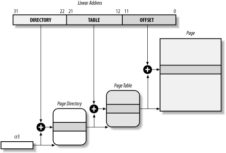
Both the Directory and the Table fields are 10 bits long, so Page Directories and Page Tables can include up to 1,024 entries. It follows that a Page Directory can address up to 1024 × 1024 × 4096=232 memory cells, as you’d expect in 32-bit addresses.
The entries of Page Directories and Page Tables have the same structure. Each entry includes the following fields:
-
Presentflag If it is set, the referred-to page (or Page Table) is contained in main memory; if the flag is 0, the page is not contained in main memory and the remaining entry bits may be used by the operating system for its own purposes. If the entry of a Page Table or Page Directory needed to perform an address translation has the
Presentflag cleared, the paging unit stores the linear address in a control register namedcr2and generates the exception 14: the Page Fault exception. (We shall see in Chapter 16 how Linux uses this field.)- Field containing the 20 most significant bits of a page frame physical address
Since each page frame has a 4-KB capacity, its physical address must be a multiple of 4,096 so the 12 least significant bits of the physical address are always equal to 0. If the field refers to a Page Directory, the page frame contains a Page Table; if it refers to a Page Table, the page frame contains a page of data.
-
Accessedflag Sets each time the paging unit addresses the corresponding page frame. This flag may be used by the operating system when selecting pages to be swapped out. The paging unit never resets this flag; this must be done by the operating system.
-
Dirtyflag Applies only to the Page Table entries. It is set each time a write operation is performed on the page frame. As for the
Accessedflag,Dirtymay be used by the operating system when selecting pages to be swapped out. The paging unit never resets this flag; this must be done by the operating system.-
Read/Writeflag Contains the access right (Read/Write or Read) of the page or of the Page Table (see Section 2.4.3 later in this chapter).
-
User/Supervisorflag Contains the privilege level required to access the page or Page Table (see the later section Section 2.4.3).
-
PCDandPWTflags Controls the way the page or Page Table is handled by the hardware cache (see Section 2.4.7 later in this chapter).
-
Page Sizeflag Applies only to Page Directory entries. If it is set, the entry refers to a 2 MB- or 4 MB-long page frame (see the following sections).
-
Globalflag Applies only to Page Table entries. This flag was introduced in the Pentium Pro to prevent frequently used pages from being flushed from the TLB cache (see Section 2.4.8 later in this chapter). It works only if the Page Global Enable (
PGE) flag of registercr4is set.
Starting with the Pentium model, 80 × 86 microprocessors introduce extended paging , which allows page frames to be 4 MB instead of 4 KB in size (see Figure 2-7).
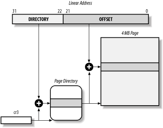
As mentioned in the previous section, extended paging is enabled by
setting the Page
Size flag of a
Page Directory entry. In this case, the paging unit divides the 32
bits of a linear address into two fields:
- Directory
The most significant 10 bits
- Offset
The remaining 22 bits
Page Directory entries for extended paging are the same as for normal paging, except that:
The
Page Sizeflag must be set.Only the 10 most significant bits of the 20-bit physical address field are significant. This is because each physical address is aligned on a 4-MB boundary, so the 22 least significant bits of the address are 0.
Extended paging coexists with regular paging; it is enabled by
setting the PSE flag of the cr4
processor register. Extended paging is used to translate large
contiguous linear address ranges into corresponding physical ones; in
these cases, the kernel can do without intermediate Page Tables and
thus save memory and preserve TLB entries (see Section 2.4.8).
The paging unit uses a different protection scheme from the
segmentation unit. While 80 × 86 processors allow four
possible privilege levels to a segment, only two privilege levels are
associated with pages and Page Tables, because privileges are
controlled by the User/Supervisor flag mentioned
in the earlier section Section 2.4.1. When this flag is 0, the
page can be addressed only when the CPL is less
than 3 (this means, for Linux, when the processor is in Kernel Mode).
When the flag is 1, the page can always be addressed.
Furthermore, instead of the three types of access rights (Read,
Write, and Execute) associated with segments, only two types of
access rights (Read and Write) are associated with pages. If the
Read/Write flag of a Page Directory or Page Table
entry is equal to 0, the corresponding Page Table or page can only be
read; otherwise it can be read and written.
A simple example will help in clarifying how regular paging works.
Let’s assume that the kernel assigns the linear
address space between 0x20000000 and
0x2003ffff to a running process.[13] This space
consists of exactly 64 pages. We don’t care about
the physical addresses of the page frames containing the pages; in
fact, some of them might not even be in main memory. We are
interested only in the remaining fields of the Page Table entries.
Let’s start with the 10 most significant bits of the
linear addresses assigned to the process, which are interpreted as
the Directory field by the paging unit. The addresses start with a 2
followed by zeros, so the 10 bits all have the same value, namely
0x080 or 128 decimal. Thus the Directory field in
all the addresses refers to the 129th entry of the process Page
Directory. The corresponding entry must contain the physical address
of the Page Table assigned to the process (see Figure 2-8). If no other linear addresses are assigned to
the process, all the remaining 1,023 entries of the Page Directory
are filled with zeros.
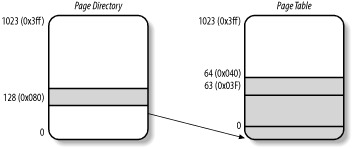
The values assumed by the intermediate 10 bits, (that is, the values
of the Table field) range from 0 to 0x03f, or from
to 63 decimal. Thus, only the first 64 entries of the Page Table are
significant. The remaining 960 entries are filled with zeros.
Suppose that the process needs to read the byte at linear address
0x20021406. This address is handled by the paging
unit as follows:
The Directory field
0x80is used to select entry0x80of the Page Directory, which points to the Page Table associated with the process’s pages.The Table field
0x21is used to select entry0x21of the Page Table, which points to the page frame containing the desired page.Finally, the Offset field
0x406is used to select the byte at offset0x406in the desired page frame.
If the Present flag of the 0x21
entry of the Page Table is cleared, the page is not present in main
memory; in this case, the paging unit issues a Page Fault exception
while translating the linear address. The same exception is issued
whenever the process attempts to access linear addresses outside of
the interval delimited by 0x20000000 and
0x2003ffff since the Page Table entries not
assigned to the process are filled with zeros; in particular, their
Present flags are all cleared.
Two-level paging is used by 32-bit microprocessors. But in recent years, several microprocessors (such as Hewlett-Packard’s Alpha, Intel’s Itanium, and Sun’s UltraSPARC) have adopted a 64-bit architecture. In this case, two-level paging is no longer suitable and it is necessary to move up to three-level paging. Let’s use a thought experiment to explain why.
Start by assuming as large a page size as is reasonable (since you have to account for pages being transferred routinely to and from disk). Let’s choose 16 KB for the page size. Since 1 KB covers a range of 210 addresses, 16 KB covers 214 addresses, so the Offset field is 14 bits. This leaves 50 bits of the linear address to be distributed between the Table and the Directory fields. If we now decide to reserve 25 bits for each of these two fields, this means that both the Page Directory and the Page Tables of each process includes 225 entries — that is, more than 32 million entries.
Even if RAM is getting cheaper and cheaper, we cannot afford to waste so much memory space just for storing the Page Tables.
The solution chosen for the Hewlett-Packard’s Alpha microprocessor — one of the first 64-bit CPUs that appeared on the market — is the following:
Page frames are 8 KB long, so the Offset field is 13 bits long.
Only the least significant 43 bits of an address are used. (The most significant 21 bits are always set to 0.)
Three levels of Page Tables are introduced so that the remaining 30 bits of the address can be split into three 10-bit fields (see Figure 2-11 later in this chapter). Thus, the Page Tables include 210 = 1024 entries as in the two-level paging schema examined previously.
As we shall see in Section 2.5 later in this chapter, Linux’s designers decided to implement a paging model inspired by the Alpha architecture.
The amount of RAM supported by a processor is limited by the number of address pins connected to the address bus. Older Intel processors from the 80386 to the Pentium used 32-bit physical addresses. In theory, up to 4 GB of RAM could be installed on such systems; in practice, due to the linear address space requirements of User Mode processes, the kernel cannot directly address more than 1 GB of RAM, as we shall see in the later section Section 2.5.
However, some demanding applications running on large servers require more than 1 GB of RAM, and in recent years this created a pressure on Intel to expand the amount of RAM supported on the 32-bit 80386 architecture.
Intel has satisfied these requests by increasing the number of address pins on its processors from 32 to 36. Starting with the Pentium Pro, all Intel processors are now able to address up to 236 = 64 GB of RAM. However, the increased range of physical addresses can be exploited only by introducing a new paging mechanism that translates 32-bit linear addresses into 36-bit physical ones.
With the Pentium Pro processor, Intel introduced a mechanism called Physical Address Extension (PAE). Another mechanism, Page Size Extension (PSE-36), was introduced in the Pentium III processor, but Linux does not use it and we won’t discuss it further in this book.
PAE is activated by setting the Physical Address Extension
(PAE) flag in the cr4 control
register. The Page Size (PS) flag in
the page directory entry enables large page sizes
(2 MB when PAE is enabled).
Intel has changed the paging mechanism in order to support PAE.
The 64 GB of RAM are split into 224 distinct page frames, and the physical address field of Page Table entries has been expanded from 20 to 24 bits. Since a PAE Page Table entry must include the 12 flag bits (described in the earlier section Section 2.4.1) and the 24 physical address bits, for a grand total of 36, the Page Table entry size has been doubled from 32 bits to 64 bits. As a result, a 4 KB PAE Page Table includes 512 entries instead of 1,024.
A new level of Page Table called the Page Directory Pointer Table (PDPT) consisting of four 64-bit entries has been introduced.
The
cr3control register contains a 27-bit Page Directory Pointer Table base address field. Since PDPTs are stored in the first 4 GB of RAM and aligned to a multiple of 32 bytes (25), 27 bits are sufficient to represent the base address of such tables.When mapping linear addresses to 4 KB pages (
PSflag cleared in Page Directory entry), the 32 bits of a linear address are interpreted in the following way:-
cr3 Points to a PDPT
- bits 31-30
Point to one of 4 possible entries in PDPT
- bits 29-21
Point to one of 512 possible entries in Page Directory
- bits 20-12
Point to one of 512 possible entries in Page Table
- bits 11-0
Offset of 4 KB page
-
When mapping linear addresses to 2 MB pages (
PSflag set in Page Directory entry), the 32 bits of a linear address are interpreted in the following way:-
cr3 Points to a PDPT
- bits 31-30
Point to one of 4 possible entries in PDPT
- bits 29-21
Point to one of 512 possible entries in Page Directory
- bits 20-0
Offset of 2 MB page
-
To summarize, once cr3 is set, it is possible to
address up to 4 GB of RAM. If we want to address more RAM, we’ll have
to put a new value in cr3 or change the content of
the PDPT. However, the main problem with PAE is that linear addresses
are still 32-bits long. This forces programmers to reuse the same
linear addresses to map different areas of RAM.
We’ll sketch how Linux initializes Page Tables when
PAE is enabled in the later section, Section 2.5.5.4.
Today’s microprocessors have clock rates of several gigahertz, while dynamic RAM (DRAM) chips have access times in the range of hundreds of clock cycles. This means that the CPU may be held back considerably while executing instructions that require fetching operands from RAM and/or storing results into RAM.
Hardware cache memories were introduced to reduce the speed mismatch between CPU and RAM. They are based on the well-known locality principle , which holds both for programs and data structures. This states that because of the cyclic structure of programs and the packing of related data into linear arrays, addresses close to the ones most recently used have a high probability of being used in the near future. It therefore makes sense to introduce a smaller and faster memory that contains the most recently used code and data. For this purpose, a new unit called the line was introduced into the 80 × 86 architecture. It consists of a few dozen contiguous bytes that are transferred in burst mode between the slow DRAM and the fast on-chip static RAM (SRAM) used to implement caches.
The cache is subdivided into subsets of lines. At one extreme, the cache can be direct mapped , in which case a line in main memory is always stored at the exact same location in the cache. At the other extreme, the cache is fully associative , meaning that any line in memory can be stored at any location in the cache. But most caches are to some degree N-way set associative , where any line of main memory can be stored in any one of N lines of the cache. For instance, a line of memory can be stored in two different lines of a two-way set associative cache.
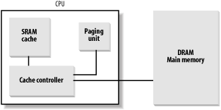
As shown in Figure 2-9, the cache unit is inserted between the paging unit and the main memory. It includes both a hardware cache memory and a cache controller . The cache memory stores the actual lines of memory. The cache controller stores an array of entries, one entry for each line of the cache memory. Each entry includes a tag and a few flags that describe the status of the cache line. The tag consists of some bits that allow the cache controller to recognize the memory location currently mapped by the line. The bits of the memory physical address are usually split into three groups: the most significant ones correspond to the tag, the middle ones to the cache controller subset index, and the least significant ones to the offset within the line.
When accessing a RAM memory cell, the CPU extracts the subset index from the physical address and compares the tags of all lines in the subset with the high-order bits of the physical address. If a line with the same tag as the high-order bits of the address is found, the CPU has a cache hit ; otherwise, it has a cache miss .
When a cache hit occurs, the cache controller behaves differently, depending on the access type. For a read operation, the controller selects the data from the cache line and transfers it into a CPU register; the RAM is not accessed and the CPU saves time, which is why the cache system was invented. For a write operation, the controller may implement one of two basic strategies called write-through and write-back. In a write-through, the controller always writes into both RAM and the cache line, effectively switching off the cache for write operations. In a write-back, which offers more immediate efficiency, only the cache line is updated and the contents of the RAM are left unchanged. After a write-back, of course, the RAM must eventually be updated. The cache controller writes the cache line back into RAM only when the CPU executes an instruction requiring a flush of cache entries or when a FLUSH hardware signal occurs (usually after a cache miss).
When a cache miss occurs, the cache line is written to memory, if necessary, and the correct line is fetched from RAM into the cache entry.
Multiprocessor systems have a separate hardware cache for every processor, and therefore need additional hardware circuitry to synchronize the cache contents. As shown in Figure 2-10, each CPU has its own local hardware cache. But now updating becomes more time consuming: whenever a CPU modifies its hardware cache, it must check whether the same data is contained in the other hardware cache; if so, it must notify the other CPU to update it with the proper value. This activity is often called cache snooping . Luckily, all this is done at the hardware level and is of no concern to the kernel.

Cache technology is rapidly evolving. For example, the first Pentium models included a single on-chip cache called the L1-cache . More recent models also include another larger, slower on-chip cache called the L2-cache . The consistency between the two cache levels is implemented at the hardware level. Linux ignores these hardware details and assumes there is a single cache.
The CD flag of the cr0
processor register is used to enable or disable the cache circuitry.
The NW flag, in the same register, specifies
whether the write-through or the write-back strategy is used for the
caches.
Another interesting feature of the Pentium cache is that it lets an
operating system associate a different cache management policy with
each page frame. For this purpose, each Page Directory and each Page
Table entry includes two flags:
PCD
(Page Cache Disable), which
specifies whether the cache must be enabled or disabled while
accessing data included in the page frame; and
PWT
(Page Write-Through), which specifies
whether the write-back or the write-through strategy must be applied
while writing data into the page frame. Linux clears the
PCD and PWT flags of all Page
Directory and Page Table entries; as a result, caching is enabled for
all page frames and the write-back strategy is always adopted for
writing.
Besides general-purpose hardware caches, 80 × 86 processors include other caches called Translation Lookaside Buffers (TLB) to speed up linear address translation. When a linear address is used for the first time, the corresponding physical address is computed through slow accesses to the Page Tables in RAM. The physical address is then stored in a TLB entry so that further references to the same linear address can be quickly translated.
In a multiprocessor system, each CPU has its own TLB, called the local TLB of the CPU. Contrary to the L1 cache, the corresponding entries of the TLB need not be synchronized because processes running on the existing CPUs may associate the same linear address with different physical ones.
When the cr3 control register of a CPU is
modified, the hardware automatically invalidates all entries of the
local TLB.
[13] As we shall see in the following chapters, the 3 GB linear address space is an upper limit, but a User Mode process is allowed to reference only a subset of it.