
28
CHAPTER
Digital Basics
ENGINEERS AND TECHNICIANS CALL AN ELECTRONIC SIGNAL DIGITAL WHEN IT CAN ATTAIN A LIMITED number of well-defined states. Digital signals contrast with analog signals, which vary over a continuous range and, therefore, can, in theory, attain infinitely many different instantaneous states. Figure 28-1 shows an example of an analog signal (at A) and a digital signal (at B).

28-1 An analog wave (A) and a digital rendition of the same wave (B).
Numeration Systems
In everyday life, most of us deal with the decimal number system, which makes use of digits from the set {0, 1, 2, 3, 4, 5, 6, 7, 8, 9}. Machines, such as computers and communications devices, offer other numeration schemes.
Decimal
The familiar decimal number system is also called base 10 or radix 10. When we express nonnegative integers in this system, we multiply the right-most digit by 100, or 1. We multiply the next digit to the left by 101, or 10. The power of 10 increases as we move to the left. Once we’ve multiplied the digits, we add up all the resulting values. For example:
8 × 100 + 5 × 101 + 0 × 102 + 2 × 10³ + 6 × 10⁴ + 8 × 105
= 862,058
Binary
The binary number system denotes numbers using only the digits 0 and 1. We’ll sometimes hear this system called base 2 or radix 2. When we express nonnegative integers in binary notation, we multiply the rightmost digit by 20, or 1. The next digit to the left is multiplied by 21, or 2. The power of 2 increases as we continue to the left, so we get a “fours” digit, then an “eights” digit, then a “16s” digit, and so on. For example, consider the decimal number 94. In the binary system, we would write this quantity as 1011110. It breaks down into the sum
0 × 20 + 1 × 21 + 1 × 22 + 1 × 23 + 1 × 24 + 0 × 25 + 1 × 26
= 94
Octal
Another scheme, sometimes used in computer programming, goes by the name octal number system because it has eight symbols (according to our way of thinking), or 23. Every digit constitutes an element of the set {0, 1, 2, 3, 4, 5, 6, 7}. Some people call this system base 8 or radix 8. When we express nonnegative integers in octal notation, we multiply the rightmost digit by 80, or 1. The next digit to the left is multiplied by 81, or 8. The power of 8 increases as we continue to the left, so we get a “64s” digit, then a “512s” digit, and so on. For example, we render the decimal quantity 3085 in octal form as 6015. We can break it down into the sum
5 × 80 + 1 × 81 + 0 × 82 + 6 × 83
= 3085
Hexadecimal
Another system used in computer work is the hexadecimal number system. It has 16 (24) symbols: the usual 0 through 9 plus six more, represented by the uppercase English letters A through F, yielding the digit set {0, 1, 2, 3, 4, 5, 6, 7, 8, 9, A, B, C, D, E, F}. This system is sometimes called base 16 or radix 16. All of the hexadecimal digits 0 through 9 represent the same values as their decimal counterparts. However, we have the following additional digits:
• Hexadecimal A equals decimal 10
• Hexadecimal B equals decimal 11
• Hexadecimal C equals decimal 12
• Hexadecimal D equals decimal 13
• Hexadecimal E equals decimal 14
• Hexadecimal F equals decimal 15
When we express nonnegative integers in hexadecimal notation, we multiply the rightmost digit by 160, or 1. We multiply the next digit to the left by 161, or 16. The power of 16 increases as we continue to the left, so we get a “256s” digit, then a “4096s” digit, and so on. For example, we write the decimal quantity 35,898 in hexadecimal form as 8C3A. Remembering that C = 12 and A = 10, we can break the hexadecimal number down into the following sum:
A × 160 + 3 × 161 + C × 162 + 8 × 163
= 35,898
Digital Logic
Digital logic, also called simply logic, is the form of “reasoning” used by electronic machines. Engineers also use the term in reference to the circuits that make up digital devices and systems.
Boolean Algebra
Boolean algebra constitutes a system of logic using the numbers 0 and 1 with the operations AND (multiplication), OR (addition), and NOT (negation). Combinations of these operations give us two more, called NAND (NOT AND) and NOR (NOT OR). This system, which gets its name from the nineteenth-century British mathematician George Boole, plays a vital role in the design of digital electronic circuits.
• The AND operation, also called logical conjunction, operates on two or more quantities. Let’s denote it using an asterisk, for example X * Y.
• The NOT operation, also called logical inversion or logical negation, operates on a single quantity. Let’s denote it using a minus sign (–), for example –X.
• The OR operation, also called logical disjunction, operates on two or more quantities. Let’s denote it using a plus sign (+), for example X + Y.
Table 28-1A breaks down all the possible input and output values for the above-described Boolean operations, where 0 indicates “falsity” and 1 indicates “truth.” In mathematics and philosophy courses involving logic, you can expect to see other symbols used for conjunction and disjunction.
Table 28-1A Boolean Operations

Theorems
Table 28-1B shows several logic equations that hold true under all circumstances, that is, for all values of the logical variables X, Y, and Z. We call such facts theorems. Statements on either side of the equals (=) sign in each case are logically equivalent, meaning that one is true if and only if (iff) the other is true. For example, the statement X = Y means “If X then Y, and if Y then X.” Boolean theorems allow us to simplify complicated logic functions, facilitating the construction of a circuit to perform a specific digital operation using the smallest possible number of switches.
Table 28-1B Common Theorems in Boolean Algebra

Positive versus Negative Logic
In so-called positive logic, a circuit represents the binary digit 1 with an electrical potential of approximately +5 V DC (called the high state or simply high), while the binary digit 0 appears as little or no DC voltage (called the low state or simply low). Some circuits employ negative logic, in which little or no DC voltage (low) represents logic 1, while +5 V DC (high) represents logic 0. In another form of negative logic, the digit 1 appears as a negative voltage (such as –5 V DC, constituting the low state) and the digit 0 appears as little or no DC voltage (the high state because it has the more positive voltage). To avoid confusion, let’s stay with positive logic for the rest of this chapter!
Logic Gates
All digital electronic devices employ switches that perform specific logical operations. These switches, called logic gates, can have anywhere from one to several inputs and (usually) a single output.
• A logical inverter, also called a NOT gate, has one input and one output. It reverses, or inverts, the state of the input. If the input equals 1, then the output equals 0. If the input equals 0, then the output equals 1.
• An OR gate can have two or more inputs (although it usually has only two). If both, or all, of the inputs equal 0, then the output equals 0. If any of the inputs equal 1, then the output equals 1. Mathematical logicians would tell us that such a gate performs an inclusive-OR operation because it “includes” the case where both variables are high.
• An AND gate can have two or more inputs (although it usually has only two). If both, or all, of the inputs equal 1, then the output equals 1. If any of the inputs equal 0, then the output equals 0.
• An OR gate can be followed by a NOT gate. This combination gives us a NOT-OR gate, more often called a NOR gate. If both, or all, of the inputs equal 0, then the output equals 1. If any of the inputs equal 1, then the output equals 0.
• An AND gate can be followed by a NOT gate. This combination gives us a NOT-AND gate, more often called a NAND gate. If both, or all, of the inputs equal 1, then the output equals 0. If any of the inputs equal 0, then the output equals 1.
• An exclusive OR gate, also called an XOR gate, has two inputs and one output. If the two inputs have the same state (either both 1 or both 0), then the output equals 0. If the two inputs have different states, then the output equals 1. Mathematicians use the term exclusive-OR operation because it doesn’t “include” the case where both variables are high.
Table 28-2 summarizes the functions of the above-defined logic gates, assuming a single input for the NOT gate and two inputs for the others. Figure 28-2 illustrates the schematic symbols that engineers and technicians use to represent these gates in circuit diagrams.
Table 28-2 Logic Gates and Their Characteristics

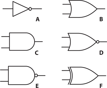
28-2 An inverter or NOT gate (A), an OR gate (B), an AND gate (C), a NOR gate (D), a NAND gate (E), and an XOR gate (F).
Clocks
In electronics, the term clock refers to a circuit that generates pulses at high speed and at precise, constant time intervals. The clock sets the tempo for the operation of digital devices. In a computer, the clock acts like a metronome for the microprocessor. We express or measure clock speeds as frequencies in hertz (Hz). One hertz equals one pulse per second. Higher-frequency units work out as follows, just as they do with analog wave signals:
• A kilohertz (kHz) equals 1000 or 103 pulses per second
• A megahertz (MHz) equals 1,000,000 or 106 pulses per second
• A gigahertz (GHz) equals 1,000,000,000 or 109 pulses per second
• A terahertz (THz) equals 1,000,000,000,000 or 1012 pulses per second
In positive logic, a clock generates brief high pulses at regular intervals. The normal state is low.
Flip-Flops
A flip-flop is a specialized circuit constructed from logic gates, known collectively as a sequential gate. In a sequential gate, the output state depends on both the inputs and the outputs. The term “sequential” comes from the fact that the output depends not only on the states of the circuit at any given instant in time, but also on the states immediately preceding. A flip-flop has two states, called set and reset. Usually, the set state corresponds to logic 1 (high), and the reset state corresponds to logic 0 (low). In schematic diagrams, a flip-flop is usually shown as a rectangle with two or more inputs and two outputs. If the rectangle symbol is used, the letters FF, for “flip-flop,” are printed or written at the top of the rectangle, either inside or outside. Several different types of flip-flop exist, as follows.
• In an R-S flip-flop, the inputs are labeled R (reset) and S (set). Engineers call the outputs Q and –Q. (Often, rather than –Q, we’ll see Q′, or perhaps Q with a line over it.) Table 28-3A shows the input and output states. If R = 0 and S = 0, the output states remain at the values they’ve attained for the moment. If R = 0 and S = 1, then Q = 1 and –Q = 0. If R = 1 and S = 0, then Q = 0 and –Q = 1. When S = 1 and R = 1, the circuit becomes unpredictable.

• In a synchronous flip-flop, the states change when triggered by the signal from an external clock. In static triggering, the outputs change state only when the clock signal is either high or low. This type of circuit is sometimes called a gated flip-flop. In positive-edge triggering, the outputs change state at the instant the clock pulse is positive-going. In negative-edge triggering, the outputs change state at the instant the clock pulse is negative-going. The abrupt rise or fall of a pulse looks like the edge of a cliff (Fig. 28-3).

28-3 Digital pulse edges are either positive-going (abruptly increasing in the positive sense) or negative-going (abruptly increasing in the negative sense).
• In a master/slave (M/S) flip-flop, the inputs are stored before the outputs can change state. This device comprises essentially two R-S flip-flops in series. We call the first flip-flop the master and the second flip-flop the slave. The master functions when the clock output is high, and the slave acts during the next ensuing low portion of the clock output. The time delay prevents confusion between the input and output.
• The operation of a J-K flip-flop resembles the functioning of an R-S flip-flop, except that the J-K device has a predictable output when the inputs both equal 1. Table 28-3B shows the input and output states for this type of flip-flop. The output changes only when a triggering pulse is received.
• The operation of an R-S-T flip-flop resembles that of an R-S flip-flop, except that a high pulse at an additional T input causes the circuit to change state.
• A circuit called a T flip-flop has only one input. Each time a high pulse appears at the input, the output reverses its state, either from 1 to 0 or else from 0 to 1. Note the difference between this type of circuit and a simple inverter (NOT gate)!
Counters
A counter literally counts digital pulses one by one. Each time the counter receives a high pulse, the binary number in its memory increases by 1. A frequency counter can measure the frequency of an AC wave or signal by tallying up the cycles over a precisely known period of time. The circuit consists of a gate, which begins and ends each counting cycle at defined intervals. (Don’t confuse this type of gate with the logic gates described a few moments ago.) The counter’s accuracy depends on the gate time, or how long the gate remains open to accept pulses for counting. As we increase the gate time in a frequency counter, the accuracy improves. Although the counter tallies up the pulses as binary numbers, the display shows base-10 digital numerals.
Binary Communications
If we want to attain multilevel signaling (digital transmission with more than two states), we can represent each different signal level with a unique group of binary digits, representing a specific binary number. A group of three binary digits can represent up to 23, or eight, levels. A group of four binary digits can represent up to 24, or 16, levels. The term “binary digit” is commonly contracted to bit. A bit is represented by either logic 0 or logic 1. Some engineers call a group of eight bits an octet, and in many systems an octet corresponds to a unit called a byte.
Forms of Binary Signaling
Engineers have invented numerous forms, or modes, of binary communication. Three classical examples follow.
1. Morse code is the oldest binary mode. The logic states are called mark (key-closed or on) and space (key-open or off). Morse code is obsolete in modern systems, but amateur radio operators consider it a backup mode that can work in case digital signal-reading machines fail.
2. Baudot, also called the Murray code, is a five-unit digital code not widely used by today’s digital equipment, except in a few antiquated teleprinter systems. There exist 25, or 32, possible representations.
3. The American National Standard Code for Information Interchange (ASCII) is a seven-unit code for the transmission of text and simple computer programs. There exist 27, or 128, possible representations.
Bits
We can represent large quantities of data according to powers of 2 or according to powers of 10. This duality can cause some confusion. Here’s how the units build up when we talk about bits:
• A kilobit (kb) equals 103 or 1000 bits
• A megabit (Mb) equals 106 or 1,000,000 bits
• A gigabit (Gb) equals 109 or 1,000,000,000 bits
• A terabit (Tb) equals 1012 bits or 1000 Gb
• A petabit (Pb) equals 1015 bits or 1000 Tb
• An exabit (Eb) equals 1018 bits or 1000 Pb
We use power-of-10 multiples of bits per second (bps, kbps, Mbps, Gbps, and so on) to express data speed when we transmit digital signals from one location (called the source) to another location (called the destination).
Bytes
Data quantity in storage or memory (residing in a fixed location rather than propagating from one place to another) is specified in units that comprise power-of-2 multiples of bytes. Here’s how the units build up:
• A kilobyte (KB) equals 210 or 1024 bytes
• A megabyte (MB) equals 220 or 1,048,576 bytes
• A gigabyte (GB) equals 230 or 1,073,741,824 bytes
• A terabyte (TB) equals 240 bytes or 1024 GB
• A petabyte (PB) equals 250 bytes or 1024 TB
• An exabyte (EB) equals 260 bytes or 1024 PB
Note also the following conventions concerning abbreviations for the units and prefix multipliers:
• The lowercase b stands for “bits.”
• The uppercase B stands for “bytes.”
• The lowercase k stands for 103 or 1000.
• The uppercase K stands for 210 or 1024.
• We always denote the prefix multipliers M, G, T, P, and E in uppercase.
Baud
The term baud refers to the number of times per second that a signal changes state. We’ll read about baud (sometimes called baud rate) only in texts and papers dated before about 1980. Bits per second (bps) and baud represent qualitatively different parameters, even though they might come out quantitatively close to each other for a particular digital signal. Some engineers used to speak and write about bps and baud as if they meant the same thing. They don’t!
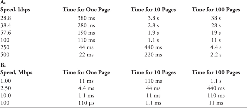
Examples of Data Speed
When we link multiple computers in a network, each computer has a modem (modulator/demodulator) connecting it to the communications medium. The slowest modem determines the speed at which the machines communicate. Table 28-4 shows common data speeds and the approximate time periods required to send one page, 10 pages, and 100 pages of double-spaced, typewritten text at each speed.
Table 28-4 Time Needed to Send Data at Various Speeds
Abbreviations: s = second, ms = millisecond (0.001 s), μs = microsecond (0.000001 s)
Data Conversion
We can convert an analog signal into a string of pulses whose amplitudes have a finite number of states, usually some power of 2. This scheme constitutes analog-to-digital (A/D) conversion; the reverse of digital-to-analog (D/A) conversion.
Figure 28-4 shows the functional difference between analog and digital signals. Imagine sampling the curve to obtain a sequence, or train, of pulses (A/D conversion), or smoothing out the pulses to obtain the curve (D/A conversion).

28-4 An analog waveform (dashed curve) and an 8-level digital representation of the same curve (vertical bars).
We can transmit and receive binary data one bit at a time along a single line or channel. This mode constitutes serial data transmission. Higher data speeds can be obtained by using multiple lines or a wideband channel, sending independent sequences of bits along each line or subchannel. Then we have parallel data transmission.
Parallel-to-serial (P/S) conversion involves the reception of bits from multiple lines or channels, and their retransmission one by one along a single line or channel. A buffer stores the bits from the parallel lines or channels while they await transmission along the serial line or channel. Serial-to-parallel (S/P) conversion involves the reception of bits one by one from a serial line or channel, and their retransmission in batches along several lines or channels. The output of an S/P converter cannot go any faster than the input, but we can find such a system useful when we want to interface between a serial-data device and a parallel-data device.
Figure 28-5 illustrates a circuit that employs a P/S converter at the source and an S/P converter at the destination. In this example, the words comprise eight-bit bytes. However, the words could have 16, 32, 64, or even 128 bits, depending on the communications scheme.

28-5 A communications circuit employing parallel-to-serial (P/S) conversion at the source and serial-to-parallel (S/P) conversion at the destination.
Data Compression
Data compression provides us with a way to maximize the amount of digital information that a machine can store in a given space, or that we can send within a certain period of time.
Text files can be compressed by replacing often-used words and phrases with symbols such as =, #, &, $, and @, as long as none of these symbols occurs in the uncompressed file. As the data is received, the machine can decompress it by substituting the original words and phrases for the symbols.
Digital image files can be compressed in either of two ways. In lossless image compression, detail is not sacrificed; only the redundant bits are eliminated. In lossy image compression, we lose some detail, although the loss is rarely severe enough to degrade the quality of the image to an objectionable extent.
Packet Wireless
In packet wireless, we connect a computer to a radio transceiver using a terminal node controller (TNC), which resembles a computer modem. Figure 28-6A shows an example. The computer has a modem as well as a TNC, so we can send and receive messages using conventional online services as well as radio.

28-6 At A, a packet-wireless station. At B, passage of a packet through nodes in a wireless communications circuit.
Figure 28-6B shows how a packet-wireless message is routed. Black dots represent subscribers. Rectangles represent local nodes, each of which serves subscribers by means of short-range links at very-high, ultra-high, or microwave radio frequencies. The nodes are interconnected by terrestrial radio links if they are relatively near each other. If the nodes are widely separated, satellite links interconnect them.
Digital Signal Processing
Digital signal processing (DSP), a method of improving the precision of digital data, was originally used with radio and television receivers to produce a clear voice and/or picture from a marginal signal. Amateur radio operators did some of the earliest experiments with DSP. In analog modes, such as voice or video, the signals are first changed into digital form by A/D conversion. Then the digital data is “tidied up” so that the pulse timing and amplitude adhere strictly to the protocol (set of standards) for the type of digital data in use. Noise is greatly reduced or eliminated. Finally, the digital signal is changed back to the original voice or video by a D/A converter.
Digital signal processing can extend the workable range of almost any communications circuit because it allows reception under worse conditions than would be possible without it. Digital signal processing also improves the quality of marginal signals, so the receiving equipment or operator makes fewer errors. In circuits that use only digital modes, A/D and D/A conversion aren’t required, but DSP can nevertheless “clean up” the signal, thereby improving the accuracy of the system and making it possible to copy data over and over many times (produce multi-generation copies).
Digital signals have discrete, well-defined states. A machine finds it easier to process a digital signal than to process an analog signal, which has a theoretically infinite number of possible states. In particular, digital signals have well-defined patterns that are easy for computers and microprocessors to recognize and clarify. Binary (two-state) signals are the simplest for machines to work with.
Even the most sophisticated digital computers can’t deal directly with the complex curves of an analog function. Although the modulation envelope of a single-sideband (SSB) signal isn’t difficult for an analog communications receiver to process, a digital machine sees such a waveform as an “alien code.” When we convert analog data to binary digital format, a sophisticated digital electronic circuit can understand it and modify it. The most powerful mainstream microprocessors comprise binary digital devices.
The DSP circuit works by eliminating confusion between digital states. Figure 28-7A shows a hypothetical signal before DSP. Figure 28-7B shows the same signal after DSP. The electronic circuit makes its digital “decision” (high or low) for defined time intervals. If the incoming signal remains above a certain level for an interval of time, the DSP output equals logic 1 (the high state). If the level remains below the critical point for a time interval, then the output equals logic 0 (the low state). A sudden burst of noise, such as sferics (atmospheric “static”) from a nearby thunderstorm, might fool a DSP circuit into thinking that a signal is high when it’s really low. But overall, errors occur less often with DSP than without it.

28-7 At A, a “dirty” binary signal before digital signal processing (DSP). At B, the same signal after DSP.
Quiz
Refer to the text in this chapter if necessary. A good score is at least 18 correct. Answers are in the back of the book.
1. In Boolean algebra, we represent the inclusive logic OR operation as
(a) multiplication.
(b) division.
(c) addition.
(d) subtraction.
2. The hexadecimal numeral C7 represents the same quantity as the decimal numeral
(a) 127.
(b) 199.
(c) 212.
(d) 263.
3. Suppose that we place a NOT gate in cascade (that is, in series) with each of the two inputs X and Y of an AND gate, as shown in Fig. 28-8. If X = 1 and Y = 0, how can we describe the states of the signals at points P and Q?

28-8 Illustration for Quiz Questions 3 and 4.
(a) P = 1 and Q = 1
(b) P = 0 and Q = 1
(c) P = 1 and Q = 0
(d) P = 0 and Q = 0
4. In the situation of Fig. 28-8, under what input conditions will we get logic 1 at the output point R?
(a) X = 1 and Y = 1
(b) X = 0 and Y = 1
(c) X = 1 and Y = 0
(d) X = 0 and Y = 0
5. The binary numeral 10101 represents the same quantity as the decimal numeral
(a) 18.
(b) 21.
(d) 57.
6. The octal numeral 425 represents the same quantity as the decimal numeral
(a) 1034.
(b) 517.
(c) 277.
(d) 194.
7. The decimal numeral 104 translates into the octal numeral
(a) 173.
(b) 161.
(c) 150.
(d) 137.
8. Suppose that we place a NOT gate at the output of an XOR gate, as shown in Fig. 28-9, and then we operate the combination of gates as a “black box.” Under what input conditions X and Y will we get a low state at the output point Q?

28-9 Illustration for Quiz Questions 8 and 9.
(a) Only when X = 0 and Y = 0
(b) Only when X = 1 and Y = 1
(c) Whenever X = Y (X and Y have the same state)
(d) Whenever X ≠ Y (X and Y have opposite states)
9. Under what input conditions X and Y will we get a high state at the output point Q in the “black box” of Fig. 28-9?
(a) Only when X = 0 and Y = 0
(b) Only when X = 1 and Y = 1
(c) Whenever X = Y
(d) Whenever X ≠ Y
10. The second digit from the left in an eight-digit binary numeral carries a decimal value equal to a multiple of
(a) 64.
(b) 128.
(c) 256.
(d) 512.
11. The decimal numeral 35 translates into the hexadecimal numeral
(a) B2.
(b) 2A.
(c) AB.
(d) 23.
12. When both inputs of an R-S flip-flop are high, the output states are
(a) unpredictable.
(b) both high.
(c) both low.
(d) opposite.
13. Suppose that we place a NOT gate in cascade with each of the two inputs X and Y of an XOR gate, as shown in Fig. 28-10. Under what input conditions will we get logic 1 at the output point R?

28-10 Illustration for Quiz Questions 13 and 14.
(a) Only when X = 1 and Y = 1
(b) Only when X = 0 and Y = 0
(c) Whenever X = Y
(d) Whenever X ≠ Y
14. In the circuit of Fig. 28-10, under what input conditions will we get logic 0 at the output point R?
(a) Only when X = 1 and Y = 1
(b) Only when X = 0 and Y = 0
(c) Whenever X = Y
(d) Whenever X ≠ Y
15. In the hexadecimal numeration system, what follows 999?
(a) 1000
(b) 99A
(c) A000
(d) A99
16. Digital signal processing can
(a) enhance the distinction between high and low logic states.
(b) minimize the number of errors per unit of time in a digital communications system.
(c) allow us to make accurate multigenerational copies of digital data.
(d) All of the above
17. The largest decimal value that we can represent as an eight-digit binary numeral is
(a) 511.
(b) 255.
(c) 127.
(d) 63.
18. To maximize the amount of useful information conveyed in a given time without increasing the actual number of characters or symbols sent, we can employ
(a) D/A conversion.
(b) A/D conversion.
(c) data compression.
(d) data acceleration.
19. If both of the inputs to a two-input NAND gate equal logic 0, the output state is
(a) low.
(b) high.
(c) unpredictable and unstable.
(d) a function of the previous states.
20. What do we call the number of times per second that a digital signal changes from high to low or vice versa?
(a) Baud
(b) Bits per second
(c) Characters per second
(d) Conversion rate