
26
CHAPTER
Amplifiers and Oscillators
NOW THAT WE KNOW HOW TRANSISTORS WORK, WE’RE READY TO LEARN ABOUT AMPLIFIERS AND oscillators that use these devices. But first, let’s take a closer look at a topic that we’ve encountered briefly already: the decibel (dB) as an expression of relative signal strength.
The Decibel Revisited
We can consider amplitude increases as positive gain and amplitude decreases as negative gain. For example, if a circuit’s output signal amplitude equals +6 dB relative to the input signal amplitude, then the output exceeds the input. If the output signal amplitude is −14 dB relative to the input, then the output is weaker than the input. In the first case, we say that the circuit has a gain of 6 dB. In the second case, we say that the circuit has a gain of −14 dB or a loss of 14 dB.
For Voltage
Consider a circuit with an RMS AC input voltage of Ein and an RMS AC output voltage of Eout, with both voltages expressed in the same units (volts, millivolts, microvolts, or whatever). Also suppose that the input and output impedances both constitute pure resistances of the same ohmic value. We can calculate the voltage gain of the circuit, in decibels, with the formula
Gain (dB) = 20 log (Eout/Ein)
In this equation, “log” stands for the base-10 logarithm or common logarithm. Scientists and engineers write the base-10 logarithm of a quantity x as “log x” or sometimes as “log10 x.” We can consider the coefficient 20 in the above equation to be an exact value when we make calculations, no matter how many significant digits we need.
Logarithms can have other bases besides 10, the most common of which is the exponential constant, symbolized as e and equal to approximately 2.71828. Scientists and engineers express the base-e logarithm (also called the natural logarithm) of a quantity x as “loge x” or “ln x.” Without knowing all of the mathematical particulars concerning how logarithmic functions behave, we can calculate the logarithms of specific numbers with the help of a good scientific calculator. From now on, let’s agree that when we say “logarithm” or write “log,” we mean the base-10 logarithm.
Suppose that a circuit has an RMS AC input of 1.00 V and an RMS AC output of 14.0 V. How much gain, in decibels, does this circuit produce?
Solution
First, you must find the ratio Eout/Ein. Because Eout = 14. 0 V RMS and Ein = 1.00 V RMS, the ratio equals 14.0/1.00, or 14.0. Next, find the logarithm of 14.0. A calculator tells you that this quantity is quite close to 1.146128036. Finally, multiply this number by 20 and then round off to three significant figures, getting 22.9 dB.
Problem 26-2
Suppose that a circuit has an RMS AC input voltage of 24.2 V and an RMS AC output voltage of 19.9 V. What’s the gain in decibels?
Solution
Find the ratio Eout/Ein = 19.9/24.2 = 0.822314…. (The sequence of three dots, called an ellipsis, indicates extra digits introduced by the calculator. You can leave them in until the final roundoff.) When you use a calculator to find the logarithm of this quantity, you get log 0.822314… = −0.0849622…. The gain equals 20 × (−0.0849622), which rounds off to −1.70 dB.
For Current
We can calculate current gain or loss figures in decibels in the same way as we calculate voltage gain or loss figures. If Iin represents the RMS AC input current and Iout represents the RMS AC output current (in the same units as Iin, such as amperes, milliamperes, microamperes, or whatever), then
Gain (dB) = 20 log (Iout/Iin)
For this formula to work, the input and output impedances must both comprise pure resistances, and the ohmic values must be identical.
For Power
We can calculate the power gain of a circuit, in decibels, by cutting the coefficient of the formula in half, from exactly 20 to exactly 10, accurate to as many significant digits as we want. If Pin represents the input signal power and Pout represents the output signal power (in the same units as Pin, such as watts, milliwatts, microwatts, kilowatts, or whatever), then
Gain (dB) = 10 log (Pout/Pin)
For this formula to work, the input and output impedances should both show up as pure resistances, but their ohmic values can differ.
Problem 26-3
Suppose that a power amplifier has an input of 5.72 W and an output of 125 W. What’s the gain in decibels?
Find the ratio Pout/Pin = 125/5.72 = 21.853146…. Then find the logarithm, obtaining log 21.853146… = 1.339513…. Finally, multiply by 10 and round off to obtain a gain figure of 10 ×1.339513… = 13.4 dB.
Problem 26-4
Suppose that an attenuator (a circuit designed deliberately to produce power loss) provides 10 dB power reduction. You supply this circuit with an input signal at 94 W. What’s the output power?
Solution
An attenuation of 10 dB represents a gain of −10 dB. You know that Pin = 94 W, so Pout constitutes the unknown in the power gain formula. You must, therefore, solve for Pout in the equation
−10 = 10 log (Pout/94)
First, divide each side by 10, getting
−1 = log (Pout/94)
To solve this equation, you must take the base-10 antilogarithm, also known as the antilog or inverse log, of each side. The antilog function “undoes” the work of the log function. The antilog of a value x can be abbreviated as “antilog x.” Pure mathematicians, as well as some scientists and engineers, denote it as “log−1 x.” Antilogarithms of specific numbers, like logarithms, can be determined with any good scientific calculator. (Function keys for the antilogarithm vary, depending on the particular calculator you use. You might have to enter the value and then hit an “Inv” key followed by a “log” key; you might enter the value and then hit a “10x” key.) When you take the antilogarithm of both sides of the above equation, you get
antilog (−1) = antilog [log (Pout/94)]
Working out the value on the left-hand side with a calculator, and noting on the right-hand side that the antilog “undoes” the work of the log, you get
0.1 = Pout/94
Multiplying each side by 94 tells you that
94 × 0.1 = Pout
Finally, when you multiply out the left-hand side and transpose the left-hand and right-hand sides of the equation, you get the answer as
Pout = 9.4 W
Decibels and Impedance
When determining the voltage gain (or loss) and the current gain (or loss) for a circuit in decibels, you can expect to get the same figure for both parameters only when the complex input impedance is identical to the complex output impedance. If the input and output impedances differ (either reactance-wise or resistance-wise, or both), then the voltage gain or loss generally differs from the current gain or loss.
Consider how transformers work. A step-up transformer, in theory, has voltage gain, but this voltage increase alone doesn’t make a signal more powerful. A step-down transformer can exhibit theoretical current gain, but again, this current increase alone doesn’t make a signal more powerful. In order to make a signal more powerful, a circuit must increase the signal power—the product of the voltage and the current!
When determining power gain (or loss) for a particular circuit in decibels, the input and output impedances do not matter, as long as they’re both free of reactance. In this sense, positive power gain always represents a real-world increase in signal strength. Similarly, negative power gain (or power loss) always represents a true decrease in signal strength.
Whenever we want to work out decibel values for voltage, current, or power, we should strive to get rid of all the reactance in a circuit, so that our impedances constitute pure resistances. Reactance “artificially” increases or decreases current and voltage levels; and while reactance theoretically consumes no power, it can have a profound effect on the behavior of instruments that measure power, and it can cause power to go to waste as unwanted heat dissipation.
Basic Bipolar-Transistor Amplifier
In the previous chapters, you saw some circuits that use transistors. We can apply an input signal to some control point (the base, gate, emitter, or source), causing a much greater signal to appear at the output (usually the collector or drain). Figure 26-1 shows a circuit in which we’ve wired up an NPN bipolar transistor to serve as a common-emitter amplifier. The input signal passes through C2 to the base. Resistors R2 and R3 provide the base bias. Resistor R1 and capacitor C1 allow for the emitter to maintain a constant DC voltage relative to ground, while keeping it grounded for the AC signal. Resistor R1 also limits the current through the transistor. The AC output signal goes through capacitor C3. Resistor R4 keeps the AC output signal from shorting through the power supply.

26-1 A generic amplifier circuit with a bipolar transistor.
In this amplifier, the optimum capacitance values depend on the design frequency of the amplifier, and also on the impedances at the input and output. In general, as the frequency and/or circuit impedance increase, we need less capacitance. At audio frequencies (abbreviated AF and representing frequencies from approximately 20 Hz to 20 kHz) and low impedances, the capacitors might have values as large as 100 μF. At radio frequencies (RF) and high impedances, values will normally equal only a fraction of a microfarad, down to picofarads at the highest frequencies and impedances. The optimum resistor values also depend on the application. In the case of a weak-signal amplifier, typical values are 470 ohms for R1, 4.7 k for R2,10 k for R3, and 4.7 k for R4.
Basic FET Amplifier
Figure 26-2 shows an N-channel JFET hooked up as a common-source amplifier. The input signal passes through C2 to the gate. Resistor R2 provides the gate bias. Resistor R1 and capacitor C1 give the source a DC voltage relative to ground, while grounding it for signals. The output signal goes through C3. Resistor R3 keeps the output signal from shorting through the power supply.

26-2 A generic amplifier circuit with a JFET.
A JFET exhibits high input impedance, so the value of C2 should be small. If we use a MOSFET rather than a JFET, we’ll get a higher input impedance, so C2 will be smaller yet, sometimes 1 pF or less. The resistor values depend on the application. In some instances, we won’t need R1 and C1 at all, and we can connect the source directly to ground. If we use resistor R1, its optimum value depends on the input impedance and the bias needed for the FET. For a weak-signal amplifier, typical values are 680 ohms for R1, 10 k for R2, and 100 ohms for R3.
Amplifier Classes
Engineers classify analog amplifier circuits according to the bias arrangement as class A, class AB, class B, and class C. Each class has its own special characteristics, and works best in its own unique set of circumstances. A specialized amplifier type, called class D, can also be used in certain situations.
The Class-A Amplifier
With the previously mentioned component values, the amplifier circuits in Figs. 26-1 and 26-2 operate in the class-A mode. This type of amplifier is linear, meaning that the output waveform has the same shape as (although a greater amplitude than) the input waveform.
When we want to obtain class-A operation with a bipolar transistor, we must bias the device so that, with no signal input, it operates near the middle of the straight-line portion of the IC versus IB (collector current versus base current) curve. Figure 26-3 shows this situation for a bipolar transistor. With a JFET or MOSFET, the bias must be such that, with no signal input, the device operates near the middle of the straight-line part of the ID versus EG (drain current versus gate voltage) curve as shown in Fig. 26-4.

26-3 Classes of amplifier operation for a typical bipolar transistor.

26-4 Classes of amplifier operation for a typical JFET.
When we use a class-A amplifier in the “real world,” we must never allow the input signal to get too strong. An excessively strong input signal will drive the device out of the straight-line part of the characteristic curve during part of the cycle. When this phenomenon occurs, the output waveform will no longer represent a faithful reproduction of the input waveform, and the amplifier will become nonlinear. In some types of amplifiers, we can tolerate (or even encourage) nonlinearity, but we’ll want a class-A amplifier to operate in a linear fashion at all times.
Class-A amplifiers suffer from one outstanding limitation: The transistor draws current whether or not any input signal exists. The transistor must “work hard” even when no signal comes in. For weak-signal applications, the “extra work load” doesn’t matter much; we must concern ourselves entirely with getting plenty of gain out of the circuit.
The Class-AB Amplifier
When we bias a bipolar transistor close to cutoff under no-signal conditions, or when we bias a JFET or MOSFET near pinchoff, the input signal always drives the device into the nonlinear part of the operating curve. (Figures 26-3 and 26-4 are examples of operating curves.) Then, by definition, we have a class-AB amplifier. Figures 26-3 and 26-4 show typical bias zones for class-AB amplifier operation. A small collector or drain current flows when no input signal exists, but it’s less than the no-signal current in a class-A amplifier.
Engineers sometimes specify two distinct modes of class-AB amplification. If the bipolar transistor or FET never goes into cutoff or pinchoff during any part of the input signal cycle, the amplifier works in class AB1. If the device goes into cutoff or pinchoff for any part of the cycle (up to almost half), the amplifier operates in class AB2.
In a class-AB amplifier, the output-signal wave doesn’t have the same shape as the input-signal wave. But if the signal wave is modulated, such as in a voice radio transmitter, the waveform of the modulating signal comes out undistorted anyway. Therefore, class-AB operation can work very well for RF power amplifiers.
The Class-B Amplifier
When we bias a bipolar transistor exactly at cutoff or an FET exactly at pinchoff under zero-input-signal conditions, we cause an amplifier to function in the class-B mode. The operating points for class-B operation are labeled on the curves in Figs. 26-3 and 26-4. This scheme, like the class-AB mode, lends itself well to RF power amplification.
In class-B operation, no collector or drain current flows under no-signal conditions. Therefore, the circuit does not consume significant power unless a signal goes into it. (Class-A and class-AB amplifiers consume some DC power under no-signal conditions.) When we provide an input signal, current flows in the device during half of the cycle. The output signal waveform differs greatly from the input waveform. In fact, the wave comes out “half-wave rectified” as well as amplified.
You’ll sometimes hear of class-AB or class-B “linear amplifiers,” especially when you converse with amateur (ham) radio operators. In this context, the term “linear” refers to the fact that the amplifier doesn’t distort the modulation waveform (sometimes called the modulation envelope), even though the carrier waveform is distorted because the transistor is not biased in the straight-line part of the operating curve under no-signal conditions.
Class-AB2 and class-B amplifiers draw power from the input signal source. Engineers say that such amplifiers require a certain amount of drive or driving power to function. Class-A and class-AB1 amplifiers theoretically need no driving power, although the input signal must provide a certain amount of voltage to influence the behavior of the transistor.
The Class-B Push-Pull Amplifier
We can connect two bipolar transistors or FETs in a pair of class-B circuits that operate in tandem, one for the positive half of the input wave cycle and the other for the negative half. In this way, we can get rid of waveform distortion while retaining all the benefits of class-B operation. We call this type of circuit a class-B push-pull amplifier. Figure 26-5 shows an example using two NPN bipolar transistors.

26-5 A class-B push-pull amplifier using NPN bipolar transistors.
Resistor R1 limits the current through the transistors. Capacitor C1 keeps the input transformer center tap at signal ground, while allowing for some DC base bias. Resistors R2 and R3 bias the transistors precisely at their cutoff points. For best results, the two transistors must be identical. Not only should their part numbers match, but we should pick them out by experiment for each amplifier circuit that we build, to ensure that the characteristics coincide as closely as possible.
Class-B push-pull circuits provide a popular arrangement for audio-frequency (AF) power amplification. Push-pull design offers the easy transistor workload of the class-B mode with the low-distortion, linear amplification characteristics of the class-A mode. However, a push-pull amplifier needs two center-tapped transformers, one at the input and the other at the output, a requirement that makes push-pull amplifiers more bulky and expensive than other types.
All push-pull amplifiers share a unique and interesting quality: They “cancel out” the even-numbered harmonics in the output. This property offers an advantage in the design and operation of wireless transmitters because it gets rid of concerns about the second harmonic, which usually causes more trouble than any other harmonic. A push-pull circuit doesn’t suppress odd-numbered harmonics any more than a “single-ended” circuit (one that employs a single bipolar transistor or FET) does.
The Class-C Amplifier
We can bias a bipolar transistor or FET past cutoff or pinchoff, and it will still work as a power amplifier (PA), provided that the drive is sufficient to overcome the bias during part of the cycle. We call this mode class-C operation. Figures 26-3 and 26-4 show no-signal bias points for class-C amplification.
Class-C amplifiers are nonlinear, even for amplitude-modulation (AM) envelopes. Therefore, engineers generally use class-C circuits only with input signals that are either “full-on” or “full-off.” Such signals include old-fashioned Morse code, along with digital modulation schemes in which the frequency or phase (but not the amplitude) of the signal can vary, but the amplitude is always either zero or maximum.
A class-C amplifier needs a lot of driving power. It does not produce as much gain as other amplification modes. For example, we might need 300 W of signal drive to get 1 kW of signal power output from a class-C power amplifier. However, we get more “signal bang for the buck” in class C than we do with an amplifier working in any other mode. That is to say, we get optimum efficiency from the class-C scheme.
The Class-D Amplifier
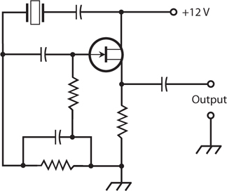
A class-D amplifier differs radically from traditional amplifiers; its output transistors (generally MOSFETs) act in a digital way, always either on or off, as opposed to analog modes for the other classes. Class-D amplifiers use pulse-width modulation (PWM), which you’ll learn about in Chap. 27 (Wireless Transmitters and Receivers) and Chap. 29 (Microcontrollers). Figure 26-6 shows the principle of class-D operation.

26-6 Functional diagram of a class-D audio amplifier.
A class-D amplifier uses a comparator, which you learned about in Chap. 23 (Integrated Circuits) and a triangular-wave oscillator to convert an analog input signal to a train of pulses having different lengths. The pulse length varies in proportion to the instantaneous input-signal voltage. These pulses get amplified by a class-C-like push-pull stage. Then a lowpass filter, playing the role of a digital-to-analog converter, transforms the pulses back into an analog signal. (For low-quality audio applications with a loudspeaker output, the speaker can’t respond fast enough to follow the pulse frequency, so it converts the digital signal to analog form without the need for a separate lowpass filter.)
To visualize the digitization process, imagine the input signal slowly changing compared to the output of the triangular-wave oscillator. Let’s say that the input signal is, at first, stronger than the signal from the triangular-wave oscillator, so the comparator output is high. At some point, the input signal gets weaker than the triangular signal, and the comparator output goes low. The time that this transition takes depends on the voltage of the input signal. The higher the voltage, the longer the pulse. The proportion of the time that the pulse remains high is called the duty cycle. The higher the duty cycle, the stronger the output signal.
When built with MOSFETs that have input impedances on the order of a few megohms, a class-D amplifier can supply several tens of watts of power without overheating. Class-D amplifiers almost always use ICs rather than discrete components, and have largely replaced analog amplifiers in consumer devices, such as cell phones, notebook computers, and tablet computers.
On the downside, class-D amplifiers cause some distortion. For hi-fi audio amplification, therefore, analog designs remain superior; class-A amplifiers are ideal for that purpose.
Efficiency in Power Amplifiers
An efficient power amplifier not only provides optimum output power with minimum heat generation and minimum strain on the transistors, but it conserves energy as well. These factors translate into reduced cost, reduced size and weight, and longer equipment life as compared with inefficient power amplifiers.
The DC Input Power
Suppose that you connect an ammeter or milliammeter in series with the collector or drain of an amplifier and the power supply. While the amplifier operates, the meter will show a certain reading. The reading might appear constant, or it might fluctuate with changes in the input signal level. The DC collector input power to a bipolar-transistor amplifier circuit equals the product of the collector current IC and the collector voltage EC. Similarly, for an FET, the DC drain input power equals the product of the drain current ID and the drain voltage ED. We can categorize DC input power figures as average or peak values. The following discussion involves only average power.
We can observe significant DC collector or drain input power even when an amplifier receives no input signal. A class-A circuit operates this way. In fact, when we apply an input signal to a class-A amplifier, the average DC collector or drain input power does not change compared to the value under no-signal conditions! In class AB1 or class AB2, we observe low current (and, therefore, low DC collector or drain input power) with zero input signal, and higher current (and, therefore, higher DC input power) when we apply a signal to the input. In classes B and C, we see no current (and, therefore, zero DC collector or drain input power) when no input signal exists. The current, and therefore, the DC input power, increase with increasing signal input.
We usually express or measure the DC collector or drain input power in watts, the product of amperes and volts, as long as the circuit has no reactance. We can express it in milliwatts for low-power amplifiers, or kilowatts (and, in extreme cases, megawatts) for high-power amplifiers.
The Signal Output Power
If we want to accurately determine the signal output power from an amplifier, we must employ a specialized AC wattmeter. The design of AF and RF wattmeters represents a sophisticated specialty in engineering. We can’t connect an ordinary DC meter and rectifier diode to a power amplifier’s output terminals and expect to get a true indication of the signal output power.
When a properly operating power amplifier receives no input signal, we never see any signal output, and therefore, the power output equals zero. This situation holds true for all classes of amplification. As we increase the strength of the input signal, we observe increasing signal output power up to a certain point. If we keep increasing the strength of the input signal (that is, the drive) past this point, we see little or no further increase in the signal output power.
We express or measure signal output power in watts, just as we do with DC input power. For very low-power circuits, we might want to specify the signal output power in milliwatts; for moderate- and high-power circuits we can express it in watts, kilowatts, or even megawatts.
Definition of Efficiency
Engineers define the efficiency of a power amplifier as the ratio of the signal output power to the DC input power. We can render this quantity either as a plain fraction (in which case it has a value between 0 and 1) or as a percentage (in which case it has a value between 0% and 100%). Let Pin represent the DC input power to a power amplifier. Let Pout represent the signal output power. We can quantify the efficiency (eff) as the ratio
eff = Pout/Pin
or as the percentage
eff% = 100 Pout/Pin
Problem 26-5
Suppose that a bipolar-transistor amplifier has a DC input power of 120 W and a signal output power of 84 W. What’s the efficiency in percent?
Solution
We should use the formula for amplifier efficiency eff% expressed as a percentage. When we go through the arithmetic, we obtain
eff% = 100 Pout/Pin
= 100 × 84/120 = 100 × 0.70 = 70%
Problem 26-6
Suppose that the efficiency of an FET amplifier equals 0.600. If we observe 3.50 W of signal output power, what’s the DC input power?
Solution
Let’s plug in the given values to the formula for the efficiency of an amplifier expressed as a ratio, and then use simple algebra to solve the problem. We get
0.600 = 3.50/Pin
which solves to
Pin = 3.50/0.600 = 5.83 W
Efficiency versus Class
Class-A amplifiers have efficiency figures from 25% to 40%, depending on the nature of the input signal and the type of transistor used. A good class-AB1 amplifier has an efficiency rating somewhere between 35% and 45%. A class-AB2 amplifier, if well designed and properly operated, can exhibit an efficiency figure up to about 50%. Class-B amplifiers are typically 50% to 65% efficient. Class-C amplifiers can have efficiency levels as high as 75%.
Drive and Overdrive
In theory, class-A and class-AB1 power amplifiers don’t draw any power from the signal source to produce significant output power. This property constitutes one of the main advantages of these two modes. We need provide only a certain AC signal voltage at the control electrode (the base, gate, emitter, or source) for class-A or class-AB1 circuits to produce useful output signal power. Class-AB2 amplifiers need some driving power to produce AC power output. Class-B amplifiers require more drive than class-AB2 circuits do, and class-C amplifiers need the most driving power of all.
Whatever type of PA that we employ in a given situation, we must always make certain that we don’t allow the driving signal to get too strong because it will produce an undesirable condition known as overdrive. When we force an amplifier to operate in a state of overdrive, we get excessive distortion in the output signal waveform. This distortion can adversely affect the modulation envelope. We can use an oscilloscope (or scope) to determine whether or not this type of distortion is taking place in a particular situation. The scope gives us an instant-to-instant graphical display of signal amplitude as a function of time. We connect the scope to the amplifier output terminals to scrutinize the signal waveform. The output waveform for a particular class of amplifier always has a characteristic shape; overdrive causes a form of distortion known as flat topping.
Figure 26-7A illustrates the output signal waveform for a properly operating class-B amplifier. Figure 26-7B shows the output waveform for an overdriven class-B amplifier. Note that in drawing B, the waveform peaks appear blunted. This unwanted phenomenon shows up as distortion in the modulation on a radio signal, and also an excessive amount of signal output at harmonic frequencies. The efficiency of the circuit can be degraded, as well. The blunted wave peaks cause higher-than-normal DC input power but no increase in useful output power, resulting in below-par efficiency.

26-7 At A, an oscilloscope display of the signal output waveform from a properly operating class-B power amplifier. At B, a display showing distortion in the waveform caused by overdrive.
Audio Amplification
The circuits that we’ve examined so far have been generic but not application-specific. With capacitors of several microfarads, and when biased for class-A operation, these circuits offer good representations of audio amplifiers.
Frequency Response
High-fidelity (or hi-fi) audio amplifiers, of the kind used in music systems, must have more or less constant gain from 20 Hz to 20 kHz (at least), and preferably over a wider range such as 5 Hz to 50 kHz. Audio amplifiers for voice communications need to function well only between approximately 300 Hz and 3 kHz. In digital communications, audio amplifiers are designed to work over a narrow range of frequencies, sometimes less than 100 Hz wide.
Transistorized hi-fi amplifiers usually contain resistance-capacitance (RC) networks that tailor the frequency response. These networks constitute tone controls, also called bass and treble controls. The simplest hi-fi amplifiers use a single control to provide adjustment of the tone. Sophisticated amplifiers have separate controls, one for bass and the other for treble. The most advanced hi-fi systems make use of graphic equalizers, having controls that affect the amplifier gain over several different frequency spans.
Volume Control
Audio amplifier systems usually consist of two or more stages. A stage has one bipolar transistor or FET (or a push-pull combination) along with resistors and capacitors. We can cascade two or more stages to get high gain. In one of the stages, we incorporate a volume control. The simplest volume control is a potentiometer that allows us to adjust the amplifier system gain without affecting its linearity.
Figure 26-8 illustrates a basic volume control. In this amplifier, the gain through the transistor remains constant even as the input signal strength varies. The AC output signal passes through C1 and appears across potentiometer R1, the volume control. The wiper (indicated by the arrow) of the potentiometer “picks off” more or less of the AC output signal, depending on the position of the control shaft. Capacitor C2 isolates the potentiometer from the DC bias of the following stage.

26-8 We can use a basic volume control (potentiometer R1) to vary the gain in a low-power audio amplifier.
We should always place an audio volume control in a low-power stage. If we put the potentiometer at a high-power point, it will have to dissipate considerable power when we set the volume at a low level. High-power potentiometers, as you might guess, cost more than low-power ones, and they’re harder to find. Even if we manage to obtain a potentiometer that can handle the strain, placing the volume control at a high-power point will cause the amplifier system to suffer from poor efficiency.
Transformer Coupling
We can use transformers to transfer (or couple) signals from one stage to the next in a cascaded amplifier system (also called an amplifier chain). Figure 26-9 illustrates transformer coupling between two amplifier circuits. Capacitors C1 and C2 keep the lower ends of the transformer windings at signal ground. Resistor R1 limits the current through the first transistor Q1. Resistors R2 and R3 provide the base bias for transistor Q2.

26-9 An example of transformer coupling between amplifier stages.
Transformer coupling costs more per stage than capacitive coupling does. However, transformer coupling can provide optimum signal transfer between amplifier stages. By selecting a transformer with the correct turns ratio, the output impedance of the first stage can be perfectly matched to the input impedance of the second stage, assuming that no reactance exists in either circuit.
Radio-Frequency Amplification
The RF spectrum extends upward in frequency to well over 300 GHz. Sources disagree as to the exact low-frequency limit. Some texts put it at 3 kHz, some at 9 kHz, some at 10 kHz, and a few at the upper end of the AF range, usually defined as 20 kHz.
Weak-Signal versus Power Amplifiers
The front end, or first amplifying stage, of a radio receiver requires the most sensitive possible amplifier. The sensitivity depends on two factors: the gain (or amplification factor) and the noise figure, a measure of how well a circuit can amplify desired signals while generating a minimum of internal noise.
All semiconductor devices create internal noise as a consequence of charge-carrier movement. We call this phenomenon electrical noise. Internal noise can also result from the inherent motion of the molecules that comprise the semiconductor material; that’s known as thermal noise. Random, rapid fluctuations in current can give rise to a third effect called shot-effect noise. In general, JFETs produce less electrical and shot-effect noise than bipolar transistors do. Gallium arsenide FETs, also called GaAsFETs (pronounced “gasfets”), are generally the “quietest” of all semiconductor devices.
As the operating frequency of a weak-signal amplifier increases, the noise figure gets increasingly important. That’s because we observe less external noise at the higher radio frequencies than we do at the lower frequencies. External noise comes from the sun (solar noise), from outer space (cosmic noise), from thundershowers in the earth’s atmosphere (sferics), from human-made internal combustion engines (ignition noise), and from various electrical and electronic devices (appliance noise). At a frequency of 1.8 MHz, the airwaves contain a great deal of external noise, and it doesn’t make much difference if the receiver introduces a little noise of its own. But at 1.8 GHz, we see far less external noise, so receiver performance depends almost entirely on the amount of internally generated noise.
Tuned Circuits in Weak-Signal Amplifiers
Weak-signal amplifiers almost always take advantage of resonant circuits in the input, at the output, or both. This feature optimizes the amplification at the desired frequency, while helping to minimize noise on unwanted frequencies. Figure 26-10 is a schematic diagram of a typical tuned GaAsFET weak-signal RF amplifier designed for operation at about 10 MHz.

26-10 A tuned RF amplifier for use at approximately 10 MHz. Resistances are in ohms. Capacitances are in microfarads (μF) if less than 1, and in picofarads (pF) if more than 1. Inductances are in microhenrys (μH).
In some weak-signal RF amplifier systems, engineers use transformer coupling between stages and connect capacitors across the primary and/or secondary windings of the transformers. This tactic produces resonance at a frequency determined by the capacitance and the transformer winding inductance. If the set of amplifiers is intended for use at only one frequency, this method of coupling, called tuned-circuit coupling, enhances the system efficiency, but increases the risk that the stages will break into oscillation at the resonant frequency.
Broadband PAs
We can design RF power amplifiers to operate in either the broadband mode or the tuned mode. As these terms suggest, broadband amplifiers work over a wide range of frequencies without adjustment for frequency variations, while tuned amplifiers require adjustment of the resonant frequencies of internal circuits.
A broadband PA offers convenience because it does not require tuning within its design frequency range. The operator need not worry about critical adjustments, or bother altering the circuit parameters when changing the frequency. However, broadband PAs are, as a whole, less efficient than tuned PAs. Another disadvantage of broadband PAs is the fact that they will amplify any signal in the design frequency range, whether or not the operator wants that amplification to occur. For example, if some earlier stage in a radio transmitter oscillates at a frequency different from the intended signal frequency, and if this undesired signal falls within the design frequency range of the broadband PA, then that signal will undergo amplification along with the desired signal, producing unintended spurious emission from the transmitter.
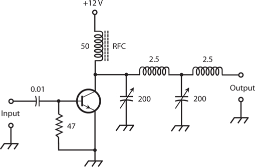
Figure 26-11 is a schematic diagram of a typical broadband PA using an NPN power transistor. This circuit can provide several watts of continuous RF power output over a range of frequencies from 1.5 MHz through 15 MHz. The transformers constitute a critical part of this circuit. They must work efficiently over a 10:1 range of frequencies. The 50-μH component labeled “RFC” is an RF choke, which passes DC and low-frequency AC while blocking high-frequency AC (that is, RF signals).

26-11 A broadband RF power amplifier, capable of producing a few watts output. Resistances are in ohms. Capacitances are in microfarads (μF). Inductances are in microhenrys (μH). The 50-μH component labeled “RFC” is an RF choke.
Tuned PAs
A tuned RF PA offers improved efficiency compared with broadband designs. The tuned circuits minimize the risk of spurious signals from earlier stages being amplified and transmitted over the air. Tuned PAs can work into a wide range of load impedances. In addition to a tuning control, or resonant circuit that adjusts the output of the amplifier to the operating frequency, the tuned amplifier incorporates a loading control that optimizes the signal transfer between the amplifier and the load (usually an antenna).
Tuned PAs have one significant limitation: The “tune-up” procedure (usually the adjustment of variable capacitors and/or variable inductors) takes time, and improper adjustment can result in damage to the transistor. If the tuning and/or loading controls aren’t properly set, the amplifier efficiency will drop to near zero, while the DC power input remains high. Solid-state devices overheat quickly under these conditions because the excess power “has nowhere to go” except to dissipate itself as heat in the amplifier’s components.
Figure 26-12 illustrates a tuned RF PA that can provide a few watts of useful power output at about 10 MHz. The transistor is the same type as the one used in the broadband amplifier of Fig. 26-11. The operator should adjust the tuning and loading controls (left-hand and right-hand variable capacitors, respectively) for maximum power output as indicated by an RF wattmeter.
26-12 A tuned RF power amplifier, capable of producing a few watts of output. Resistances are in ohms. Capacitances are in microfarads (μF) if less than 1, and in picofarads (pF) if more than 1. Inductances are in microhenrys (μH).
How Oscillators Work
An oscillator is a specialized amplifier with positive feedback. Radio-frequency oscillators generate signals in a wireless broadcast or communications system. Audio-frequency oscillators find applications in hi-fi systems, music synthesizers, electronic sirens, security alarms, and electronic toys.
Positive Feedback
Feedback normally occurs either in phase with the input signal, or in phase opposition relative to the input signal. If we want to make an amplifier circuit oscillate, we must introduce some of its output signal back to the input in phase (that’s called positive feedback). If we introduce some of the output signal back to the input in phase opposition, we have negative feedback that reduces the overall gain of the amplifier. Negative feedback is not always bad; engineers deliberately use it in some amplifiers to prevent unwanted oscillation.
The AC output signal wave from a common-emitter or common-source amplifier occurs in phase opposition with respect to the input signal wave. If you couple the collector to the base through a capacitor, you won’t get oscillation. You must invert the phase in the feedback process if you want oscillation to occur. In addition, the amplifier must exhibit a certain minimum amount of gain, and the coupling from the output to the input must be substantial. The positive feedback path must be easy for a signal to follow. Most oscillators comprise common-emitter or common-source amplifier circuits with positive feedback.
The AC output signal wave from a common-base or common-gate amplifier is in phase with the input signal wave. You might, therefore, suppose that such circuits would make ideal candidates for oscillators. However, the common-base and common-gate circuits produce less gain than their common-emitter and common-source counterparts, so it’s more difficult to make them oscillate. Common-collector and common-drain circuits are even worse in this respect because they have negative gain!
Feedback at a Single Frequency
We can control the frequency of an oscillator using tuned, or resonant, circuits, usually consisting of inductance-capacitance (LC) or resistance-capacitance (RC) combinations. The LC scheme is common in radio transmitters and receivers; the RC method is more often used in audio work. The tuned circuit makes the feedback path easy for a signal to follow at one frequency, but difficult to follow at all other frequencies. As a result, oscillation takes place at a stable frequency, determined by the inductance and capacitance, or by the resistance and capacitance.
Common Oscillator Circuits
Many circuit arrangements can reliably produce oscillation. The following several circuits all fall into a category known as variable-frequency oscillators (VFOs) because we can adjust their signal frequencies continuously over a wide range. Oscillators usually produce less than 1 W of RF power output. If we need more power, we’ll need to follow the oscillator with one or more stages of amplification.
The Armstrong Circuit
We can force a common-emitter or common-source class-A amplifier to oscillate by coupling the output back to the input through a transformer that reverses (inverts) the phase of the fed-back signal. The schematic diagram of Fig. 26-13 shows a common-source amplifier whose drain circuit is coupled to the gate circuit by means of a transformer. We control the frequency by adjusting a capacitor connected in series with the transformer secondary winding. The inductance of the transformer secondary, along with the capacitance, forms a resonant circuit that passes energy easily at one frequency, while attenuating (suppressing) the energy at other frequencies. Engineers call this type of circuit an Armstrong oscillator. We can substitute a bipolar transistor for the JFET, as long as we bias the device for class-A amplification.

26-13 An Armstrong oscillator using an N-channel JFET. This circuit constitutes a common-source amplifier with positive feedback through a tuned circuit.
The Hartley Circuit
Figure 26-14 illustrates another method of obtaining controlled RF feedback. In this example, we use a PNP bipolar transistor. The circuit has a single coil with a tap on the winding. A variable capacitor in parallel with the coil determines the oscillating frequency, and allows for frequency adjustment. This circuit is called a Hartley oscillator.

26-14 A Hartley oscillator using a PNP bipolar transistor. We can recognize the Hartley circuit by the tapped inductor in the tuned LC circuit.
In the Hartley circuit, as well as in most other RF oscillator circuits, we must always use the minimum amount of feedback necessary to obtain reliable, continuous oscillation. The location of the coil tap determines the amount of feedback. The circuit shown in Fig. 26-14 takes only about 25% of its amplifier power to produce the feedback. We can, therefore, use the other 75% of the power as useful signal output.
The Colpitts Circuit
We can tap the capacitance, instead of the inductance, in the tuned circuit of an RF oscillator. This arrangement gives us a Colpitts oscillator. Figure 26-15 is a schematic diagram of a P-channel JFET wired up to function as a Colpitts oscillator. We control the amount of feedback by “tweaking” the ratio of the two capacitances connected in parallel with the variable inductor, which provides for the frequency adjustment. The two capacitors across the variable inductor are fixed, not variable. This feature offers convenience and saves money because we’ll likely have trouble finding a dual variable capacitor that maintains the correct ratio of capacitances throughout its tuning range (as we would need if the inductor in the tuned circuit weren’t variable).

26-15 A Colpitts oscillator using a P-channel JFET. The Colpitts circuit can be recognized by the split capacitance in the tuned LC circuit.
Unfortunately, finding a variable inductor for use in a Colpitts oscillator can prove almost as difficult as obtaining a suitable dual variable capacitor. We can use a permeability-tuned coil, but ferromagnetic cores impair the frequency stability of an RF oscillator. We can use a roller inductor with an air core, but these components are bulky and expensive. We can use a fixed inductor with several switch-selectable taps, but this approach doesn’t allow for continuous frequency adjustment. Despite these shortcomings, the Colpitts circuit offers exceptional stability and reliability when properly designed.
The Clapp Circuit
A variation of the Colpitts oscillator employs series resonance, instead of parallel resonance, in the tuned circuit. Otherwise, the circuit resembles the parallel-tuned Colpitts oscillator. Figure 26-16 shows a series-tuned Colpitts oscillator circuit with an NPN bipolar transistor. Some engineers call it a Clapp oscillator.

26-16 A series-tuned Colpitts oscillator, also known as a Clapp oscillator. This circuit uses an NPN bipolar transistor.
A Clapp oscillator is a reliable circuit in general. We can easily get it to oscillate and keep it going. Its frequency won’t change much if we build it with high-quality components. The Clapp design allows us to employ a variable capacitor for frequency control, while accomplishing feedback through a capacitive voltage divider.
Getting the Output
Have you noticed something strange about the Hartley, Colpitts, and Clapp oscillators diagrammed in Figs. 26-14 through 26-16? If not, look again, and compare these circuits with class-A common-emitter and common-source amplifiers. In these oscillators, we take the output from the emitter or source, not from the collector or drain as we would normally do with an amplifier. Why, you ask, would we want to take this approach in oscillator design?
Theoretically, we can get the output of an oscillator from the collector or drain to get maximum gain. But in an oscillator, stability and reliability are more important than gain. We can get all the gain we want in amplifiers following an oscillator. We obtain better stability in an oscillator when we take the output signal from the emitter or source, as compared with taking it from the collector or drain. In that arrangement, variations in the load impedance have less effect on the frequency of oscillation, and a sudden decrease in load impedance is less likely to cause the oscillator to fail outright.
To prevent the output signal from shorting to ground, we can connect an RF choke (RFC) in series with the emitter or source in the Colpitts and Clapp oscillator circuits. The choke, which comprises a high-value inductor, allows DC to pass while blocking high-frequency AC (exactly the opposite behavior from that of a blocking capacitor). Typical values for RF chokes range from about 100 μH at high frequencies such as 15 MHz, to 10 mH at low frequencies, such as 150 kHz.
The Voltage-Controlled Oscillator
We can adjust the frequency of a VFO to some extent by connecting a varactor diode in the tuned LC circuit. Recall that a varactor, also called a varicap, is a semiconductor diode that functions as a variable capacitor when reverse-biased. As the reverse-bias voltage increases, the junction capacitance decreases, provided that we don’t apply so much voltage that avalanche breakdown occurs.
The Hartley and Clapp oscillator circuits lend themselves to varactor-diode frequency control. We can connect the varactor in series or in parallel with the main tuning capacitor. We must isolate the varactor for DC with blocking capacitors. If you look back to Chap. 20 for a moment and check Fig. 20-9, you’ll see an effective method of connecting a varactor in a tuned LC circuit. We call the resulting limited-range VFO a voltage-controlled oscillator (VCO).
Varactors cost less, weigh less, and take up less physical space than variable capacitors or inductors. These factors constitute the chief advantages of a VCO over an old-fashioned VFO that employs only a variable capacitor and a fixed inductor, or only a variable inductor and a fixed capacitor.
Diode-Based Oscillators
At ultra-high frequencies (UHF) and microwave radio frequencies, certain types of diodes can function as oscillators. In Chap. 20, you learned about these components, which include the Gunn diode, the IMPATT diode, and the tunnel diode.
Crystal-Controlled Oscillators
In an RF oscillator, we can use a quartz crystal in place of a tuned LC circuit, as long as we don’t have to change the frequency often. Crystal-controlled oscillators offer frequency stability superior to that of LC tuned VFOs.
Several schemes exist for the connection of quartz crystals into bipolar or FET circuits for the purpose of obtaining oscillation. One common circuit is the Pierce oscillator. We can obtain a Pierce oscillator by connecting a JFET and a quartz crystal, as shown in Fig. 26-17. This circuit takes advantage of an N-channel JFET, but we could just as well use an N-channel MOSFET, a P-channel JFET, or a P-channel MOSFET. The crystal frequency can be varied by about plus-or-minus a tenth of one percent (±0.1%, or one part in 1000) by means of an inductor or capacitor in parallel with the crystal. However, the oscillation frequency is determined mainly by the thickness of the quartz wafer, and by the angle at which it was cut from the original mineral sample.
26-17 A Pierce oscillator circuit using an N-channel JFET.
Crystals change in frequency as the temperature changes. But they’re far more stable than LC circuits, most of the time. If an engineer needs a crystal oscillator with exceptional frequency stability, the crystal can be enclosed in a temperature-controlled chamber called a crystal oven. In this environment, the crystal maintains its rated frequency so well that it can function as a frequency standard against which other frequency-dependent circuits, including oscillators, are calibrated.
The Phase-Locked Loop
One type of oscillator that combines the flexibility of a VFO with the stability of a crystal oscillator is the phase-locked loop (PLL). The PLL makes use of a circuit called a frequency synthesizer. The output of a VCO passes through a programmable multiplier/divider, a digital circuit that divides and/or multiplies the VCO frequency by integral (whole-number) values that we can freely choose. As a result, the output frequency can equal any rational-number multiple of the crystal frequency. We can, therefore, adjust a well-designed PLL circuit in small digital increments over a wide range of frequencies. Figure 26-18 is a block diagram of a PLL.

26-18 Block diagram of a phase-locked loop (PLL).
The output frequency of the multiplier/divider remains “locked,” by means of a phase comparator, to the signal from a crystal-controlled reference oscillator. As long as the output from the multiplier/divider stays exactly on the reference oscillator frequency, the two signals remain exactly in phase, and the output of the phase comparator equals zero (that is, 0 V DC). If the VCO frequency begins to gradually increase or decrease (a phenomenon known as oscillator drift), the output frequency of the multiplier/divider also drifts, although at a different rate. Even a frequency change of less than 1 Hz causes the phase comparator to produce a DC error voltage. This error voltage is either positive or negative, depending on whether the VCO has drifted higher or lower in frequency. We apply the error voltage to a varactor, causing the VCO frequency to change in a direction opposite to that of the drift, creating a DC feedback circuit that maintains the VCO frequency at a precise value. Engineers call it a loop circuit that locks the VCO onto a particular frequency by means of phase sensing—hence the expression phase-locked.
The key to the stability of the PLL lies in the fact that the reference oscillator employs crystal control. When you hear that a radio receiver, transmitter, or transceiver is synthesized, you can have reasonable confidence that a PLL determines its operating frequency. The stability of a synthesizer can be enhanced by using an amplified signal from the shortwave time-and-frequency broadcast station WWV at 2.5, 5, 10, or 15 MHz, directly as the reference oscillator. These signals remain frequency-exact to a minuscule fraction of 1 Hz because they’re controlled by atomic clocks. Most people don’t need precision of this caliber, so you won’t see consumer devices like ham radios and shortwave receivers with primary-standard PLL frequency synthesis. But some corporations and government agencies use the primary-standard method to ensure that their systems stay “on frequency.”
Oscillator Stability
In an oscillator, the term stability can have either of two distinct meanings: constancy of frequency (or minimal frequency drift), and reliability of performance.
Frequency Stability
In the design and construction of a VFO of any kind, the components—especially the capacitors and inductors—must, to the greatest extent possible, maintain constant values under all anticipated conditions.
Some types of capacitors hold their values better than others as the temperature rises or falls. Polystyrene capacitors behave very well in this respect. Silver-mica capacitors can work when polystyrene units aren’t readily available. Air-core coils exhibit the best temperature stability of all inductor configurations. They should be wound, when possible, from stiff wire with strips of plastic to keep the windings in place. Some air-core coils are wound on hollow cylindrical cores, made of ceramic or phenolic material. Ferromagnetic solenoidal or toroidal cores aren’t very good for use in VFO coils because these materials change permeability as the temperature varies. This variation alters the inductance, in turn affecting the oscillator frequency.
The best oscillators, in terms of frequency stability, are crystal-controlled. This category includes circuits that oscillate at the fundamental frequency of the quartz crystal, circuits that oscillate at one of the crystal harmonic frequencies, or PLL circuits that oscillate at frequencies derived from the crystal frequency by means of programmable multiplier/dividers.
Reliability
An oscillator should always start working as soon as we apply DC power. It should keep oscillating under all normal conditions. The failure of a single oscillator can cause an entire receiver, transmitter, or transceiver to stop working.
When an engineer builds an oscillator and puts it to use in a radio receiver, transmitter, or audio device, debugging is always necessary. Debugging comprises a trial-and-error process—often quite tedious—of getting the flaws or “bugs” out of the circuit so that it will work well enough to to be mass-produced. Rarely can an engineer build something “straight from the drawing board” and have it work perfectly on the first test! In fact, if you build two oscillators from the same diagram, with the same component types and values, you shouldn’t be surprised if one circuit works okay and the other one doesn’t work at all. Problems of this sort usually happen because of differences in the quality of components that don’t show up until you conduct “real-world” circuit tests.
Oscillators are designed to work into relatively high load impedances. If we connect an oscillator to a load that has a low impedance, that load will “try” to draw a lot of power from the oscillator. Under such conditions, even a well-designed oscillator might stop working or not start up, when we first switch it on. Oscillators aren’t meant to produce powerful signals; we can use amplifiers for that purpose! You need never worry that an oscillator’s load impedance might get too high. In general, as we increase the load impedance for an oscillator, its overall performance improves.
Audio Oscillators
Audio oscillators appear in myriad electronic devices including doorbells, ambulance sirens, electronic games, telephone sets, and toys that play musical tunes. All AF oscillators are, in effect, AF amplifiers with positive feedback.
Audio Waveforms
At AF, oscillators can use RC or LC combinations to determine the frequency, but RC circuits are generally preferred. If we want to build an audio oscillator using LC circuits, we’ll need large inductances requiring the use of ferromagnetic cores.
At RF, oscillators are usually designed to produce a sine-wave output. A pure sine wave represents energy at one and only one frequency. Audio oscillators, in contrast, don’t always concentrate all their energy at a single frequency. (A pure AF sine wave, especially if continuous and frequency-constant, can give you a headache!) The various musical instruments in a band or orchestra all sound different from each other, even when they all play a note at the same frequency. This difference in sound timbre (the “character” of the sound) arises from the fact that each instrument generates its own unique AF waveform. As you know, a clarinet sounds different than a trumpet, which in turn sounds different from a cello or piano, even if they all play the same note such as middle C.
Imagine that you use a time-domain laboratory display to scrutinize the waveforms of musical instruments. You can build an arrangement for this purpose with a high-fidelity microphone, a sensitive, low-distortion audio amplifier, and an oscilloscope. You’ll see that each instrument has its own “signature.” Therefore, each instrument’s unique sound qualities can be reproduced using AF oscillators whose waveform outputs match those of the instrument. Electronic music synthesizers use audio oscillators to generate the notes that you hear.
The Twin-T Oscillator
Figure 26-19 shows a popular AF circuit called a Twin-T oscillator that can serve well for general-purpose use. The frequency depends on the values of the resistors R and capacitors C. The output note constitutes a near-perfect sine wave, although not quite perfect. (The small amount of distortion helps to alleviate the “ear-brain irritation” typically produced by an absolutely pure AF sinusoid.) The circuit shown in this example uses two PNP bipolar transistors biased for class-A amplification.

26-19 A twin-T audio oscillator using two PNP bipolar transistors. The frequency is determined by the values of the resistors R and the capacitors C.
The Multivibrator
Another popular AF oscillator circuit makes use of two identical common-emitter or common-source amplifier circuits, hooked up so that the signal goes around and around between them. Lay people sometimes call this arrangement a “multivibrator,” although the technical term multivibrator more appropriately applies to various digital signal-generating circuits.
In the example of Fig. 26-20, two N-channel JFETs are connected to form a “multivibrator” for use at AF. Each of the two transistors amplifies the signal in class-A mode and inverts the phase. Every time the signal goes from any particular point all the way around the circuit, it arrives back at that point inverted twice so it’s in phase with its “former self,” producing positive feedback.

26-20 A “multivibrator” audio oscillator using two N-channel JFETs. The frequency is determined by the values of the inductor L and the capacitor C.
We can set the frequency of the oscillator of Fig. 26-20 by means of an LC circuit. The coil can have a ferromagnetic core because stability is not of great concern and because we need such a core to obtain enough inductance to produce resonance at AF. Toroidal or pot cores work well in this application. The value of L can range from about 10 mH to as much as 1 H. We choose the capacitance according to the formula for resonant circuits (which you learned earlier in this course), to obtain an AF output note at the frequency desired.
Integrated-Circuit Oscillators
In recent years, solid-state technology has advanced to the point that entire electronic systems can be etched onto silicon chips. Such devices have become known as integrated circuits (ICs). The operational amplifier, also called an op amp, is a type of IC that performs exceptionally well as an AF oscillator because it has high gain, and it can easily be connected to produce positive feedback. You learned about op amps in Chap. 23.
Quiz
Refer to the text in this chapter if necessary. A good score is at least 18 correct. Answers are in the back of the book.
1. Which of the following oscillator types should we expect to have the best frequency stability?
(a) Colpitts
(b) Clapp
(c) Hartley
(d) Pierce
2. If we increase the RMS voltage of a signal by a factor of 10,000 across a pure, constant resistance, we observe a signal gain of
(a) 100 dB.
(b) 80 dB.
(c) 40 dB.
(d) 20 dB.
3. Suppose that we supply 1.00 W of RMS input to an amplifier that provides a power gain of 33.0 dB. What’s the output, assuming that no reactance exists in the system?
(a) 2.00 kW RMS
(b) 330 W RMS
(c) 200 W RMS
(d) 50.0 W RMS
4. Imagine that we apply a signal of 30 V RMS to the primary winding of a perfectly efficient impedance-matching transformer (it dissipates no power as heat in its core or windings), obtaining 10 V RMS across the secondary. Also suppose that no reactance exists in the circuits connected to the primary and secondary. This transformer technically introduces
(a) a voltage loss of approximately 9.5 dB, which we can also call a voltage gain of approximately −9.5 dB.
(b) a voltage gain of approximately 4.8 dB, which we can also call a voltage loss of approximately −4.8 dB.
(c) a current loss of approximately 9.5 dB, which we can also call a current gain of approximately −9.5 dB.
(d) a current gain of approximately 4.8 dB, which we can also call a current loss of approximately −4.8 dB.
5. Which of the following components would we most likely choose if we want to allow DC to pass from one circuit point to another, but we want to keep high-frequency AC signals from following the same path?
(a) A varactor
(b) A blocking capacitor
(d) A Gunn diode
6. Figure 26-21 is a diagram of

26-21 Illustration for Quiz Questions 6 through 8.
(a) a Pierce oscillator.
(b) a class-B push-pull amplifier.
(c) an Armstrong oscillator.
(d) a broadband power amplifier.
7. What, if any, significant technical errors exist in the circuit in Fig. 26-21?
(a) No significant technical errors exist.
(b) The power supply polarity is wrong.
(c) We must use an enhancement-mode MOSFET, not a depletion-mode MOSFET.
(d) The transformer must have an air core, not a powdered-iron core.
8. What precaution must we observe if we expect the circuit of Fig. 26-21 to perform correctly?
(a) We must connect the transformer windings to ensure that the drain-to-gate feedback occurs in the proper phase.
(b) We must set the variable capacitor to obtain the maximum possible amplification factor.
(c) We must not allow the output load impedance to exceed the value of the resistor between the transformer primary and the source of DC voltage.
(d) All of the above
9. In which of the following bipolar-transistor amplifier types does collector current flow for less than half of the signal cycle?
(a) Class-C
(b) Class-B
(c) Class-AB2
(d) Class-AB1
10. When designing and testing a tuned class-B push-pull RF power amplifier, we must
(a) bias the transistors to ensure that collector or drain current flows in both devices during the entire AC input signal cycle.
(b) select the capacitors so as to allow the system to work over a wide range of frequencies without adjustment.
(c) set the output tuned circuit to resonate at an even harmonic of the input frequency.
(d) select two bipolar or field-effect transistors whose characteristics are as nearly identical as possible.
11. In a Hartley oscillator, the output-signal frequency depends on the
(a) gain of the transistor.
(b) tuned-circuit inductance and capacitance.
(c) dimensions of a quartz crystal.
(d) feedback path in a phase-locked loop (PLL).
12. Which FET amplifier type introduces little or no distortion into the AC signal wave, with drain current during the entire signal cycle?
(a) Class A
(b) Class AB1 or AB2
(c) Class B
(d) Class C
13. We can make a class-B amplifier linear for the AC signal waveform by
(a) minimizing the output impedance.
(b) biasing the transistor considerably past cutoff or pinchoff.
(c) connecting two transistors in a push-pull arrangement.
(d) no known means.
14. If we connect a load with very low, purely resistive impedance to the output of an oscillator, we
(a) maximize the output power.
(b) enhance the linearity, while allowing for harmonics.
(c) might have trouble adjusting the frequency.
(d) might have trouble getting the oscillator to start or keep going.
15. Suppose that a certain FET-based RF PA operates with an efficiency of 60%. We measure the DC drain input power as 90 W. We can have confidence that the RF signal output power is
(a) 54 W
(b) 90 W
(c) 150 W
(d) impossible to determine without more information.
16. Figure 26-22 illustrates a generic tuned, class-B RF PA. According to the knowledge of bipolar-transistor circuits that we’ve gained so far in this course, we can surmise that the capacitor labeled V

26-22 Illustration for Quiz Questions 16 through 20.
(a) provides proper bias for the transistor.
(b) allows the AC input signal to enter but provides DC isolation.
(c) determines the resonant frequency of the input circuit.
(d) keeps the signal from shorting through the power supply.
17. According to the knowledge of bipolar-transistor circuits that we’ve gained so far in this course, we can surmise that the resistor labeled W in Fig. 26-22
(a) provides proper bias for the transistor.
(b) allows the AC input signal to enter but provides DC isolation.
(c) determines the resonant frequency of the input circuit.
(d) keeps the signal from shorting through the power supply.
18. According to the knowledge of bipolar-transistor circuits that we’ve gained so far in this course, we can surmise that the RF choke labeled X in Fig. 26-22
(a) prevents excessive current from flowing in the collector.
(b) allows the AC output signal to leave but provides DC isolation.
(c) determines the resonant frequency of the output circuit.
(d) keeps the signal from shorting through the power supply.
19. According to the knowledge of bipolar-transistor circuits that we’ve gained so far in this course, we can surmise that the inductors labeled Y in Fig. 26-22
(a) help to optimize the signal transfer to the output.
(b) ensure that the output signal remains in phase with the input signal.
(c) provide enough feedback to keep the circuit from oscillating.
(d) keep the transistor from operating in a state of overdrive.
20. According to the knowledge of bipolar-transistor circuits that we’ve gained so far in this course, we can surmise that the capacitors labeled Z in Fig. 26-22
(a) help to optimize the signal transfer to the output.
(b) ensure that the output signal remains in phase with the input signal.
(c) provide enough feedback to keep the circuit from oscillating.
(d) keep the transistor from operating in a state of overdrive.