
22
CHAPTER
Field-Effect Transistors
THE BIPOLAR DEVICE ISN’T THE ONLY FORM OF TRANSISTOR THAT CAN SWITCH, AMPLIFY, OR OSCILLATE. A field-effect transistor (FET) can also do these things. Two main types of FET exist: the junction FET (JFET) and the metal-oxide-semiconductor FET (MOSFET).
Principle of the JFET
In a JFET, an electric field within the device affects the amount of current that can flow through it. Charge carriers (electrons or holes) move from the source (S) electrode to the drain (D) electrode to produce a drain current ID that normally equals the source current, IS. The rate of flow of charge carriers—that is, the current—depends on the voltage at a control electrode called the gate (G). Fluctuations in gate voltage EG cause changes in the current through the channel, the path that the charge carriers follow between the source and the drain. The current through the channel normally equals ID. Under the right conditions, small fluctuations in EG can cause large variations in ID. This fluctuating drain current can, in turn, produce significant fluctuations in the voltage across an output resistance.
N-Channel versus P-Channel
Figure 22-1 is a simplified drawing of an N-channel JFET (at A) and its schematic symbol (at B). The N type material forms the channel. The majority carriers in the channel are electrons, while the minority carriers are holes. We normally place the drain at a positive DC voltage with respect to the source, using an external power supply or battery.

22-1 At A, a simplified structural drawing of an N-channel JFET. We identify the electrodes as S = source, G = gate, and D = drain. At B, the schematic symbol.
In an N-channel device, the gate consists of P type material. Another section of P type material, called the substrate, forms a boundary on the side of the channel opposite the gate. The voltage on the gate produces an electric field that interferes with the flow of charge carriers through the channel. As EG becomes more negative, the electric field chokes an increasing amount of the current though the channel, so ID decreases.
A P-channel JFET (Figs. 22-2A and B) has a channel of P type semiconductor material. The majority charge carriers in the channel are holes, while the minority carriers are electrons. Using an external power supply or battery, we place the drain at a negative DC voltage with respect to the source. The more positive EG gets, the more the electric field chokes off the current through the channel, and the smaller ID becomes.

22-2 At A, a simplified structural drawing of a P-channel JFET. At B, the schematic symbol.
You can recognize the N-channel JFET in schematic diagrams by the presence of a small arrow pointing inward at the gate. You can recognize the P-channel JFET by the arrow pointing outward at the gate. Alternatively, you can tell the N-channel device from the P-channel device (in case the symbols lack arrows) by looking at the power-supply polarity. A positive drain indicates an N-channel JFET, and a negative drain indicates a P-channel JFET.
In electronic circuits, N-channel and P-channel devices can do the same kinds of things. The main difference lies in the power-supply or battery polarity. We can almost always replace an N-channel JFET with a P-channel JFET, reverse the polarity, and expect the circuit to work the same—assuming that the new device has the right specifications. Just as we’ll find different kinds of bipolar transistors, so will we encounter various types of JFETs, each suited to a particular application. Some JFETs work well as weak-signal amplifiers and oscillators; others find their niche in power amplification; some work ideally as high-speed switches.
Field-effect transistors have certain advantages over bipolar transistors. Perhaps the most important asset arises from the fact that JFETs, in general, create less internal noise than bipolar transistors do. This property makes JFETs excellent for use as weak-signal amplifiers at very high or ultra-high radio frequencies; in general, they do better than bipolar transistors in this respect. Field-effect transistors exhibit high input impedance values—in some cases so high that they draw virtually no current, while nevertheless providing significant signal output.
Depletion and Pinchoff
The JFET works because the voltage at the gate generates an electric field that interferes, more or less, with the flow of charge carriers along the channel. Figure 22-3 shows a simplified rendition of the situation for an N-channel device.

22-3 At A, the depletion region (darkest area) is narrow, the channel (white area) is wide, and many charge carriers (heavy dashed line) flow. At B, the depletion region is wider, the channel is narrower, and fewer charge carriers flow. At C, the depletion region obstructs the channel, and no charge carriers flow.
As the drain voltage ED increases, so does the drain current ID, up to a certain level-off value. This property holds true as long as the gate voltage EG remains constant, and doesn’t get too large (negatively). However, as EG becomes increasingly negative (Fig. 22-3A), a depletion region (shown as a solid dark area) begins to form in the channel. Charge carriers can’t flow in the depletion region, so they must pass through a narrowed channel.
As EG becomes more negative still, the depletion region widens, as shown in Fig. 22-3B. The channel narrows further, and the current through it declines some more. Ultimately, if the gate voltage becomes negative enough, the depletion region completely obstructs the flow of charge carriers, and the channel current drops to zero under no-signal conditions (Fig. 22-3C). We call this condition pinchoff. It’s the equivalent of cutoff in a bipolar transistor.
JFET Biasing
Figure 22-4 illustrates two biasing methods for N-channel JFET circuits. In Fig. 22-4A, we ground the gate through resistor R2. The source resistor R1 limits the current through the JFET. The drain current ID flows through R3, producing a voltage across R3. That resistor also keeps the output signal from “shorting out” through the power supply or battery. The AC output signal passes through C2 to the next circuit or load.

22-4 Two methods of biasing an N-channel JFET. At A, fixed gate bias; at B, variable gate bias.
In Fig. 22-4B, we connect the gate through potentiometer R2 to a source of voltage that’s negative with respect to ground. Adjusting this potentiometer results in a variable negative gate voltage EG between R2 and R3. Resistor R1 limits the current through the JFET. The drain current ID flows through R4, producing a voltage across it. This resistor also keeps the output signal from “shorting out” through the power supply or battery. The AC output signal passes through C2 to the next circuit or load.
In both circuits of Fig. 22-4, we provide the drain with a positive DC voltage relative to ground. For P-channel JFET circuits, simply reverse the polarities in Fig. 22-4, and replace the N-channel symbols with P-channel symbols.
Typical power-supply voltages in JFET circuits are comparable to those for bipolar transistor circuits. The voltage between the source and drain, abbreviated ED, can range from about 3 V to 150 V DC; most often it’s 6 to 12 V DC. The biasing arrangement in Fig. 22-4A works well for weak-signal amplifiers, low-level amplifiers, and oscillators. The scheme at B works well in power amplifiers having substantial input signal amplitudes.
Amplification
Figure 22-5 shows a graph of ID as a function of EG for a hypothetical N-channel JFET. We assume that drain voltage ED remains constant. When EG is fairly large and negative, the JFET operates in a pinched-off state, so no current flows through the channel. As EG gets less negative, the channel opens up, and ID begins flowing. As EG gets still less negative, the channel grows wider and ID increases. As EG approaches the point where the source-gate (S-G) junction (which constitutes a P-N junction) experiences forward breakover, the channel conducts as well as it possibly can; it’s “wide open.”

22-5 Relative drain current (ID) as a function of gate voltage (EG) for a hypothetical N-channel JFET.
If EG becomes positive enough so that the S-G junction goes past the forward-breakover point and conducts, some of the current in the channel “leaks out” through the gate. We rarely, if ever, want to see this state of affairs. We want the gate voltage to control the width of the channel and thereby control the current through it, but never to “suck” current out of it. Any current that flows out through the gate represents current that can’t contribute to the output of the JFET.
Think of a JFET channel as a garden hose. When you want to reduce the flow of water at the output end of a hose, you can insert an adjustable valve somewhere along the length of the hose, or you can step down on the hose to pinch it narrower. You would not want to punch a hole in the hose to reduce the flow at the output because that action would let water go to waste.
The FET Amplifies Voltage
We can obtain the best amplification for weak signals when we set the no-signal gate voltage EG so as to maximize the slope (“rise over run”) of the drain-current versus gate-voltage (ID versus EG) curve. In Fig. 22-5, the range marked X shows the general region where this ideal condition exists. For power amplification, in which the JFET receives an input signal that’s fairly strong to begin with, we’ll often get the best results when we bias the JFET at or beyond pinchoff, in the range marked Y.
In either circuit shown in Fig. 22-4, ID passes through the drain resistor. Small fluctuations in EG cause large changes in ID, and these variations in turn produce wide swings in the DC voltage across R3 (in the circuit at A) or R4 (in the circuit at B). The AC part of this voltage goes through capacitor C2, and appears at the output as a signal of much greater AC voltage than that of the input signal at the gate. The JFET, therefore, acts as a voltage amplifier.
Drain Current versus Drain Voltage
Do you suspect that the drain current ID, passing through the channel of a JFET, increases in a linear manner with increasing drain voltage ED? This notion seems reasonable, but it’s not what usually happens. Instead, ID rises for a while as ED increases steadily, and then ID starts to level off as we increase ED still more. We can plot ID graphically as a function of ED for various values of EG under no-signal conditions. When we do that, we get a family of characteristic curves.
Figure 22-6 shows a family of characteristic curves for a hypothetical N-channel JFET. Engineers want to see graphs like this when choosing a JFET to serve in a specialized role, such as weak-signal amplification, oscillation, or power amplification. The graph of ID versus EG, one example of which appears in Fig. 22-5, is also an important specification that engineers consider. Characteristic curves portray DC behavior only; such curves are always derived under no-signal conditions.

22-6 A family of characteristic curves for a hypothetical N-channel JFET.
Transconductance
We learned in Chap. 22 that the beta of a bipolar transistor tells us how well the device can amplify a signal in a practical circuit. We can also call the bipolar beta the dynamic current amplification. In a JFET, engineers call its equivalent the dynamic mutual conductance, or transconductance.
Refer again to Fig. 22-5. Suppose that we set the gate voltage EG at a certain value, resulting in a drain current ID. If the gate voltage changes by a small amount dEG, then the drain current will change by an increment dID. The transconductance gFS equals the ratio of the change in the drain current to the change in the gate voltage, as follows:
gFS = dID/dEG
The transconductance at any particular bias point translates to the slope (“rise over run”) of a line tangent to the curve of Fig. 22-5 at that point.
As we can see from Fig. 22-5, the value of gFS varies as we move along the curve. When we bias the JFET beyond pinchoff in the region marked Y, the slope of the curve equals zero; it’s a horizontal line. In the range marked Y, we’ll observe no fluctuation in ID when EG changes by small amounts. When there’s a change in EG, we’ll see a change in ID only when the channel conducts during at least part of the cycle of any input signal that we apply.
The region of greatest transconductance corresponds to the portion of the curve marked X, where the slope is the steepest. This region represents conditions under which we can derive the most gain from the device. Because this part of the curve constitutes a straight line, we can expect to get excellent linearity from any amplifier that we care to build with the JFET, provided that we keep the input signal from getting so strong that it drives the device outside of range X during any part of the cycle.
If we bias the JFET beyond the range marked X, the slope of the curve decreases, and we can’t get as much amplification as we do in the range marked X. In addition, we can’t expect the JFET to remain linear because the curve does not constitute a straight line in the “improper bias” range. If we keep on biasing the gate to greater and greater positive voltages, we get to the broken portion of the curve, arriving at the zone where the S-G junction goes past forward breakover and draws current out of the channel.
The MOSFET
The acronym MOSFET (pronounced “moss-fet”) stands for metal-oxide-semiconductor field-effect transistor. As with JFETs, two main types of MOSFET exist: The N-channel device and the P-channel device. Figure 22-7 shows a simplified cross-sectional drawing of an N-channel MOSFET along with the schematic symbol. The P-channel device and its symbol appear in Fig. 22-8.

22-7 At A, the functional structure of an N-channel MOSFET. At B, the schematic symbol. Electrodes are S = source, G = gate, and D = drain.

22-8 At A, the functional structure of a P-channel MOSFET. At B, the schematic symbol.
Extremely High Input Impedance
When engineers originally developed the MOSFET, they called it an insulated-gate field-effect transistor or IGFET. That’s still a pretty good term. The gate electrode is electrically insulated from the channel by a thin layer of dielectric material. As a result, the input impedance normally exceeds that of a JFET. In fact, the gate-to-source (G-S) resistance of a typical MOSFET compares favorably to the resistance of a capacitor of similar physical dimensions—it’s “almost infinity”!
Because of its extreme G-S resistance, a MOSFET draws essentially no current, and therefore, essentially no power, from the input signal source. This property makes the MOSFET ideal for use in low-level and weak-signal amplifier circuits. Because the G-S “capacitor” is physically tiny, its capacitance is tiny as well, so the device can function quite well up to ultra-high radio frequencies (above 300 MHz).
Despite their obvious advantages in the impedance and frequency-response departments, MOS devices suffer from a big shortcoming: They’re electrically fragile. When building or servicing circuits with MOS devices, technicians must use special equipment to ensure that their hands don’t carry “static electricity.” If a “static” discharge occurs through the dielectric of a MOS device, the dielectric will be permanently compromised, and the MOSFET must be discarded. Even a small electrostatic buildup can produce a discharge strong enough to destroy a MOSFET. Warm and humid climates offer little or no protection against this hazard.
Flexibility in Biasing
In electronic circuits, we can sometimes replace an N-channel JFET directly with an N-channel MOSFET, or a P-channel JFET with a P-channel MOSFET. However, in a few situations this simple substitution won’t work. The characteristic curves for MOSFETs differ qualitatively from the characteristic curves for JFETs with similar amplifying characteristics.
The main difference between MOSFET behavior and JFET behavior arises from the fact that in a MOSFET, the source and the gate do not come together as a P-N junction. Instead, the two electrodes are physically separated by a “gap” of dielectric, so forward breakover can’t occur. We can apply gate bias that’s far more positive than +0.6 V to an N-channel MOSFET, or a lot more negative than −0.6 V to a P-channel MOSFET, and we’ll never see current “leak” out through the gate as it would do in a JFET (unless, of course, we apply a voltage so great that arcing (sparking) takes place across the dielectric “gap”).
Figure 22-9 illustrates a family of characteristic curves for a hypothetical N-channel MOSFET under no-signal conditions. The horizontal axis portrays DC drain voltage, while the vertical axis portrays drain current. For any specific gate voltage, the drain current increases rapidly at first as we increase the drain voltage. However, as we continue to increase the drain voltage, the drain current rises at a slower rate, eventually leveling off. Once a particular ID-versus-ED curve has “flattened out,” we can’t increase the drain current any further by applying more DC drain voltage.

22-9 A family of characteristic curves for a hypothetical N-channel MOSFET.
Depletion Mode versus Enhancement Mode
In the FET devices we’ve discussed so far, the channel normally conducts; as the depletion region grows, choking off the channel, the charge carriers must pass through a narrower and narrower path. We call this state of affairs the depletion mode for a field-effect transistor. A MOSFET can also function in the depletion mode. The drawings and schematic symbols of Figs. 22-7 and 22-8 show depletion-mode MOSFETs. The characteristic curves in Fig. 22-9 illustrate the behavior of a typical depletion-mode N-channel MOSFET. (To get the graphs for a P-channel device, reverse all the polarities.)
Metal-oxide semiconductor technology also allows an entirely different means of operation. An enhancement-mode MOSFET normally has a pinched-off channel. We must apply a bias voltage EG to the gate so that a channel will form. If EG = 0 in an enhancement-mode MOSFET, then ID = 0 with no signal input. The enhancement-mode MOSFET, like its depletion-mode cousin, has an extremely low capacitance and high impedance between the gate and the channel.
In an N-channel enhancement-mode device, a positive voltage at the gate (with respect to the source) causes a conductive path to form in the channel. In the P-channel enhancement-mode device, we must apply a negative voltage at the gate in order to get the channel to conduct current. As the voltage increases, assuming the polarity is correct, the conductive channel grows wider, and the source-to-drain conductivity improves. This effect occurs, however, only up to a certain maximum current for a given constant DC drain voltage.
Figure 22-10 shows the schematic symbols for N-channel and P-channel enhancement-mode devices. Note that the vertical line is broken, rather than solid as it appears in the symbol for a depletion-mode MOSFET.

22-10 Schematic symbols for enhancement–mode MOSFETs. At A, the N-channel device; at B, the P-channel device.
Common-Source Configuration
In a common-source circuit, we place the source at signal ground and apply the input signal to the gate. Figure 22-11 shows the general configuration for an N-channel JFET. The device could be an N-channel, depletion-mode MOSFET and the circuit arrangement would look the same. For an N-channel, enhancement-mode device, we would need an extra resistor between the gate and the positive power supply terminal. For P-channel devices, the schematics would be the same except that the supply would provide a negative, rather than a positive, voltage.
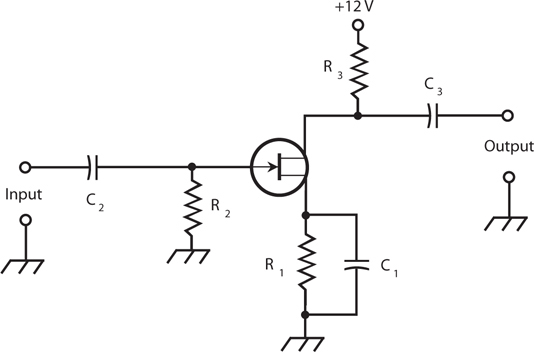
22-11 Common-source configuration. This diagram shows an N-channel JFET circuit.
Capacitor C1 and resistor R1 place the source at signal ground, while elevating the source above ground for DC. The AC signal enters through C2. Resistor R2 adjusts the input impedance and provides bias for the gate. The AC signal passes out of the circuit through C3. Resistor R3 keeps the output signal from being shorted out through the power supply, while allowing for a positive voltage at the drain. This circuit can serve as the basic configuration for low-level RF amplifiers and oscillators.
The common-source arrangement provides the greatest gain of the three FET circuit configurations. The output wave appears in phase opposition with respect to the input wave.
Common-Gate Configuration
In the common-gate circuit (Fig. 22-12), we place the gate at signal ground and apply the input signal to the source. This diagram shows an N-channel JFET. For other types of FETs, the same considerations, as described above for the common-source circuit, apply. Enhancement-mode devices require an extra resistor between the gate and the positive supply terminal (or the negative terminal if the MOSFET is P-channel).

22-12 Common-gate configuration. This diagram shows an N-channel JFET circuit.
The DC bias for the common-gate circuit is basically the same as that for the common-source arrangement, but the signal follows a different path. The AC input signal enters through C1. Resistor R1 keeps the input signal from shorting out to ground. Gate bias is provided by R1 and R2. Capacitor C2 places the gate at signal ground. (In some common-gate circuits, the gate goes directly to ground, and R2 and C2 are not used.) The output signal leaves the circuit through C3. Resistor R3 keeps the output signal from shorting out through the power supply, while still allowing the FET to receive the necessary DC voltage.
The common-gate arrangement produces less gain than its common-source counterpart, but it’s far less likely to break into unwanted oscillation, making it a good choice for RF power-amplifier circuits. The output wave follows along in phase with the input wave.
Common-Drain Configuration
Figure 22-13 shows a common-drain circuit. We place the drain at signal ground. It is sometimes called a source follower because the output waveform follows the signal at the source. The FET is biased in the same way as for the common-source and common-gate circuits. In Fig. 22-13, we see an N-channel JFET, but any other kind of FET could be used, reversing the polarity for P-channel devices. Enhancement-mode MOSFETs would need an extra resistor between the gate and the positive supply terminal (or the negative terminal if the MOSFET is P-channel).

22-13 Common-drain configuration, also known as a source follower. This diagram shows an N-channel JFET circuit.
The input signal passes through C2 to the gate. Resistors R1 and R2 provide gate bias. Resistor R3 limits the current. Capacitor C3 keeps the drain at signal ground. Fluctuating DC (the channel current) flows through R1 as a result of the input signal; this causes a fluctuating DC voltage to appear across R1. We take the output from the source, and its AC component passes through C1.
The output wave of the common-drain circuit is in phase with the input wave. This scheme constitutes the FET equivalent of the bipolar common-collector (emitter follower) arrangement. The output impedance is low, so this type of circuit works quite well for matching a high input impedance to a low output or load impedance over a wide range of frequencies.
Quiz
Refer to the text in this chapter if necessary. A good score is at least 18 correct. Answers are in the back of the book.
1. In a JFET, current through the channel varies because of the effects of
(a) a magnetic field.
(b) an electric field.
(c) leakage current.
(d) avalanche current.
2. In a P-channel JFET, assuming that the drain voltage remains constant, pinchoff occurs when we place the gate at a
(a) tiny negative voltage with respect to the source.
(b) significant negative voltage with respect to the source.
(c) tiny positive voltage with respect to the source.
(d) significant positive voltage with respect to the source.
3. When we bias a JFET at the point on its ID versus EG curve at which we can expect to derive the most amplification, the value of dID/dEG, representing the slope of the curve at that point, is
(a) zero (“running horizontally”) with no signal input, and the curve appears as a straight line near the point.
(b) positive (“ramping upward to the right”) with no signal input, and the curve appears as a straight line near the point.
(c) negative (“ramping downward to the right”) with no signal input, and the curve bends downward near the point.
(d) positive (“ramping upward to the right”) with no signal input, and the curve bends downward near the point.
4. Under no-signal conditions, a zero-biased enhancement-mode MOSFET operates in a state of
(a) pinchoff.
(b) avalanche breakdown.
(c) saturation.
(d) forward breakover.
5. Figure 22-14 is a simplified cutaway diagram of

22-14 Illustration for Quiz Questions 5 and 6.
(a) a P-channel JFET.
(b) an N-channel JFET.
(c) a P-channel MOSFET.
(d) an N-channel MOSFET.
6. In Fig. 22-14, the item marked X constitutes
(a) a thin wafer of N type material.
(b) a thin layer of dielectric material.
(c) a thin layer of highly conductive material.
(d) a P-N junction.
7. A bipolar transistor might work better than a JFET or MOSFET when we want an amplifier to
(a) have good weak-signal performance.
(b) have low input impedance.
(c) produce high transconductance.
(d) draw the most possible power from the input signal source.
8. A properly operating MOSFET presents a G-S resistance
(a) of practically zero.
(b) lower than that of a JFET.
(c) comparable to that of a similar-sized capacitor.
(d) lower than that of a bipolar transistor.
9. In a FET of any kind, we generally don’t want to see DC flow between the
(a) source and the drain.
(b) source and the channel.
(c) drain and the channel.
(d) gate and the channel.
10. In a MOSFET, the majority carriers are electrons
(a) if the device has an N-type channel.
(b) when forward breakover occurs.
(c) when avalanche breakdown occurs.
(d) under no circumstances.
11. Which of the following circuits produces an output signal wave that’s precisely in phase with the input signal wave?
(a) The common-gate circuit
(b) The common-drain circuit
(c) The source follower
(d) All of the above
12. A small electrostatic discharge, such as might appear on a technician’s hands, can easily destroy a MOSFET by
(a) fusing the source to the drain.
(b) eliminating the charge carriers in the channel.
(c) destroying the insulating properties of the dielectric.
(d) causing forward breakover at the gate-drain junction.
13. A significant difference between MOSFETs and JFETs is the fact that
(a) JFETs usually have lower input impedances.
(b) JFETs are less electrically rugged.
(c) JFETs are physically larger.
(d) JFETs require far higher operating voltages.
14. We can recognize a depletion-mode MOSFET (as opposed to an enhancement-mode MOSFET) in schematic diagrams by the presence of
(a) an arrow pointing inward.
(b) a broken vertical line inside the circle.
(c) an arrow pointing outward.
(d) a solid vertical line inside the circle.
15. In a source follower, from which two points do we obtain the output signal?
(a) The drain and ground
(b) The drain and gate
(c) The gate and source
(d) The source and ground
16. Figure 22-15 illustrates a source follower with two major errors. To correct one of the errors, we must

22-15 Illustration for Quiz Questions 16 and 17.
(a) transpose the input and output terminals.
(b) replace the JFET with a depletion-mode MOSFET.
(c) replace the JFET with an enhancement-mode MOSFET.
(d) replace the gate resistor with a capacitor.
17. To correct the second error in Fig. 22-15, we must
(a) connect the drain directly to the positive DC voltage source by replacing the drain resistor with a length of wire.
(b) replace the gate capacitor with a resistor.
(c) replace the source capacitor with a resistor.
(d) reverse the DC power-supply polarity.
18. Figure 22-16 illustrates a family of characteristic curves for a hypothetical N-channel, depletion-mode MOSFET. The curves V through Z portray the behavior of the device for various

22-16 Illustration for Quiz Questions 18 through 20.
(a) DC source voltages under no-signal conditions.
(b) AC input signal voltages.
(c) DC gate voltages under no-signal conditions.
(d) AC output signal voltages.
19. What can we say about the relative voltages for curves V through Z in Fig. 22-16? Remember, we’re dealing with an N-channel, depletion-mode MOSFET.
(a) They’re DC voltages that get progressively less positive (or more negative) as we proceed down from V to Z.
(b) They’re DC voltages that get progressively less negative (or more positive) as we proceed down from V to Z.
(c) They’re AC voltages whose peak-to-peak values increase as we proceed down from V to Z.
(d) They’re AC voltages whose peak-to-peak values decrease as we proceed down from V to Z.
20. Notice how all the curves in Fig. 22-16 tend to “level off” as we move toward the right in the coordinate grid. What does the “leveling-off” tell us about the general behavior of this particular N-channel, depletion-mode MOSFET?
(a) As we increase the positive DC drain voltage under no-signal conditions, the drain current increases slowly at first, then more and more rapidly.
(b) As we increase the positive DC drain voltage under no-signal conditions, the drain current increases rapidly at first, then more and more slowly.
(c) As we increase the peak-to-peak AC input signal voltage, the drain current increases slowly at first, then more and more rapidly.
(d) As we derive increasing peak-to-peak AC output signal voltage from the device, the drain current increases rapidly at first, then more and more slowly.