
Chapter 4
Sneak Circuits of Soft-Switching Converters
4.1 Introduction
Soft-switching is a technique that makes use of capacitor, inductor, and other components to realize resonance, for reducing the switching losses of switching components and EMI in the power electronic converter. As a result of adding resonant components such as capacitor or inductor into the soft-switching converter, it is certain that the soft-switching converter will have more current paths than the hard-switching converter. Consequently, the sneak circuit phenomena in the soft-switching converter will be more complex than those in the hard-switching converter.
According to the development of the soft-switching technique, the soft-switching converter can be divided into three types, including the quasi-resonant converter, the zero-switching pulse-width modulation (PWM) converter, and the zero-transition PWM converter. In this chapter, the sneak circuit phenomena of several typical soft-switching converters will be introduced.
4.2 Sneak Circuits of Full-Bridge ZVS PWM Converter
Among the DC/DC converters, the Full-bridge (FB) PWM converter is generally used in high-power applications, and the phase-shift technique is often used to control an FB converter, which can make the converter operate in zero voltage switching (ZVS). The basic soft-switching principle of the FB PWM converter is that ZVS of all switching devices can be achieved by the resonance between the leakage inductor of the transformer or the inductor in series with the transformer primary side and the parasitic capacitor of switches. The normal operating mode of the FB ZVS PWM converter will be introduced first.
4.2.1 Normal Operating Mode of FB ZVS PWM Converter
A schematic diagram of a conventional FB ZVS PWM converter is shown in Figure 4.1, where D1 to D4 is the anti-parallel diodes of switches Q1 to Q4, respectively, C1 to C4 are the parasitic capacitors or external paralleled capacitors of Q1 to Q4, respectively, and Lr represents the total resonant inductor of the leakage inductor of the transformer and the additional inductor in series with the transformer primary side. The fundamental operating principle of the FB ZVS PWM converter is that a pair of switches in each bridge leg conduct complementarily by 180 degrees and the conduction angle of the two bridge legs differ in a fixed phase, where the switching transition of leg Q1–Q3 is delayed, that is, phase shifted, with respect to the switching transition of leg Q2–Q4. Then leg Q1–Q3 becomes known as the lagging leg, and leg Q2–Q4 the leading leg. Typical waveforms of an FB ZVS PWM converter under normal operation are shown in Figure 4.2.

Figure 4.1 Schematic diagram of a FB ZVS PWM converter
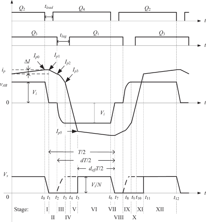
Figure 4.2 Typical waveforms of a FB ZVS PWM converter under normal operation
The output voltage of an FB ZVS PWM converter can be controlled by duty ratio d of the switches. However, the loss of duty ratio in the secondary side is a common phenomenon in the FB ZVS PWM converter; based on reference [1], the actual output voltage is expressed by
where deff is the effective duty ratio in the transformer secondary side. The relationship between the effective duty ratio deff and the duty ratio d in the transformer primary side is
where ![]() is the switching frequency, T is the switching cycle, RL is the load resistance, and N is the turns ratio of the transformer.
is the switching frequency, T is the switching cycle, RL is the load resistance, and N is the turns ratio of the transformer.
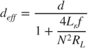
As shown in Figure 4.2, the normal operating process of an FB ZVS PWM converter can be divided into twelve stages in one switching period T, and the equivalent circuits of the first six stages are illustrated in Figure 4.3.
Figure 4.3 Equivalent circuits of the normal operating stages I to VI of a FB ZVS PWM converter: (a) stage I; (b) stage II; (c) stage III; (d) stage IV; (e) stage V; and (f) stage VI
The analysis of normal operating mode will be described before the following assumptions are made:
- All elements in the FB ZVS PWM converter are ideal.
- The paralleled capacitors of switches are defined by
 and
and  , but the capacitance between the transformer winding is ignored.
 - The filter inductance Lf satisfies
 .
.
Before stage I (or when ![]() ), Q2 and Q3 are conducting, the current of the primary side ip is positive, the output voltage of FB
), Q2 and Q3 are conducting, the current of the primary side ip is positive, the output voltage of FB ![]() , the rectifier diode DR2 is conducting, and the load is supplied by the input voltage source. As shown in Figure 4.2, the value of ip at
, the rectifier diode DR2 is conducting, and the load is supplied by the input voltage source. As shown in Figure 4.2, the value of ip at ![]() equates to
equates to
where ![]() is the average output current and ΔI is the primary current ripple during the conduction, which can be given by
is the average output current and ΔI is the primary current ripple during the conduction, which can be given by

It is known that ![]() , so Equation 4.4 can be simplified to
, so Equation 4.4 can be simplified to

In Equation 4.5, ΔI can be regarded as the current ripple of the output filter inductor converting to the primary side.
The analysis of the first six stages are described by the following.
Stage I (t0, t1)
Referring to Figure 4.3a, switch Q2 is turned off at t0, then the primary current ip charges the paralleled capacitor C2 of Q2 and discharges the paralleled capacitor C4 of Q4. vC2 will increase from zero and Q2 can achieve zero-voltage turn-off. ![]() in stage I; meanwhile, as the primary resonant inductor Lr and the filter inductor Lf are connected in series, the total inductance is very large, ip is approximately constant, and ip and vAB can be given by
in stage I; meanwhile, as the primary resonant inductor Lr and the filter inductor Lf are connected in series, the total inductance is very large, ip is approximately constant, and ip and vAB can be given by
Capacitor voltage vC4 (i.e., vAB) decreases from Vi linearly. Assuming that vC4 falls to zero at t1, then D4, the anti-parallel diode of Q4, will conduct and stage I will be finished. The duration of stage I is defined by
Stage II (t1, t2)
Referring to Figure 4.3b, Q4 can be turned on at ZVS after D4 conducts, because D4 clamps vQ4 to almost zero. Although Q4 has been turned on, the positive primary current ip is still running through D4, and there is no current passing through Q4. As ![]() in stage II, ip is equal to the filter inductor current converting to the primary side, which is
in stage II, ip is equal to the filter inductor current converting to the primary side, which is
Assuming that Q3 is turned off at t2, the primary current ip at ![]() can be approximated by
can be approximated by
The dead time between switches Q2 and Q4 of the leading leg, tlead, should be larger than ![]() , to achieve ZVS of Q4, then should satisfy
, to achieve ZVS of Q4, then should satisfy
Stage III (t2, t3)
Referring to Figure 4.3c, Q3 is turned off at t2, and the primary current ip transfers to C1 and C3, where C1 charges and C3 discharges. Due to C3 is the paralleled capacitor of Q3, vQ3 or vC3 will rise from zero slowly, then Q3 can be turned off at ZVS. Since ![]() in stage III, the secondary voltage of the transformer becomes negative, then the rectifier diode DR1 conducts too. Both the primary and secondary voltages of the transformer are zero because the secondary windings of the transformer are shorted by DR1 and DR2, then the voltage on the filter inductor vLr is equal to vAB. Lr resonates with C1 and C3 during this stage. ip and vC3 can be given by
in stage III, the secondary voltage of the transformer becomes negative, then the rectifier diode DR1 conducts too. Both the primary and secondary voltages of the transformer are zero because the secondary windings of the transformer are shorted by DR1 and DR2, then the voltage on the filter inductor vLr is equal to vAB. Lr resonates with C1 and C3 during this stage. ip and vC3 can be given by
where ![]() and
and ![]() .
.
Assuming that vC3 rises to Vi at t3, D1 begins to conduct, and stage III is ended, the duration of stage III is
where ![]() .
.
At ![]() , the value of the primary current ip is
, the value of the primary current ip is
Stage IV (t3, t4)
Referring to Figure 4.3d, Q1 can be turned on at ZVS because its voltage is clamped to almost zero after D1 conducts. Because ip is still positive, there is no current passing through Q1; ip flows through D1 and D3, and the stored energy in the resonant inductor Lr will feed back to the voltage source Vi. Since the voltages of the transformer primary and secondary sides are zero, ![]() in stage IV, and ip decreases linearly and is expressed by
in stage IV, and ip decreases linearly and is expressed by
Assuming that ip falls to zero at t4, and both D1 and D4 are off, then the duration of stage IV is defined by
As shown in Figure 4.2, the time between when Q3 is shut down and Q1 is turned on is defined as the dead time of the lagging leg, that is, tlag. Based on the above analysis, in order to achieve ZVS of lagging leg, tlag must satisfy ![]() , which is
, which is
Based on Equation 4.18, there are ![]() and
and ![]() .
.
Stage V (t4, t5)
Referring to Figure 4.3e, as ip is too small to afford the load current, both of the rectifier diodes keep conducting, and the transformer primary and secondary voltages are zero as well as stage IV. Because of ![]() , ip increases linearly reversed and flows through Q1 and Q4, which can be given by
, ip increases linearly reversed and flows through Q1 and Q4, which can be given by
Assuming that ip is equal to the load current reflected to the primary side at t5, we have
At this moment, DR2 is off, stage V is ended, and the entire load current will flow through DR1 only.
Stage VI (t5, t6)
Referring to Figure 4.3f, Q1 and Q4 keep conducting, the load current is provided by the input voltage source, and ip can be defined by
When Q4 is turned off at t6 and stage VI is ended, the FB ZVS PWM converter begins to operate in another half cycle, where the operation of the next six stages are similar to those of stages I to VI.
4.2.2 Zero Voltage Switching Conditions of FB ZVS PWM Converter
In order to achieve ZVS of all switches in the FB PWM converter, there should be enough energy to make the voltage of the parasitic capacitor or external additional capacitor resonate to zero before the switch is turned on, and charge the parasitic capacitor or external additional capacitor of the other switch in the same leg to the input voltage Vi.
During the switching transition between Q2 and Q4 on the leading leg, that is, stages I and II, the output filter inductor Lf is in series with the resonant inductor Lr, and the energy stored in Lf and Lr is large enough to achieve ZVS. However, as the secondary side of the transformer is shortened during the switching transition between switches Q1 and Q3 on the lagging leg, that is, stages III and IV, only the energy stored in Lr is used to achieve ZVS, which is relatively small. As a result, it is easy to obtain ZVS for switches Q2 and Q4 on the leading leg, but difficult for Q1 and Q3 on the lagging leg [2].
On the basis of the above analysis, the ZVS conditions of the FB ZVS PWM converter are expressed by

Defining the critical current Icrit as

then the sub-equation ![]() in Equation 4.22 changes to
in Equation 4.22 changes to
or the load current should satisfy with
4.2.3 Sneak Circuit Phenomena of FB ZVS PWM Converter
For the FB ZVS PWM converter, if the input voltage Vi or load resistance RL is changed, or the dead times between switches (tlead or tlag) are not set in a reasonable range, then ZVS may not be realized, and the current will not flow in the presetting paths, or some new current paths will show up, therefore the sneak circuit phenomena will appear.
Based on Equation 4.22, it is clear that the ZVS conditions of the FB ZVS PWM converter can be divided into ZVS time condition and ZVS current condition; no matter which condition is not satisfied, the sneak circuit phenomena will occur. The following sneak circuit analysis will be classified by taking the ZVS current condition into account. Similar to normal operation, only the operating process in the positive half cycle will be analyzed.
4.2.3.1 Sneak Circuit Analysis under the ZVS Current Condition
When the ZVS current condition of the FB ZVS PWM converter, that is, Equation 4.24 is satisfied, there are three kinds of sneak circuit phenomena.
Sneak Circuit Phenomenon I
According to Equations 4.10 and 4.14, when the operating condition of the converter is changed, for example, the load resistance RL is increased which causes Ip2 to decrease and tlag−min to increase, while tlead, tlag, and Icrit remain unchanged. When
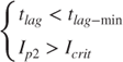
is satisfied, Q1 have to be turned on before stage III is completed (or vAB reaches to −Vi), then the zero-voltage turn-on cannot be realized. Furthermore, a new operating stage A will appear after stage III. The equivalent circuit of sneak stage A is shown in Figure 4.4.

Figure 4.4 Equivalent circuit of sneak stage A
As Q1 is turned on during the resonant process of C1, C3, and Lr, vC1 will discharge to zero and vC3 will charge to Vi immediately. When the sneak stage A is ended, the primary current ip flows through the freewheeling diodes D1 and D4, which is the same as normal stage IV. Then the converter will operate in normal stages IV, V, and VI after sneak stage A. The typical waveforms of sneak circuit phenomenon I are shown in Figure 4.5.

Figure 4.5 Typical waveforms of sneak circuit phenomenon I of a FB ZVS PWM converter
Sneak Circuit Phenomenon II
In the normal operating mode, Q1 should be turned on during stage IV to achieve ZVS. If ![]() is satisfied, namely Q1 does not turn on, even if stage IV is finished, then a new operating stage B will appear, whose equivalent circuit is shown in Figure 4.6a.
is satisfied, namely Q1 does not turn on, even if stage IV is finished, then a new operating stage B will appear, whose equivalent circuit is shown in Figure 4.6a.

Figure 4.6 Equivalent circuits of sneak stages B and C: (a) sneak stage B; and (b) sneak stage C
During sneak stage B, Lr will resonate with C1 and C3 again, and as Q1 is still off, ip will increase reversed from zero and vC3 will decrease. The expressions of ip and vC3 are
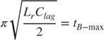
If Q1 is not turned on before vC3 decreases to zero, then sneak stage B is finished when ![]() , and the maximum duration of sneak stage B is defined by
, and the maximum duration of sneak stage B is defined by

If Q1 is turned on during stage B, that is, the lagging dead time satisfies ![]() , then Q1 will not realize ZVS because vC3 does not decrease to zero. Furthermore, a new stage C will show up, as shown in Figure 4.6b.
, then Q1 will not realize ZVS because vC3 does not decrease to zero. Furthermore, a new stage C will show up, as shown in Figure 4.6b.
As Q1 has been turned on, vC1 discharges to zero and vC3 rapidly charges to Vi , and ip remains almost constant because of the existence of resonant inductance Lr. When ![]() , the sneak stage C is ended, so the converter will operate in normal stages V and VI.
, the sneak stage C is ended, so the converter will operate in normal stages V and VI.
In summary, the condition of sneak circuit phenomenon II is given by Equation 4.30, and its corresponding typical waveforms are shown as Figure 4.7.


Figure 4.7 Typical waveforms of the sneak circuit phenomenon II of a FB ZVS PWM converter
Sneak Circuit Phenomenon III
If Q1 is still off when sneak stage B is over, that is, ![]() , then another new stage D will appear, as shown in Figure 4.8.
, then another new stage D will appear, as shown in Figure 4.8.

Figure 4.8 Equivalent circuit of the sneak stage D
During sneak stage D, because ![]() and
and ![]() , ip flows through D3 and Q4 and remains almost constant, and Q1 cannot realize zero voltage turn-on. When Q1 is turned on, the converter will operate in stages C, V, and VI until Q4 is turned off.
, ip flows through D3 and Q4 and remains almost constant, and Q1 cannot realize zero voltage turn-on. When Q1 is turned on, the converter will operate in stages C, V, and VI until Q4 is turned off.
Based on the above analysis, the condition of sneak circuit phenomenon III can be expressed as

and the typical waveforms of sneak circuit phenomenon III are shown in Figure 4.9.

Figure 4.9 Typical waveforms of the sneak circuit phenomenon III of a FB ZVS PWM converter
4.2.3.2 Sneak Circuit Analysis out of the ZVS Current Condition
When the ZVS current condition of an FB ZVS PWM converter is not satisfied, there are also three kinds of sneak circuit phenomena, which are numbered as IV to VI.
Sneak Circuit Phenomenon IV
If ![]() is satisfied by changing the converter parameters, such as increasing the load resistance RL, according to Equation 4.13, the maximum value of capacitor voltage vC3 during normal stage III will be
is satisfied by changing the converter parameters, such as increasing the load resistance RL, according to Equation 4.13, the maximum value of capacitor voltage vC3 during normal stage III will be
Therefore, it is impossible to realize ZVS of Q1. If Q1 is turned on before vC3 increases to VC3, this means that the duration of normal operating stage III satisfies ![]() , thus
, thus
and the operating process and typical waveforms are similar to those of sneak circuit phenomenon I, but the sneak circuit condition is different. So this situation is called the sneak circuit phenomenon IV, and its condition is expressed as
Sneak Circuit Phenomenon V
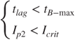
If the fixed lagging dead time tlag is longer than tB−max, that is, ![]() , Q1 will not be turned on after stage III, then Lr will keep resonant with C1 and C3, ip increases negatively from zero, and vC3 begins to decrease, which is the same as the sneak stage B.
, Q1 will not be turned on after stage III, then Lr will keep resonant with C1 and C3, ip increases negatively from zero, and vC3 begins to decrease, which is the same as the sneak stage B.
Based on Equation 4.29, if Q1 is turned on before stage B is ended, that is, ![]() , this means that Q1 is turned on before vC3 decreases to zero, and Q1 cannot be turned on with ZVS. After Q1 is turned on, the converter will operate at stages C, V, and VI until Q4 is turned off.
, this means that Q1 is turned on before vC3 decreases to zero, and Q1 cannot be turned on with ZVS. After Q1 is turned on, the converter will operate at stages C, V, and VI until Q4 is turned off.
Based on the above analysis, the typical waveforms of sneak circuit phenomenon V are shown in Figure 4.10, and the condition of sneak circuit phenomenon V can be expressed by


Figure 4.10 Typical waveforms of the sneak circuit phenomenon V of a FB ZVS PWM converter
Sneak Circuit Phenomenon VI
If the fixed lagging dead time satisfies ![]() when some operating conditions are changed, Q1 will be turned on after stage B is ended. Similar to sneak circuit phenomenon III, the converter will operate at stages D, C, V, and VI until Q4 is turned off, thus the typical waveforms of sneak circuit phenomenon VI appear as shown in Figure 4.11.
when some operating conditions are changed, Q1 will be turned on after stage B is ended. Similar to sneak circuit phenomenon III, the converter will operate at stages D, C, V, and VI until Q4 is turned off, thus the typical waveforms of sneak circuit phenomenon VI appear as shown in Figure 4.11.
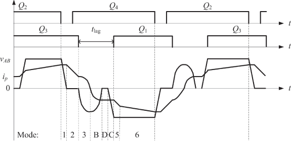
Figure 4.11 Typical waveforms of the sneak circuit phenomenon VI of a FB ZVS PWM converter
The condition of sneak circuit phenomenon VI can be expressed by

4.2.4 Operating Conditions of FB ZVS PWM Converter
As described above, all kinds of operating conditions of the FB ZVS PWM converter, including the normal mode and sneak circuit phenomena, are summarized in Table 4.1.
Table 4.1 Operating conditions of an FB ZVS PWM converter
| Phenomenon | Current condition | Time condition (tlag) | Time condition (tlead) |
| Normal | |||
| Sneak circuit phenomenon I | |||
| Sneak circuit phenomenon II | |||
| Sneak circuit phenomenon III | |||
| Sneak circuit phenomenon IV | |||
| Sneak circuit phenomenon V | |||
| Sneak circuit phenomenon VI |
Notes: ![]() ,
, ![]() ,
, ![]() , and
, and ![]() .
.
It is found that the reasonable range of the lagging dead time tlag is related to Ip2, which is the value of the primary current ip at ![]() . Substituting Equations 4.1, 4.2, and 4.5 into Equation 4.10, Ip2 is defined by
. Substituting Equations 4.1, 4.2, and 4.5 into Equation 4.10, Ip2 is defined by
Therefore, any variation of input voltage Vi, output voltage Vo (or duty ratio d), switching frequency f, or load resistance RL will change the value of Ip2, which may result in sneak circuit phenomenon.
4.2.5 Experimental Verification of FB ZVS PWM Converter
A FB ZVS PWM prototype based on Figure 4.1 has been implemented to demonstrate the sneak circuit phenomena and the corresponding conditions. In the prototype, IRFZ44N and SR506 are selected as switch and diode respectively, the control IC is UC3879 and the driving IC is IR2110, and the other parameters are ![]() ,
, ![]() ,
, ![]() ,
, ![]() ,
, ![]() ,
, ![]() ,
, ![]() ,
, ![]() , and
, and ![]() . Thus it can be calculated that
. Thus it can be calculated that ![]() ,
, ![]() ,
, ![]() , and
, and ![]() . In order to verify all the sneak circuit phenomena of the ZVS FB PWM converter proposed above, three different values of lagging time are selected, and the operating process of the prototype will be observed by varying the load resistance.
. In order to verify all the sneak circuit phenomena of the ZVS FB PWM converter proposed above, three different values of lagging time are selected, and the operating process of the prototype will be observed by varying the load resistance.
4.2.5.1 Experimental Results with the First Lagging Time
When ![]() , it is found that
, it is found that ![]() based on Equation 4.37. It is calculated that
based on Equation 4.37. It is calculated that ![]() ,
, ![]() ,
, ![]() , and
, and ![]() . By setting the first lagging time
. By setting the first lagging time ![]() , that is,
, that is, ![]() , the prototype will operate in the normal operating mode according to Table 4.1. Figure 4.12a illustrates the waveforms of driving voltage of switches Q1 and Q3 on vQ1 and vQ3, and the FB output voltage vAB, which is similar to that in Figure 4.2. The correctness of the theoretical analysis has been verified.
, the prototype will operate in the normal operating mode according to Table 4.1. Figure 4.12a illustrates the waveforms of driving voltage of switches Q1 and Q3 on vQ1 and vQ3, and the FB output voltage vAB, which is similar to that in Figure 4.2. The correctness of the theoretical analysis has been verified.

Figure 4.12 Experimental waveforms of a FB ZVS PWM converter when  : (a) normal operating mode (
 ); and (b) sneak circuit phenomenon IV (
 )
)
By changing the load resistance to ![]() , it is found that
, it is found that ![]() and
and ![]() . The condition of sneak circuit phenomenon IV is satisfied by Table 4.1. The corresponding experimental waveforms are illustrated on Figure 4.12b, which show that vAB begins to decrease when Q3 is turned off, and Q1 is turned on before vAB decreases to −Vi, but vAB decreases to −Vi very quickly after Q1 is turned on. Figure 4.12b is similar to the ideal waveforms of sneak circuit phenomenon IV (Figure 4.5), which demonstrates the sneak circuit phenomenon IV and the occurrence of that condition.
. The condition of sneak circuit phenomenon IV is satisfied by Table 4.1. The corresponding experimental waveforms are illustrated on Figure 4.12b, which show that vAB begins to decrease when Q3 is turned off, and Q1 is turned on before vAB decreases to −Vi, but vAB decreases to −Vi very quickly after Q1 is turned on. Figure 4.12b is similar to the ideal waveforms of sneak circuit phenomenon IV (Figure 4.5), which demonstrates the sneak circuit phenomenon IV and the occurrence of that condition.
4.2.5.2 Experimental Results with the Second Lagging Time
By selecting the load resistance ![]() , it is found that
, it is found that ![]() ,
, ![]() , and
, and ![]() . The experimental waveforms at the second lagging time
. The experimental waveforms at the second lagging time ![]() are illustrated in Figure 4.13a, which show that the prototype is operating in the normal mode, which satisfies the theoretical analysis.
are illustrated in Figure 4.13a, which show that the prototype is operating in the normal mode, which satisfies the theoretical analysis.

Figure 4.13 Experimental waveforms of a FB ZVS PWM converter when  : (a) normal operating mode (
 ); and (b) sneak circuit phenomenon V (
 )
)
By changing the load to ![]() , it is found that
, it is found that ![]() and
and ![]() . According to Table 4.1, the sneak circuit phenomenon V will appear, whose experiment waveforms are illustrated in Figure 4.13b. It is found that vAB does not decrease to −Vi when Q3 is turned off, then a resonance occurs. vAB decreases to −Vi until Q1 is turned on, which is similar to the ideal waveform of sneak circuit phenomenon V (Figure 4.10).
. According to Table 4.1, the sneak circuit phenomenon V will appear, whose experiment waveforms are illustrated in Figure 4.13b. It is found that vAB does not decrease to −Vi when Q3 is turned off, then a resonance occurs. vAB decreases to −Vi until Q1 is turned on, which is similar to the ideal waveform of sneak circuit phenomenon V (Figure 4.10).
4.2.5.3 Experimental Results with the Third Lagging Time
By setting ![]() , it can be achieved that
, it can be achieved that ![]() ,
, ![]() , and
, and ![]() . By setting the third lagging time to
. By setting the third lagging time to ![]() , the prototype will operate in the normal mode, as shown in Figure 4.14a.
, the prototype will operate in the normal mode, as shown in Figure 4.14a.

Figure 4.14 Experimental waveforms of a FB ZVS PWM converter when  : (a) normal operation mode (
 ); (b) sneak circuit phenomenon II (
 ); (c) sneak circuit phenomenon III (
 ); and (d) sneak circuit phenomenon VI (
 )
)
By changing the load resistance to ![]() , it is found that
, it is found that ![]() but
but ![]() and
and ![]() . The lagging dead time satisfies the condition of sneak circuit phenomenon II, that is,
. The lagging dead time satisfies the condition of sneak circuit phenomenon II, that is, ![]() . The experimental waveforms are illustrated in Figure 4.14b, which show that vAB decreases from zero to −Vi when Q3 is turned off, and then vAB increases, but Q1 is turned on before vAB rises to zero, and vAB decreases to −Vi quickly after Q1 is on. The above process is similar to the ideal waveform of sneak circuit phenomenon II (Figure 4.7), which demonstrates sneak circuit phenomenon II and its occurring condition.
. The experimental waveforms are illustrated in Figure 4.14b, which show that vAB decreases from zero to −Vi when Q3 is turned off, and then vAB increases, but Q1 is turned on before vAB rises to zero, and vAB decreases to −Vi quickly after Q1 is on. The above process is similar to the ideal waveform of sneak circuit phenomenon II (Figure 4.7), which demonstrates sneak circuit phenomenon II and its occurring condition.
By changing the load resistance to ![]() , it is found that
, it is found that ![]() ,
, ![]() , and
, and ![]() , thus
, thus ![]() satisfies the condition of sneak circuit phenomenon III. The corresponding experimental waveforms are illustrated in Figure 4.14c, which is different from Figure 4.14b in that vAB rises to zero before Q1 is turned on. Therefore, the sneak circuit phenomenon III (Figure 4.9) has been verified.
satisfies the condition of sneak circuit phenomenon III. The corresponding experimental waveforms are illustrated in Figure 4.14c, which is different from Figure 4.14b in that vAB rises to zero before Q1 is turned on. Therefore, the sneak circuit phenomenon III (Figure 4.9) has been verified.
By increasing the load resistance to ![]() , it is found that
, it is found that ![]() and
and ![]() , which satisfies the condition of sneak circuit phenomenon VI. The corresponding waveforms are illustrated in Figure 4.14d, in which vAB resonates to zero before Q1 is turned on, then Q1 cannot realize ZVS. It is clear that sneak circuit phenomenon VI (Figure 4.12) and its appearing conditions have been proven.
, which satisfies the condition of sneak circuit phenomenon VI. The corresponding waveforms are illustrated in Figure 4.14d, in which vAB resonates to zero before Q1 is turned on, then Q1 cannot realize ZVS. It is clear that sneak circuit phenomenon VI (Figure 4.12) and its appearing conditions have been proven.
Based on Figures 4.12–4.14, all sneak circuit phenomena in the FB ZVS PWM converter, except phenomenon I, have been verified, because tlag−min is too small and the operating conditions of sneak circuit phenomenon I, that is, ![]() , is too hard to be satisfied. It is obvious that ZVS of the lagging leg Q1 and Q3 will not be achieved only by varying the load resistance, and different kinds of sneak circuit phenomenon will appear.
, is too hard to be satisfied. It is obvious that ZVS of the lagging leg Q1 and Q3 will not be achieved only by varying the load resistance, and different kinds of sneak circuit phenomenon will appear.
4.3 Sneak Circuits of Buck ZVS Multi-Resonant Converter
The quasi-resonant (QR) converter is one of the earliest soft switching converters, in which only one switching component (switch or diode) can achieve soft switching. In order to realize soft switching of both switch and diode, a multi-resonant (MR) converter is proposed [2]. A zero-voltage multi-resonant switch (ZV MRS) is illustrated in Figure 4.15, where the resonant capacitors Cq and Cd are in parallel with switch Q and diode D respectively. Resonant inductor Lr is connected between Cq and Cd in the type of ![]() network. In practice, ZV MRS is generally used, because the junction capacitance of switch Q or diode D can be made use of.
network. In practice, ZV MRS is generally used, because the junction capacitance of switch Q or diode D can be made use of.
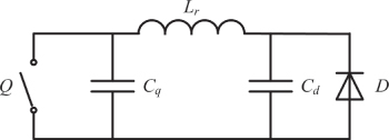
Figure 4.15 Equivalent circuit of an ZV MRS
Applying the concept of ZV MRS to the Buck converter, a Buck ZVS MR converter can be obtained, as in Figure 4.16, where Dq is the parasitic or anti-parallel diode of Q.

Figure 4.16 Schematic diagram of a Buck ZVS MR converter
4.3.1 Normal Operating Mode of Buck ZVS MR Converter
Before analyzing the operating principle of the Buck ZVS MR converter, the following assumptions are made.
- All the components in the Buck ZVS MR converter can be regarded as ideal, that is, all parasitic resistances are zero, and the conduction voltage drop is also zero.
- The filter inductance is much larger than the resonant inductance,
 .
. - The output side can be considered as a constant current source Io, because the filter inductance is very large.
The typical waveforms of a Buck ZVS MR converter in normal operating mode are illustrated in Figure 4.17. It is found that there are four stages in one switching cycle, and the equivalent circuits of operating stages are shown in Figure 4.18.
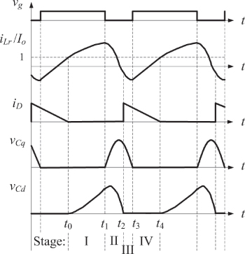
Figure 4.17 Typical waveforms of a Buck ZVS MR converter in normal operating mode
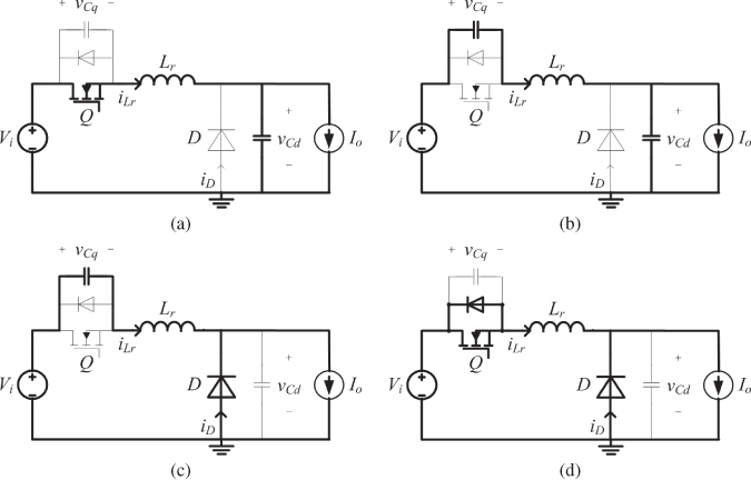
Figure 4.18 Equivalent circuits of a Buck ZVS MR converter in normal operating mode: (a) stage I; (b) stage II; (c) stage III; and (d) stage IV
Stage I (t0, t1)
As shown in Figure 4.18a, switch Q is conducting, diode D is reverse biased because vCd is always positive, and Lr resonates with Cd during stage I.
It is known that the initial conditions of stage I are ![]() ,
, ![]() , and
, and ![]() , and the expressions of iLr, vCq, and vCd during stage I can be given by
, and the expressions of iLr, vCq, and vCd during stage I can be given by
where ![]() and
and ![]() .
.
Stage II (t1, t2)
As shown in Figure 4.18b, when switch Q is turned off at t1, Cq and Cd begin resonance with Lr. Q operates in zero-voltage turn-off as the voltage vCq rises from zero slowly. iLr, vCq, and vCd can be given by


where ![]() ,
, ![]() , and
, and ![]() .
.
Stage II terminates when vCd reduces to zero at t2, and diode D turns on under zero-voltage.
Stage III (t2, t3)
As shown Figure 4.18c, since switch Q is off and diode D is on, Cq is resonant with Lr. The expressions of iLr, vCq, and vCd during stage III are
where ![]() and
and ![]() .
.
When vCq decreases to zero at t3, stage III is ended, and Dq is turned on. As a result, switch Q can be turned on with the zero-voltage condition.
Stage IV (t3, t4)
As shown in Figure 4.18d, when the converter enters into stage IV, diodes D and Dq keep conducting as a result of ![]() and
and ![]() . The voltage on the resonant inductor Lr is equal to input voltage Vi, so iLr will increase linearly. The expressions of iLr, vCq, and vCd during stage IV are
. The voltage on the resonant inductor Lr is equal to input voltage Vi, so iLr will increase linearly. The expressions of iLr, vCq, and vCd during stage IV are
Switch Q should be turned on before iLr becomes positive, or zero-voltage turn on cannot be achieved. At the moment of t4, ![]() , diode D is turned off naturally and iLr flows through switch Q, and stage IV is followed by stage I.
, diode D is turned off naturally and iLr flows through switch Q, and stage IV is followed by stage I.
Based on the above analysis, except for the operating stage IV, the other three stages operate in resonance, and the resonant frequency varies in every stage because the resonant elements are different. Therefore, this converter is known as a MR converter.
4.3.2 Sneak Circuit Phenomenon of Buck ZVS MR Converter
If circuit parameters or operating conditions of the Buck ZVS MR converter are changed, vCq reduces to zero before vCd during stage II, then a new operating stage III′, which is the sneak stage, will appear and its equivalent circuit is illustrated in Figure 4.19. During stage III′, when vCq reduces to zero at t2, Dq is turned on, then Cd will resonate with Lr. When vCd reduces to zero, stage III′ will finish and the converter will enter the normal operating stage IV. The typical waveforms of the Buck ZVS MR converter in sneak circuit mode are illustrated in Figure 4.20.
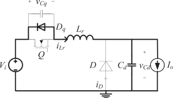
Figure 4.19 Equivalent circuit of the sneak stage in a Buck ZVS MR converter

Figure 4.20 Typical waveforms of a Buck ZVS MR converter in sneak circuit mode
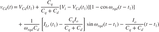
Based on Equations 4.42 and 4.43, the sneak circuit conditions at which stage III′ will appear can be expressed as
where ![]() , d is duty ratio, and T is the switching cycle.
, d is duty ratio, and T is the switching cycle.
When sneak circuit phenomenon occurs, it is found that both switch Q and diode D can keep zero-voltage turn-on, although the resonant stage is different from normal operation. But the output voltage, the voltage and current stresses of the components may change and have unpredictable influences.
4.3.3 Simulation Verification of Buck ZVS MR Converter
In order to demonstrate the correctness of the above-mentioned analysis, a Buck ZVS MR prototype based on reference [3] was built in PSIM® and the simulation parameters were ![]() ,
, ![]() ,
, ![]() ,
, ![]() ,
, ![]() , and
, and ![]() . By changing the switching frequency fs or load resistance RL, the driving voltage vgs for switch Q, resonant inductor current iLr, and resonant capacitor voltages vCq and vCd, are illustrated in Figure 4.21, which is consistent with the experimental waveforms in reference [3].
. By changing the switching frequency fs or load resistance RL, the driving voltage vgs for switch Q, resonant inductor current iLr, and resonant capacitor voltages vCq and vCd, are illustrated in Figure 4.21, which is consistent with the experimental waveforms in reference [3].

Figure 4.21 Simulation waveforms of a Buck ZVS MR prototype: (a)  ,
,  ; (b)
; (b)  ,
,  ; and (c)
  ,
, 
In Figure 4.21a, vCd reduces to zero earlier than vCq, which satisfies Figure 4.17. It is obvious that the Buck ZVS MR converter operates in normal operating mode. Figure 4.21b illustrates the critical mode that vCd and vCq decrease to zero simultaneously. However, vCq decreases to zero earlier than vCd in Figure 4.21c, which is the same as the sneak circuit phenomenon in Figure 4.20.
Comparing Figures 4.21a–c, it is proven that sneak circuit phenomenon will occur by changing the switching frequency or load resistance, which demonstrates the correctness of the above analysis.
4.4 Sneak Circuits of Buck ZVT PWM Converter
In QR converters and MR converters, both resonant inductor and resonant capacitor are involved in the process of energy transfer, and their voltage and current stresses are large as a result. In ZVS PWM converters and ZCS (zero-current switching) PWM converters, resonant inductor is in series with the main power circuit, and the voltage and current stress of switches and resonant devices are also large. In order to overcome the above shortcomings, a zero-voltage-transition (ZVT) converter was proposed in the early 1990s [4]. In this kind of converter, the resonant tank is in parallel with the main switch, and the resonant time is controlled by the auxiliary switch. Thus, the ZVT converter has the following advantages:
- All of the switching components can achieve ZVS.
- The main circuit for power transmission does not contain resonant elements. As a result, the voltage and current stresses of the main circuit are relatively small.
- The constant frequency characteristic of PWM converter can be retained
- Compared with other kinds of soft switching converters, the range of supply voltage and load resistance in zero switching loss is broadened.
As there is a resonant tank in the ZVT converter, it is likely that sneak circuit paths exist in the ZVT converter. The Buck ZVT PWM converter shown in Figure 4.22 will be used as an example to discuss the sneak circuit phenomena in a ZVT converter.

Figure 4.22 Schematic diagram of a Buck ZVT PWM converter
4.4.1 Normal Operating Mode of Buck ZVT PWM Converter
In the Buck ZVT PWM converter, an auxiliary switch Q1, auxiliary freewheeling diode D1, and resonant inductor Lr are added with respect to the traditional Buck converter. In addition, resonant capacitor Cr includes the parasitic capacitance of main switch Q, and Dq indicates the anti-parallel diode of switch Q. In order to simplify the analysis, the following assumptions are made.
- All the components are regarded as ideal ones.
- The current flowing through filter inductor L can be considered as constant current Io, because the filter inductance is large enough.
- The output voltage Vo remains constant, because the output capacitor C is large enough.
The typical operating waveforms of a Buck ZVT PWM converter in normal operating mode are illustrated in Figure 4.23. It is obvious that each switching cycle can be divided into eight stages, whose equivalent circuits are illustrated in Figure 4.24. The brief analysis of various operating stages is described as follows [4].

Figure 4.23 Typical waveforms of a Buck ZVT-PWM converter in normal operating mode
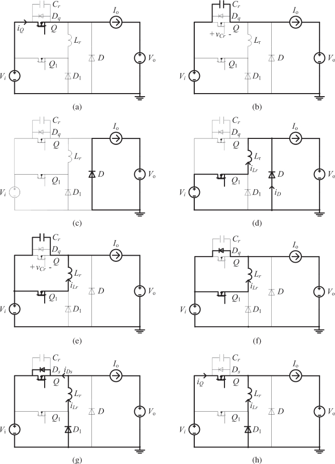
Figure 4.24 Equivalent circuits of a Buck ZVT PWM converter in normal operating mode: (a) stage I; (b) stage II; (c) stage III; (d) stage IV; (e) stage V; (f) stage VI; (g) stage VII; and (h) stage VIII
Stage I (t0, t1)
Referring to Figure 4.24a, the main switch Q is turned on and input voltage source Vi provides energy to load through Q.
Stage II (t1, t2)
Referring to Figure 4.24b, if Q is turned off at t1, Vi charges to resonant capacitor Cr, and vCr increases linearly. Stage II is ended when ![]() .
.
Stage III (t2, t3)
Referring to Figure 4.24c, as both Q and Q1 are in the off state, the current flows through the main diode D and ![]() .
.
Stage IV (t3, t4)
Referring to Figure 4.24d, the auxiliary switch Q1 is turned on at t3, iLr increases and iD decreases linearly to zero, D is turned off and stage IV is finished.
Stage V (t4, t5)
Referring to Figure 4.24e, as inductor Lr is resonant with resonant capacitor Cr. When vCr decreases to zero, Dq is turned on. Then vCr is clamped to zero, which creates the zero-voltage turn-on condition for Q.
Stage VI (t5, t6)
Referring to Figure 4.24f, iLr remains constant because the voltage across Lr is equal to zero. In this stage, Q can be turned on in zero voltage, but the current will not flow through Q until Q1 is turned off and iLr decreases to Io.
Stage VII (t6, t7)
Referring to Figure 4.24g, if Q1 is turned off at t6 and the auxiliary diode D1 is turned on, which provides a freewheeling path iLr. iLr begins to decrease and stage VII is finished until iLr decreases to Io.
Stage VIII (t7, t8)
Referring to Figure 4.24h, if ![]() at t7, iQ will increase from zero and iLr will decrease linearly. Stage VIII will terminate until iLr reduces to zero and one switching cycle is ended.
at t7, iQ will increase from zero and iLr will decrease linearly. Stage VIII will terminate until iLr reduces to zero and one switching cycle is ended.
4.4.2 Sneak Circuit Phenomenon of Buck ZVT PWM Converter
The auxiliary switch Q1 normally contains parasitic capacitance Cq1, and the Buck ZVT PWM converter with parasitic parameters is shown in Figure 4.25 [4]. When the capacitance of Cq1 cannot be ignored, Cq1 will construct a new current path with resonant inductor Lr and resonant capacitor Cr, and provide a reverse current path for iLr. As a result, sneak circuit phenomenon will appear, and the corresponding operation can be described as follows.

Figure 4.25 Schematic diagram of a Buck ZVT PWM with parasitic parameters
Stage (t0, t1)
The main switch Q conducts, iLr equals to zero, and the input voltage source Vi provides energy to load through Q, which is the same as the normal stage I.
Stage (t1, t2)
If Q is turned off at t1, and the auxiliary switch Q1 is still off at this time, Vi charges to Cr and Cq1 synchronously and iLr decreases. The equivalent circuit of this stage, which is named as stage I′, is illustrated in Figure 4.26a. Stage I′ will be finished when vCr increases to Vi.

Figure 4.26 Equivalent circuits of the sneak stages in a Buck ZVT PWM converter: (a) stage I′; (b) stage II′; (c) stage III′; and (d) stage IV′
Stage (t2, t3)
Diode D is turned on when the voltage across it is positive, and then D1 is also turned on, then the output current flows through D and the series branch D1 and Lr. The equivalent circuit of this stage, which is named as stage II′, is illustrated in Figure 4.26b. iLr keeps constant as the voltage across Lr is equal to zero.
Stage (t3, t4)
Assuming that Q1 is turned on at t3 and D1 is turned off under negative voltage, this stage is the same as normal stage IV. iLr increases linearly and iD decreases linearly, D is turned off when ![]() , and this stage is ended.
, and this stage is ended.
Stage (t4, t5)
Assuming that D is turned off at t4, this stage is the same as normal stage V. Resonant inductor Lr is resonant with resonant capacitor Cr, then vCr decreases and iLr increases in a sinusoidal way. When vCr decreases to zero and Dq is turned on, this stage is ended.
Stage (t5, t6)
This stage is the same as normal stage VI, in which the main switch Q can achieve zero voltage turn-on.
Stage (t6, t7)
Assuming that Q1 is turned off and D1 is turned on at t6, this stage is the same as normal stage VII, which will be terminated when iLr reduces to Io.
Stage (t7, t8)
This stage is the same as normal stage VIII. iQ increases from zero linearly and iLr keeps decreasing at this stage. This stage will be ended when iLr reduces to zero and D1 is turned off.
Stage (t8, t9)
The resonant inductor current iLr keeps decreasing because Lr resonates with Cq1. The equivalent circuit of this stage, which is named as stage III′, is illustrated in Figure 4.26c. This stage will be ended when the voltage on Cs1 decreases to zero and Dq1 is turned on.
Stage (t9, t10)
Assuming that Dq1 is turned on at t9, the equivalent circuit of this stage, which is named as stage IV′, is illustrated in Figure 4.26d. Because the voltage across Lr is equal to the voltage drop on Q, iLr increases linearly and this stage ends when iLr is equal to zero. Then the converter enters stage I again and another operating cycle begins.
The corresponding waveforms are illustrated in Figure 4.27a, in which the resonant inductor current iLr is discontinuous. If iLr does not increase to zero before the main switch Q is turned off, stage I will not appear in the operating process, so stage I′ will follow stage IV′ directly and iLr becomes continuous. The corresponding waveforms are illustrated in Figure 4.27b.

Figure 4.27 Typical waveforms of a Buck ZVT-PWM converter in sneak circuit mode: (a) iLr is discontinuous; and (b) iLr is continuous
Comparing the waveforms in Figure 4.27 with those in Figure 4.23, the characteristics of the Buck ZVT PWM converter change obviously when the sneak circuit phenomenon occurs. Because the parasitic capacitance of the auxiliary switch Q1, that is, Cq1, cannot be ignored, there is internal commutation during operation, which will increase the conduction loss of the main switch; on the other hand, the turn-on time of D1 (stage II′) is increased, which will lead to the efficiency drop.
4.4.3 Simulation Verification of Buck ZVT PWM Converter
In order to demonstrate the correctness of the above analysis, a simulation circuit of a Buck ZVT PWM converter was designed in PSIM® based on Figure 4.25. If Power MOSFET IRF460 was selected for the auxiliary switch, then ![]() and the other parameters were
and the other parameters were ![]() ,
, ![]() ,
, ![]() ,
, ![]() ,
, ![]() ,
, ![]() , and
, and ![]() .
.
Simulation waveforms are illustrated in Figure 4.28, from top to bottom of the figure, there are driving signal of main switch Q (i.e. v1), driving signal of auxiliary switch Q1 (i.e. v2), resonant capacitor voltage vCr, output voltage Vo, and resonant inductor current iLr. It can be observed that iLr is continuous, which is the same as that in Figure 4.27b and the correctness of sneak circuit phenomenon is proven.

Figure 4.28 Simulation waveforms of a Buck ZVT PWM converter in sneak circuit phenomenon
4.5 Summary
This chapter introduced some sneak circuit phenomena in soft-switching converters, and took FB ZVS PWM converter, Buck ZVS MR converter, and Buck ZVT PWM converter as examples. Compared with the hard-switching converter, it can be concluded that the amount of sneak circuit paths are more and the sneak circuit phenomena are more complex in the soft-switching converters because of the resonant tank. So the sneak circuit phenomenon of soft-switching converters should be avoided, or it will lead to the unpredicted influence on the converter.
References
- [1] Sabate, J.A., Vlatkovic, V., Ridely, R. et al. (1990) Design considerations for high-power full-bridge ZVS-PWM converter. IEEE Applied Power Electronic Conference Proceeding, pp. 275–284.
- [2] Tabisz, W.A. and Lee, F.C. (1989) Zero-voltage-switching multi-resonant technique- a novel approach to improve performance of high-frequency quasi-resonant converters. IEEE Transactions on Power Electronics, 4 (4), 450–458.
- [3] Tabisz, W.A. and Lee, F.C. (1989) DC analysis and design of zero-voltage-switched multi-resonant converters. IEEE Power Electronics Specialists Conference Proceedings (PESC), pp. 243–251.
- [4] Hua, G., Leu, C., Jiang, Y. et al. (1994) Novel zero-voltage-transition PWM converters. IEEE Transactions on Power Electronics, 9 (2), 213–219.