Chapter 2
Sneak Circuits of Resonant Switched Capacitor Converters
2.1 Introduction
The switched capacitor (SC) converters are one kind of power electronic converters that do not require any inductor or transformer, only using capacitors as the energy storage components [1, 2]. With the advantages of small volume, low weight, high efficiency, and easy integration, SC converters can adapt to the developing trend of power electronics. However, the SC converter has inherent disadvantages of high current stress and EMI (Electro Magnetic Interference) problem [3, 4]. In order to improve the performance of SC converters, a new topology named the resonant switched capacitor (RSC) converter has been proposed, in which an inductor is added in series with the SC [5, 6]. The inserted inductor is very small, mainly used to make up an LC resonant tank with the SC and realize zero-current switching (ZCS) for all switches. Thus, the power dissipation and EMI will be reduced and the advantages of the SC converter will be kept in RSC converters.
Compared with the SC converter, only one component is added in the RSC converter, but it is found that some new circuit paths (i.e., sneak circuits) do exist in RSC converters [7]. In this chapter, different types of sneak circuit phenomena in RSC converters will be introduced and the operating conditions of a sneak circuit will be described in detail.
2.2 Sneak Circuits of Basic RSC Converter
The elementary unit of a RSC converter is composed of two switching devices (S1 and S2), two diodes (D1 and D2), one SC Cr, and one resonant inductor Lr, as shown in Figure 2.1a. By connecting the four ports of the elementary RSC unit in different ways, step-down, step-up, and inverting RSC units can be obtained, which are shown in Figure 2.1b–d respectively.
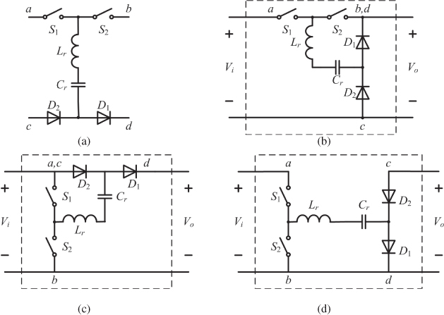
Figure 2.1 Structure of basic RSC units: (a) elementary; (b) step-down; (c) step-up; and (d) inverting
2.2.1 Sneak Circuits of Basic Step-Down RSC Converter
Based on the step-down RSC unit in Figure 2.1b, the basic step-down RSC converter is shown in Figure 2.2. The control switches used in the RSC converter, such as Power MOSFET (metal oxide semiconductor field effect transistor) and IGBT (insulated gate bipolar transistor), have the normal inverse conduction characteristics, then an anti-parallel diode can be added in parallel with the switch.

Figure 2.2 Basic step-down RSC converter
2.2.1.1 Normal Operating Mode of Basic Step-Down RSC Converter
In the normal operating mode, S1 and S2 are turned on in turn with the same duty ratio, and the switching frequency fs must be smaller than the resonant frequency ![]() (i.e.,
(i.e., ![]() ) to ensure ZCS of switches and diodes. Figure 2.3 shows the typical waveforms of driving signals vg1 for S1 and vg2 for S2, inductor current iL, and SC voltage vC.
) to ensure ZCS of switches and diodes. Figure 2.3 shows the typical waveforms of driving signals vg1 for S1 and vg2 for S2, inductor current iL, and SC voltage vC.

Figure 2.3 Typical waveforms of basic step-down RSC converter in the normal operating mode ( )
)
Assuming that all the components are ideal, both the on-state resistance of the switch and the voltage drop of the diode are ignored, the output capacitor Co is large enough to obtain a nearly constant instantaneous output voltage Vo. As shown in Figure 2.3, the normal operating process of the basic step-down RSC converter can be divided into four stages, and the corresponding equivalent circuits are demonstrated in Figure 2.4a–c, where stages II and IV are the same.

Figure 2.4 Equivalent circuits of basic step-down RSC converter in normal operating mode: (a) equivalent circuit of stage I; (b) equivalent circuit of stage II or IV; and (c) equivalent circuit of stage III
Stage I (t0, t1)
S1 and D1 are turned on with zero-current at ![]() , and Cr is charged by input voltage source Vi. Based on Figure 2.4a, the circuit equation of stage I and its solutions are
, and Cr is charged by input voltage source Vi. Based on Figure 2.4a, the circuit equation of stage I and its solutions are
where ![]() is the value of the SC voltage at
is the value of the SC voltage at ![]() , resonant angular frequency
, resonant angular frequency ![]() , and characteristic impedance
, and characteristic impedance ![]() .
.
Assuming that ![]() at
at ![]() , at that time the charging process of Cr is finished and vC increases to its maximum value VCmax, which is
, at that time the charging process of Cr is finished and vC increases to its maximum value VCmax, which is
Stage II (t1, t2)
As shown in Figure 2.4b, all the switching components are off because iL is equal to zero, and vC remains at its maximum value VCmax, that is, ![]() . The output capacitor Co discharges to the load resistor RL.
. The output capacitor Co discharges to the load resistor RL.
Stage III (t2, t3)
S2 and D2 are turned on with zero-current at ![]() and Cr is discharged to the load. Based on Figure 2.4c, the circuit equation of stage III and its solutions are
and Cr is discharged to the load. Based on Figure 2.4c, the circuit equation of stage III and its solutions are
Similarly, when ![]() ,
, ![]() , then the discharging process of Cr is finished and vC decreases to its minimum value VCmin, which is
, then the discharging process of Cr is finished and vC decreases to its minimum value VCmin, which is
Stage IV (t3, t4)
As all the switching devices are off and vC is kept at its minimum value VCmin, that is, ![]() , then, Equation 2.4 becomes
, then, Equation 2.4 becomes
From Equations 2.8 and 2.9, we obtain
Equation 2.10 shows that the relationship of input voltage and output voltage of a basic step-down RSC converter in the normal operating mode is fixed and determined by the converter structure only, which is the same as the traditional RC converter.
2.2.1.2 Sneak Circuit Mode of Basic Step-Down RSC Converter
With the same control strategy, if the inductor current iL does not stop immediately after a half resonant cycle, and keeps resonating to the inverting direction as shown in Figure 2.5, there must be some new current paths appearing in the converter operation [8].

Figure 2.5 Typical waveforms of basic step-down RSC converter in sneak circuit mode ( )
)
By analyzing the structure of the basic step-down RSC converter in Figure 2.2, it is the anti-parallel diode of the switch (e.g., DS1 of S1 or DS2 of S2), which consists of the freewheeling current path of iL. As we know, DS1 and DS2 do not participate in the converter operation in the normal operating mode, therefore the current path with DS1 or DS2 belongs to the sneak circuit path of the basic step-down RSC converter.
As shown in Figure 2.5, when ![]() is selected to ensure ZCS, the operating process of the basic step-down RSC converter includes six stages when the sneak circuit appears, where stages I, II, III, and IV are the same as those in the normal operating mode; the other two (stages I′ and III′) are with sneak circuit paths and their corresponding equivalent circuits are shown in Figure 2.6a,b respectively.
is selected to ensure ZCS, the operating process of the basic step-down RSC converter includes six stages when the sneak circuit appears, where stages I, II, III, and IV are the same as those in the normal operating mode; the other two (stages I′ and III′) are with sneak circuit paths and their corresponding equivalent circuits are shown in Figure 2.6a,b respectively.

Figure 2.6 Equivalent circuits of basic step-down RSC converter in sneak circuit mode: (a) equivalent circuit of stage I′; and (b) equivalent circuit of stage III′
The operating stages of a basic step-down RSC converter under sneak circuit mode are analyzed as follows:
Stage I (t0, t1)
S1 is turned on, and the operating process is the same as that in normal conditions, and Equations 2.1–2.4 become available.
Stage I′ (t1, t2)
As the inductor current iL continues to resonate in the negative direction, D1 is inverting biased, but DS1 and D2 are forward biased with zero-current, which means that the energy stored in the SC Cr is fed back to the input power source, and the capacitor voltage vC drops at this stage. Based on Figure 2.6a, the circuit equation of stage I′ is
As ![]() and
and ![]() , the inductor current and the capacitor voltage of this stage can be expressed as
, the inductor current and the capacitor voltage of this stage can be expressed as
When ![]() , the resonance process is finished and
, the resonance process is finished and ![]() , so the SC voltage is
, so the SC voltage is
Stage II (t2, t3)
All the switching devices are turned off and vC keeps at vC(t2).
Stage III (t3, t4)
S2 is turned on, and the operating process is the same as that in normal conditions, and Equations 2.1–2.4 are still available.
Similar to Equation 2.8, the SC voltage at ![]() is
is
Stage III′ (t4, t5)
As the inductor current iL continues to resonate in the positive direction, D2 is inverting biased, but DS2 and D1 are forward biased with zero-current, which means that the energy in resonant inductor Lr is transferred to the SC Cr, then vC rises at this stage. Based on Figure 2.6a, the circuit equation of stage III′ and its solutions are
At ![]() , the resonance is finished and
, the resonance is finished and ![]() , then
, then
Stage IV (t5, t6)
All the switching devices are off and vC remains at vC(t5), therefore
Ignoring any power loss and considering energy conservation, the input energy of the power source is equal to the consumed energy of load resistor in one switching cycle, that is

Substituting Equations 2.2 and 2.12 into the above equation, we obtain
Substituting Equations 2.14 and 2.20 into Equation 2.22, then
Based on Equation 2.15, the relationship between VCmax and VCmin is
Substituting Equation 2.24 into Equation 2.23, the output voltage is
It is obvious that the average output voltage of the basic step-down RSC converter in sneak circuit mode is related to converter parameters (such as RL and Cr) and operating conditions (such as Vi and fs), which is very different from that in normal mode, thus the sneak circuit leads to an unexpected performance.
2.2.1.3 Sneak Circuit Conditions of Basic Step-Down RSC Converter
The precondition of sneak circuit phenomena is that there is a sneak circuit path existing in the converter. In the basic step-down RSC converter, S1 and D1, DS1 (the anti-parallel diode of S1) and D2 constitute bi-directional current paths for the inductor current iL. In the normal operating mode, iL flows through the circuit path with S1 and D1 only. When sneak circuit phenomenon appears, iL flows through not only the circuit path with S1 and D1 but also the one with DS1 and D2. Therefore, the occurrence of the sneak circuit can be derived from the condition that the current flowing through the sneak path is not equal to zero.
Based on the inductor current expressions in stages I′ and III′, that is, Equations 2.12 and 2.17, the sneak circuit will appear when the following equation is satisfied:
According to Equation 2.24 and combining the above two inequalities, we have
Substituting Equation 2.25 into Equation 2.27, the sneak circuit condition of a basic step-down RSC converter can be obtained, which is
If some disturbances that make Equation 2.28 satisfied, sneak circuit phenomena will appear. Otherwise, the converter will operate in the desired way.
2.2.1.4 Experimental Verification of Basic Step-Down RSC Converter
In order to verify the above analysis, a prototype of a basic step-down RSC converter is constructed based on Figure 2.1. IRFZ44N is selected for the switch and S3SC4M is selected for the fast recovery diode. The parameters of prototype are ![]() ,
, ![]() ,
, ![]() ,
, ![]() ,
, ![]() , and
, and ![]() . Based on Equation 2.28, the sneak circuit condition of the prototype is
. Based on Equation 2.28, the sneak circuit condition of the prototype is ![]() .
.
The experimental waveforms of iL and vC at ![]() are shown in Figure 2.7a, which is consistent with the ideal ones in Figure 2.2 and prove that the prototype is working in normal operating mode. When the load is changed to
are shown in Figure 2.7a, which is consistent with the ideal ones in Figure 2.2 and prove that the prototype is working in normal operating mode. When the load is changed to ![]() , and the experimental waveforms can be obtained as in Figure 2.7b, it is obvious that the sneak circuit phenomena appear and the correctness of sneak circuit conditions has been confirmed.
, and the experimental waveforms can be obtained as in Figure 2.7b, it is obvious that the sneak circuit phenomena appear and the correctness of sneak circuit conditions has been confirmed.

Figure 2.7 Experimental waveforms of basic step-down RSC prototype under different load resistance: (a)  ; and (b)
2.2.2 Sneak Circuits of Basic Step-Up RSC Converter
2.2.2.1 Normal Operating Mode of Basic Step-Up RSC Converter
The basic step-up RSC converter is illustrated in Figure 2.8. As the value of output capacitor Co is large enough, the output side can be regarded as a DC voltage source Vo. Hence, the waveforms and equivalent circuits of the basic step-up RSC converter in the normal operating mode are shown in Figure 2.9.

Figure 2.8 Basic step-up RSC converter

Figure 2.9 Waveforms and equivalent circuits of basic step-up RSC converter in normal operating mode ( )
)
Ignoring the loss of devices, the normal operating process of the basic step-up RSC converter can be divided into four stages in the steady state.
Stage I
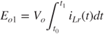
S1 and D1 are turned on with zero-current, SC Cr is charged by the input voltage source Vi, and only the output capacitor Co provides energy to the load resistor RL. The input energy to the converter at this stage is

Stage II
At this stage, the inductor current is zero. Meanwhile, all the switching devices are turned off, and Co keeps discharging to RL.
Stage III
S2 and D2 are turned on with ZCS, and Vi and Cr provide energy to RL simultaneously. The input energy to the converter at this stage is

and the output energy to the load at this stage is

Stage IV
The operating process is the same as that in Stage II.
As the resonant inductor Lr is in series with the SC Cr, equating the integral of the capacitor current (i.e., iL) over one switching period to zero yields
Based on the principle of energy conservation, we have
Substituting Equations 2.29–2.32 into Equation 2.33, the average output voltage is
It is obvious that the output voltage of a basic step-up RSC converter in normal operating mode is fixed and determined by the converter structure only, which is the same as the traditional RC converter.
2.2.2.2 Sneak Circuit Mode of Basic Step-Up RSC Converter
Referring to the sneak circuit phenomena of the basic step-down RSC converter described in Section 2.1.1, the anti-parallel diodes DS1 and DS2 in the basic step-up RSC converter can also comprise sneak circuit paths, which are shown in Figure 2.10 [9].

Figure 2.10 Sneak circuit paths of basic step-up RSC converter. (a) Sneak circuit path with DS1 and (b) sneak circuit path with DS2
If these two sneak circuit paths participate in the converter operation, then the inductor current iL can flow bi-directionally. Thus, the typical waveforms and equivalent circuits of a basic step-up RSC converter in sneak circuit mode are shown in Figure 2.11, and the operation process can be divided into six stages.

Figure 2.11 Typical waveforms and equivalent circuits of basic step-up RSC converter in sneak circuit mode ( )
)
Stage I (t0, t1)
This stage is the same as that in the normal operating mode. The expression of the inductor current is
Based on the equivalent circuit of stage I and Equation 2.35, the maximum value of the SC voltage can be obtained at the end of this stage, that is
Stage I′ (t1, t2)
The inductor current keeps resonating in the negative direction, through the circuit path Lr-Cr-D2-Vo-DS1. The inductor current at this stage is expressed by
Based on the equivalent circuit of stage I′ and Equation 2.37, the SC voltage at the end of this stage is
Stage II (t2, t3)
This stage is the same as that in normal operating mode, and ![]() .
.
Stage III (t3, t4)
This stage is the same as that in normal operating mode, and the inductor current of this stage can be expressed by
Based on the equivalent circuit of stage III and Equation 2.39, the minimum value of the SC voltage can be obtained at the end of this stage, that is
Stage III′ (t3, t4)
The inductor current keeps resonating in the positive direction, through the circuit path Lr-DS2-D1-Cr. Thus the inductor current of this stage is expressed by
Based on the equivalent circuit of stage III′ and Equation 2.41, the SC voltage at the end of this stage is
Stage IV (t5, t6)
This stage is the same as that in normal operating mode, and ![]() .
.
Due to the energy provided to the load-side during stages I′ and III being equal to that consumed by the load resistor in one switching period, we obtain
Substituting Equations 2.37 and 2.39 into the above equation, we have
Therefore
From Equation 2.45, the basic step-up RSC converter demonstrates an unexpected characteristic in sneak circuit mode, because its average output voltage Vo no longer remains at 2Vi, but relates to circuit parameters (such as Cr) and operating conditions (such as RL, fs).
2.2.2.3 Sneak Circuit Conditions of Basic Step-Up RSC Converter
Based on the above analysis, it is clear that the paths constituted by DS1 and D1, DS2, and D2 belong to the sneak circuit paths of a basic step-up RSC converter, then for the sneak circuit conditions, it can be considered that the inductor current of stages I′ and III′ are not equal to zero. From Equations 2.37 and 2.41, we know that ![]() and
and ![]() , that is
, that is
Rearranging the above inequality, we have
Substituting Equations 2.40 and 2.45 into Equation 2.47, the sneak circuit condition of a basic step-up RSC converter is
Therefore, if the circuit parameters and operation conditions of a basic step-up RSC converter do not satisfy Equation 2.48, the converter will operate normally. Otherwise, if there is a disturbance such as load RL decreasing to satisfy Equation 2.48, then sneak circuit phenomenon will appear.
2.2.2.4 Experimental Verification of Basic Step-Up RSC Converter
To verify the above analysis, a basic step-up RSC prototype is built based on Figure 2.8. IRFZ44N and S3SC4M are selected to be the switch and fast recovery diode respectively. The parameters of prototype are listed as ![]() ,
, ![]() ,
, ![]() ,
, ![]() ,
, ![]() , and
, and ![]() . Based on Equation 2.48, the sneak circuit condition of the prototype is
. Based on Equation 2.48, the sneak circuit condition of the prototype is ![]() .
.
The experimental waveforms of inductor current iL and SC voltage vC at ![]() are shown in Figure 2.12a, from which it is clear that the prototype is working in normal operating mode. The experimental waveforms at
are shown in Figure 2.12a, from which it is clear that the prototype is working in normal operating mode. The experimental waveforms at ![]() are shown in Figure 2.12b, which is different from Figure 2.12a and ensures that the sneak circuit phenomena appear.
are shown in Figure 2.12b, which is different from Figure 2.12a and ensures that the sneak circuit phenomena appear.

Figure 2.12 Experimental waveforms of basic step-up RSC prototype under different load resistance: (a)  ; and (b)
Therefore, the experimental results are consistent with the above theoretical analysis. It should be stated that the input power source is not ideal and contains internal resistance, which leads to some difference between experimental waveforms and theoretical waveforms.
2.2.3 Sneak Circuits of Basic Inverting RSC Converter
The basic inverting RSC converter is shown in Figure 2.13, which is one type of RSC converter where its output voltage is negative-polarity with respect to the common terminal of the input voltage. Normally, each switch is turned on for one half-cycle, the typical operating waveforms and equivalent circuits in normal operating mode are shown in Figure 2.14.

Figure 2.13 Basic inverting RSC converter
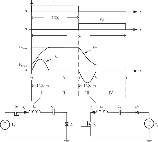
Figure 2.14 Typical waveforms and equivalent circuits of basic inverting RSC converter in normal operating mode ( )
)
It is known that the integral of capacitor current in one switching period equals zero, and from Figure 2.14, we have
Based on the principle of energy conservation, the energy provided by the input voltage source equals that sent to the load, that is
Combining Equations 2.49 and 2.50, the output voltage is
Consequently, the relationship between input and output voltages of a basic inverting RSC converter in normal operating mode is determined by the converter structure, so any disturbance in the converter parameters or operating conditions has no influence on the output voltage.
Similar to the basic step-up RSC converter, the anti-parallel diodes DS1 and DS2 could constitute the sneak circuit paths in the inverting RSC converter, which provide different paths for the inductor current. When these sneak circuit paths participate in converter operation, the typical waveforms and equivalent circuits of a basic inverting RSC converter are as shown in Figure 2.15 [9].
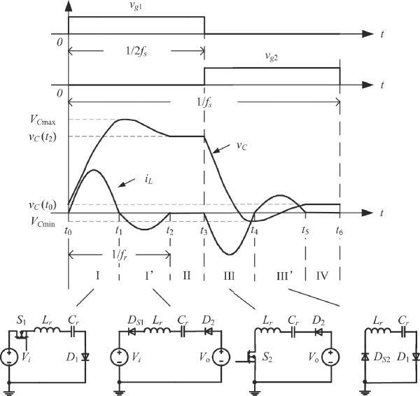
Figure 2.15 Typical waveforms and equivalent circuits of basic inverting RSC converter in sneak circuit mode ( )
)
Comparing Figure 2.15 with Figure 2.11, it is found that the equivalent circuits of a basic inverting RSC converter are similar to those of a basic step-up RSC converter when sneak circuits appear. Hence, by using the analytical method of Section 2.1.2, the output voltage of a basic inverting RSC converter in sneak circuit mode is
Therefore, when sneak circuits appear, the basic inverting RSC converter will demonstrate an unexpected characteristic, and the relationship between input and output voltages no longer keeps constant, but is determined by the circuit parameters (such as Cr) and operating condition (such as RL and fs).
Referring to Section 2.1.2, the sneak circuit condition of a basic inverting RSC converter can be derived as
A prototype of a basic inverting RSC converter was built, in which the components were the same as the basic step-up RSC prototype described in Section 2.1.2. However, the corresponding sneak circuit condition of the basic inverting RSC prototype is ![]() , based on Equation 2.53.
, based on Equation 2.53.
The experimental waveforms of SC voltage vC and inductor current iL under different loads are shown in Figure 2.16. It is found that the prototype was working in normal operating mode when ![]() , but in sneak circuit operating mode when
, but in sneak circuit operating mode when ![]() . Thus, the experimental results are consistent with the above theoretical analysis.
. Thus, the experimental results are consistent with the above theoretical analysis.

Figure 2.16 Experimental waveforms of basic inverting RSC prototype under different load resistance: (a)  ; and (b)
2.2.4 Sneak Circuit Performance of Basic RSC Converters
In order to better understand the performance of basic RSC converters, the output voltage expressions in different operating modes and the sneak circuit conditions are synthesized in Table 2.1. It can be concluded that the output voltage in sneak circuit mode is independent of the converter structure, and is closely related to circuit parameters (such as Cr) and operation conditions (such as RL and fs). As shown in Figure 2.17, the sneak circuits will lead to an unwanted performance, in which the output voltage of the basic RSC converter is usually lower than that in normal mode.
Table 2.1 Sneak circuit conditions and output voltage expressions of basic RSC converters (![]() )
)
| Converter type | Output voltage Vo | Sneak circuit condition | |
| Normal mode | Sneak circuit mode | ||
| Step-down | |
|
|
| Step-up | |
|
|
| Inverting | |
|
|
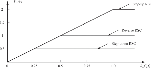
Figure 2.17  versus
  in basic RSC converters
2.3 Sneak Circuits of High-Order RSC Converter
Since the output voltage of the basic RSC converter is certain in the normal operating mode, the structure of the RSC converter has been modified to meet the requirements of larger ratio of input and output voltages.
By connecting capacitors and diodes in series or in parallel, different forms of SC units can be obtained, as shown in Figure 2.18. Commonly, the capacitance of each capacitor is equal, and the order of the SC unit (expressed as n) is defined by the number of independent capacitors in the unit. The operating principle of the SC unit is described by “charging in series and discharging in parallel,” that is, when the SC unit is charged, the independent capacitors are connected in series by the diodes between the capacitors, such as Di1 in Figure 2.18b and Di1 and Di2 in Figure 2.18c. When the SC unit is discharged, the independent capacitors are connected in parallel by other diodes, such as Dp1 and Dq2 in Figure 2.18b and Dp1, Dp2, Dq2, and Dq3 in Figure 2.18c.

Figure 2.18 SC unit: (a) n = 1; (b) n = 2; and (c) n = 3
2.3.1 Sneak Circuits of High-Order Step-Down RSC Converter
2.3.1.1 Normal Operating Mode of High-Order Step-Down RSC Converter
If the SC in the basic step-down RSC converter is replaced by a SC unit with n − 1 independent capacitors, then a n-order step-down RSC converter can be constructed, as shown in Figure 2.19 [10].
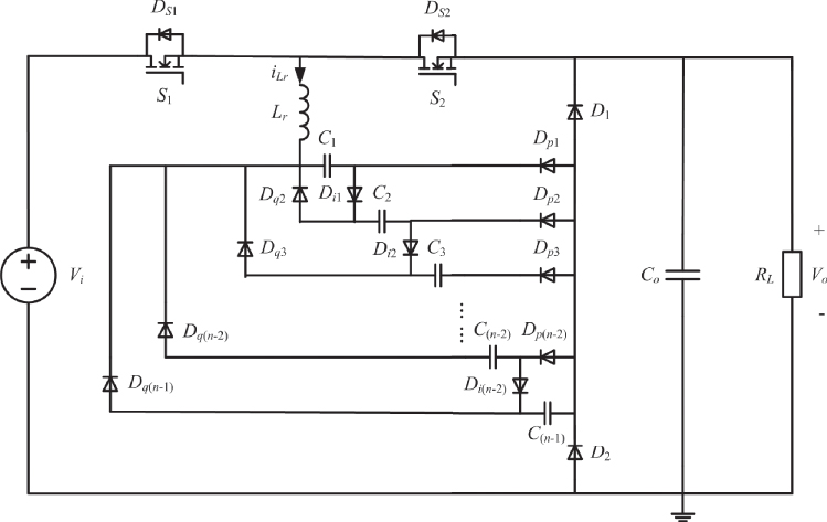
Figure 2.19 n-order step-down RSC converter
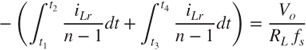
When S1 is turned on, n − 1 SCs are charged in series by the input voltage source, and the charging resonant frequency is ![]() . However, when S2 is turned on, n − 1 SCs are discharged to the load in parallel, and the discharging resonant frequency is
. However, when S2 is turned on, n − 1 SCs are discharged to the load in parallel, and the discharging resonant frequency is ![]() . In order to realize ZCS, the switching frequency fs should be smaller than the lower resonant frequency, that is,
. In order to realize ZCS, the switching frequency fs should be smaller than the lower resonant frequency, that is, ![]() .
.
According to the above operating principle of the high-order step-down RSC converter, the typical waveforms and equivalent circuits in the normal operating mode are obtained, as in Figures 2.20 and 2.21 respectively. The operating process of the converter can be divided into four stages, as all the devices are assumed ideal to simplify the analysis.

Figure 2.20 Typical waveforms of the n-order step-down RSC converter in normal operating mode ( )
)
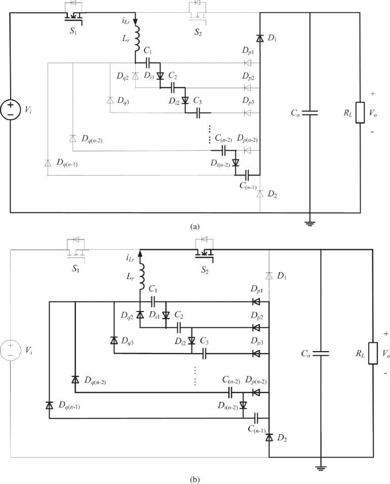
Figure 2.21 Equivalent circuits of the n-order step-down RSC converter in normal operating mode: (a) equivalent circuit of stage I; and (b) equivalent circuit of stage III
Stage I
As shown in Figure 2.21a, S1 and D1 are turned on with zero-current at ![]() , and the SCs are charged by Vi in series. Thus the capacitor current is equal to the inductor current, that is,
, and the SCs are charged by Vi in series. Thus the capacitor current is equal to the inductor current, that is, ![]() , (
, (![]() ). When
). When ![]() ,
, ![]() , the capacitor voltage vCx reaches its maximum value.
, the capacitor voltage vCx reaches its maximum value.
The input energy from the voltage source in this stage is

and the output energy to the load in this stage is
Stage II
When all the switching devices are turned off, vCx keeps at its maximum value. Only the output capacitor Co provides energy to the load resistor RL.
Stage III
When ![]() , S2 and D2 are turned on with zero-current, and the switching capacitors are discharged to the load in parallel, as shown in Figure 2.21b. When
, S2 and D2 are turned on with zero-current, and the switching capacitors are discharged to the load in parallel, as shown in Figure 2.21b. When ![]() , the capacitor voltage vCx drops to its minimum value. Based on Kirchhoff's voltage law, the state equation for each SC is
, the capacitor voltage vCx drops to its minimum value. Based on Kirchhoff's voltage law, the state equation for each SC is
Because the capacitance of each SC is selected to be equal, that is, ![]() , the derivation of Equation 2.56 is
, the derivation of Equation 2.56 is
which means that the current flowing in each SC is equal in stage III, and ![]() can be obtained from Figure 2.21b.
can be obtained from Figure 2.21b.
The output energy to the load at this stage is

Stage IV
The operating process is the same as that in stage II, but vCx keeps at its minimum value.
According to the integral of the capacitor current over one switching period being zero, the current of capacitor C1 satisfies

The energy conservation principle yields ![]() , that is
, that is

Substituting Equation 2.59 to Equation 2.60 gives
When the number of SCs in Figure 2.19 is set to ![]() (i.e.,
(i.e., ![]() ), which means that there is only one SC in the high-order step-down RSC converter, the corresponding output voltage is
), which means that there is only one SC in the high-order step-down RSC converter, the corresponding output voltage is ![]() , which is the same as that of the basic step-down RSC converter.
, which is the same as that of the basic step-down RSC converter.
From Equation 2.61, it is obvious that the relationship between input and output voltages of the high-order step-down RSC converter in the normal operating mode is decided by the topology of the converter or the number of SCs, as well as the traditional high-order SC converter [11].
2.3.1.2 Sneak Circuit Mode of High-Order Step-Down RSC Converter
According to the sneak circuit paths in basic RSC converters, the sneak circuit paths of the high-order step-down RSC converter may be composed of the anti-parallel diode of the switch, that is, DS1 or DS2, which are illustrated in Figure 2.22 [12].

Figure 2.22 Sneak circuit paths in the n-order step-down RSC converter: (a) circuit paths when Ds1 is on; and (b) circuit paths when Ds2 is on
If the sneak circuits in Figure 2.22a exist, it means that the SCs are discharged to the voltage source in parallel through DS1. As all of the SCs are charged in series by the input voltage through S1 in stage I, the voltage on every SC at the end of stage I is lower than the input voltage Vi. Therefore, the sneak circuit paths in Figure 2.22a are not in fact available.
If the sneak circuits in Figure 2.22b exist, it means that the SCs are charged in series by the resonant inductor Lr through DS2. This sneak circuit path can appear without any restriction.
The waveforms of inductor current iLr and capacitor voltage vCx of a high-order step-down RSC converter in sneak circuit mode are shown in Figure 2.23, where the operating process can be divided into five stages. Among these stages, the equivalent circuits of stages I, II, III, and IV are the same as those of normal operating mode, and the equivalent circuit of stage III′ is shown in Figure 2.22b. In addition, it is found that ZCS can be ensured when the switching frequency is satisfied by ![]() .
.

Figure 2.23 Typical waveforms of the n-order step-down RSC converter in sneak circuit mode 
Though the resonant inductor and SCs construct different series-resonant circuit paths in stages I, III, and III′, the inductor current iLr and the voltage of each SC vcx can be expressed in the unified form:

where VS is the equivalent voltage source of the series-resonant circuit, VC0 is the equivalent initial value of the SC voltage, ![]() is the equivalent resonant angular frequency,
is the equivalent resonant angular frequency, ![]() is the equivalent characteristic impedance, and knr is a constant related to the SC voltage.
is the equivalent characteristic impedance, and knr is a constant related to the SC voltage.
Based on the equivalent circuits of stages I, III, and III′, the definitions of each parameter of Equation 2.62 at different stages are summarized in Table 2.2. According to Equation 2.62 and Table 2.2, the maximum value, minimum value, and initial value of each SC can be deduced as
Table 2.2 Parameters of the n-order step-down RSC converter in sneak circuit mode
| Stage | I | III | III′ |
 |
 |
||
| 1 |
In the steady state, the energy provided to the output side equals that consumed by the load resistor in one switching cycle, that is

Substituting Equations 2.62 and 2.63 into Equation 2.64, the output voltage when the sneak circuit appears can be defined by
which is in accordance with the output voltage of the basic step-down RSC converter in sneak circuit mode, that is, Equation 2.45.
Referring to the above analysis, the inductor current of stage III′ is not equal to zero when the sneak circuit appears, which means that ![]() based on Equation 2.62 and Table 2.2, that is
based on Equation 2.62 and Table 2.2, that is
Substituting Equations 2.63 and 2.65 into Equations 2.66,
can be obtained as the sneak circuit condition of the high-order step-down RSC converter.
Compared to the sneak circuit condition of the basic step-down RSC converter, that is, Equation 2.28, Equation 2.67 can be considered as a common sneak circuit condition of the step-down RSC converter, where ![]() refers to basic step-down RSC converter.
refers to basic step-down RSC converter.
2.3.1.3 Experimental Verification of Three-order Step-Down RSC Converter
To verify the above analysis, a prototype of a three-order step-down RSC converter (n = 3), as shown in Figure 2.24, was built. As the prototype parameters were selected to ![]() ,
, ![]() ,
, ![]() ,
, ![]() ,
, ![]() ,
, ![]() , and
, and ![]() , the sneak circuit condition of the prototype is
, the sneak circuit condition of the prototype is ![]() based on Equation 2.67, and the experimental waveforms under different load are shown in Figure 2.25.
based on Equation 2.67, and the experimental waveforms under different load are shown in Figure 2.25.

Figure 2.24 The structure of a three-order step-down RSC prototype
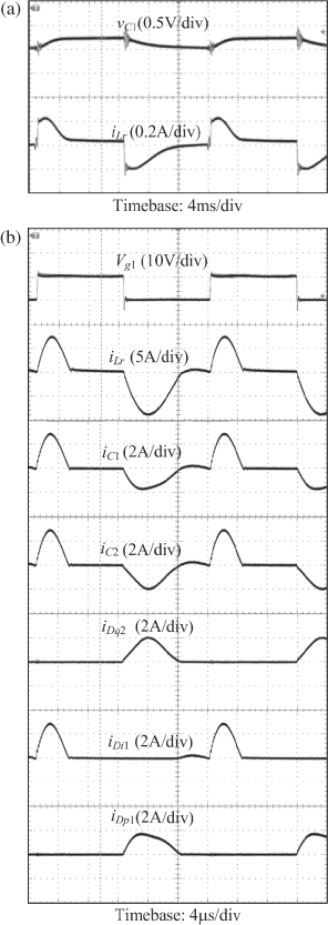
Figure 2.25 Experimental waveforms of a three-order step-down RSC prototype under different load: (a)  ; and (b)
When ![]() , the experimental waveforms of inductor current iLr and SC voltage vC1 shown in Figure 2.23a verify that the prototype is operating in the normal operating mode. Changing the load resistance to
, the experimental waveforms of inductor current iLr and SC voltage vC1 shown in Figure 2.23a verify that the prototype is operating in the normal operating mode. Changing the load resistance to ![]() , the experimental waveforms of inductor current, SC currents and diode currents, shown in Figure 2.22b, make it is clear that the sneak circuit phenomena appear at that time. Thus, the correctness of the sneak circuit paths and sneak circuit conditions has been verified.
, the experimental waveforms of inductor current, SC currents and diode currents, shown in Figure 2.22b, make it is clear that the sneak circuit phenomena appear at that time. Thus, the correctness of the sneak circuit paths and sneak circuit conditions has been verified.
2.3.2 Sneak Circuits of High-Order Step-Up RSC Converter
2.3.2.1 Normal Operating Mode of High-Order Step-Up RSC Converter
The step-up SC unit can be extracted from the basic step-up RSC converter, as shown in Figure 2.26. If several step-up SC units are connected in the form of the push-pull structure, and replace the step-up SC unit in the basic step-up RSC converter, then the high-order step-up RSC converter can be obtained, as in Figure 2.27, in which there are n − 1 step-up SC units [13].

Figure 2.26 Step-up SC unit

Figure 2.27 n-order step-up RSC converter
Based on the principle of ratio equality, S1 and S2 are switched on in turn. The normal operating process of a high-order step-up RSC converter can be divided into four stages, and its typical waveforms and equivalent circuits of each stage are shown in Figures 2.28 and 2.29 respectively. To simplify the analysis, it is assumed that all the devices are ideal devices and the capacitance of every SC is equal, that is, ![]() . In addition, because the output capacitor
. In addition, because the output capacitor ![]() (
(![]() ) is generally large, the output capacitor voltage is constant, which can be regarded as a DC voltage source, represented by
) is generally large, the output capacitor voltage is constant, which can be regarded as a DC voltage source, represented by ![]() . Each stage of the n-order step-up RSC converter in normal operating mode is analyzed as follows:
. Each stage of the n-order step-up RSC converter in normal operating mode is analyzed as follows:

Figure 2.28 Typical waveforms of the n-order step-up RSC converter in normal operating mode ( )
)
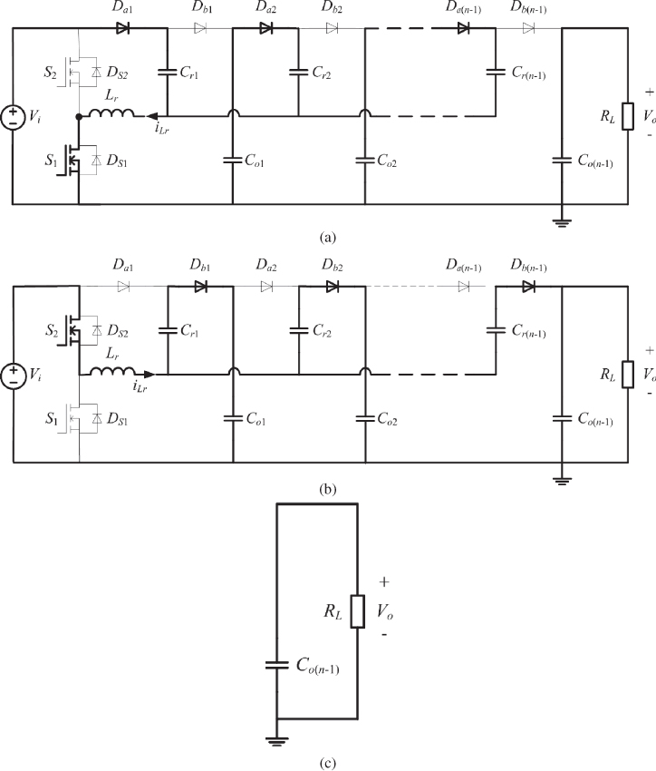
Figure 2.29 Equivalent circuits of the n-order step-up RSC converter in normal operating mode: (a) equivalent circuit of stage I; (b) equivalent circuit of stage III; and (c) equivalent circuits of stage II and IV
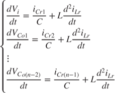
Stage I
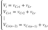
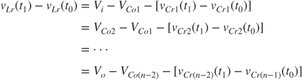
S1, Da1, Da2,…, Da(n−1) are turned on with ZCS. As shown in Figure 2.29a, Cr1 is charged by Vi, Cr2 is charged by Co1, Cr3 is charged by Co2,…, Cr(n−1) is charged by Co(n−2), and Co(n−1) supplies energy to the load resistor RL.
At ![]() ,
, ![]() , the SC voltage vCrx rises to its maximum value of
, the SC voltage vCrx rises to its maximum value of ![]() . According to Kirchhoff's voltage law, we obtain
. According to Kirchhoff's voltage law, we obtain
Differentiating the above equations, we have
Assuming that ![]() is approximate to a constant value, and its derivative equates to zero. Therefore, the current flowing through each SC is derived from Equation 2.69, which is
is approximate to a constant value, and its derivative equates to zero. Therefore, the current flowing through each SC is derived from Equation 2.69, which is
Stage II
Since the inductor current iLr remains at zero, all the switching devices are turned off, vCrx remains at its maximum value, and Co(n−1) discharges to RL.
Stage III
S2, Db1, Db2,…, Db(n−1) are also turned on with ZVS (zero voltage switching). As shown in Figure 2.29b, Co1 is charged by Vi and Cr1, Co2 is charged by Vi and Cr2,…, Co(n−1) is charged by Vi and Cr(n−1). At ![]() ,
, ![]() , vCrx decreases to its minimum value of
, vCrx decreases to its minimum value of ![]() .
.
According to Kirchhoff's voltage law, the circuit equation of stage III can be expressed by
where ![]() . Therefore, Equation 2.70 is still available in stage III.
. Therefore, Equation 2.70 is still available in stage III.
Stage IV
The converter operation is the same as that in stage II, but vCrx remains at its minimum value. As the integral of capacitor current is zero in one switching cycle, from Equation 2.70, we have

The energy conservation principle yields

Substituting Equations 2.70 and 2.72 into Equation 2.73, we obtain
where ![]() refers to the basic step-up RSC converter.
refers to the basic step-up RSC converter.
From Equation 2.74, it is known that the relationship between input and output voltages of a high-order step-up RSC converter in normal mode is decided by the converter topology, which is the number of the step-up SC unit.
2.3.2.2 Sneak Circuit Mode of High-order Step-Up RSC Converter
Similar to the basic step-up RSC converter, the sneak circuit paths of a high-order step-up RSC converter include the anti-parallel diode of switch DS1 or DS2. Based on Figure 2.27, it is obvious that there are n − 1 current paths passing through DS1, which are Lr-Cr1-Db1-Co1-DS1, Lr-Cr2-Db2-Co2-DS1,…, Lr-Cr(n−1)-Db(n−1)-Co(n−1)(RL)-DS1, highlighted in Figure 2.30a; there are n − 1 current paths passing through DS2 too, which are Lr-DS2-Da1-Cr1, Lr-DS2-Vi-Co1-Da2-Cr2, Lr-DS2-Vi-Co2-Da3-Cr3,…, Lr-DS2-Vi-Co(n−2)-Da(n−1)-Cr(n−1), highlighted in Figure 2.30b [14].

Figure 2.30 Sneak circuit paths of the n-order step-up RSC converter: (a) circuit paths when DS1 is on; and (b) circuit paths when DS2 is on
Once the above sneak circuits appear, there will be two more operating stages than the normal mode, and the corresponding waveforms are shown in Figure 2.31. In order to ensure ZCS of all switching components, ![]() is selected, then the operating process of the high-order step-up RSC converter in sneak circuit mode will be divided into six stages, and the equivalent circuit of stages I′ and III′ are referred to in Figure 2.30a,b respectively.
is selected, then the operating process of the high-order step-up RSC converter in sneak circuit mode will be divided into six stages, and the equivalent circuit of stages I′ and III′ are referred to in Figure 2.30a,b respectively.

Figure 2.31 Typical waveforms of the n-order step-up RSC converter in sneak circuit mode ( )
)
Like the analysis method described above, it can be proved that the current flowing through each SC is equal; moreover, Equation 2.70 is still effective at any stage.
Ignoring the dissipation of the switching devices, the energy sent to the load in stages I′ and III is equal to that assumed by the load resistor in one switching period, that is
Taking Cr1 as an example, the voltage difference on Cr1 is defined by

Substituting Equation 2.76 into Equation 2.75, we have
According to the equivalent circuit of stage I, that is, Figure 2.29a, the voltage of Cr1 is expressed by
where ![]() is the resonant angular frequency of the n-order step-up RSC converter.
is the resonant angular frequency of the n-order step-up RSC converter.
When ![]() ,
,
According to the equivalent circuit of stage III′, Figure 2.30b, the voltage of Cr1 is expressed by
When ![]() ,
,
Substituting Equations 2.79 and 2.81 into Equation 2.77, we obtain
When sneak circuits appear in the high-order step-up RSC converter, its output voltage is no longer decided by the converter topology, but relates to circuit parameters or operating conditions instead.
2.3.2.3 Sneak Circuit Conditions of High-Order Step-Up RSC Converter
Referring to the sneak circuit conditions of the basic step-up RSC converter, it is known that when a sneak circuit appears in a high-order step-up RSC converter, the inductor current will not be equal to zero in stages I′ or III′. Again, taking Cr1 as an example, the expressions of the SC current in stage I′ and III′ are

where ![]() is the characteristic impedance of the n-order step-up RSC converter.
is the characteristic impedance of the n-order step-up RSC converter.
Because ![]() , the sneak circuit conditions can be deduced from Equation 2.83 and Figure 2.31, which are
, the sneak circuit conditions can be deduced from Equation 2.83 and Figure 2.31, which are

Substituting Equations 2.79 and 2.81 into Equation 2.84, the inequality changes to
According to equivalent circuit of stage I in Figure 2.29a, when ![]() , the inductor voltage satisfies
, the inductor voltage satisfies
According to equivalent circuit of stage I′ in Figure 2.30a, when ![]() , the inductor voltage satisfies
, the inductor voltage satisfies

Subtracting Equation 2.83 from Equation 2.84, we have
As the current flowing through each SC is equal, we have

Therefore,
Summing up all the equations in Equation 2.90, we have
Substituting Equation 2.91 into Equation 2.85, the sneak circuit condition of high-order step-up RSC converter can be obtained:
When ![]() , the result of Equation 2.92 is consistent with Equation 2.48, which is the sneak circuit condition of the basic step-up RSC converter. Therefore, Equation 2.92 can be considered as a common sneak circuit condition of step-up RSC converters.
, the result of Equation 2.92 is consistent with Equation 2.48, which is the sneak circuit condition of the basic step-up RSC converter. Therefore, Equation 2.92 can be considered as a common sneak circuit condition of step-up RSC converters.
2.3.2.4 Experimental Verification of Three-Order Step-Up RSC Converter
To verify the above analysis, a prototype of a three-order step-up RSC converter (n = 3) was built, as shown in Figure 2.32, with parameters of ![]() ,
, ![]() ,
, ![]() ,
, ![]() ,
, ![]() , and
, and ![]() . Based on Equation 2.92, when the load resistance satisfies
. Based on Equation 2.92, when the load resistance satisfies ![]() , the sneak circuit phenomena will appear. The experimental waveforms of SC voltages and inductor current with
, the sneak circuit phenomena will appear. The experimental waveforms of SC voltages and inductor current with ![]() are shown in Figure 2.33a, which proves that the prototype is working in the normal operating mode.
are shown in Figure 2.33a, which proves that the prototype is working in the normal operating mode.

Figure 2.32 The structure of a three-order step-up RSC prototype

Figure 2.33 Experimental waveforms of a three-order step-up RSC prototype under different load; (a)  ; and (b)
By reducing the load resistance to ![]() , the sneak circuit phenomena of the prototype can be observed in Figure 2.33b. Because the input power source has certain internal resistance, and the voltage drop of diodes cannot be ignored, there are some differences in stage III′ between experimental waveforms and ideal waveforms.
, the sneak circuit phenomena of the prototype can be observed in Figure 2.33b. Because the input power source has certain internal resistance, and the voltage drop of diodes cannot be ignored, there are some differences in stage III′ between experimental waveforms and ideal waveforms.
2.4 Summary
This chapter presented the sneak circuit phenomena in families of RSC converters, and derived the expression of output voltage and the sneak circuit conditions. When the RSC converter is operating in normal mode, the relationship between the input and output voltages are only decided by the converter topology. However, when the sneak circuit appears, the output voltage will be dependent on the circuit parameters and operating conditions, and then the RSC converter will exhibit unexpected behavior. All sneak circuit conditions have been verified by the experimental results, which are useful to restrain the sneak circuit phenomena of RSC converters.
References
- [1] Singer, Z., Emanuel, A. and Erlicki, M. (1972) Power regulation by means of a switched capacitor. Proceedings of Institution of Electrical Engineers, 119 (2), 149–153.
- [2] Oota, I., Inoue, T. and Ueno, F. (1983) A realization of low-power supplies using switched-capacitor transformers and its analysis. Transactions of the Institute of Electronics and Communications Engineers of Japan, J-66C, 576–583.
- [3] Chung, H. (1999) Design and analysis of a switched-capacitor-based step-up DC/DC converter with continuous input current. IEEE Transactions on Circuits and Systems-I: Fundamental Theory and Applications, 46 (6), 722–730.
- [4] Makowski, M.S. and Maksimovic, D. (1995) Performance limits of switched capacitor DC-DC converters. Proceedings of IEEE Power Electronics Specialists Conference (PESC), vol. 2, pp. 1215–1221.
- [5] Cheng, K.W.E. (1998) New generation of switched capacitor converters. Proceedings of IEEE Power Electronics Specialists Conference (PESC), pp. 1529–1535.
- [6] Cheng, K. (2001) Zero-current-switching switched capacitor converters. IEE Proceedings of Electric Power Applications, 148 (5), 403–409.
- [7] Qiu, D. and Zhang, B. (2006) Discovery of sneak circuit phenomena in resonant switched capacitor DC-DC converters. Proceedings of IEEE Conference on Industrial Electronics and Applications (ICIEA), pp. 993–996.
- [8] Qiu, D. and Zhang, B., (2006) Analysis of step-down resonant capacitor converter with sneak circuit state. Proceedings of IEEE Power Electronics Specialists Conference (PESC), pp. 2940–2944.
- [9] Tu, W., Qiu, D., Zhang, B. et al. (2007) General laws of sneak circuit in resonant switched capacitor. Proceedings of IEEE Power Electronics Specialists Conference (PESC), pp. 708–712.
- [10] Yeung, Y., Cheng, K., Sutanto, D. et al. (2002) Zero-current switching switched-capacitor quasiresonant step-down converter. Proceedings of IEE Electric Power Applications, 149 (2), 111–121.
- [11] Yeung, Y.P.B., Cheng, K.W.E., Ho, S.L. et al. (2004) Unified analysis of switched-capacitor resonant converters. IEEE Transactions on Industrial Electronics, 51 (4), 864–873.
- [12] Li, J., Qiu, D. and Zhang, B. (2007) Sneak circuit analysis for n-stage resonant switched capacitor converters based on graph theory. Proceedings of Annual Conference of the IEEE Industrial Electronics Society (IECON), pp. 1581–1585.
- [13] Law, K., Cheng, K. and Yeung, Y. (2005) Design and analysis of switched-capacitor-based step-up resonant converters. IEEE Transactions on Circuits and Systems–II: Regular Papers, 52 (5), 943–948.
- [14] Tu, W., Qiu, D., Zhang, B. et al. (2007) Sneak circuit analysis in n-stage resonant switched capacitor converters. Proceedings of IEEE International Workshop of Anti-Counterfeiting Security, Identification (ASID), pp. 61–65.