
5
RECTIFICATION OF UTILITY INPUT USING DIODE RECTIFIERS
As discussed in the introduction to Chapter 1, the role of power electronics is to facilitate power flow, often in a controlled manner, between two systems shown in Figure 5.1: one of them a “source” and the other a “load.” Typically, power is provided by a single-phase or a three-phase utility source, for example, in adjustable-speed motor drives. (Of course, there are exceptions, for example, in wind turbines, where the wind-turbine generator is the source of power to the utility grid that acts like a “load.”)

FIGURE 5.1 Block diagram of power electronic systems.
Such power-electronic interfaces often consist of a voltage-link structure, discussed in Section 1.5.1, where the input from the AC source is first rectified into a DC voltage across a large capacitor. If reversing power flow is not an objective, it is possible to rectify the AC input, single-phase or three-phase, by means of diode rectifiers discussed in this chapter. The knowledge of such systems is essential for learning about thyristor converters, discussed in Chapter 13, which are used in important applications such as high-voltage DC transmission (HVDC) systems.
5.1 INTRODUCTION
In diode rectifiers, unless corrective action is taken as described in the next chapter, power is drawn by means of highly distorted currents, which have a deleterious effect on the power quality of the utility source. This issue and the basic principles of diode-rectifier operation are examined in this chapter.
5.2 DISTORTION AND POWER FACTOR
To quantify distortion in the current drawn by power electronic systems, it is necessary to define certain indices. As a base case, consider the linear ![]() load shown in Figure 5.2a, which is supplied by a sinusoidal source in steady state. The voltage and current phasors are shown in Figure 5.2b, where
load shown in Figure 5.2a, which is supplied by a sinusoidal source in steady state. The voltage and current phasors are shown in Figure 5.2b, where ![]() is the angle by which the current lags the voltage. Using RMS values for the voltage and current magnitudes, the average power supplied by the source is
is the angle by which the current lags the voltage. Using RMS values for the voltage and current magnitudes, the average power supplied by the source is

FIGURE 5.2 Voltage and current phasors in a simple R-L circuit.
The power factor ![]() at which power is drawn is defined as the ratio of the real average power P to the product of the RMS voltage and the RMS current:
at which power is drawn is defined as the ratio of the real average power P to the product of the RMS voltage and the RMS current:
where ![]() is the apparent power. For a given voltage, from Equation (5.2), the RMS current drawn is
is the apparent power. For a given voltage, from Equation (5.2), the RMS current drawn is
This shows that the power factor PF and the current ![]() are inversely proportional. This current flows through the utility distribution lines, transformers, and so on, causing losses in their resistances. This is the reason why utilities prefer unity power factor loads that draw power at the minimum value of the RMS current.
are inversely proportional. This current flows through the utility distribution lines, transformers, and so on, causing losses in their resistances. This is the reason why utilities prefer unity power factor loads that draw power at the minimum value of the RMS current.
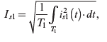
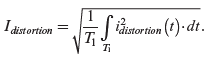
5.2.1 RMS Value of Distorted Current and the Total Harmonic Distortion (THD) [1]
The sinusoidal current drawn by the linear load in Figure 5.2 has zero distortion. However, power electronic systems with diode rectifiers as the front-end draw currents with a distorted waveform such as that shown by ![]() in Figure 5.3a. The utility voltage
in Figure 5.3a. The utility voltage ![]() is assumed sinusoidal. The following analysis is general, applying to the utility supply that is either single-phase or three-phase, in which case the analysis is on a per-phase basis.
is assumed sinusoidal. The following analysis is general, applying to the utility supply that is either single-phase or three-phase, in which case the analysis is on a per-phase basis.
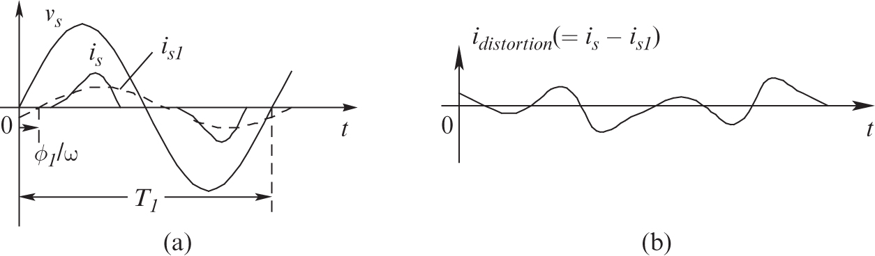
FIGURE 5.3 Current drawn by power electronics equipment with diode-bridge front-end.
The current waveform ![]() in Figure 5.3a repeats with a time period
in Figure 5.3a repeats with a time period ![]() . By Fourier analysis of this repetitive waveform, we can compute its fundamental frequency (
. By Fourier analysis of this repetitive waveform, we can compute its fundamental frequency (![]() ) component
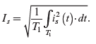
) component ![]() , shown dotted in Figure 5.3a. The distortion component
, shown dotted in Figure 5.3a. The distortion component ![]() in the input current is the difference between
in the input current is the difference between ![]() and the fundamental-frequency component
and the fundamental-frequency component ![]() :
:
where ![]() using Equation (5.4) is plotted in Figure 5.3b. This distortion component consists of components at frequencies that are the multiples of the fundamental frequency.
using Equation (5.4) is plotted in Figure 5.3b. This distortion component consists of components at frequencies that are the multiples of the fundamental frequency.
To obtain the RMS value of ![]() in Figure 5.3a, we will apply the basic definition of RMS:
in Figure 5.3a, we will apply the basic definition of RMS:
 (5.5)
(5.5)
Using Equation (5.4),
In a repetitive waveform, the integral of the products of the two harmonic components (including the fundamental) at unequal frequencies, over the repetition time-period, equals zero:
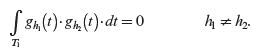 (5.7)
(5.7) Therefore, substituting Equation (5.6) into Equation (5.5) and making use of Equation (5.7) that implies that the integral of the third term on the right side of Equation (5.6) equals zero (assuming the average component to be zero),
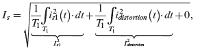 (5.8)
(5.8)
or
where the RMS values of the fundamental-frequency component and the distortion component are as follows:
 (5.10)
and
 (5.11)
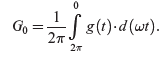
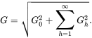
Based on the RMS values of the fundamental and the distortion components in the input current ![]() , a distortion index called the total harmonic distortion (THD) is defined in percentage as follows:
, a distortion index called the total harmonic distortion (THD) is defined in percentage as follows:
Using Equation (5.9) into Equation (5.12),
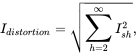
The RMS value of the distortion component can be obtained based on the harmonic components (except the fundamental) as follows using Equation (5.7):
 (5.14)
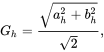
where ![]() is the RMS value of the harmonic component “h.”
is the RMS value of the harmonic component “h.”
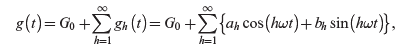
5.2.1.1 Obtaining Harmonic Components by Fourier Analysis
By Fourier analysis, any distorted (non-sinusoidal) waveform ![]() that is repetitive with a fundamental frequency
that is repetitive with a fundamental frequency ![]() , for example,
, for example, ![]() in Figure 5.3a, can be expressed as a sum of sinusoidal components at the fundamental frequency and its multiples (harmonic frequencies):
in Figure 5.3a, can be expressed as a sum of sinusoidal components at the fundamental frequency and its multiples (harmonic frequencies):
 (5.15)
where the average value ![]() is DC,
is DC,
 (5.16)
The sinusoidal waveforms in Equation (5.15) at the fundamental frequency ![]() (
(![]() ) and the harmonic components at frequencies
) and the harmonic components at frequencies ![]() times
times ![]() can be expressed as the sum of their cosine and sine components,
can be expressed as the sum of their cosine and sine components,
 (5.17)
 (5.18)
The cosine and the sine components above, given by Equations (5.17) and (5.18), can be combined and written as a phasor in terms of its RMS value,
where the RMS magnitude in terms of the peak values ![]() and
and ![]() equals
equals
 (5.20)
and the phase ![]() can be expressed as
can be expressed as
It can be shown that the RMS value of the distorted function ![]() can be expressed in terms of its average and the sinusoidal components as
can be expressed in terms of its average and the sinusoidal components as
 (5.22)
In Fourier analysis, by appropriate selection of the time origin, it is often possible to make the sine or the cosine components in Equation (5.15) to be zero, thus considerably simplifying the analysis, as illustrated by a simple example below.
A current ![]() of a square waveform is shown in Figure 5.4a. Calculate and plot its fundamental frequency component and its distortion component. What is the %THD associated with this waveform?
of a square waveform is shown in Figure 5.4a. Calculate and plot its fundamental frequency component and its distortion component. What is the %THD associated with this waveform?

Solution From Fourier analysis, by choosing the time origin as shown in Figure 5.4a, ![]() in Figure 5.4a can be expressed as
in Figure 5.4a can be expressed as
The fundamental frequency component and the distortion component are plotted in Figures 5.4b and 5.4c.
From Figure 5.4a, it is obvious that the RMS value ![]() of the square waveform is equal to
of the square waveform is equal to ![]() . In the Fourier expression of Equation (5.23), the RMS value of the fundamental-frequency component is
. In the Fourier expression of Equation (5.23), the RMS value of the fundamental-frequency component is
Therefore, the distortion component can be calculated from Equation (5.9) as
Therefore, using the definition of THD,
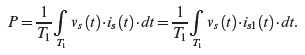
5.2.2 The Displacement Power Factor (DPF) and Power Factor (PF)
Next, we will consider the power factor at which power is drawn by a load with a distorted current waveform such as that shown in Figure 5.3a. As before, it is reasonable to assume that the utility-supplied line-frequency voltage ![]() is sinusoidal, with an RMS value of
is sinusoidal, with an RMS value of ![]() and a frequency
and a frequency ![]() . Based on Equation (5.7), which states that the product of the cross-frequency terms has a zero average, the average power P drawn by the load in Figure 5.3a is due only to the fundamental-frequency component of the current:
. Based on Equation (5.7), which states that the product of the cross-frequency terms has a zero average, the average power P drawn by the load in Figure 5.3a is due only to the fundamental-frequency component of the current:
 (5.24)
Therefore, in contrast to Equation (5.1) for a linear load, in a load that draws distorted current, similar to Equation (5.1),
where ![]() is the angle by which the fundamental-frequency current component
is the angle by which the fundamental-frequency current component ![]() lags behind the voltage, as shown in Figure 5.3a.
lags behind the voltage, as shown in Figure 5.3a.
At this point, another term called the displacement power factor (DPF) needs to be introduced, where,
Therefore, using the DPF in Equation (5.25),
In the presence of distortion in the current, the meaning and therefore the definition of the power factor, at which the real average power P is drawn, remains the same as in Equation (5.2), that is, the ratio of the real power to the product of the RMS voltage and the RMS current:
Substituting Equation (5.27) for P into Equation (5.28),
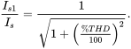
In linear loads that draw sinusoidal currents, the current-ratio ![]() in Equation (5.29) is unity, hence
in Equation (5.29) is unity, hence ![]() . Equation (5.29) shows the following: a high distortion in the current waveform leads to a low power factor, even if the DPF is high. Using Equation (5.13), the ratio
. Equation (5.29) shows the following: a high distortion in the current waveform leads to a low power factor, even if the DPF is high. Using Equation (5.13), the ratio ![]() in Equation (5.29) can be expressed in terms of the total harmonic distortion as
in Equation (5.29) can be expressed in terms of the total harmonic distortion as
 (5.30)
Therefore, in Equation (5.29),
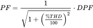 (5.31)
The effect of THD on the power factor is shown in Figure 5.5 by plotting ![]() versus THD. It shows that even if the displacement power factor is unity, a total harmonic distortion of 100% (which is possible in power electronic systems unless corrective measures are taken) can reduce the power factor to approximately 0.7 (or
versus THD. It shows that even if the displacement power factor is unity, a total harmonic distortion of 100% (which is possible in power electronic systems unless corrective measures are taken) can reduce the power factor to approximately 0.7 (or ![]() , to three decimal places, to be exact) which is unacceptably low.
, to three decimal places, to be exact) which is unacceptably low.

FIGURE 5.5 Relation between PF/DPF and THD.
5.2.3 Deleterious Effects of Harmonic Distortion and a Poor Power Factor
There are several deleterious effects of high distortion in the current waveform and the poor power factor that results due to it. These are as follows:
- Power loss in utility equipment such as distribution and transmission lines, transformers, and generators increases, possibly to the point of overloading them.
- Harmonic currents can overload the shunt capacitors used by utilities for voltage support and may cause resonance conditions between the capacitive reactance of these capacitors and the inductive reactance of the distribution and transmission lines.
- The utility voltage waveform will also become distorted, adversely affecting other linear loads, if a significant portion of the load supplied by the utility draws power by means of distorted currents.
5.2.3.1 Harmonic Guidelines
In order to prevent degradation in power quality, recommended guidelines (in the form of the IEEE-519) have been suggested by the IEEE (Institute of Electrical and Electronics Engineers). These guidelines place the responsibilities of maintaining power quality on the consumers and the utilities as follows: (1) on the power consumers, such as the users of power electronic systems, to limit the distortion in the current drawn, and (2) on the utilities to ensure that the voltage supply is sinusoidal with less than a specified amount of distortion.
The limits on current distortion placed by the IEEE-519 are shown in Table 5.1, where the limits on harmonic currents, as a ratio of the fundamental component, are specified for various harmonic frequencies. Also, the limits on the THD are specified. These limits are selected to prevent distortion in the voltage waveform of the utility supply. Therefore, the limits on distortion in Table 5.1 depend on the “stiffness” of the utility supply, which is shown in Figure 5.6a by a voltage source ![]() in series with an internal impedance
in series with an internal impedance ![]() . An ideal voltage supply has zero internal impedance. In contrast, the voltage supply at the end of a long distribution line, for example, will have a large internal impedance.
. An ideal voltage supply has zero internal impedance. In contrast, the voltage supply at the end of a long distribution line, for example, will have a large internal impedance.

FIGURE 5.6 (a) Utility supply; (b) short-circuit current.
TABLE 5.1
Harmonic current distortion (![]() )
)
| Odd Harmonic Order h (in %) | Total Harmonic Distortion (%) | |||||
| Isc/I1 | h < 11 | 11 ≤ h < 17 | 17 ≤ h < 23 | 23 ≤ h <35 | 35 ≤ h | |
| <20 | 4.0 | 2.0 | 1.5 | 0.6 | 0.3 | 5.0 |
| 20–50 | 7.0 | 3.5 | 2.5 | 1.0 | 0.5 | 8.0 |
| 50–100 | 10.0 | 4.5 | 4.0 | 1.5 | 0.7 | 12.0 |
| 100–1000 | 12.0 | 5.5 | 5.0 | 2.0 | 1.0 | 15.0 |
| >1000 | 15.0 | 7.0 | 6.0 | 2.5 | 1.4 | 20.0 |
To define the “stiffness” of the supply, the short-circuit current ![]() is calculated by hypothetically placing a short circuit at the supply terminals, as shown in Figure 5.6b. The stiffness of the supply must be calculated in relation to the load current. Therefore, the stiffness is defined by a ratio called the short-circuit ratio (SCR):
is calculated by hypothetically placing a short circuit at the supply terminals, as shown in Figure 5.6b. The stiffness of the supply must be calculated in relation to the load current. Therefore, the stiffness is defined by a ratio called the short-circuit ratio (SCR):
where ![]() is the fundamental-frequency component of the load current. Table 5.1 shows that a smaller short-circuit ratio corresponds to lower limits on the allowed distortion in the current drawn. For the short-circuit ratio of less than 20, the total harmonic distortion in the current must be less than 5%. Power electronic systems that meet this limit would also meet the limits of more stiff supplies.
is the fundamental-frequency component of the load current. Table 5.1 shows that a smaller short-circuit ratio corresponds to lower limits on the allowed distortion in the current drawn. For the short-circuit ratio of less than 20, the total harmonic distortion in the current must be less than 5%. Power electronic systems that meet this limit would also meet the limits of more stiff supplies.
It should be noted that the IEEE-519 does not propose harmonic guidelines for individual pieces of equipment but rather for the aggregate of loads (such as in an industrial plant) seen from the service entrance, which is also the point of common coupling (PCC) with other customers. However, the IEEE-519 is frequently interpreted as the harmonic guidelines for specifying individual pieces of equipment such as motor drives. There are other harmonic standards, such as the IEC-1000, which apply to individual pieces of equipment.
5.3 CLASSIFYING THE “FRONT-END” OF POWER ELECTRONIC SYSTEMS
Interaction between the utility supply and power electronic systems depends on the “front-ends” (within the power-processing units), which convert line-frequency AC into DC. These front-ends can be broadly classified as follows:
- Diode-bridge rectifiers (shown in Figure 5.7a) in which power flows only in one direction.
- Switch-mode converters (shown in Figure 5.7b) in which the power flow can reverse and the line currents are sinusoidal at the unity power factor.
- Thyristor converters (shown in Figure 5.7c) in which the power flow can be made bi-directional.

FIGURE 5.7 Front-end of power electronics equipment.
All of these front-ends can be designed to interface with single-phase or three-phase utility systems. In the following discussion, a brief description of the diode interface shown in Figure 5.7a is provided, supplemented by an analysis of results obtained through computer simulations. Interfaces using switch-mode converters in Figure 5.7b and thyristor converters in Figure 5.7c are discussed later in this book.
5.4 DIODE-RECTIFIER BRIDGE “FRONT-END”
Most power electronic systems use diode-bridge rectifiers, such as the one shown in Figure 5.7a, even though they draw currents with highly distorted waveforms and the power through them can flow only in one direction. In switch-mode DC power supplies, these diode-bridge rectifiers are supplemented by a power-factor-correction circuit to meet current harmonic limits, as discussed in the next chapter.
Diode rectifiers rectify line-frequency AC into DC across the DC-bus capacitor without any control over the DC-bus voltage. For analyzing the interaction between the utility and the power electronic systems, the switch-mode converter and the load can be represented by an equivalent resistance ![]() across the DC-bus capacitor. In our theoretical discussion, it is adequate to assume the diodes are ideal.
across the DC-bus capacitor. In our theoretical discussion, it is adequate to assume the diodes are ideal.
In the following subsections, we will consider single-phase as well as three-phase diode rectifiers operating in steady state, where waveforms repeat from one line-frequency cycle ![]() to the next.
to the next.
5.4.1 Single-Phase Diode-Rectifier Bridge
At power levels below a few kW, for example, in residential applications, power electronic systems are supplied by a single-phase utility source. A commonly used full-bridge rectifier circuit is shown in Figure 5.8a, in which ![]() is the sum of the inductance internal to the utility supply and an external inductance, which may be intentionally added in series. Losses on the AC side can be represented by the series resistance
is the sum of the inductance internal to the utility supply and an external inductance, which may be intentionally added in series. Losses on the AC side can be represented by the series resistance ![]() .
.

FIGURE 5.8 Full-bridge diode rectifier.
To understand the circuit operation, the rectifier circuit can be drawn as in Figure 5.8b, where the AC-side inductance and resistance have been ignored. The circuit consists of a top group and a bottom group of diodes. If the DC-side current ![]() is to flow, one diode from each group must conduct to facilitate the flow of this current. In the top group, both diodes have their cathodes connected together. Therefore, the diode connected to the most positive voltage will conduct; the other will be reverse biased. In the bottom group, both diodes have their anodes connected together. Therefore, the diode connected to the most negative voltage will conduct; the other will be reverse biased.
is to flow, one diode from each group must conduct to facilitate the flow of this current. In the top group, both diodes have their cathodes connected together. Therefore, the diode connected to the most positive voltage will conduct; the other will be reverse biased. In the bottom group, both diodes have their anodes connected together. Therefore, the diode connected to the most negative voltage will conduct; the other will be reverse biased.
As an example, resistance ![]() is connected across the terminals on the DC-side, as shown in Figure 5.9a. The circuit waveforms are shown Figure 5.9b. During the positive half-cycle of the input voltage
is connected across the terminals on the DC-side, as shown in Figure 5.9a. The circuit waveforms are shown Figure 5.9b. During the positive half-cycle of the input voltage ![]() , diodes 1 and 2 conduct the DC-side current
, diodes 1 and 2 conduct the DC-side current ![]() , equal to
, equal to ![]() , and the DC-side voltage is
, and the DC-side voltage is ![]() . During the negative half-cycle of the input voltage
. During the negative half-cycle of the input voltage ![]() , diodes 3 and 4 conduct the DC-side current
, diodes 3 and 4 conduct the DC-side current ![]() , equal to
, equal to ![]() , and the DC-side voltage is
, and the DC-side voltage is ![]()

FIGURE 5.9 Full-bridge diode rectifier with resistive load.
The average value ![]() of the voltage across the DC-side of the converter can be obtained by averaging the
of the voltage across the DC-side of the converter can be obtained by averaging the ![]() waveform in Figure 5.9b over only one half-cycle (by symmetry):
waveform in Figure 5.9b over only one half-cycle (by symmetry):
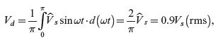 (5.33)
and
As another example, consider the load on the DC-side to have a large inductance, as shown in Figure 5.10a, such that the DC-side current is essentially DC. Assuming that ![]() to be purely DC, the waveforms are as shown in Figure 5.10b.
to be purely DC, the waveforms are as shown in Figure 5.10b.
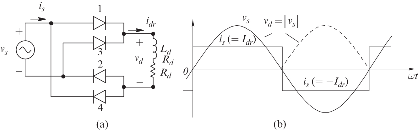
FIGURE 5.10 Full-bridge diode rectifier with an inductive load where  (DC).
(DC).
Note that the waveform of ![]() in Figure 5.10b is identical to that in Figure 5.9b for a resistive load. Therefore, the average value
in Figure 5.10b is identical to that in Figure 5.9b for a resistive load. Therefore, the average value ![]() of the voltage across the DC-side of the converter in Figure 5.10a is the same as in Equation (5.33), that is
of the voltage across the DC-side of the converter in Figure 5.10a is the same as in Equation (5.33), that is ![]() . Similarly, the average value of the DC-side current is related to
. Similarly, the average value of the DC-side current is related to ![]() by
by ![]() , as
, as ![]() .
.
5.4.1.1 DC-Bus Capacitor to Achieve a Low-Ripple in the DC-Side Voltage
Figures 5.9b and 5.10b show that the DC-side voltage has a large ripple. To eliminate this, in order to achieve a voltage waveform that is fairly DC, a large filter capacitor is connected on the DC-side, as shown in Figure 5.8a. As shown in Figure 5.11, at the beginning of the positive half-cycle of the input voltage ![]() , the capacitor is already charged to a DC voltage
, the capacitor is already charged to a DC voltage ![]() . So long as
. So long as ![]() exceeds the input voltage magnitude, all diodes remain reverse biased, and the input current is zero. Power to the equivalent resistance
exceeds the input voltage magnitude, all diodes remain reverse biased, and the input current is zero. Power to the equivalent resistance ![]() is supplied by the energy stored in the capacitor up to
is supplied by the energy stored in the capacitor up to ![]() .
.

FIGURE 5.11 Waveforms for the full-bridge diode rectifier with a DC-bus capacitor.
Beyond ![]() , the input current
, the input current ![]() increases, flowing through diodes
increases, flowing through diodes ![]() and
and ![]() . Beyond
. Beyond ![]() , the input voltage becomes smaller than the capacitor voltage, and the input current begins to decline, falling to zero at
, the input voltage becomes smaller than the capacitor voltage, and the input current begins to decline, falling to zero at ![]() . Beyond
. Beyond ![]() , until one half-cycle later than
, until one half-cycle later than ![]() , the input current remains zero, and the power to
, the input current remains zero, and the power to ![]() is supplied by the energy stored in the capacitor. At
is supplied by the energy stored in the capacitor. At ![]() during the negative half-cycle of the input voltage, the input current flows through diodes
during the negative half-cycle of the input voltage, the input current flows through diodes ![]() and
and ![]() . The rectifier DC-side current
. The rectifier DC-side current ![]() continues to flow in the same direction as during the positive half-cycle; however, the input current
continues to flow in the same direction as during the positive half-cycle; however, the input current ![]() , as shown in Figure 5.11. Figure 5.12 shows waveforms obtained by LTspice simulations for two values of the AC-side inductance, with current THD of 86% and 62%, respectively (higher inductance reduces THD, as discussed in the next section).
, as shown in Figure 5.11. Figure 5.12 shows waveforms obtained by LTspice simulations for two values of the AC-side inductance, with current THD of 86% and 62%, respectively (higher inductance reduces THD, as discussed in the next section).

FIGURE 5.12 Single-phase diode-bridge rectification for two values of Ls.
The fact that ![]() flows in the same direction during both the positive and the negative half-cycles represents the rectification process. In the circuit of Figure 5.8a in steady state, all waveforms repeat from one cycle to the next. Therefore, the average value of the capacitor current over a line-frequency cycle must be zero so that the DC-bus voltage is in steady state. As a consequence, the average current through the equivalent load-resistance
flows in the same direction during both the positive and the negative half-cycles represents the rectification process. In the circuit of Figure 5.8a in steady state, all waveforms repeat from one cycle to the next. Therefore, the average value of the capacitor current over a line-frequency cycle must be zero so that the DC-bus voltage is in steady state. As a consequence, the average current through the equivalent load-resistance ![]() equals the average of the rectifier DC-side current; that is,
equals the average of the rectifier DC-side current; that is, ![]() .
.
5.4.1.2 Effects of Ls and Cd on the Waveforms and the THD
As Figures 5.11 and 5.12 show, power is drawn from the utility supply by means of a pulse of current every half-cycle. The larger the “base” of this pulse during which the current flows, the lower its peak value and the total harmonic distortion (THD). This pulse widening can be accomplished by increasing the AC-side inductance ![]() . Another parameter under the designer’s control is the value of the DC-bus capacitor
. Another parameter under the designer’s control is the value of the DC-bus capacitor ![]() . At its minimum, it should be able to carry the ripple current in
. At its minimum, it should be able to carry the ripple current in ![]() and in
and in ![]() (which in practice is the input DC-side current, with a pulsating waveform, of a switch-mode converter) and keep the peak-to-peak ripple in the DC-bus voltage to some acceptable value, for example, less than 5% of the DC-bus average value. Assuming that these constraints are met, the lower the value of
(which in practice is the input DC-side current, with a pulsating waveform, of a switch-mode converter) and keep the peak-to-peak ripple in the DC-bus voltage to some acceptable value, for example, less than 5% of the DC-bus average value. Assuming that these constraints are met, the lower the value of ![]() , the lower the THD in current and the higher the ripple in the DC-bus voltage.
, the lower the THD in current and the higher the ripple in the DC-bus voltage.
In practice, it is almost impossible to meet the harmonic limits specified by IEEE-519 by using the above techniques. Rather, the power-factor-correction circuits described in the next chapter are needed to meet the harmonic specifications.
5.4.1.3 Simulation Using LTspice
The simulation of a single-phase diode-bridge rectifier is demonstrated by means of an example:
Example 5.2
In the single-phase diode-bridge rectifier shown in Figure 5.8a, ![]() ,
, ![]() ,
, ![]() , and
, and ![]() . The supply voltage is
. The supply voltage is ![]() RMS at
RMS at ![]() Simulate this rectifier using LTspice.
Simulate this rectifier using LTspice.
Solution The simulation file used in this example is available on the accompanying website. The LTspice model is shown in Figure 5.13, and the steady-state waveforms from the simulation of this model are shown in Figure 5.14.

FIGURE 5.13 LTspice model.

FIGURE 5.14 LTspice simulation results.
5.4.2 Three-Phase Diode-Rectifier Bridge
It is preferable to use a three-phase utility source, except at a fractional kilowatt, if such a supply is available. A commonly used full-bridge rectifier circuit is shown in Figure 5.15a.

FIGURE 5.15 Three-phase diode bridge rectifier.
To understand the circuit operation, the rectifier circuit can be drawn as in Figure 5.15b. The circuit consists of a top group and a bottom group of diodes. Initially, ![]() is ignored, and the DC-side current is assumed to flow continuously. At least one diode from each group must conduct to facilitate the flow of
is ignored, and the DC-side current is assumed to flow continuously. At least one diode from each group must conduct to facilitate the flow of ![]() . In the top group, all diodes have their cathodes connected together. Therefore, the diode connected to the most positive voltage will conduct; the other two will be reverse biased. In the bottom group, all diodes have their anodes connected together. Therefore, the diode connected to the most negative voltage will conduct; the other two will be reverse biased.
. In the top group, all diodes have their cathodes connected together. Therefore, the diode connected to the most positive voltage will conduct; the other two will be reverse biased. In the bottom group, all diodes have their anodes connected together. Therefore, the diode connected to the most negative voltage will conduct; the other two will be reverse biased.
Ignoring ![]() and assuming that the DC-side current
and assuming that the DC-side current ![]() is a pure DC, the waveforms are as shown in Figure 5.16. In Figure 5.16a, the waveforms (identified by the dark portions of the curves) show that each diode, based on the principle described above, conducts during
is a pure DC, the waveforms are as shown in Figure 5.16. In Figure 5.16a, the waveforms (identified by the dark portions of the curves) show that each diode, based on the principle described above, conducts during ![]() . The diodes are numbered so that they begin conducting sequentially: 1, 2, 3, and so on. The waveforms for the voltages
. The diodes are numbered so that they begin conducting sequentially: 1, 2, 3, and so on. The waveforms for the voltages ![]() and
and ![]() , with respect to the source-neutral, consist of
, with respect to the source-neutral, consist of ![]() -segments of the phase voltages, as shown in Figure 5.16a. The waveform of the DC-side voltage
-segments of the phase voltages, as shown in Figure 5.16a. The waveform of the DC-side voltage ![]() is shown in Figure 5.16b. It consists of
is shown in Figure 5.16b. It consists of ![]() -segments of the line-line voltages supplied by the utility. Line currents on the AC-side are as shown in Figure 5.16c. For example, phase-a current flows for
-segments of the line-line voltages supplied by the utility. Line currents on the AC-side are as shown in Figure 5.16c. For example, phase-a current flows for ![]() during each half-cycle of the phase-a input voltage; it flows through diode
during each half-cycle of the phase-a input voltage; it flows through diode ![]() during the positive half-cycle of
during the positive half-cycle of ![]() and through diode
and through diode ![]() during the negative half-cycle.
during the negative half-cycle.

FIGURE 5.16 Waveforms in a three-phase rectifier (a constant  ).
).
The average value of the DC-side voltage can be obtained by considering only a ![]() -segment in the 6-pulse (per line-frequency cycle) waveform shown in Figure 5.16b. Let us consider the instant of the peak in the
-segment in the 6-pulse (per line-frequency cycle) waveform shown in Figure 5.16b. Let us consider the instant of the peak in the ![]() -segment to be the time-origin, with
-segment to be the time-origin, with ![]() as the peak line-line voltage. The average value
as the peak line-line voltage. The average value ![]() can be obtained by calculating the integral from
can be obtained by calculating the integral from ![]() to
to ![]() (the area shown by the hatched area in Figure 5.16b) and then dividing by the interval
(the area shown by the hatched area in Figure 5.16b) and then dividing by the interval ![]() :
:
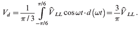 (5.35)
This average value is plotted as a straight line in Figure 5.16b.
5.4.2.1 Effect of DC-Bus Capacitor
In the three-phase rectifier of Figure 5.15a with the DC-bus capacitor filter, the input current waveforms obtained by computer simulations are shown in Figure 5.17.

FIGURE 5.17 Effect of  variation (a)
  ; (b)
; (b)  .
.
Figure 5.17a shows that the input current waveform within each half-cycle consists of two distinct pulses when ![]() is small. For example, in the
is small. For example, in the ![]() waveform during the positive half-cycle, the first pulse corresponds to the flow of DC-side current through the diode pair
waveform during the positive half-cycle, the first pulse corresponds to the flow of DC-side current through the diode pair ![]() and then through the diode pair
and then through the diode pair ![]() . At larger values of
. At larger values of ![]() , within each half-cycle, the input current between the two pulses does not go to zero, as shown in Figure 5.17b.
, within each half-cycle, the input current between the two pulses does not go to zero, as shown in Figure 5.17b.
The effects of ![]() and
and ![]() on the waveforms can be determined by a parametric analysis, similar to the case of single-phase rectifiers. The THD in the current waveform of Figure 5.17b is much smaller than in Figure 5.17a (23% versus 82%). The AC-side inductance
on the waveforms can be determined by a parametric analysis, similar to the case of single-phase rectifiers. The THD in the current waveform of Figure 5.17b is much smaller than in Figure 5.17a (23% versus 82%). The AC-side inductance ![]() is required to provide a line-frequency reactance
is required to provide a line-frequency reactance ![]() that is typically greater than 2% of the base impedance
that is typically greater than 2% of the base impedance ![]() , which is defined as follows:
, which is defined as follows:
where ![]() is the three-phase power rating of the power electronic system, and
is the three-phase power rating of the power electronic system, and ![]() is the RMS value of the phase voltage. Therefore, typically, the minimum AC-side inductance should be such that
is the RMS value of the phase voltage. Therefore, typically, the minimum AC-side inductance should be such that
5.4.2.2 Simulation Using LTspice
The simulation of a three-phase diode-bridge rectifier is demonstrated by means of an example:
Example 5.3
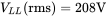
In the three-phase diode-bridge rectifier shown in Figure 5.15a, ![]() ,
, ![]() , and
, and ![]() . The supply voltage is
. The supply voltage is ![]() line-line RMS at
line-line RMS at ![]() . Simulate this rectifier using LTspice.
. Simulate this rectifier using LTspice.
Solution The simulation file used in this example is available on the accompanying website. The LTspice model is shown in Figure 5.18, and the steady-state waveforms from the simulation of this model are shown in Figure 5.19.

FIGURE 5.18 LTspice model.

FIGURE 5.19 LTspice simulation results.
5.4.3 Comparison of Single-Phase and Three-Phase Rectifiers
Examination of single-phase and three-phase rectifier waveforms shows the differences in their characteristics. Three-phase rectification results in six identical “pulses” per cycle in the rectified DC-side voltage, whereas single-phase rectification results in two such pulses. Therefore, three-phase rectifiers are superior in terms of minimizing distortion in line currents and ripple across the DC-bus voltage. Consequently, as stated earlier, three-phase rectifiers should be used if a three-phase supply is available. However, three-phase rectifiers, just like single-phase rectifiers, are also unable to meet the harmonic limits specified by IEEE-519 unless corrective actions such as those described in Chapter 12 are taken.
5.5 MEANS TO AVOID TRANSIENT INRUSH CURRENTS AT STARTING
In power electronic systems with rectifier front-ends, it may be necessary to take steps to avoid a large inrush of current at the instant the system is connected to the utility source. In such power electronic systems, the DC-bus capacitor is very large and initially has no voltage across it. Therefore, at the instant the switch in Figure 5.20a is closed to connect the power electronic system to the utility source, a large current flows through the diode-bridge rectifier, charging the DC-bus capacitor.

FIGURE 5.20 Means to avoid inrush current.
This transient current inrush is highly undesirable; fortunately, several means of avoiding it are available. These include using a front-end that consists of thyristors, discussed in Chapter 14, or using a series semiconductor switch as shown in Figure 5.16b. At the instant of starting, the resistance across the switch lets the DC-bus capacitor to get charged without a large inrush current, and subsequently, the semiconductor switch is turned on to bypass the resistance. There are other techniques that can also be employed.
5.6 FRONT-ENDS WITH BI-DIRECTIONAL POWER FLOW
In stop-and-go applications such as elevators, it is cost effective to feed the energy recovered by regenerative braking of the motor drive back into the utility supply. Converter arrangements for such applications are considered in Chapter 12.
REFERENCES
- 1. N. Mohan, T.M. Undeland, and W.P. Robbins, Power Electronics: Converters, Applications and Design, 3rd Edition (New York: John Wiley & Sons, 2003).
PROBLEMS
- 5.1 In a single-phase diode rectifier bridge,
 ,
,  and
and  . Calculate
  ,
,  , and PF.
 - 5.2 In a single-phase diode bridge rectifier circuit, the following operating conditions are given:
 ,
,  ,
,  , and
, and  . Calculate the following:
  ,
,  ,
,  , and
, and  .
. - 5.3 In a single-phase rectifier the input current can be approximated by a triangular waveform every half cycle with a peak of
 and a base of
  . Calculate the RMS current through each diode.
 - 5.4 In the above problem, calculate the ripple component in the DC-side current that will flow through the DC-side capacitor.
- 5.5 In a three-phase rectifier, if the input currents are of rectangular waveforms, as shown in Figure 5.16c, with an amplitude of 12 A, calculate
 ,
,  ,
,  ,
,  and the power factor. Assume that
  , as associated with the current waveforms in Figure 5.14c.
 - 5.6 In the above problem, calculate the three-phase power through the rectifier bridge if
 .
.
Simulation Problems
- 5.7 In the single-phase rectifier in Figure 5.8a,
 and
and 
- Obtain the %THD in the input current for the three values of the input inductance 1 mH, 3 mH, and 5 mH. Comment on the input current waveform as a function of the AC-side inductance in part (a).
- Measure the average and the peak-to-peak ripple in the output voltage for the three values of the input-side inductance in part (a), and comment on the output voltage waveform as a function of the AC-side inductance.
- Keeping the input inductance value as
 , change the DC-side capacitance values to be
  ,
,  and
and  . Measure the peak-to-peak ripple in the output capacitor voltage for these three values of the output capacitance.
- 5.8 In the three-phase rectifier in Figure 5.15a,
 Req = 16.5 Ω.
- Obtain the %THD in the input current for the three values of the input inductance of 0.1 mH, 0.5 mH, and 1.0 mH.
- Comment on the input current waveform as a function of the AC-side inductance for values.
- Comment on the output voltage waveform as a function of the AC-side inductance. Measure the average and the peak-to-peak ripple in the output voltage for the three values of the input-side inductance.
- Measure the peak-to-peak ripple in the output capacitor current for the three values of the input-side inductance. What is the fundamental frequency of this current?