
4
DESIGNING FEEDBACK CONTROLLERS IN SWITCH-MODE DC POWER SUPPLIES
In most applications discussed in Chapter 1, power electronic converters are operated in a controlled manner. The need for doing so is evident in electric drives used in transportation to control speed and position. The same is also true in photovoltaic systems, where we should operate at their maximum power point to derive the maximum power. In wind turbines, the generator speed should be controlled to operate the turbine blades at the maximum value of the turbine coefficient of performance. In DC-DC converters, with or without electrical isolation, the output voltage needs to be regulated at a specified value with a narrow tolerance. In this chapter, the fundamental concepts for feedback control are illustrated by means of regulated DC-DC converters.
4.1 INTRODUCTION AND OBJECTIVES OF FEEDBACK CONTROL
As shown in Figure 4.1, almost all DC-DC converters operate with their output voltage regulated to equal their reference value within a specified tolerance band (for example, ![]() around its nominal value) in response to disturbances in the input voltage and the output load. This regulation is achieved by pulsed-width-modulating the duty ratio
around its nominal value) in response to disturbances in the input voltage and the output load. This regulation is achieved by pulsed-width-modulating the duty ratio ![]() of their switching power-pole. In this chapter, we will design the feedback controller to regulate the output voltages of DC-DC converters.
of their switching power-pole. In this chapter, we will design the feedback controller to regulate the output voltages of DC-DC converters.

FIGURE 4.1 Regulated DC power supply.
The feedback controller to regulate the output voltage must be designed with the following objectives in mind: zero steady-state error, fast response to changes in the input voltage and the output load, low overshoot, and low noise susceptibility. We should note that in designing feedback controllers, all transformer-isolated topologies discussed later in Chapter 8 can be replaced by their basic single-switch topologies from which they are derived. The feedback control is described using the voltage-mode control, which is later extended to include the current-mode control.
The steps in designing the feedback controller are described as follows:
- Linearize the system for small changes around the DC steady-state operating point (bias point). This requires dynamic averaging, discussed in the previous chapter.
- Design the feedback controller using linear control theory.
- Confirm and evaluate the system response by simulations for large disturbances.
4.2 REVIEW OF LINEAR CONTROL THEORY
A feedback control system is shown in Figure 4.2, where the output voltage is measured and compared with a reference value ![]() . The error
. The error ![]() between the two acts on the controller, which produces the control voltage
between the two acts on the controller, which produces the control voltage ![]() . This control voltage acts as the input to the pulse-width modulator to produce a switching signal
. This control voltage acts as the input to the pulse-width modulator to produce a switching signal ![]() for the power pole in the DC-DC converter. The average value of this switching signal is
for the power pole in the DC-DC converter. The average value of this switching signal is ![]() , as shown in Figure 4.2.
, as shown in Figure 4.2.
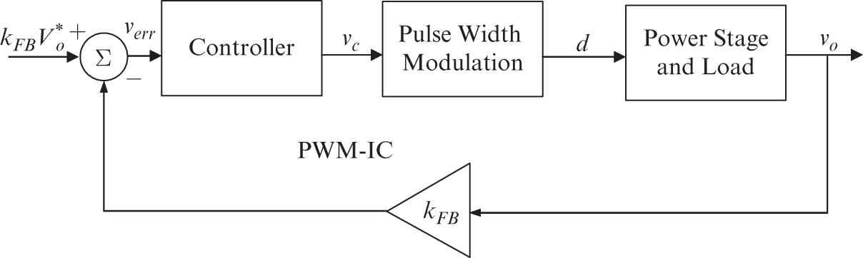
FIGURE 4.2 Feedback control.
To make use of linear control theory, various blocks in the power supply system of Figure 4.2 are linearized around the steady-state DC operating point, assuming small-signal perturbations. Each average quantity (represented by an overbar, i.e. a “−” on top) associated with the power pole of the converter topology can be expressed as the sum of its steady-state DC value (represented by an uppercase letter) and a small-signal perturbation (represented by a “~” on top), for example,
 (4.1)
(4.1)
where ![]() is already an averaged value and
is already an averaged value and ![]() does not contain any switching frequency component. Based on the small-signal perturbation quantities in the Laplace domain, the linearized system block diagram is as shown in Figure 4.3, where the perturbation in the reference input to this feedback-controlled system,
does not contain any switching frequency component. Based on the small-signal perturbation quantities in the Laplace domain, the linearized system block diagram is as shown in Figure 4.3, where the perturbation in the reference input to this feedback-controlled system, ![]() is zero since the output voltage is being regulated to its reference value. In Figure 4.3,
is zero since the output voltage is being regulated to its reference value. In Figure 4.3, ![]() is the transfer function of the pulse-width modulator and
is the transfer function of the pulse-width modulator and ![]() is the power stage transfer function. In the feedback path, the transfer function is of the voltage-sensing network, which can be represented by a simple gain
is the power stage transfer function. In the feedback path, the transfer function is of the voltage-sensing network, which can be represented by a simple gain ![]() , usually less than unity.
, usually less than unity. ![]() is the transfer function of the feedback controller that needs to be determined to satisfy the control objectives.
is the transfer function of the feedback controller that needs to be determined to satisfy the control objectives.

FIGURE 4.3 Small-signal control system representation.
As a review, the Bode plots of transfer functions with poles and zeros are discussed in Appendix 4A at the back of this chapter.
4.2.1 Loop Transfer Function 
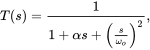
It is the closed-loop response (with the feedback in place) that we need to optimize. Using linear control theory, we can achieve this objective by ensuring certain characteristics of the loop transfer function ![]() . In the control block diagram of Figure 4.3, the loop transfer function (from point A to point B) is
. In the control block diagram of Figure 4.3, the loop transfer function (from point A to point B) is
4.2.2 Crossover Frequency  of
of 
In order to define a few necessary control terms, we will consider a generic Bode plot of the loop transfer function ![]() in terms of its magnitude and phase angle, shown in Figure 4.4 as a function of frequency. The frequency at which the gain equals unity (that is
in terms of its magnitude and phase angle, shown in Figure 4.4 as a function of frequency. The frequency at which the gain equals unity (that is ![]() ) is defined as the crossover frequency
) is defined as the crossover frequency ![]() (or
(or ![]() ). This crossover frequency is a good indicator of the bandwidth of the closed-loop feedback system, which determines the speed of the dynamic response of the control system to various disturbances.
). This crossover frequency is a good indicator of the bandwidth of the closed-loop feedback system, which determines the speed of the dynamic response of the control system to various disturbances.

FIGURE 4.4 Definitions of crossover frequency, gain margin, and phase margin.
4.2.3 Phase and Gain Margins
For the closed-loop feedback system to be stable, at the crossover frequency ![]() , the phase delay introduced by the loop transfer function must be less than
, the phase delay introduced by the loop transfer function must be less than ![]() . At
. At ![]() , the phase angle
, the phase angle ![]() of the loop transfer function
of the loop transfer function ![]() , measured with respect to
, measured with respect to ![]() , is defined as the phase margin (
, is defined as the phase margin (![]() ) as shown in Figure 4.4:
) as shown in Figure 4.4:
Note that ![]() is negative, but the phase margin in Equation (4.3) must be positive. Generally, feedback controllers are designed to yield a phase margin of approximately
is negative, but the phase margin in Equation (4.3) must be positive. Generally, feedback controllers are designed to yield a phase margin of approximately ![]() , since much smaller values result in high overshoots and long settling times (oscillatory response) and much larger values in a sluggish response.
, since much smaller values result in high overshoots and long settling times (oscillatory response) and much larger values in a sluggish response.
The gain margin is also defined in Figure 4.4, which shows that the gain margin is the value of the magnitude of the loop transfer function, measured below 0 dB, at the frequency at which the phase angle of the loop transfer function may (not always) cross ![]() . If the phase angle crosses
. If the phase angle crosses ![]() , the gain margin should generally be in excess of 10 dB in order to keep the system response from becoming oscillatory due to parameter changes and other variations.
, the gain margin should generally be in excess of 10 dB in order to keep the system response from becoming oscillatory due to parameter changes and other variations.
4.3 LINEARIZATION OF VARIOUS TRANSFER FUNCTION BLOCKS
To be able to apply linear control theory in the feedback controller design, it is necessary that all the blocks in Figure 4.2 be linearized around their DC steady-state operating point, as shown by transfer functions in Figure 4.3.
4.3.1 Linearizing the Pulse-Width Modulator
In the feedback control, a high-speed PWM integrated circuit such as the UC3824 [1] from Unitrode/Texas Instruments may be used. Functionally, within this PWM IC shown in Figure 4.5a, the control voltage ![]() generated by the error amplifier is compared with a ramp signal
generated by the error amplifier is compared with a ramp signal ![]() with a constant amplitude
with a constant amplitude ![]() at a constant switching frequency
at a constant switching frequency ![]() , as shown in Figure 4.5b. The output switching signal is represented by the switching function
, as shown in Figure 4.5b. The output switching signal is represented by the switching function ![]() , which equals 1 if
, which equals 1 if ![]() and is 0 otherwise. The switch duty ratio in Figure 4.5b is given as
and is 0 otherwise. The switch duty ratio in Figure 4.5b is given as

FIGURE 4.5 PWM waveforms.
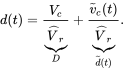
In terms of a disturbance around the DC steady-state operating point, the control voltage can be expressed as
Substituting Equation (4.5) into Equation (4.4),
 (4.6)
(4.6)
In Equation (4.6), the second term on the right side equals ![]() , from which the transfer function of the PWM IC is
, from which the transfer function of the PWM IC is
It is a constant gain transfer function, as shown in Figure 4.5c in the Laplace domain.
Example 4.1
In PWM ICs, there is usually a DC voltage offset in the ramp voltage, and instead of ![]() as shown in Figure 4.5b, a typical valley-to-peak value of the ramp signal is defined. In the PWM IC UC3824, this valley-to-peak value is 1.8 V. Calculate the linearized transfer function associated with this PWM-IC.
as shown in Figure 4.5b, a typical valley-to-peak value of the ramp signal is defined. In the PWM IC UC3824, this valley-to-peak value is 1.8 V. Calculate the linearized transfer function associated with this PWM-IC.
Solution The DC offset in the ramp signal does not change its small-signal transfer function. Hence, the peak-to-valley voltage can be treated as ![]() Using Equation (4.7),
Using Equation (4.7),
4.3.2 Linearizing the Power Stage of DC-DC Converters in CCM
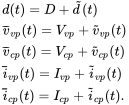
To design feedback controllers, the power stage of the converters must be linearized around the steady-state DC operating point, assuming a small-signal disturbance. Figure 4.6a shows the average model of the switching power-pole, where the subscript “vp” refers to the voltage port and “cp” to the current port. Each average quantity in Figure 4.6a can be expressed as the sum of its steady-state DC value (represented by an uppercase letter) and a small-signal perturbation (represented by a tilde “∼” on top):
 (4.9)
(4.9)

FIGURE 4.6 Linearizing the switching power-pole.
Utilizing the voltage and current relationships between the two ports in Figure 4.6a and expressing each variable as in Equation (4.9),
and
Equating the perturbation terms on both sides of the above equations,
The two equations above are linearized by neglecting the products of small-perturbation terms. The resulting linear equations are
and
Equations (4.12) and (4.13) can be represented by means of an ideal transformer shown in Figure 4.6b, which is a linear representation of the power pole for small signals around a steady-state operating point given by D, ![]() , and
, and ![]() .
.
The average representations of buck, boost, and buck-boost converters are shown in Figure 4.7a. Replacing the power pole in each of these converters by its small-signals linearized representation, the resulting circuits are shown in Figure 4.7b, where the perturbation ![]() is zero-based on the assumption of a constant DC input voltage
is zero-based on the assumption of a constant DC input voltage ![]() , and the output capacitor ESR is represented by
, and the output capacitor ESR is represented by ![]() Note that in boost converters, since the transistor is in the bottom position of the switching power-pole,
Note that in boost converters, since the transistor is in the bottom position of the switching power-pole, ![]() in Figure 4.6a needs to be replaced by
in Figure 4.6a needs to be replaced by ![]() . Substituting
. Substituting ![]() with
with ![]() results in
results in ![]() . Therefore,
. Therefore, ![]() in Equations (4.12) and (4.13) needs to be replaced by
in Equations (4.12) and (4.13) needs to be replaced by ![]() and
and ![]() by
by ![]() .
.

FIGURE 4.7 Linearizing single-switch converters in CCM.
As fully explained in Appendix 4B, all three circuits for small-signal perturbations in Figure 4.7b have the same form as shown in Figure 4.8. In this equivalent circuit, the effective inductance ![]() is the same as the actual inductance
is the same as the actual inductance ![]() in the buck converter, since in both states of a buck converter in CCM,
in the buck converter, since in both states of a buck converter in CCM, ![]() and
and ![]() are always connected together. However, in boost and buck-boost converters, these two elements are not always connected, resulting in
are always connected together. However, in boost and buck-boost converters, these two elements are not always connected, resulting in ![]() to be
to be ![]() in Figure 4.8:
in Figure 4.8:

FIGURE 4.8 Small-signal equivalent circuit for buck, boost, and buck-boost converters.
Transfer functions of the three converters in CCM from Appendix 4B are repeated below:
In the above power-stage transfer functions in CCM, there are several characteristics worth noting. There are two poles created by the low-pass L-C filter in Figure 4.8, and the capacitor ESR ![]() results in a zero. In boost and buck-boost converters, their transfer functions depend on the steady-state operating value
results in a zero. In boost and buck-boost converters, their transfer functions depend on the steady-state operating value ![]() . They also have a right-half-plane zero, whose presence can be explained by the fact that in these converters, increasing the duty ratio for increasing the output, for example, initially has an opposite consequence by isolating the input stage from the output load for a longer time.
. They also have a right-half-plane zero, whose presence can be explained by the fact that in these converters, increasing the duty ratio for increasing the output, for example, initially has an opposite consequence by isolating the input stage from the output load for a longer time.
4.3.2.1 Using Computer Simulation to Obtain 
Transfer functions given by Equations (4.15) through (4.17) provide theoretical insight into the converter operation. However, the Bode plots of the transfer function can be obtained with similar accuracy by means of linearization and AC analysis, using a computer program such as LTspice. The converter circuit is simulated as shown in Figure 4.9 in the example below for a frequency-domain AC analysis, using the switching power-pole average model discussed in Chapter 3 and shown in Figure 4.6a. The duty cycle perturbation ![]() is represented as an AC source whose frequency is swept over several decades of interest and whose amplitude is kept constant, for example, at 1 V. In such a simulation, LTspice first calculates voltages and currents at the DC steady-state operating point, linearizes the circuit around this DC bias point, and then performs the AC analysis.
is represented as an AC source whose frequency is swept over several decades of interest and whose amplitude is kept constant, for example, at 1 V. In such a simulation, LTspice first calculates voltages and currents at the DC steady-state operating point, linearizes the circuit around this DC bias point, and then performs the AC analysis.

FIGURE 4.9 LTspice circuit model for a buck converter.
Example 4.2
A buck converter has the following parameters and is operating in CCM:![]() ,
, ![]()
![]() ,
, ![]() ,
, ![]() , and
, and ![]() . The duty ratio
. The duty ratio ![]() is adjusted to regulate the output voltage
is adjusted to regulate the output voltage ![]() . Obtain the gain and the phase of the power stage
. Obtain the gain and the phase of the power stage ![]() for frequencies ranging from 1 Hz to 100 kHz.
for frequencies ranging from 1 Hz to 100 kHz.
Solution The LTspice circuit is shown in Figure 4.9 where the DC voltage source {D}, representing the duty ratio D, establishes the DC operating point. The duty ratio perturbation ![]() is represented as an AC source whose frequency is swept over several decades of interest, keeping the amplitude constant. (Since the circuit is linearized before the AC analysis, the best choice for the AC source amplitude is 1 V.) The switching power-pole is represented by an ideal transformer, which consists of two dependent sources: a dependent current source and a dependent voltage source. The circuit parameters are specified by means of parameter blocks within LTspice.
is represented as an AC source whose frequency is swept over several decades of interest, keeping the amplitude constant. (Since the circuit is linearized before the AC analysis, the best choice for the AC source amplitude is 1 V.) The switching power-pole is represented by an ideal transformer, which consists of two dependent sources: a dependent current source and a dependent voltage source. The circuit parameters are specified by means of parameter blocks within LTspice.
The Bode plot of the frequency response is shown in Figure 4.10. It shows that at the crossover frequency ![]() selected in the next example, Example 4.3, the power stage has
selected in the next example, Example 4.3, the power stage has ![]() and
and ![]() . We will make use of these values in Example 4.3.
. We will make use of these values in Example 4.3.

FIGURE 4.10 The gain and the phase of the power stage  .
.
4.4 FEEDBACK CONTROLLER DESIGN IN VOLTAGE-MODE CONTROL
The feedback controller design is presented by means of a numerical example to regulate the buck converter described earlier in Example 4.2. The controller is designed for the continuous conduction mode (CCM) at full load, which, although not optimum, is stable in DCM.
Example 4.3
Design the feedback controller for the buck converter described in Example 4.2. The PWM IC is as described in Example 4.1. The output voltage-sensing network in the feedback path has a gain ![]() . The steady-state error is required to be zero, and the phase margin of the loop transfer function should be
. The steady-state error is required to be zero, and the phase margin of the loop transfer function should be ![]() at as high a crossover frequency as possible.
at as high a crossover frequency as possible.
Solution In deciding on the transfer function ![]() of the controller, the control objectives translate into the following simultaneous characteristics of the loop transfer function
of the controller, the control objectives translate into the following simultaneous characteristics of the loop transfer function ![]() , from which
, from which ![]() can be designed:
can be designed:
- The crossover frequency
 of the loop gain is as high as possible to result in a fast response of the closed-loop system.
 - The phase angle of the loop transfer function has the specified phase margin, typically
 at the crossover frequency, so that the response in the closed-loop system settles quickly without oscillations.
 - The phase angle of the loop transfer function should not drop below
 at frequencies below the crossover frequency.
The Bode plot for the power stage is obtained earlier, as shown in Figure 4.10 of Example 4.2. In this Bode plot, the phase angle drops toward ![]() due to the two poles of the L-C filter shown in the equivalent circuit of Figure 4.8 and confirmed by the transfer function of Equation (4.15). Beyond the L-C filter resonance frequency, the phase angle increases toward
due to the two poles of the L-C filter shown in the equivalent circuit of Figure 4.8 and confirmed by the transfer function of Equation (4.15). Beyond the L-C filter resonance frequency, the phase angle increases toward ![]() because of the zero introduced by the output capacitor ESR in the transfer function of the power stage. We should not rely on this capacitor ESR, which is not accurately known and can have a large variability.
because of the zero introduced by the output capacitor ESR in the transfer function of the power stage. We should not rely on this capacitor ESR, which is not accurately known and can have a large variability.
A simple procedure based on the K-factor approach [2] is presented below, which lends itself to a straightforward step-by-step design. For the reasons given below, the transfer function ![]() of the controller is selected to be of the form in Equation (4.18), and its Bode plot is shown in Figure 4.11.
of the controller is selected to be of the form in Equation (4.18), and its Bode plot is shown in Figure 4.11.

FIGURE 4.11 Bode plot of GC (s) in Equation (4.18).
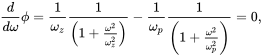
To yield a zero steady-state error, ![]() contains a pole at the origin, which introduces a
contains a pole at the origin, which introduces a ![]() phase shift in the loop transfer function. The phase of the transfer function peaks at the geometric mean
phase shift in the loop transfer function. The phase of the transfer function peaks at the geometric mean ![]() of the zero and pole frequencies, as shown in Figure 4.11, where
of the zero and pole frequencies, as shown in Figure 4.11, where ![]() and
and ![]() are chosen such that their geometric mean
are chosen such that their geometric mean ![]() is equal to the loop crossover frequency
is equal to the loop crossover frequency ![]() .
.
The crossover frequency ![]() of the loop is chosen beyond the L-C resonance frequency of the power stage, where, unfortunately,
of the loop is chosen beyond the L-C resonance frequency of the power stage, where, unfortunately, ![]() has a large negative value. The sum of
has a large negative value. The sum of ![]() (due to the pole at the origin in
(due to the pole at the origin in ![]() ) and
) and ![]() is more negative than
is more negative than ![]() . Therefore, to obtain a phase margin of
. Therefore, to obtain a phase margin of ![]() requires boosting the phase at
requires boosting the phase at ![]() , by more than
, by more than ![]() , by placing two coincident zeroes at
, by placing two coincident zeroes at ![]() to nullify the effect of the two poles in the power-stage transfer function
to nullify the effect of the two poles in the power-stage transfer function ![]() . Two coincident poles are placed at
. Two coincident poles are placed at ![]() (>
(>![]() ) to roll off the gain rapidly much before the switching frequency. The controller gain
) to roll off the gain rapidly much before the switching frequency. The controller gain ![]() is such that the loop gain equals unity at the crossover frequency.
is such that the loop gain equals unity at the crossover frequency.
The input specifications in determining the parameters of the controller transfer function in Equation (4.18) are ![]() ,
, ![]() as shown in Figure 4.11, and the controller gain
as shown in Figure 4.11, and the controller gain![]() . A step-by-step procedure for designing
. A step-by-step procedure for designing ![]() is described below.
is described below.
Step 1: Choose the crossover frequency. Choose ![]() to be slightly beyond the L-C resonance frequency
to be slightly beyond the L-C resonance frequency ![]() , which in this example is approximately
, which in this example is approximately ![]() Hz. Therefore, we will choose
Hz. Therefore, we will choose ![]() . This ensures that the phase angle of the loop remains greater than
. This ensures that the phase angle of the loop remains greater than ![]() at all frequencies below
at all frequencies below ![]() .
.
Step 2: Calculate the needed phase boost. The desired phase margin is specified as ![]() . The required phase boost
. The required phase boost ![]() at the crossover frequency is calculated as follows, noting that
at the crossover frequency is calculated as follows, noting that ![]() and
and ![]() produce zero phase shift:
produce zero phase shift:
Substituting Equations (4.20) and (4.21) into Equation (4.19),
In Figure 4.10, ![]() , substituting which in Equation (4.22), with
, substituting which in Equation (4.22), with![]() , yields the required phase boost
, yields the required phase boost![]() .
.
Step 3: Calculate the controller gain at the crossover frequency. From Equation (4.2) at the crossover frequency ![]() ,
,
In Figure 4.10, at ![]() ,
, ![]() . Therefore in Equation (4.23), using the gain of the PWM block calculated in Example 4.1,
. Therefore in Equation (4.23), using the gain of the PWM block calculated in Example 4.1,
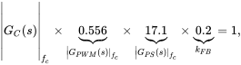 (4.24)
or
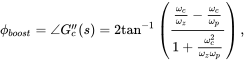
The controller in Equation (4.18) with two pole-zero pairs is analyzed in Appendix 4C. According to this analysis, the phase angle of ![]() in Equation (4.18) reaches its maximum at the geometric mean frequency
in Equation (4.18) reaches its maximum at the geometric mean frequency ![]() , where the phase boost
, where the phase boost ![]() , as shown in Figure 4.11, is measured with respect to
, as shown in Figure 4.11, is measured with respect to ![]() . By proper choice of the controller parameters, the geometric mean frequency is made equal to the crossover frequency
. By proper choice of the controller parameters, the geometric mean frequency is made equal to the crossover frequency ![]() . We introduce a factor
. We introduce a factor ![]() that indicates the geometric separation between poles and zeroes to yield the necessary phase boost:
that indicates the geometric separation between poles and zeroes to yield the necessary phase boost:
As shown in Appendix 4C, ![]() can be derived in terms of
can be derived in terms of ![]() as follows:
as follows:
Using the value of ![]() into Equation (4.26), and the fact that we will select
into Equation (4.26), and the fact that we will select ![]() to equal the chosen crossover frequency
to equal the chosen crossover frequency ![]() , the pole and the zero frequencies in the controller can be calculated as follows:
, the pole and the zero frequencies in the controller can be calculated as follows:
From Equations (4.26), (4.28), and (4.29), the controller gain ![]() in Equation (4.18) can be calculated at
in Equation (4.18) can be calculated at ![]() as
as
Once the parameters in Equation (4.18) are determined, the controller transfer function can be synthesized by a single op-amp circuit shown in Figure 4.12. The choice of ![]() in Figure 4.12 is based on how much current can be drawn from the sensor output; other resistances and capacitances are chosen using the relationships derived in Appendix 4C and presented below:
in Figure 4.12 is based on how much current can be drawn from the sensor output; other resistances and capacitances are chosen using the relationships derived in Appendix 4C and presented below:

FIGURE 4.12 Controller implementation of of−Gc(s), using Equation (4.18), by an op-amp.
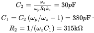
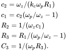
In this numerical example with ![]() ,
, ![]() , and
, and ![]() , we can calculate
, we can calculate ![]() in Equation (4.27). Using Equations (4.28) through (4.30),
in Equation (4.27). Using Equations (4.28) through (4.30), ![]() ,
, ![]() , and
, and ![]() . For the op-amp implementation, we will select
. For the op-amp implementation, we will select ![]() . From Equation (4.31),
. From Equation (4.31), ![]() ,
, ![]() ,
, ![]() ,
, ![]() , and
, and ![]() .
.
4.4.1 Simulation and Hardware Prototyping
The simulation of a voltage-mode control of buck converter using both LTspice and Workbench is demonstrated by means of an example:
Example 4.4
A buck converter is operating in CCM and has the following parameters: ![]()
![]() , ESR
, ESR ![]() , and load resistance
, and load resistance ![]() . It is operating in DC steady state under the following conditions:
. It is operating in DC steady state under the following conditions: ![]() ,
, ![]() , and
, and ![]() . For the switch and the diode, use the parameters given in the Appendix of Chapter 2. Design a voltage-mode controller to keep the voltage around this operating condition under varying input voltage and load. Assume that in the voltage feedback network,
. For the switch and the diode, use the parameters given in the Appendix of Chapter 2. Design a voltage-mode controller to keep the voltage around this operating condition under varying input voltage and load. Assume that in the voltage feedback network, ![]() . Simulate this converter using LTspice.
. Simulate this converter using LTspice.
Solution The simulation file used in this example is available on the accompanying website. The controller parameters are computed using Workbench script in which Equation (4.19) through Equation (4.30) has been implemented as shown in Figure 4.13. Using a script file to auto-generate parameters helps quickly iterate through multiple design choices.

FIGURE 4.13 Workbench script for computation of controller parameters.
The crossover frequency is chosen at twice the ![]() resonance frequency, which comes out to be
resonance frequency, which comes out to be ![]() . The phase margin is chosen to be
. The phase margin is chosen to be ![]() . The controller parameters computed by the script file are:
. The controller parameters computed by the script file are: ![]() ,
, ![]() , and
, and ![]() .
.
Using the above parameters, the controller is implemented by an op-amp in LTspice, as shown in Figure 4.14. The waveforms from the simulation of this model for a step-change in the load at ![]() is shown in Figure 4.15.
is shown in Figure 4.15.
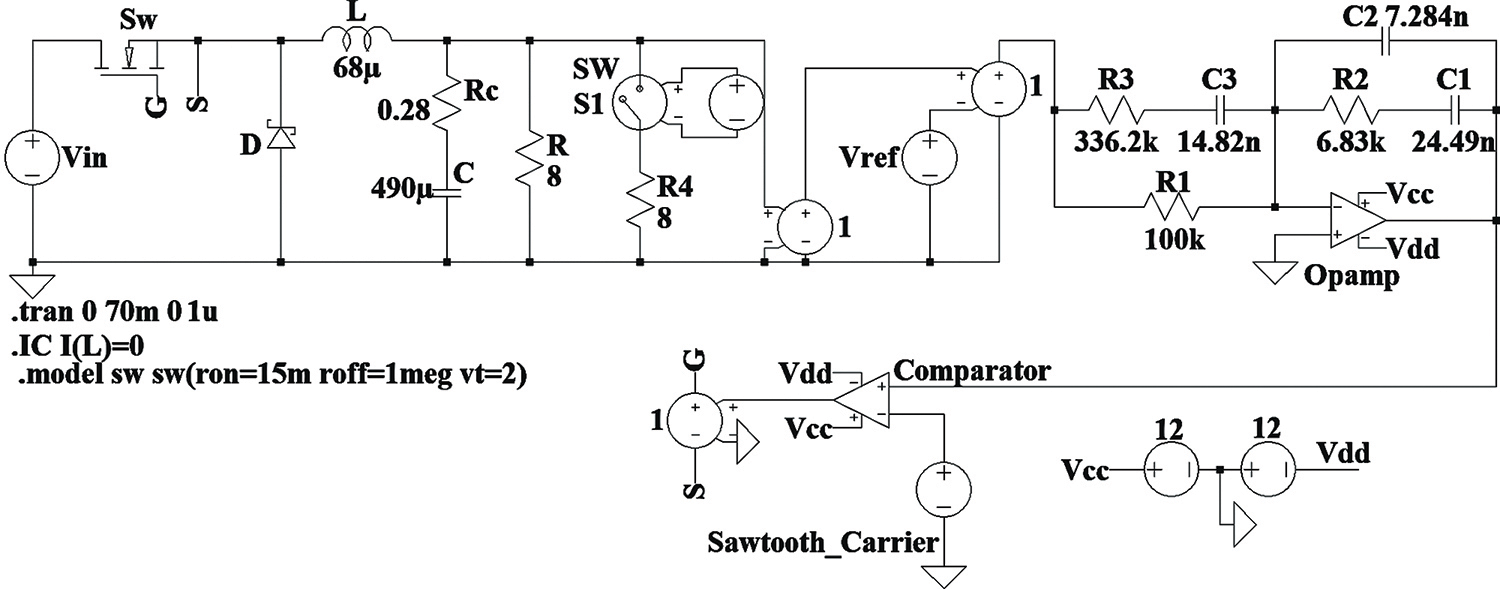
FIGURE 4.14 LTspice model.

FIGURE 4.15 LTspice simulation results.
The same model can be implemented using Workbench, as shown in Figure 4.16. The advantage of using Workbench is that the controller can be implemented in the transfer function form as given by Equation (4.18) without having to convert it to an equivalent op-amp-based circuit. The implementation within the controller subsystem in Figure 4.16 is shown in Figure 4.17.
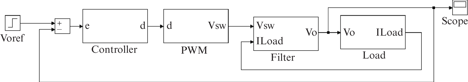
FIGURE 4.16 Workbench model.

FIGURE 4.17 Controller subsystem.
In the model, the output reference voltage is stepped from an initial value of ![]() to
to ![]() at time
at time ![]() . The load is doubled, i.e. the load resistance is halved from
. The load is doubled, i.e. the load resistance is halved from ![]() to
to ![]() at
at ![]() . Finally, at
. Finally, at ![]() the input voltage is stepped up to
the input voltage is stepped up to ![]() from the previous value of
from the previous value of ![]() . Through this, the output voltage is maintained at
. Through this, the output voltage is maintained at ![]() by the controller as shown in Figure 4.18.
by the controller as shown in Figure 4.18.

FIGURE 4.18 Output voltage waveform.
The Workbench model for implementing the above example in hardware using the Sciamble lab kit is shown in Figure 4.19. As mentioned earlier, the controller can be implemented directly in transfer function form, as shown in Figure 4.19. Unlike the op-amp-based controller implementation, where any changes to parameters would require changing physical components, the digital implementation shown here is merely a matter of changing the numerical values in the software. This allows for rapid prototyping of various controllers using the same hardware.

FIGURE 4.19 Workbench model.
The steady-state waveforms from running the buck converter using the Sciamble laboratory kit are shown in Figure 4.20. The converter output voltage settles down to the desired reference voltage as seen in Figure 4.20a and remains at the reference voltage for changing load resistance as seen in Figure 4.20b. Figure 4.20c shows the zoomed-in version of the waveforms over a few switching cycles. The step-by-step procedure for recreating the above hardware implementation is presented in [3].


FIGURE 4.20 Workbench hardware results: (a) step change in reference voltage, (b) gradual change in load resistance, and (c) switching cycle waveforms. (1) input current, (2) switch-node voltage, (3) inductor current, and (4) output voltage. For clarity, see the waveforms in color in the Appendix on the accompanying website.
4.5 PEAK-CURRENT MODE CONTROL
Current-mode control is often used in practice due to its many desirable features, such as simpler controller design and inherent current limiting. In such a control scheme, an inner control loop inside the outer voltage loop is used, as shown in Figure 4.21, resulting in a peak-current-mode control system. In this control arrangement, another state variable, the inductor current, is utilized as a feedback signal.

FIGURE 4.21 Peak current mode control.
The overall voltage-loop objectives in the current-mode control are the same as in the voltage-mode control discussed earlier. However, the voltage-loop controller here produces the reference value for the current that should flow through the inductor, hence the name current-mode control. There are two types of current-mode control:
- Peak-current-mode control
- Average-current-mode control.
In switch-mode DC power supplies, peak-current-mode control is invariably used, and therefore we will concentrate on it here. (We will examine the average-current-mode control in connection with the power-factor-correction circuits discussed in the next chapter.)
For the current loop, the outer voltage loop in Figure 4.21 produces the reference value ![]() of the inductor current. This reference current signal is compared with the measured inductor current
of the inductor current. This reference current signal is compared with the measured inductor current ![]() to reset the flip-flop when
to reset the flip-flop when ![]() reaches
reaches ![]() . As shown in Figures 4.21 and 4.22a, in generating
. As shown in Figures 4.21 and 4.22a, in generating ![]() , the voltage controller output
, the voltage controller output ![]() is modified by a signal called the slope compensation, which is necessary to avoid oscillations at the sub-harmonic frequencies of
is modified by a signal called the slope compensation, which is necessary to avoid oscillations at the sub-harmonic frequencies of ![]() , particularly at the duty ratio
, particularly at the duty ratio ![]() . Generally, the slope of this compensation signal is less than one-half of the slope at which the inductor current falls when the transistor in the converter is turned off.
. Generally, the slope of this compensation signal is less than one-half of the slope at which the inductor current falls when the transistor in the converter is turned off.

FIGURE 4.22 Peak-current-mode control with slope compensation.
In Figure 4.22a, when the inductor current reaches the reference value, the transistor is turned off and is turned back on at a regular interval ![]() set by the clock. For small perturbations, this current loop acts extremely fast, and it can be assumed ideal with a gain of unity in the small-signal block diagram of Figure 4.22b. The design of the outer voltage loop is described by means of the example below of a buck-boost converter operating in CCM.
set by the clock. For small perturbations, this current loop acts extremely fast, and it can be assumed ideal with a gain of unity in the small-signal block diagram of Figure 4.22b. The design of the outer voltage loop is described by means of the example below of a buck-boost converter operating in CCM.
Example 4.5
In this example, we will design a peak-current-mode controller for a buck-boost converter [4] that has the following parameters and operating conditions: ![]() ,
, ![]() ,
, ![]() ,
, ![]() ,
, ![]() . The output power
. The output power ![]() in CCM and the duty ratio
in CCM and the duty ratio ![]() is adjusted to regulate the output voltage
is adjusted to regulate the output voltage ![]() . The phase margin required for the voltage loop is
. The phase margin required for the voltage loop is ![]() . Assume that in the voltage feedback network,
. Assume that in the voltage feedback network, ![]() .
.
Solution In designing the outer voltage loop in Figure 4.22b, the transfer function needed for the power stage is ![]() . This transfer function in CCM can be obtained theoretically. However, it is much easier to obtain the Bode plot of this transfer function by means of a computer simulation, similar to that used for obtaining the Bode plots of
. This transfer function in CCM can be obtained theoretically. However, it is much easier to obtain the Bode plot of this transfer function by means of a computer simulation, similar to that used for obtaining the Bode plots of ![]() in Example 4.3 for a buck converter. The LTspice simulation diagram is shown in Figure 4.23 for the buck-boost converter, where, as discussed earlier, an ideal transformer is used for the average representation of the switching power-pole in CCM.
in Example 4.3 for a buck converter. The LTspice simulation diagram is shown in Figure 4.23 for the buck-boost converter, where, as discussed earlier, an ideal transformer is used for the average representation of the switching power-pole in CCM.

FIGURE 4.23 LTspice circuit for the buck-boost converter.
In Figure 4.23, the DC voltage source represents the switch duty ratio ![]() and establishes the DC steady state, around which the circuit is linearized. In the AC analysis, the frequency of the AC source, which represents the duty-ratio perturbation
and establishes the DC steady state, around which the circuit is linearized. In the AC analysis, the frequency of the AC source, which represents the duty-ratio perturbation ![]() , is swept over the desired range, and the ratio of
, is swept over the desired range, and the ratio of ![]() and
and ![]() yields the Bode plot of the power stage
yields the Bode plot of the power stage ![]() , as shown in Figure 4.24.
, as shown in Figure 4.24.

FIGURE 4.24 Bode plot of 
As shown in Figure 4.24, the phase angle of the power-stage transfer function levels off at approximately ![]() at ≃
at ≃ ![]() . The crossover frequency is chosen to be
. The crossover frequency is chosen to be ![]() , at which in Figure 4.24,
, at which in Figure 4.24, ![]() The power-stage transfer function
The power-stage transfer function ![]() of buck-boost converters contains a right-half-plane zero in CCM, and the crossover frequency is chosen well below the frequency of the right-half-plane zero. To achieve the desired phase margin of
of buck-boost converters contains a right-half-plane zero in CCM, and the crossover frequency is chosen well below the frequency of the right-half-plane zero. To achieve the desired phase margin of ![]() , the controller transfer function is chosen as expressed below:
, the controller transfer function is chosen as expressed below:
To yield zero steady-state error, it contains a pole at the origin that introduces a ![]() phase angle. The phase-boost required from this pole-zero combination in Equation (4.32), using Equation (4.22) and
phase angle. The phase-boost required from this pole-zero combination in Equation (4.32), using Equation (4.22) and ![]() , is
, is ![]() . Therefore, unlike the controller transfer function of Equation (4.18) for the voltage-mode control, only a single pole-zero pair is needed to provide a phase boost. In Equation (4.32), the zero and pole frequencies associated with the required phase boost can be derived, as shown in Appendix 4C, where
. Therefore, unlike the controller transfer function of Equation (4.18) for the voltage-mode control, only a single pole-zero pair is needed to provide a phase boost. In Equation (4.32), the zero and pole frequencies associated with the required phase boost can be derived, as shown in Appendix 4C, where ![]() is the same as in Equation (4.26), that is,
is the same as in Equation (4.26), that is, ![]() :
:
At the crossover frequency, as shown in Figure 4.24, the power stage transfer function has a gain ![]() Therefore, at the crossover frequency, by definition, in Figure 4.22b,,
Therefore, at the crossover frequency, by definition, in Figure 4.22b,,
Hence,
Using the equations above for ![]()
![]() and
and ![]()
![]() in Equation (4.33). Therefore, the parameters in the controller transfer function of Equation (4.32) are calculated as
in Equation (4.33). Therefore, the parameters in the controller transfer function of Equation (4.32) are calculated as ![]()
![]() and
and ![]()
The transfer function of Equation (4.32) can be realized by an op-amp circuit shown in Figure 4.25. In the expressions derived in Appendix 4C, selecting ![]() and using the transfer-function parameters calculated above, the component values in the circuit of Figure 4.25 are as follows:
and using the transfer-function parameters calculated above, the component values in the circuit of Figure 4.25 are as follows:
 (4.39)

FIGURE 4.25 Controller implementation of  using Equation (4.32), by an op-amp.
4.5.1 Simulation and Hardware Prototyping
Example 4.6
A buck-boost converter is operating in CCM and has the following parameters: ![]() ,
, ![]() , ESR
, ESR ![]() , and load resistance
, and load resistance ![]() . It is operating in DC steady state under the following conditions:
. It is operating in DC steady state under the following conditions: ![]() ,
, ![]() , and
, and ![]() . For the switch and the diode, use the parameters given in the Appendix of Chapter 2. Design a peak-current-mode controller to keep the voltage around this operating condition under varying input voltage and load. Assume that in the voltage feedback network,
. For the switch and the diode, use the parameters given in the Appendix of Chapter 2. Design a peak-current-mode controller to keep the voltage around this operating condition under varying input voltage and load. Assume that in the voltage feedback network, ![]() . Simulate this converter using LTspice.
. Simulate this converter using LTspice.
Solution The simulation file used in this example is available on the accompanying website. The controller parameters are computed using Workbench script in which Equation (4.32) through Equation (4.38) has been implemented.
The crossover frequency is chosen to be ![]() , below the frequency of the ESR zero, which occurs at
, below the frequency of the ESR zero, which occurs at ![]() , to continue the gain roll-off at higher frequencies. The phase margin is chosen to be
, to continue the gain roll-off at higher frequencies. The phase margin is chosen to be ![]() . The controller parameters computed by the script file are:
. The controller parameters computed by the script file are: ![]() ,
, ![]() , and
, and ![]() .
.
Using the above parameters, the controller is implemented by an op-amp in LTspice, as shown in Figure 4.26. The waveforms from the simulation of this model for a step-change in the load at ![]() is shown in Figure 4.27.
is shown in Figure 4.27.

FIGURE 4.26 LTspice model.

FIGURE 4.27 LTspice simulation results.
The same model can be implemented using Workbench, as shown in Figure 4.28. The voltage controller can be implemented in transfer function form, as given by Equation (4.32), as shown in Figure 4.29a, and the current controller as shown in Figure 4.29b.

FIGURE 4.28 Workbench model.
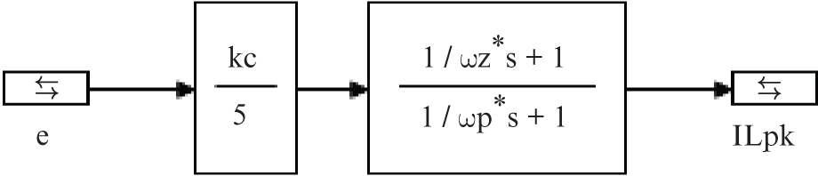
FIGURE 4.29A Controller subsystem.

FIGURE 4.29B Controller subsystem.
In the model, the output reference voltage is stepped from an initial value of ![]() to
to ![]() at time
at time ![]() . The load is doubled, i.e. the load resistance is halved from
. The load is doubled, i.e. the load resistance is halved from ![]() to
to ![]() at
at ![]() . Finally, at
. Finally, at ![]() the input voltage is stepped up to
the input voltage is stepped up to ![]() from the previous value of
from the previous value of ![]() . Through this, the output voltage is maintained at
. Through this, the output voltage is maintained at ![]() by the controller as shown in Figure 4.30.
by the controller as shown in Figure 4.30.

FIGURE 4.30 Output voltage waveform.
The Workbench model for implementing the above example in hardware using the Sciamble lab kit is shown in Figure 4.19. As mentioned earlier, the controller can be implemented directly in transfer function form, as shown in Figure 4.31.

FIGURE 4.31 Workbench model.
The steady-state waveforms from running the buck converter using the Sciamble laboratory kit are shown in Figure 4.32. The converter output voltage settles down to the desired reference voltage as seen in Figure 4.32a. Figure 4.32b shows the zoomed-in version of the waveforms over a few switching cycles. The step-by-step procedure for re-creating the above hardware implementation is presented in [4].
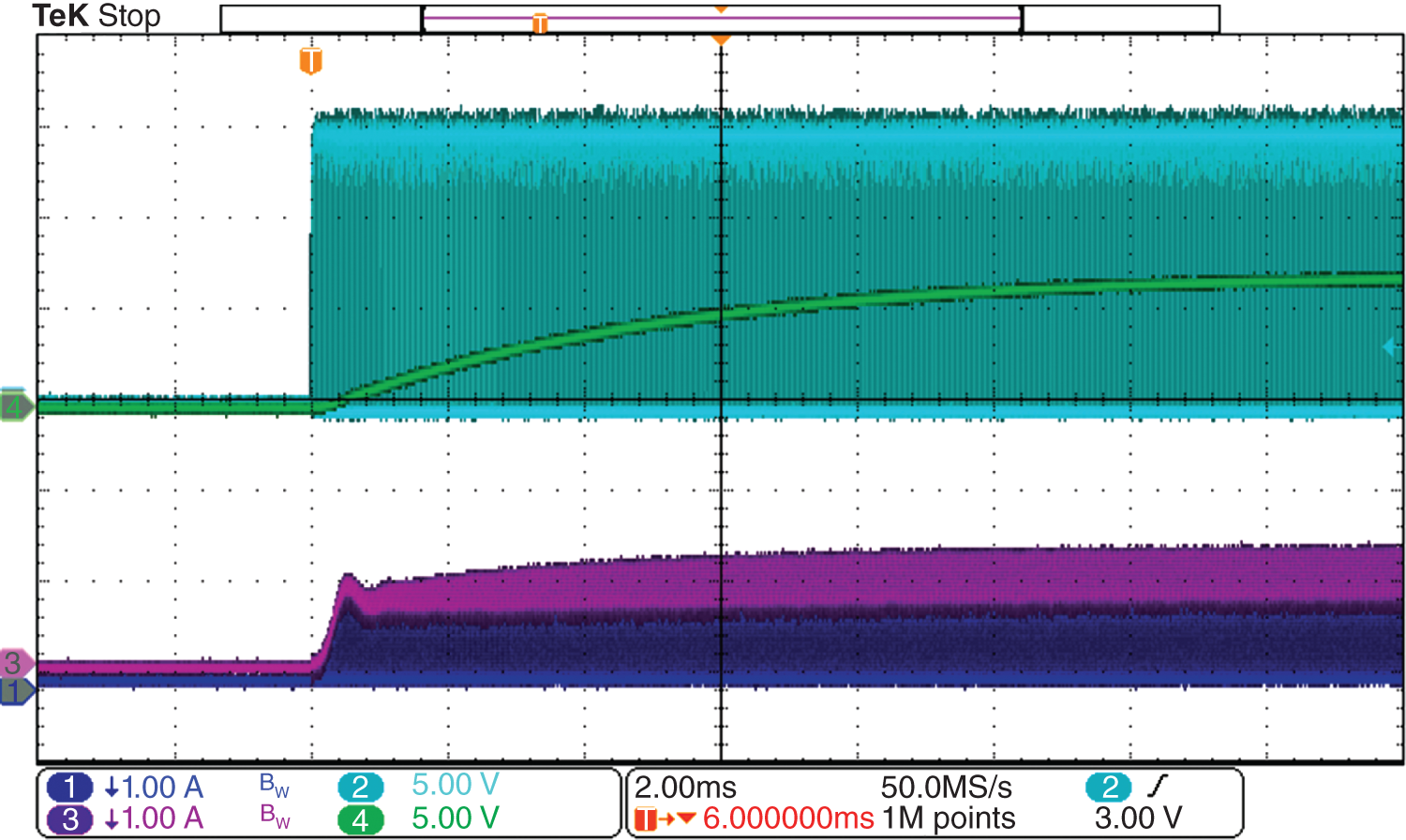
FIGURE 4.32A Workbench hardware results for a step change in reference voltage: (1) input current, (2) switch-node voltage, (3) inductor current, and (4) output voltage. For clarity, see the waveforms in color in the Appendix on the accompanying website.
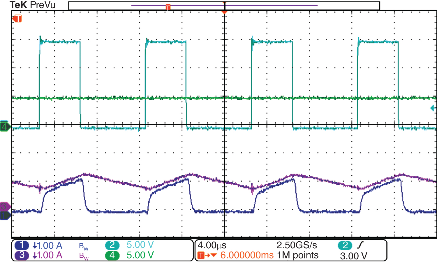
FIGURE 4.32B Workbench hardware results—switching cycle waveforms: (1) input current, (2) switch-node voltage, (3) inductor current, and (4) output voltage.
4.6 FEEDBACK CONTROLLER DESIGN IN DCM
In Sections 4.4 and 4.5, feedback controllers were designed for CCM operation of the converters. The procedure for designing controllers in DCM is the same, except that the average model of the power stage in LTspice simulations can be simply replaced by its model, which is also valid in DCM, as described in Chapter 3. This is illustrated for a buck-boost converter in the LTspice schematic of Figure 4.33, where the average model of the switching pole is valid for both CCM and DCM modes.

FIGURE 4.33 LTspice circuit for the buck-boost converter in both CCM and DCM modes.
The Bode plot of the power stage ![]() in Figure 4.34 shows that in the DCM mode, as compared to the CCM mode, the phase plot appears as if one of the poles in the transfer function cancels out, making it easier to design the feedback controller in this mode.
in Figure 4.34 shows that in the DCM mode, as compared to the CCM mode, the phase plot appears as if one of the poles in the transfer function cancels out, making it easier to design the feedback controller in this mode.

FIGURE 4.34 The gain and phase of the power stage  in CCM and DCM.
REFERENCES
- 1. PWM Controller ICs: Digital power control drivers & powertrain modules product selection | TI.com. https://www.ti.com/power-management/digital-power/digital-power-control-drivers-powertrain-modules/products.html.
- 2. H. Dean Venable, “The K-Factor: A New Mathematical Tool for Stability Analysis and Synthesis,” Proceedings of Powercon 10. http://www.venable.biz.
- 3. Buck Converter Voltage-mode Control Lab Manual. https://sciamble.com/resources/pe-drives-lab/basic-pe/buck-voltage-mode-control.
- 4. Buck-Boost Converter Current-mode Control Lab Manual. https://sciamble.com/resources/pe-drives-lab/basic-pe/buck-boost-current-mode-control.
PROBLEMS
- 4.1 In Example 4.3, plot the gain and the phase of the open-loop transfer function
 .
. - 4.2 In a voltage mode-controlled DC-DC converter the loop transfer function has the crossover frequency
 . The power stage transfer function has a phase angle of
  at the crossover frequency. Calculate
  and
and  in the voltage controller transfer function of Equation (4.18), if the required phase margin is
  .
. - 4.3 In the above problem the power stage has a gain equal to 20 at the crossover frequency,
 , and
, and  . Calculate
  in the voltage controller transfer function of Equation (4.18).
 - 4.4 In Example 4.4, plot the gain and the phase of the open-loop transfer function
 .
. - 4.5 In a peak-current-mode-controlled DC-DC converter, the loop crossover frequency in the outer voltage loop is 10 kHz. At this crossover frequency, the power stage in Figure 4.22b has the gain of 0.1, and the phase angle of
 . Calculate
  ,
,  and
and  in the controller transfer function of Equation (4.32) if the desired phase margin is
  .
. - 4.6 Derive the transfer function
 for a buck converter in CCM.
 - 4.7 Derive the transfer function
 for a boost converter in CCM.
 - 4.8 Derive the transfer function
 for a buck-boost converter in CCM.
Simulation Problems
- 4.9 In a buck converter, various parameters are as follows:
 . The capacitor ESR is
  . The input voltage
  , the switching frequency
  , and the output voltage
  .
.- Obtain the Bode plots for the transfer function
 as shown in Figure 4.10 for the values given in this problem.
 - Obtain the gain and the phase of the transfer function
 at the frequency of 1 kHz, which will be chosen as the crossover of the open-loop transfer function
  in the next problem.
- Obtain the Bode plots for the transfer function
- 4.10 In the buck converter of Problem 4.9, design the feedback controller using the voltage mode, as shown in Figure 4.13, where
 and
and  . Choose the open-loop crossover frequency to be 1 kHz (or close to it) and the phase margin of
- This feedback controller is to be simulated using an op-amp, as shown in Figure 4.12. Obtain the output voltage response for a step change in load.
- Repeat part (a) with a phase margin of
 Compare the output voltage response with that of a phase margin of
  .
. - Repeat part (a) with a crossover frequency of 2 kHz and compare the response to that in part (a).
- 4.11 In a buck-boost converter, various parameters are as follows:
 The capacitor ESR is
  . The input voltage
  the switching frequency
  and the switch duty ratio
  .
.- Obtain the Bode plots for the transfer function
 as shown in Figure 4.24 for the values given in this circuit.
 - Obtain the gain and the phase of the transfer function
 in part (a) at the frequency of 5 kHz, which will be chosen as the crossover of the open-loop transfer function
  in the next problem.
- Obtain the Bode plots for the transfer function
- 4.12 In the buck-boost converter of Problem 4.11, design the feedback controller using the peak-current-mode, as shown in Figure 4.26. Choose the open-loop crossover frequency to be 5 kHz (or close to it) and the phase margin of
 .
.- This feedback controller is to be simulated using an op-amp, as shown in Figure 4.26. Obtain various parameters.
- Obtain the output voltage and the inductor current response for a step change in load.
- 4.13 In the buck-boost converter of Problem 4.11, obtain
 under CCM and DCM modes of operation and compare the results.
APPENDIX 4A BODE PLOTS OF TRANSFER FUNCTIONS WITH POLES AND ZEROS
In this section, Bode plots of various transfer functions are presented as a review.
4A.1 A Pole in a Transfer Function
A transfer function with a pole at ![]() is expressed below
is expressed below
whose gain and phase plots in Figure 4A.1 show that the gain beyond the pole frequency of ![]() starts to change at a rate of −20 dB/decade and the phase angle falls to
starts to change at a rate of −20 dB/decade and the phase angle falls to ![]() approximately a decade later.
approximately a decade later.

FIGURE 4A.1 Gain and phase plots of a pole.
4A.2 A Zero in a Transfer Function
The transfer function with a zero at a frequency of ![]() is expressed below:
is expressed below:
whose gain and phase plots in Figure 4A.2 show that the gain beyond the frequency of ![]() starts to rise at a rate of 20 dB/decade and the phase angle rises to
starts to rise at a rate of 20 dB/decade and the phase angle rises to ![]() approximately a decade later.
approximately a decade later.

FIGURE 4A.2 Gain and phase plots of a zero.
4A.3 A Right-Hand-Plane (RHP) Zero in a Transfer Function
In boost and buck-boost DC-DC converters, transfer functions contain a so-called right-hand plane (RHP) zero, with a transfer function expressed below:
whose gain and phase plots in Figure 4A.3 show that the gain beyond the frequency of ![]() starts to rise at a rate of 20 dB/decade while the phase angle drops to
starts to rise at a rate of 20 dB/decade while the phase angle drops to ![]() approximately a decade later. This RHP zero presents special challenges in designing feedback controllers in boost and buck-boost converters, as is discussed in this chapter.
approximately a decade later. This RHP zero presents special challenges in designing feedback controllers in boost and buck-boost converters, as is discussed in this chapter.

FIGURE 4A.3 Gain and phase plots of a right-hand side zero.
4A.4 A Double Pole in a Transfer Function
In DC-DC converter transfer functions, presence of L-C filters introduces a double pole, which can be expressed as below:
 (4A.4)
and whose gain and plots in Figure 4A.4 show that the gain beyond the frequency ![]() starts to fall at a rate of 40
starts to fall at a rate of 40 ![]() and the phase angle falls toward
and the phase angle falls toward ![]() . These plots depend on the damping coefficient
. These plots depend on the damping coefficient ![]() .
.

FIGURE 4A.4 Gain and phase plots of a double pole.
APPENDIX 4B TRANSFER FUNCTIONS IN CONTINUOUS CONDUCTION MODE (CCM)
In this section, we will derive the transfer function v o / d for the three converters operating in CCM
4B.1 Buck Converters
From Figure 4.7, the small-signal diagram for a buck converter is shown in Figure 4B.1. The output stage impedance Zos is defined as the parallel combination of the filter capacitor and the load resistance:

FIGURE 4B.1 Equivalent circuit of average buck converter.
In any practical converter, r << R, and therefore, R + r ≈ R. Making use of this assumption in Equation (4B.1),
Defining Z eff as the sum of the filter inductor impedance sL and the output stage impedance Z os ,
Therefore, in Figure 4B.1, by voltage division,
4B.2 Boost Converter
From Figure 4.7, the small-signal diagram of a boost converter is shown in Figure 4B.2a . In this circuit, the DC steady-state operating point values can be calculated as follows:

FIGURE 4B.2 Equivalent circuit of average boost converter.
Equating the input and the output power,
Substituting (Equation 4B.5) into (Equation 4B.6),
In Figure 4B.2a, the sub-circuit left of the marked terminals can be replaced by its Norton equivalent, as shown in Figure 4B.2b. The sub-circuit left of the transformer in Figure 4B.2b can be transformed to the right, as shown in Figure 4B.2c, where
The two current sources in Figure 4B.2c can be combined and using the Thevenin’s equivalent, the equivalent voltage in Figure 4B.2d is
Using the equivalent voltage in (Equation 4B.9) and applying the voltage division in the circuit of Figure 4B.2d,
4B.3 Buck-Boost Converter
From Figure 4.7, the small-signal diagram of a buck-boost converter is shown in Figure 4B.3a . First, we will calculate the values of the needed quantities at the DC steady-state operating point.
In a buck-boost converter,
Equating the input and the output power,
and hence,
Considering the sub-circuit to the left of the marked terminals in Figure 4B.3a and drawn in Figure 4B.3b,
where
(Equations 4B.16) and (4B.17) are valid in general only if i l = i 2 = 0 . Therefore in Figure 4B.3b,
Shorting the terminals as shown in Figure 4B.3c,
In Figure 4B.3c,
Substituting (Equation 4B.20) into (Equation 4B.19),
From Figures 4B.3b and 4B.3c, and (Equations 4B.18) and (4B.21), the Thevenin impedance to the left of the marked terminals in Figure 4B.3a is
where
With this Thevenin equivalent, the circuit of Figure 4B.3a, can be drawn as shown in Figure 4B.4a.

FIGURE 4B.4A Equivalent circuit of average buck-boost converter (contd.)
The sub-circuit to the left of the marked terminals can be represented by its Norton equivalent, as shown in Figure 4B.4b.

FIGURE 4B.4B Equivalent circuit of average buck-boost converter (contd.)
Combining the current sources and representing the sub-circuit in Figure 4B.4b by its Thevenin equivalent as shown in Figure 4B.4c,

FIGURE 4B.4C Equivalent circuit of average buck-boost converter (contd.)
Hence,
APPENDIX 4C DERIVATION OF PARAMETERS OF THE CONTROLLER TRANSFER FUNCTIONS
4C.1 Controller Transfer Function with One Pole-Zero Pair
The controller transfer function given below consists of a pole at the origin and a pole-zero pair to provide phase boost:
To analyze this transfer function, the pole at the origin can be omitted since we know that it introduces a phase of −90°, by defining another transfer function as follows:
where
4C.1.1 Frequency at which fboosl Occurs
The maximum angle f boosl provided by the controller occurs at the geometric mean of the zero and pole frequencies, as shown below. (This geometric mean frequency is made to coincide with w = w c where wc is the cross-over frequency.) To find the frequency at which f boosl occurs, we will set the derivative of the phase angle to zero.
Therefore,
 (4C.3)
or
From (Equation 4C.5),
which shows that the phase angle of the controller transfer function reaches its maximum at the geometric-mean frequency.
4C.1.2 Deriving the Zero and Pole Frequencies
Substituting (Equation 4C.6) into (Equation 4C.2),
or
Note that ![]() and
and ![]() . Therefore, in (Equation 4C.8),
. Therefore, in (Equation 4C.8),
We will define an intermediate variable, called the K-factor, as
Solving (Equations 4C.9) and (4C.10),
or
4C.1.3 Realizing the Controller Transfer Function with a Single Op-Amp
The controller transfer function in (Equation 4C.1) can be realized by a single op-amp circuit as shown below.
In Figure 4C.1, obtaining the input-output relationship and comparing it with the transfer function of (Equation 4C.1),

FIGURE 4C.1 Controller implementation of −GC (S), using Eq. 4-C1(A), by an op-amp.
From (Equation 4C.13), in terms of Rj
4C.2 Controller Transfer Function with Two Pole-Zero Pairs
The controller transfer function given below consists of a pole at the origin and two pole-zero pairs to provide phase boost
To analyze this transfer function, the pole at the origin can be omitted since we know that it introduces a phase of −90°, by defining another transfer function as follows:
where
A derivation similar to Section 4C.1 shows that the phase peaks at a frequency f c that is the geometric mean of the pole and zero frequencies, similar to that in Section 4C.1:
Next, we will use the trigonometric identity that
and from Equations (4C.17) and (4C.18), at frequency ![]() , the phase boost is
, the phase boost is
 (4C.20)
and using Equations (4C.20) and (4C.21),
The controller transfer function in (Equation 4C.15) can be realized by a single op-amp circuit as shown below.
In Figure 4C.2, obtaining the input-output relationship and comparing it with the transfer function of (Equation 4C.15) in terms of Rj,

FIGURE 4C.2 Controller implementation of −GC(S), using Eq. 4‐C15, by an op‐amp.
 (4C.24)