
Chapter 3
Behavioral Modeling and High-Level Simulation
The analysis of nonideal effects described in Chapter 2 allows us to derive precise equivalent circuits and models for the different ![]() M building blocks. This chapter shows how these models can be used for improving the accuracy and computational efficiency of system-level simulations. This constitutes an essential tool for the systematic design of
M building blocks. This chapter shows how these models can be used for improving the accuracy and computational efficiency of system-level simulations. This constitutes an essential tool for the systematic design of ![]() Ms as will be described in Chapter 4.
Ms as will be described in Chapter 4.
This chapter is organized as follows. Section 3.1 describes the systematic top-down/bottom-up synthesis methodology commonly followed to design ![]() Ms. Section 3.2 compares the different simulation approaches that can be used for the evaluation of
Ms. Section 3.2 compares the different simulation approaches that can be used for the evaluation of ![]() Ms, emphasizing on the benefits of behavioral simulation techniques. Section 3.3 focuses on the behavioral modeling technique and Section 3.4 shows an efficient way of implementing
Ms, emphasizing on the benefits of behavioral simulation techniques. Section 3.3 focuses on the behavioral modeling technique and Section 3.4 shows an efficient way of implementing ![]() M block models in SIMULINK. Finally, Section 3.5 presents SIMSIDES, a time-domain behavioral simulator implemented in the MATLAB/SIMULINK environment that is based on the behavioral modeling techniques described in this chapter. Finally, two case studies are described in Section 3.6 to illustrate the use of SIMSIDES for the high-level sizing and simulation of
M block models in SIMULINK. Finally, Section 3.5 presents SIMSIDES, a time-domain behavioral simulator implemented in the MATLAB/SIMULINK environment that is based on the behavioral modeling techniques described in this chapter. Finally, two case studies are described in Section 3.6 to illustrate the use of SIMSIDES for the high-level sizing and simulation of ![]() Ms.
Ms.
3.1 Systematic Design Methodology of  Modulators
One of the most common approaches used for the systematic design of high-performance ![]() Ms is based on the well-known top-down/bottom-up hierarchical synthesis methodology, conceptually illustrated in Figure 3.1a [1]. In this approach, a given system is divided into several hierarchical levels so that at each abstraction level of the system hierarchy, a design (or sizing) process takes place, thus transmitting (or mapping) the system specifications in a hierarchical way, from the top level to the bottom level. The reverse path in Figure 3.1a corresponds to the hierarchical bottom-up verification process of the system performance [2].
Ms is based on the well-known top-down/bottom-up hierarchical synthesis methodology, conceptually illustrated in Figure 3.1a [1]. In this approach, a given system is divided into several hierarchical levels so that at each abstraction level of the system hierarchy, a design (or sizing) process takes place, thus transmitting (or mapping) the system specifications in a hierarchical way, from the top level to the bottom level. The reverse path in Figure 3.1a corresponds to the hierarchical bottom-up verification process of the system performance [2].
Figure 3.1 Hierarchical synthesis methodology: (a) Conceptual block diagram and (b) system partitioning commonly used in ![]() Ms.
Ms.

3.1.1 System Partitioning and Abstraction Levels
Figure 3.1b depicts the hierarchical synthesis methodology that is usually adopted in the design of ![]() Ms. The system is partitioned in the following hierarchical levels [1–5]:
Ms. The system is partitioned in the following hierarchical levels [1–5]:
- Architecture or Topology Level: that is, single-loop or cascade
 M, single-bit or multibit quantization, low-pass or band-pass, DT or CT implementation, etc.
 - Subcircuit or Building-Block Level: that is, amplifiers, transconductors, comparators, capacitors, resistors, switches, etc.
- Cell Level: that is, the circuit topology of a given building block, for instance folded-cascode or telescopic cascode OTA, SC or current-steering DAC, nMOS or CMOS switches, etc.
- Physical Level: which covers from transistor-level schematics to the layout and chip implementation.
The design process of a ![]() M starts from the system-level specifications, that is, the effective resolution (ENOB) and the signal bandwidth (
M starts from the system-level specifications, that is, the effective resolution (ENOB) and the signal bandwidth (![]() ). The first goal is to find out the best modulator topology that fulfills these specifications with minimum power dissipation. To this purpose, initial ideal design equations of NTF and IBN—which are based on a linear model of the embedded quantizers as described in Chapter 1—are used for calculating approximate values for the main
). The first goal is to find out the best modulator topology that fulfills these specifications with minimum power dissipation. To this purpose, initial ideal design equations of NTF and IBN—which are based on a linear model of the embedded quantizers as described in Chapter 1—are used for calculating approximate values for the main ![]() M parameters, that is, OSR,
M parameters, that is, OSR, ![]() , and
, and ![]() . Once these parameters are known, the architecture topology can be synthesized using more accurate nonlinear model equations. To this purpose, Schreier's MATLAB Delta-Sigma toolbox [6, 7] is widely used in the
. Once these parameters are known, the architecture topology can be synthesized using more accurate nonlinear model equations. To this purpose, Schreier's MATLAB Delta-Sigma toolbox [6, 7] is widely used in the ![]() community. Usually, there are several topologies which are a priori good candidates to meet a given set of modulator specifications.
community. Usually, there are several topologies which are a priori good candidates to meet a given set of modulator specifications.
In order to determine the best ![]() M architecture, some analytical procedures are normally used for estimating the power consumption of the different
M architecture, some analytical procedures are normally used for estimating the power consumption of the different ![]() M topologies [8]. These procedures are based on compact expressions of the in-band noise power, similar to those derived in Chapter 2, which contemplate both architectural and technological features, and include the impact of some critical circuit errors such as thermal noise, finite OTA DC gain (or equivalent), and incomplete settling (GB and SR). Recent works demonstrate that nonlinearities can be efficiently incorporated in the Schreier's toolbox in order to fine tune this architectural exploration procedure [9].
M topologies [8]. These procedures are based on compact expressions of the in-band noise power, similar to those derived in Chapter 2, which contemplate both architectural and technological features, and include the impact of some critical circuit errors such as thermal noise, finite OTA DC gain (or equivalent), and incomplete settling (GB and SR). Recent works demonstrate that nonlinearities can be efficiently incorporated in the Schreier's toolbox in order to fine tune this architectural exploration procedure [9].
On the basis of the system-level estimation of the power consumption, a ranking of different candidate ![]() M architectures can be determined in order to decide the most suitable topology. Other important criteria at this step are the sensitivity to circuit element tolerances and mismatch (especially important in CT cascade topologies), the modulator loop-filter stability (particularly critical in high-order single-loop topologies), and/or the impact of the feedback DAC nonlinearity in multibit
M architectures can be determined in order to decide the most suitable topology. Other important criteria at this step are the sensitivity to circuit element tolerances and mismatch (especially important in CT cascade topologies), the modulator loop-filter stability (particularly critical in high-order single-loop topologies), and/or the impact of the feedback DAC nonlinearity in multibit ![]() Ms.
Ms.
3.1.2 Sizing Process
Once the modulator architecture has been selected, the next step consists of mapping the modulator-level specifications (ENOB and ![]() ) onto building-block specifications, that is, amplifier finite DC gain, output swing, GB, SR, etc. In this system-level design process—commonly referred to as high-level sizing—the design parameters are the electrical specifications of the different
) onto building-block specifications, that is, amplifier finite DC gain, output swing, GB, SR, etc. In this system-level design process—commonly referred to as high-level sizing—the design parameters are the electrical specifications of the different ![]() M subcircuits, namely, amplifiers, transconductors (in CT-
M subcircuits, namely, amplifiers, transconductors (in CT-![]() Ms), comparators, switches, and passive elements, that is, capacitors, resistors, and even inductors in the case of some BP-
Ms), comparators, switches, and passive elements, that is, capacitors, resistors, and even inductors in the case of some BP-![]() Ms [10]. The result of this multidimensional design space exploration constitutes the start point of the electrical or cell-level sizing process where, after selecting the appropriate topology for every
Ms [10]. The result of this multidimensional design space exploration constitutes the start point of the electrical or cell-level sizing process where, after selecting the appropriate topology for every ![]() M subcircuit, the corresponding transistor sizes and bias currents are obtained.
M subcircuit, the corresponding transistor sizes and bias currents are obtained.
Therefore, as shown in Figure 3.1b, the design methodology of ![]() Ms can be essentially divided into two main sizing processes: high-level sizing and cell-level sizing. Both of them are tasks that require a multitude of redesign iterations until the specifications at each level are met [11]. This procedure is conceptually depicted in Figure 3.2 [5]. At each iteration the performance of the circuit is evaluated at a given point of the design space, the design parameters are modified according to such an evaluation, and the procedure is repeated. Note that, although this procedure is the same in both high-level sizing and cell-level sizing, the design problem and its formulation is different in both cases. High-level sizing is a system-level synthesis process where the inputs variables are the system-level (modulator) specifications and the output variables are the building-block electrical specifications (design parameters). The latter specifications constitute the input variables for the cell-level sizing process.
Ms can be essentially divided into two main sizing processes: high-level sizing and cell-level sizing. Both of them are tasks that require a multitude of redesign iterations until the specifications at each level are met [11]. This procedure is conceptually depicted in Figure 3.2 [5]. At each iteration the performance of the circuit is evaluated at a given point of the design space, the design parameters are modified according to such an evaluation, and the procedure is repeated. Note that, although this procedure is the same in both high-level sizing and cell-level sizing, the design problem and its formulation is different in both cases. High-level sizing is a system-level synthesis process where the inputs variables are the system-level (modulator) specifications and the output variables are the building-block electrical specifications (design parameters). The latter specifications constitute the input variables for the cell-level sizing process.
Figure 3.2 Iterative procedure usually followed for high-level sizing and cell-level sizing.

The design parameter selection in Figure 3.2 can be carried out “manually,” that is, the entire design space is searched by considering all possible combinations of design parameters. In this case, once the whole design space has been completely explored and checked, the best design can be selected among those that meet the required specifications with the lowest (estimated) power dissipation and area. However, this “vast force” search approach is quite inefficient—and even unfeasible in many cases—in terms of computational resources and CPU time.1 Instead, an optimization engine is normally used for guiding the exploration of the design space. To this purpose, diverse algorithms such as simulated annealing [12] or genetic algorithms [4] may be used for the optimization. Usually, the same optimization methodology—normally based on the formulation and minimization of a design-oriented cost function—is used in both sizing tasks, that is, high-level sizing and cell-level sizing [3].
Different performance-evaluation strategies can be followed in Figure 3.2. Essentially, the cost function can be evaluated by means of equations or simulations [1]. Although the former is much faster than the latter, the accuracy of the results strongly depends on the topology, that is, the ![]() M architecture (for high-level sizing) and the circuit schematic (for cell-level sizing). For that reason, the most common approach followed by the
M architecture (for high-level sizing) and the circuit schematic (for cell-level sizing). For that reason, the most common approach followed by the ![]() M community has been based on using simulation as performance evaluation [3–5, 13–19]. However, in contrast to the optimization process—which is used in both sizing tasks—a different simulation approach is considered to evaluate the performance of either the entire (system-level) modulator or just a single building block, such as an amplifier or a comparator (cell-level). The latter can be analyzed using an electrical (SPICE-like) simulator with a high degree of accuracy and computational efficiency. On the contrary, the evaluation of the system-level (modulator) performance can be carried out following different simulation approaches discussed in the next section.
M community has been based on using simulation as performance evaluation [3–5, 13–19]. However, in contrast to the optimization process—which is used in both sizing tasks—a different simulation approach is considered to evaluate the performance of either the entire (system-level) modulator or just a single building block, such as an amplifier or a comparator (cell-level). The latter can be analyzed using an electrical (SPICE-like) simulator with a high degree of accuracy and computational efficiency. On the contrary, the evaluation of the system-level (modulator) performance can be carried out following different simulation approaches discussed in the next section.
3.2 Simulation Approaches for the High-Level Evaluation of  Ms
Ms
The high-level synthesis described above requires performing a large number of simulations. Depending on the design and required specifications, hundreds or even thousands of iterations may be needed. Therefore, in order to make this part of the design feasible, simulations should consume short CPU times. This is particularly critical in the case of ![]() Ms because of their nonlinear oversampled-data nature. For that reason, in order to compute the IBN power at the output of a
Ms because of their nonlinear oversampled-data nature. For that reason, in order to compute the IBN power at the output of a ![]() M with enough numerical accuracy, a transient simulation of at least
M with enough numerical accuracy, a transient simulation of at least ![]() clock cycles is usually required.2 Therefore, a transient analysis of a
clock cycles is usually required.2 Therefore, a transient analysis of a ![]() M using common transistor-level (SPICE-like) circuit simulation is too slow for allowing an efficient space exploration, regardless of whether it is performed by a manual parameter sweeps or guided by an optimizer. As an example, a
M using common transistor-level (SPICE-like) circuit simulation is too slow for allowing an efficient space exploration, regardless of whether it is performed by a manual parameter sweeps or guided by an optimizer. As an example, a ![]() -point transient analysis in HSPICE of a cascade 2-1 SC-
-point transient analysis in HSPICE of a cascade 2-1 SC-![]() M including the clock-phase generator and other auxiliary subcircuits takes over 85 h CPU time in a 2.2-GHz core with 4-GB RAM. This means that a synthesis process based on this performance-evaluation approach would take months or even years! Hence, transistor-level simulation is obviously computationally unfeasible for synthesis purposes, and it is normally used only for the final design verification, as will be discussed in Chapter 4 [19].
M including the clock-phase generator and other auxiliary subcircuits takes over 85 h CPU time in a 2.2-GHz core with 4-GB RAM. This means that a synthesis process based on this performance-evaluation approach would take months or even years! Hence, transistor-level simulation is obviously computationally unfeasible for synthesis purposes, and it is normally used only for the final design verification, as will be discussed in Chapter 4 [19].
In addition to the long CPU times required to simulate a ![]() M at transistor level, another practical issue associated with this simulation approach is related to the convergence problems that typically arise in electrical simulators such as HSPICE [21] or Spectre [22]. Moreover, transistor-level simulation is not a suited simulation method for the high-level sizing process because the design parameters—that is, device sizes and biasing—are hierarchically far from system-level specifications. Hence, it is quite difficult for a designer to get an insight into what is happening at the system level by running simulations based on transistor-level models, as the impact of a given transistor width or length has a direct impact on many different performance metrics of
M at transistor level, another practical issue associated with this simulation approach is related to the convergence problems that typically arise in electrical simulators such as HSPICE [21] or Spectre [22]. Moreover, transistor-level simulation is not a suited simulation method for the high-level sizing process because the design parameters—that is, device sizes and biasing—are hierarchically far from system-level specifications. Hence, it is quite difficult for a designer to get an insight into what is happening at the system level by running simulations based on transistor-level models, as the impact of a given transistor width or length has a direct impact on many different performance metrics of ![]() M building blocks. For instance, the size of the input differential-pair transistor of an OTA affects the values of finite DC gain, nonlinearity, input parasitic capacitance, GB, etc.
M building blocks. For instance, the size of the input differential-pair transistor of an OTA affects the values of finite DC gain, nonlinearity, input parasitic capacitance, GB, etc.
3.2.1 Alternatives to Transistor-Level Simulation
The above-mentioned reasons suggest that increasing the abstraction level of the simulation approach is mandatory to both speed up the simulations and work with design parameters that are closer to the system-level specifications. However, the price to pay for increasing the abstraction level (and consequently the simulation speed) is the loss of accuracy. This problem has motivated the exploration of different simulation approaches in order to optimize the trade-off between CPU time and precision—conceptually illustrated in Figure 3.3 [4].
Figure 3.3 Comparison of simulation approaches in terms of CPU time and accuracy.

An alternative to the transistor-level simulation approach that also runs on electrical simulators consists of using circuit macromodels. These macromodels are usually implemented as equivalent circuits based on ideal voltage- and current-controlled sources that allow to model the main nonideal effects. This approach has the advantage that it can be combined with transistor-level schematics using the same (electrical) simulator. Thus, critical parts of the system can be modeled at transistor level, whereas the remaining ones can be modeled less accurately with macromodels, leading to what is commonly known as a multilevel simulation
technique [2]. Obviously, the simulation CPU time will increase with the number of parts being modeled at transistor level. Therefore, in most practical cases, the use of this approach does not imply a significant improvement with respect to the full transistor-level simulation approach.3
As an example, Table 3.1 compares the CPU times required to simulate a fourth-order single-loop ![]() M in Cadence Spectre circuit simulator, considering
M in Cadence Spectre circuit simulator, considering ![]() -point transient analysis with moderate setting [22]. The modulator topology consists of a cascade of resonators with feed-forward summation (Figure 1.31b). This architecture requires five amplifiers to implement the four loop-filter integrators and the active adder. Simulations were carried out considering ideal macromodels for the switches and the digital blocks (including the clock-phase generator). It can be noted from Table 3.1 that the CPU time increases by approximately 30–40 min with every additional amplifier that is simulated considering a transistor-level implementation. The overall CPU time goes from 45 min required to simulate the entire system with macromodels to 4 h when all amplifiers are implemented at transistor level. These CPU times are more than doubled if conservative mode option is considered in the simulation; over 8 h are required to complete the simulation.
-point transient analysis with moderate setting [22]. The modulator topology consists of a cascade of resonators with feed-forward summation (Figure 1.31b). This architecture requires five amplifiers to implement the four loop-filter integrators and the active adder. Simulations were carried out considering ideal macromodels for the switches and the digital blocks (including the clock-phase generator). It can be noted from Table 3.1 that the CPU time increases by approximately 30–40 min with every additional amplifier that is simulated considering a transistor-level implementation. The overall CPU time goes from 45 min required to simulate the entire system with macromodels to 4 h when all amplifiers are implemented at transistor level. These CPU times are more than doubled if conservative mode option is considered in the simulation; over 8 h are required to complete the simulation.
Table 3.1 CPU time required to simulate a fourth-order single-loop ![]() M considering different situations in a multilevel approach
M considering different situations in a multilevel approach
| Simulation | CPU Time | CPU Time |
| Approach | (moderate mode) | (conservative mode) |
| All opamps macromodeled | 45 min | 2 h |
| One transistor-level opamp | 1 h, 20 min | 4 h |
| Two transistor-level opamps | 2 h | 5 h, 30 min |
| Five transistor-level opamps | 4 h | 8 h, 20 min |
Simulations were carried out in a SUN Fire X2200 M2 server with 4-GB RAM and a 2.2-GHz Dual Core AMD Opteron CPU, running a 64-bit Linux operating system.
As stated above, it is important to mention that the data in Table 3.1 does not account for the time consumed to simulate the digital part of the system—that is, feedback DAC, DEM, clock-phase generator, digital output buffers, etc.—that was considered ideal in these simulations. If transistor-level implementation is considered for those circuits, the overall CPU time for a conservative simulation mode is increased up to one day or even more. Under these conditions, a ![]() -point transient simulation would take over three days CPU time!
-point transient simulation would take over three days CPU time!
3.2.2 Event-Driven Behavioral Simulation Technique
As illustrated in Figure 3.3, the best trade-off between accuracy and speed is achieved by the so-called event-driven behavioral simulation technique [14]. In this approach—conceptually illustrated in Figure 3.4—the modulator is partitioned into a set of subcircuits—often called basic or building blocks—with independent functionality [1, 12]. In ![]() Ms, the most important building blocks are integrators and resonators,4 and the embedded quantizers, made up of an ADC and a DAC. The behavioral modeling technique thus consists in describing each of these building blocks by a model, often referred to as a behavioral model or behavioral law, that emulates their actual operation and takes into account the effect of the main nonideal circuit error mechanisms described in Chapter 2.
Ms, the most important building blocks are integrators and resonators,4 and the embedded quantizers, made up of an ADC and a DAC. The behavioral modeling technique thus consists in describing each of these building blocks by a model, often referred to as a behavioral model or behavioral law, that emulates their actual operation and takes into account the effect of the main nonideal circuit error mechanisms described in Chapter 2.
Figure 3.4 Conceptual block diagram of the behavioral modeling and simulation process.

Note that, strictly speaking, the definition given above for a behavioral model does not necessarily imply that the model is implemented by equations. Indeed, there is an alternative approach that consists of using the so-called table look-up models [23, 24]. The idea behind these models is based on extracting the input–output characteristics of a given building block from electrical simulations and then mapping the extracted information in the form of tables which are used for modeling the functionality of that building block. This way, those tables are used as an alternative to the original transistor-level circuits to accelerate the simulations with a high degree of accuracy. However, the price to pay is the loss of generality and of reusability of the models because they strongly depend on the circuit topology. Indeed, new tables have to be generated whenever the architecture itself or any circuit parameter is modified.
For the aforementioned reasons, table look-up methodologies are more suited for bottom-up verification than for high-level synthesis. Indeed, the most commonly used behavioral modeling approach is based on finite-difference equations. These equations describe the functionality of building blocks by expressing their output signals in terms of their internal state variables and their input signals. Therefore, the accuracy of the behavioral simulation strongly depends on how precisely those equations describe the actual behavior of the corresponding ![]() M subcircuit [5, 15, 19].
M subcircuit [5, 15, 19].
3.2.3 Programming Languages and Behavioral Modeling Platforms
Behavioral models and the corresponding simulation engine (Figure 3.4) can be codified and implemented in a number of platforms using different programming/modeling languages such as C. The latter is a general purpose and universal language that presents high flexibility in describing behavioral models and allowing implementation of behavioral simulation tools in many different operating systems and platforms. Early approaches for the behavioral-level simulation of ![]() Ms were completely compiled in C language, demonstrating to be very appropriate for fast simulation and high-level synthesis of
Ms were completely compiled in C language, demonstrating to be very appropriate for fast simulation and high-level synthesis of ![]() Ms [12].
Ms [12].
The main disadvantage of C-coded behavioral modeling and simulation is that it is restricted to a limited number of building-block models—that is, those included in the corresponding (previously programmed) libraries—thus reducing the kind of ![]() M architectures that can be simulated. From this point of view, this approach is not flexible because building-block models cannot be easily modified and the extension to new building blocks and architectures is constrained by the capabilities of the simulation engine, as well as by the designer skills on C programming language. This may explain why the majority of reported C-based behavioral simulators are intended to simulate SC-
M architectures that can be simulated. From this point of view, this approach is not flexible because building-block models cannot be easily modified and the extension to new building blocks and architectures is constrained by the capabilities of the simulation engine, as well as by the designer skills on C programming language. This may explain why the majority of reported C-based behavioral simulators are intended to simulate SC-![]() Ms [4, 12].
Ms [4, 12].
In order to overcome all these problems, several alternative approaches have been followed to implement behavioral models. One approach that has gained popularity with ![]() M designers is based on the use of standard hardware description languages (HDL), such as either VHDL [25] and its analog extensions [26] or Verilog and Verilog AMS [19]. As will be shown in Chapter 4, VHDL-based behavioral model descriptions can be combined with HDL models of other analog, digital, and mixed-signal circuits, and they can be integrated in the design flow of commercial design environments such as Cadence Design FrameWork II [27].
M designers is based on the use of standard hardware description languages (HDL), such as either VHDL [25] and its analog extensions [26] or Verilog and Verilog AMS [19]. As will be shown in Chapter 4, VHDL-based behavioral model descriptions can be combined with HDL models of other analog, digital, and mixed-signal circuits, and they can be integrated in the design flow of commercial design environments such as Cadence Design FrameWork II [27].
An alternative and widely used approach for the behavioral modeling and simulation of ![]() Ms consists of using the MATLAB/SIMULINK platform [28, 29]. This well-known mathematical software—which constitutes a standard CAD platform today in science and engineering—presents a number of advantages in terms of friendliness of the user interface: flexibility for the extension of building blocks library and for the simulation of either DT or CT systems, good trade-off between accuracy and simulation speed, and a direct access to very powerful tools for signal postprocessing [5, 15].
Ms consists of using the MATLAB/SIMULINK platform [28, 29]. This well-known mathematical software—which constitutes a standard CAD platform today in science and engineering—presents a number of advantages in terms of friendliness of the user interface: flexibility for the extension of building blocks library and for the simulation of either DT or CT systems, good trade-off between accuracy and simulation speed, and a direct access to very powerful tools for signal postprocessing [5, 15].
The rest of this chapter is devoted to the behavioral modeling and simulation of ![]() Ms in the MATLAB/SIMULINK environment, explaining the different approaches to model
Ms in the MATLAB/SIMULINK environment, explaining the different approaches to model ![]() M building blocks and how to use these models for the efficient simulation of
M building blocks and how to use these models for the efficient simulation of ![]() Ms.
Ms.
3.3 Implementing  M Behavioral Models
The analysis of error mechanisms in ![]() Ms allows designers to obtain a set of closed-form expressions that shows the degradation caused by circuit-level electrical parameters at different levels of the modulator hierarchy. On the one hand, the analytical procedure described in Chapter 2 is used for propagating the effect of errors from the building-block (either integrator or resonator) transfer function to the modulator NTF, in order to obtain the
Ms allows designers to obtain a set of closed-form expressions that shows the degradation caused by circuit-level electrical parameters at different levels of the modulator hierarchy. On the one hand, the analytical procedure described in Chapter 2 is used for propagating the effect of errors from the building-block (either integrator or resonator) transfer function to the modulator NTF, in order to obtain the ![]() M performance metrics, that is, IBN and SNDR. As stated in Section 3.1, simplified versions of these equations relating architectural parameters (
M performance metrics, that is, IBN and SNDR. As stated in Section 3.1, simplified versions of these equations relating architectural parameters (![]() ,
, ![]() , and
, and ![]() ) to circuit-level errors are very appropriate for initial system-level estimations of the power consumption and preliminary architecture selection. On the other hand, precise equations describing the functionality of building blocks as a function of error parameters constitute the basis for building accurate behavioral models. To this end, those equations must be transformed into computational flowcharts that can be implemented by programming languages. This procedure is illustrated in the next section for two basic building blocks: an SC FE integrator and a Gm-C integrator. These two circuits are basic building blocks of SC- and CT-
) to circuit-level errors are very appropriate for initial system-level estimations of the power consumption and preliminary architecture selection. On the other hand, precise equations describing the functionality of building blocks as a function of error parameters constitute the basis for building accurate behavioral models. To this end, those equations must be transformed into computational flowcharts that can be implemented by programming languages. This procedure is illustrated in the next section for two basic building blocks: an SC FE integrator and a Gm-C integrator. These two circuits are basic building blocks of SC- and CT-![]() Ms, respectively.5
Ms, respectively.5
3.3.1 From Circuit Analysis to Computational Algorithms
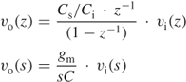
Figure 3.5 shows the conceptual (single-ended) schematic of an SC FE integrator (Figure 3.5a) and a Gm-C integrator (Figure 3.5b). Considering ideal circuit elements, the output voltage ![]() of Figure 3.5a is given by the following finite-difference equation:
of Figure 3.5a is given by the following finite-difference equation:
where ![]() is the input voltage,
is the input voltage, ![]() and
and ![]() are, respectively, the sampling and integration capacitors, and
are, respectively, the sampling and integration capacitors, and ![]() stands for the
stands for the ![]() th sampling time instant, with
th sampling time instant, with ![]() being the sampling period.
being the sampling period.
Figure 3.5 Conceptual schematic of: (a) an SC FE integrator and (b) a Gm-C integrator.

Note that Equation 3.1 is easy to solve numerically because the value of the output voltage at a given time instant ![]() can be computed by adding the value of the output at the previous sampling period
can be computed by adding the value of the output at the previous sampling period ![]() and the value of the input voltage at
and the value of the input voltage at ![]() multiplied by
multiplied by ![]() . This operation is conceptually represented by the flowchart shown in Figure 3.6 and can be expressed in a computational model as follows:
. This operation is conceptually represented by the flowchart shown in Figure 3.6 and can be expressed in a computational model as follows:
vinit=0;
Cs=1e‐12;
Ci=1e‐12;
n=1;
nfinal=10;
vi(1:10)=1;
vo(1)=vinit;
while n<=nfinal
    n=n+1;
    vo(n)=vo(n‐1)+Cs/Ci*vi(n‐1);
end;
Figure 3.6 Flowchart used for computing behavioral Equation 3.1.

where vinit stands for the initial condition, nfinal stands for the final sampling instant, and ![]() pF has been assumed.6 A while statement has been considered, although other iterative statements such as if or for can be used as well.
pF has been assumed.6 A while statement has been considered, although other iterative statements such as if or for can be used as well.
The ideal functionality of Figure 3.5b can be mathematically expressed by the following differential equation:
where ![]() is the transconductance and
is the transconductance and ![]() is the integration capacitance. The above expression can be integrated by MATLAB/SIMULINK solvers very efficiently [28].
is the integration capacitance. The above expression can be integrated by MATLAB/SIMULINK solvers very efficiently [28].
The ideal models described for SC and CT integrators in the time domain can be implemented very easily in the frequency domain using SIMULINK elementary library blocks [29] as illustrated in Figure 3.7. The corresponding transfer functions can be obtained by applying a ![]() -transform and an
-transform and an ![]() -transform to Equations 3.1 and 3.2, respectively, giving
-transform to Equations 3.1 and 3.2, respectively, giving
where ![]() and
and ![]() stand for the
stand for the ![]() -transforms of
-transforms of ![]() and
and ![]() in Figure 3.5a and
in Figure 3.5a and ![]() and
and ![]() are the
are the ![]() -transforms of
-transforms of ![]() and
and ![]() in Figure 3.5b. Both models can be computed very efficiently using the discrete-time and continuous-time solvers provided in the SIMULINK software [29].
in Figure 3.5b. Both models can be computed very efficiently using the discrete-time and continuous-time solvers provided in the SIMULINK software [29].
Figure 3.7 Ideal SIMULINK models of the integrators shown in Figure 3.5.

3.3.2 Time-Domain versus Frequency-Domain Behavioral Models
The ideal behavioral models described can be either represented in the time domain by Equations 3.1 and 3.2 or in the frequency domain by Equation 3.3. There is an exact correspondence between both of them, giving rise to identical results. Indeed, provided that the ![]() M building blocks can be treated as LTI systems, the most convenient (and simplest) way of modeling their behavior is using frequency-domain transfer functions. However, this is not very useful in most practical situations because, as stated in Chapter 2, the performance of
M building blocks can be treated as LTI systems, the most convenient (and simplest) way of modeling their behavior is using frequency-domain transfer functions. However, this is not very useful in most practical situations because, as stated in Chapter 2, the performance of ![]() Ms is degraded by the effect of circuit-level errors. As shown in this chapter, the majority of circuit errors are modeled in a more accurate way if behavioral models are described in the time domain instead of in the frequency domain.
Ms is degraded by the effect of circuit-level errors. As shown in this chapter, the majority of circuit errors are modeled in a more accurate way if behavioral models are described in the time domain instead of in the frequency domain.
As an example, let us consider the effect of OTA finite DC gain on the integrators in Figure 3.5. This effect can be modeled as shown in Figure 3.8, where ![]() stands for the finite DC voltage gain of the opamp in the SC FE integrator and
stands for the finite DC voltage gain of the opamp in the SC FE integrator and ![]() is the finite output conductance of the transconductor in the Gm-C integrator, such that the finite DC gain is given by
is the finite output conductance of the transconductor in the Gm-C integrator, such that the finite DC gain is given by ![]() . The time-domain equations describing the behavior of the integrators in Figure 3.8 are given by
. The time-domain equations describing the behavior of the integrators in Figure 3.8 are given by

where ![]() and
and ![]() . Note that the behavioral model of the SC integrator with finite DC gain can be computed using a flowchart similar to the ideal one shown in Figure 3.6 by simply modifying the corresponding multiplication factors of
. Note that the behavioral model of the SC integrator with finite DC gain can be computed using a flowchart similar to the ideal one shown in Figure 3.6 by simply modifying the corresponding multiplication factors of ![]() and
and ![]() according to Equation 3.4. In the case of CT integrators, the corresponding differential equation can be numerically solved using either C or MATLAB code as programming language.7
according to Equation 3.4. In the case of CT integrators, the corresponding differential equation can be numerically solved using either C or MATLAB code as programming language.7
Figure 3.8 Modeling OTA finite DC gain in: (a) SC FE integrators and (b) Gm-C integrators.

Operating in a similar way as in the previous section, the (frequency-domain) transfer functions of both circuits in Figure 3.8 can be obtained yielding

The above-mentioned transfer functions can be easily modeled using elementary blocks of the SIMULINK library as shown in Figure 3.9. However, as stated above, frequency-domain models are not useful when several nonideal and nonlinear effects are considered.8 Instead, a time-domain model considering the operation during different clock phases is more accurate to include different circuit-level phenomena. In order to illustrate this, let us analyze the circuit in Figure 3.8a in both clock phases, ![]() and
and ![]() .
.
Figure 3.9 Modeling the effect of finite DC gain on the integrators transfer function in SIMULINK.

At the end of clock phase ![]() (sampling phase) of period
(sampling phase) of period ![]() the sampling capacitor
the sampling capacitor ![]() and the integration capacitor
and the integration capacitor ![]() are charged at the following voltages, respectively,
are charged at the following voltages, respectively,
where ![]() denotes the voltage at the output of the opamp in Figure 3.8a.
denotes the voltage at the output of the opamp in Figure 3.8a.
At the end of clock phase ![]() (integration phase) of period
(integration phase) of period ![]() the voltages across
the voltages across ![]() and
and ![]() are, respectively, given by
are, respectively, given by
The charge-balance equation at the negative input node of the opamp in Figure 3.8a can be written as
Replacing Equations 3.6 and 3.7 into Equation 3.8 gives
Taking into account that ![]() , the above expression transforms into the SC part of Equation 3.4, which after taking the
, the above expression transforms into the SC part of Equation 3.4, which after taking the ![]() -transform results in Equation 3.5.
-transform results in Equation 3.5.
Note that the charge-balance analysis described in Equations 3.8 is more complex than using ![]() -domain transfer functions to model simple phenomena, such as the ideal behavior of simple building blocks and/or the effect of linear errors, such as finite DC gain. However, as the model becomes more accurate including more nonideal circuit errors and/or nonlinearities, the charge-balance model is the most suitable approach to be implemented in a behavioral simulator. As an illustration, let us assume the voltage dependence of the finite DC gain in SC FE integrators.9 This nonlinear effect can be modeled by replacing the voltage linear gain
-domain transfer functions to model simple phenomena, such as the ideal behavior of simple building blocks and/or the effect of linear errors, such as finite DC gain. However, as the model becomes more accurate including more nonideal circuit errors and/or nonlinearities, the charge-balance model is the most suitable approach to be implemented in a behavioral simulator. As an illustration, let us assume the voltage dependence of the finite DC gain in SC FE integrators.9 This nonlinear effect can be modeled by replacing the voltage linear gain ![]() parameter in Figure 3.8a by a nonlinear function of the output voltage
parameter in Figure 3.8a by a nonlinear function of the output voltage ![]() , where
, where ![]() represents the
represents the ![]() th-order nonlinear voltage-gain coefficient [31]. Taking these nonlinear effects into account, the charge-balance equations transform into the following ones:
th-order nonlinear voltage-gain coefficient [31]. Taking these nonlinear effects into account, the charge-balance equations transform into the following ones:

where ![]() and
and ![]() .
.
From Equations 3.9 and 3.10, it can be shown that the nonlinear finite-difference equation describing the behavior of the integrator can be written as

Note that an iterative procedure is needed to compute the behavioral model in Equation 3.11, because the output voltage of the opamp ![]() depends on the amplifier nonlinear gain, which in turns changes with
depends on the amplifier nonlinear gain, which in turns changes with ![]() .
.
3.3.3 Implementing Time-Domain Behavioral Models in MATLAB
The behavioral model described by Equations 3.10 and 3.11 can be programmed using a so-called M-file [28] with the MATLAB code shown in Figure 3.10, where C1 and C2 are, respectively, the sampling capacitance (![]() ) and integration capacitance (
) and integration capacitance (![]() ), and count is a parameter that determines the clock phase, with count=0 corresponding to the sampling phase and count=1 to the integration phase. This way, as illustrated in Figure 3.11, the clock-phase scheme can be selected to be either the one shown in Figure 3.8a or the complementary one, that is, with the input switch being clocked at
), and count is a parameter that determines the clock phase, with count=0 corresponding to the sampling phase and count=1 to the integration phase. This way, as illustrated in Figure 3.11, the clock-phase scheme can be selected to be either the one shown in Figure 3.8a or the complementary one, that is, with the input switch being clocked at ![]() . The input signal is modeled by a matrix made up of two vectors, u(1) and u(2), while the output is stored in a variable named y, with yold modeling the output sample stored in the previous clock phase and ytemp being a temporal state variable used until convergence is achieved.
. The input signal is modeled by a matrix made up of two vectors, u(1) and u(2), while the output is stored in a variable named y, with yold modeling the output sample stored in the previous clock phase and ytemp being a temporal state variable used until convergence is achieved.
Figure 3.10 MATLAB code for the behavioral model of the SC FE integrator in Figure 3.8a including the effect of the amplifier gain nonlinearity.

Figure 3.11 Meaning of count in the behavioral model of an SC FE integrator, considering that the input switch clock phase is: (a) ![]() and (b)
and (b) ![]() .
.

Note that the convergence criterion used in the iterative procedure is AVVAR=abs[(AVOLD =AVNEW) /AVNEW] < thrs, where thrs models the threshold value selected for convergence (usually thrs=0.01), abs(x) stands for the absolute value of x, and AVOLD and AVNEW are, respectively, the old and new values of the parameter to be solved—![]() in this example. Following this criterion, convergence is normally reached in three or four iterations, which does not result in excessive CPU time [5].
in this example. Following this criterion, convergence is normally reached in three or four iterations, which does not result in excessive CPU time [5].
Figure 3.12 shows a SIMULINK model of the SC FE integrator in Figure 3.8a with nonlinear DC gain based on the MATLAB code described in Figure 3.10. Note that a MATLAB function block—named MATLAB Fcn block in SIMULINK [29]—is used for this purpose. Figure 3.12b shows the MATLAB Fcn used in this example, called intfescavnl, that applies the M-file shown in Figure 3.10 to the input of the block. The input arguments of the MATLAB functions (e.g., AV,AVNL1,AVNL2...C1,C2,PHI) are included in the Function Block Parameters dialogue window [29] illustrated in Figure 3.12c, which can be configured by the user. Note that two additional blocks in Figure 3.12b are used for properly sampling the output signal at the correct sampling instant. One of these blocks is a Unit Delay block that adds an extra delay of ![]() . The other block is a so-called SIMULINK S-function block, which will be explained in Section 3.4.
. The other block is a so-called SIMULINK S-function block, which will be explained in Section 3.4.
Figure 3.12 SIMULINK model of the SC FE integrator shown in Figure 3.8a: (a) SIMULINK mask, (b) SIMULINK block diagram including a MATLAB function, and (c) associated dialogue window.

One of the problems of using M-files is that the MATLAB interpreter is called at each time step, and this slows down the simulation [28]. This problem is aggravated as the model complexity increases. Let us consider, for instance, a cascade 2-1-1 SC-![]() M in which all building blocks are ideal except for the nonlinear DC gain—modeled by the M-file shown in Figure 3.10. Figure 3.13 shows the SIMULINK block diagram of the modulator, highlighting its main parts. A simulation of
M in which all building blocks are ideal except for the nonlinear DC gain—modeled by the M-file shown in Figure 3.10. Figure 3.13 shows the SIMULINK block diagram of the modulator, highlighting its main parts. A simulation of ![]() clock periods of this modulator takes 148 s in a 2.4-GHz core with 4-GB RAM.10
clock periods of this modulator takes 148 s in a 2.4-GHz core with 4-GB RAM.10
Figure 3.13 SIMULINK model of a cascade 2-1-1 SC-![]() M with nonlinear DC gain modeled using the M-file shown in Figure 3.10.
M with nonlinear DC gain modeled using the M-file shown in Figure 3.10.

An alternative approach to the simulation of ![]() Ms based on MATLAB functions was proposed in [15, 32]. The models included in this toolbox [33] are based on the interconnection of SIMULINK standard library blocks, being very intuitive and useful for system-level evaluation. However, the block library is limited to SC circuits and uses relatively simple models which do not take into account some limitations such as, for instance, the nonlinearities associated with the OTA DC gain and with capacitors. The models are very intuitive, although the implementation of each building block requires several sets of elementary SIMULINK blocks using MATLAB functions, with the subsequent penalty in computation time. This issue is very critical for an optimization-based synthesis process, as stated in previous sections. Moreover, most parts of the models are implemented in the
Ms based on MATLAB functions was proposed in [15, 32]. The models included in this toolbox [33] are based on the interconnection of SIMULINK standard library blocks, being very intuitive and useful for system-level evaluation. However, the block library is limited to SC circuits and uses relatively simple models which do not take into account some limitations such as, for instance, the nonlinearities associated with the OTA DC gain and with capacitors. The models are very intuitive, although the implementation of each building block requires several sets of elementary SIMULINK blocks using MATLAB functions, with the subsequent penalty in computation time. This issue is very critical for an optimization-based synthesis process, as stated in previous sections. Moreover, most parts of the models are implemented in the ![]() -domain, and hence, the circuit behavior during different clock phases is not taken into account. This may lead to a not very precise modeling of some errors associated with the integrator transient response, as discussed in Section 2.4.
-domain, and hence, the circuit behavior during different clock phases is not taken into account. This may lead to a not very precise modeling of some errors associated with the integrator transient response, as discussed in Section 2.4.
Figure 3.14 shows an exemplary SIMULINK block diagram of a cascade 2-1-1 SC-![]() M modeled with the SIMULINK toolbox developed by Brigatti [33]. The integrator behavioral models already include finite open-loop opamp DC gain, incomplete settling error, slew rate, mismatch capacitor ratio error, and thermal noise. In addition, the main nonlinear effects were added to the original model, namely nonlinear sampling switch on-resistance, nonlinear capacitors, and nonlinear open-loop opamp DC gain, the latter being modeled using the M-function given in Figure 3.10. The main parts of this block diagram, as well of those parameters required to simulate the modulator, are shown in Figure 3.14. A
M modeled with the SIMULINK toolbox developed by Brigatti [33]. The integrator behavioral models already include finite open-loop opamp DC gain, incomplete settling error, slew rate, mismatch capacitor ratio error, and thermal noise. In addition, the main nonlinear effects were added to the original model, namely nonlinear sampling switch on-resistance, nonlinear capacitors, and nonlinear open-loop opamp DC gain, the latter being modeled using the M-function given in Figure 3.10. The main parts of this block diagram, as well of those parameters required to simulate the modulator, are shown in Figure 3.14. A ![]() -point simulation in a 2.4-GHz core with 4-GB RAM takes 80 s. This CPU time can be reduced to 8 s if the
-point simulation in a 2.4-GHz core with 4-GB RAM takes 80 s. This CPU time can be reduced to 8 s if the ![]() M building-block behavioral modes are implemented in C-code using the so-called SIMULINK S-functions [34].
M building-block behavioral modes are implemented in C-code using the so-called SIMULINK S-functions [34].
Figure 3.14 SIMULINK model of a cascade 2-1-1 SC-![]() M using Brigatti's toolbox [33].
M using Brigatti's toolbox [33].

A System-function or S-function is a computer language description of a SIMULINK block that can be written in MATLAB code, Ada, Fortran, or C-code [34]. The latter are special-purpose source files that allow inclusion of computation algorithms written in C to SIMULINK models. This approach speeds up the simulations—up to 50 times faster in some cases—compared to the use of MATLAB functions or M-files to code the behavioral models, even when the accelerator mode is used [5]. In addition to the benefits in terms of CPU time, the use of S-functions for the behavioral simulation of ![]() Ms allows designers to model circuit-level error mechanisms in a more accurate way, as will be described in the rest of this chapter.
Ms allows designers to model circuit-level error mechanisms in a more accurate way, as will be described in the rest of this chapter.
3.3.4 Building Time-Domain Behavioral Models as SIMULINK C-MEX S-Functions
Figure 3.15a illustrates a step-by-step procedure to implement the behavioral model of a ![]() M building block in the SIMULINK environment using C-coded S-functions. The main steps are the following [5]:
M building block in the SIMULINK environment using C-coded S-functions. The main steps are the following [5]:
- Definition of a Computational Model. Given a
 M building block that includes a set of nonidealities, a computational model that allows to calculate the output as a function of the input(s) and the internal states (if any) defined.
 - Generation of the C Code corresponding to the computational model defined in the previous step.
- Implementation of the Computational Model into a C-MEX S-Function. To this purpose, SIMULINK provides different S-function template files that can accommodate the C-coded computational model generated in the previous step. Both DT and CT building blocks can be modeled, as will be shown in next sections. S-function template files are composed of several subsections, named callback methods, which are routines that perform different tasks required at each simulation stage. Among others, these tasks include variable initialization, computation of output variables, update of state variables, etc [34].
- Compilation of the S-Function. This is done using the mex utility provided by MATLAB [34]. MEX utility can be run from the MATLAB command prompt window, by typing mex filename.c, where filename.c can be either a single C-coded S-function file or a combination of different source C files.11 The resulting object files are dynamically compiled and linked in SIMULINK when needed in a given simulation.
- Incorporation of the Model into the SIMULINK Environment. This can be done using the S-function block of the SIMULINK libraries [34]. A block diagram containing the S-function block is created including the input/output pins. The dialogue box is used for specifying the name of the underlying S-function. In addition, model parameters are also included in this box which can be used for modifying the parameter values.
As an example, Figure 3.15b illustrates how to apply the main steps listed to create the S-function of an SC FE integrator with finite and nonlinear DC gain such as that shown in Figure 3.8. Note that the computational model flow graph in Figure 3.15b shows only the iterative procedure used for computing the nonlinear DC gain, whose entire MATLAB code is listed in Figure 3.10. When more nonidealities are to be considered, a more complex computation model—that appropriately takes all nonidealities into account in the right sequence—is needed, as will be detailed in next sections. For the sake of simplicity, the example in Figure 3.15b only shows some significant sections of the S-function file associated with the SC integrator model and how this S-function is incorporated into the SIMULINK environment.
Figure 3.15 Procedure to incorporate a behavioral model into the MATLAB/SIMULINK environment using C-MEX S-functions: (a) conceptual step-by-step flow and (b) illustration of the process for an SC FE integrator with finite nonlinear DC gain.

Figure 3.16 shows the entire C-coded S-function file of an SC integrator with finite nonlinear DC gain, highlighting its main parts. Note that, in addition to the computational model itself (shown in Figure 3.17), an S-function includes other important functions that are required to simulate the behavioral model using SIMULINK. The majority of these functions and routines are included in the S-function template files provided by MATLAB. Therefore, the easiest way to model ![]() M building blocks is to modify those template files by including the corresponding model parameters, state variables, input/output signals, clock-phase diagram scheme, etc.12 MATLAB provides detailed documentation and a number of examples which are very useful to do this task [34].
M building blocks is to modify those template files by including the corresponding model parameters, state variables, input/output signals, clock-phase diagram scheme, etc.12 MATLAB provides detailed documentation and a number of examples which are very useful to do this task [34].
Figure 3.16 MATLAB C-coded S-function file of the integrator in Figure 3.10.

Figure 3.17 C-code included in the mdlOutputs section of the S-function file in Figure 3.16.

For instance, the S-function file shown in Figure 3.16 is made up of the following parts and functions:
- S-function name and definitions. This section of the S-function is used to define the name of the block model and its corresponding parameters. In the example of Figure 3.16, the model parameters are phi, ts, c1, c2, av, avnl, cp, opspos, and opsneg, the latter being the positive and negative limits of the amplifier output swing.
- mdlInitializeSizes, where the number of inputs, outputs, and internal states are specified. Note that building blocks used in SIMULINK may have a vector of inputs, a vector of outputs, and a vector of states. The dimensions of these vectors are also specified in this part of the S-function. In this example, two input ports, zero state variables, and one output are defined, the size of all of them being one. The number of sampling rates (or sampling times)—one in this case—is also specified in the mdlInitializeSizes function.
- mdlInitializeSampleTimes, where the sampling time and the clock-phase scheme is defined. This function is used to define the building block at single-rate, at multirate, or if it is a CT circuit. The number of clock phases, the on-time period of each of them as well as the delays—called offset
in the S-function—among them are also specified in this routine. For instance, in this example, a nonoverlapping two-phase clock with a 50
 duty cycle is considered.
 - mdlStart. This routine performs the initialization of the S-function, setting up the required model parameters and the initial values of the internal variable states.
- mdlOutputs. This is the main part of the S-function because the C-code of the behavioral model is introduced in this section. The routine computes the model and stores the corresponding results in an output array.
- mdlTerminate is a routine that must be included in the S-function file in order to keep the required template structure because SIMULINK calls it at the end of the simulation. In the more general case, this function is used for performing any action required at the end of the simulation, such as freeing memory. In this example, this function is not used and hence it is empty.
As stated previously, once the C-coded S-function source file (intfesc1branchavnl.c) has been generated, it must be compiled to make it executable in MATLAB. In this example, the compilation is done by running the following sentence mex intfesc1branchavnl.c in the MATLAB command window. As a result, a compiled file—named MEX file—is generated. Indeed, the term MEX comes from MATLAB EXecutable [28].
The compiled MEX S-function is incorporated into a SIMULINK model using the S-function block available in the User-Defined Functions SIMULINK library. Figure 3.18 illustrates the SIMULINK block associated with the S-function of Figure 3.16 showing the main dialogue windows. The S-function name and the model parameters are entered into the Block Parameter dialogue box. It is very important that the block name, as well as the model parameters, are the same as those included in the source file of Figure 3.16. The input/output terminal ports are connected to the S-function block in the SIMULINK block diagram.
Figure 3.18 Illustrating the implementation of the S-function of Figure 3.16 in SIMULINK.

Note that an additional S-function block named FeIntSampling is included in the block diagram of Figure 3.18. This block—whose C-coded S-function source file is shown in Figure 3.16—is used for properly sampling the integrator output at the correct time instant. This additional S-function is combined with a Half Delay SIMULINK block to have a more precise control of the clock phase at which the integrator output is taken and to collect only one output sample per clock period.
In order to make the use of S-functions easy to use in more complex systems, a block mask can be created. A specific mask icon can be used instead of the SIMULINK subsystem's standard icon. This is very useful to identify different building blocks in a given system such as a ![]() M and this will be shown in the next sections. The mask also has a dialogue box where the designer can change the model parameters in a simple way. These model parameters are passed to the S-function and dynamically linked into SIMULINK when they are needed during a simulation.
M and this will be shown in the next sections. The mask also has a dialogue box where the designer can change the model parameters in a simple way. These model parameters are passed to the S-function and dynamically linked into SIMULINK when they are needed during a simulation.
The procedure described in this section must be followed in order to create the behavioral models of the different ![]() M building blocks. Next section explains in detail some of the most important building-block models, as well as their implementation in the MATLAB/SIMULINK environment using C-coded S-functions.
M building blocks. Next section explains in detail some of the most important building-block models, as well as their implementation in the MATLAB/SIMULINK environment using C-coded S-functions.
3.4 Efficient Behavioral Modeling of  M Building Blocks using C-MEX S-Functions
All ![]() M building blocks can be modeled by C-MEX S-functions using the methodology described in the previous section. This way, any
M building blocks can be modeled by C-MEX S-functions using the methodology described in the previous section. This way, any ![]() M architecture can be simulated at system level in an efficient way in terms of accuracy and CPU time. As an illustration, Figure 3.19 shows the SIMULINK block diagram of a second-order
M architecture can be simulated at system level in an efficient way in terms of accuracy and CPU time. As an illustration, Figure 3.19 shows the SIMULINK block diagram of a second-order ![]() M implemented using SC integrators (Figure 3.19a) and Gm-C integrators (Figure 3.19b). These block diagrams contain S-function blocks that model integrators, quantizers, and feedback DACs. Other auxiliary subcircuits, such as the output impedances of the Gm-C integrators (made up of
M implemented using SC integrators (Figure 3.19a) and Gm-C integrators (Figure 3.19b). These block diagrams contain S-function blocks that model integrators, quantizers, and feedback DACs. Other auxiliary subcircuits, such as the output impedances of the Gm-C integrators (made up of ![]() and
and ![]() ) and the digital latches are also included in the models.
) and the digital latches are also included in the models.
Figure 3.19 Illustrating the behavioral model of a second-order ![]() M using S-functions: (a) SC implementation and (b) Gm-C implementation.
M using S-functions: (a) SC implementation and (b) Gm-C implementation.

Each block in Figure 3.19 can be implemented using different circuit topologies which are affected by a number of circuit error mechanisms. A detailed explanation of all different ![]() M building-block behavioral models and their corresponding S-functions is beyond the scope of this book. Instead, this section describes the model of the most essential elements of
M building-block behavioral models and their corresponding S-functions is beyond the scope of this book. Instead, this section describes the model of the most essential elements of ![]() Ms—that is, integrators, quantizers, and DACs—taking into account the most important nonideal effects discussed in Chapter 2 and specially emphasizing on those aspects related to their implementation using C-MEX S-functions.
Ms—that is, integrators, quantizers, and DACs—taking into account the most important nonideal effects discussed in Chapter 2 and specially emphasizing on those aspects related to their implementation using C-MEX S-functions.
3.4.1 Modeling of SC Integrators using S-Functions
Let us consider again the conceptual schematic of an SC FE integrator shown in Figure 3.8a. Note that a single-ended schematic is shown for the sake of simplicity. However, the behavioral model described below takes into account a fully-differential topology.
Its ideal behavior is described by the finite-difference equation given in Equation 3.1. The impact of finite OTA DC gain was considered in Section 3.3, taking into account both linear and nonlinear effects. However, in practice, the performance of SC integrators is degraded by a number of error mechanisms, as described in Chapter 2. An accurate behavioral model must take into account the contribution of the main circuit errors, as well as the clock phases in which they affect the performance of the circuit to be modeled—an SC FE integrator in this case. To this purpose, the effect of all SC circuit nonidealities is computed by following the iterative procedure shown in the flow graph of Figure 3.20 [5].
Figure 3.20 Flowchart of the SC FE integrator computational model.

The model starts by loading the values of the required model parameters, the input signal, and the initial conditions—that is, the voltages at internal nodes of the integrator (including the values stored on the sampling and integration capacitor) stored in the previous clock period and which are usually set to zero at the beginning of a simulation. Before starting to compute the behavioral model, some initial calculations are done, namely, the equivalent input-referred noise, the actual value of the integrators weight due to capacitor mismatch, and the parasitic and load capacitances at different nodes of the integrator during sampling and integration clock phases.
The different integrator clock phases that correspond to the two main branches in Figure 3.20 are selected according to the value of the clock-phase counter count and the input switch phase—either ![]() or
or ![]() , as illustrated in Figure 3.11. At each clock phase, the effect of main SC circuit nonidealities is taken into account, namely, finite (linear and nonlinear) switch on-resistance, capacitor nonlinearity, thermal noise, incomplete settling, finite (linear and nonlinear) OTA DC gain (modeled as described in Section 3.3), and output swing limitation. The behavioral model of these errors is based on the nonideal equations explained in Chapter 2. These equations can be codified in C and incorporated in an S-function as illustrated in Figures 3.23.
, as illustrated in Figure 3.11. At each clock phase, the effect of main SC circuit nonidealities is taken into account, namely, finite (linear and nonlinear) switch on-resistance, capacitor nonlinearity, thermal noise, incomplete settling, finite (linear and nonlinear) OTA DC gain (modeled as described in Section 3.3), and output swing limitation. The behavioral model of these errors is based on the nonideal equations explained in Chapter 2. These equations can be codified in C and incorporated in an S-function as illustrated in Figures 3.23.
Figure 3.21 Excerpt of the MATLAB C-coded S-function file of an SC FE integrator considering all circuit errors: model parameters, definition of clock-phase timing, and calculation of integrator weight including mismatch (Part 1 of 3).

Figure 3.22 Excerpt of MATLAB C-coded S-function file of an SC FE integrator considering all circuit errors: calculation of equivalent load capacitances, input-referred thermal noise, capacitor nonlinearity, incomplete settling during sampling phase, nonlinear finite opamp DC gain, and output swing (Part 2 of 3).

Figure 3.23 Excerpt of MATLAB C-coded S-function file of an SC FE integrator considering all circuit errors: calculation of incomplete settling during integration phase, capacitor nonlinearity, nonlinear finite opamp DC gain, and output swing (Part 3 of 3).

Note that the S-function file follows the same structure as that shown in Figure 3.16, but adding more detailed pieces of information to incorporate the mentioned circuit errors into the behavioral model. For the sake of simplicity, Figures 3.23 show only the most important parts of the S-function file. Although additional comments have been included in the C-code, the following sections explain the main parts of the S-function by linking the C-code with the design equations described in Chapter 2 for the different SC circuit nonidealities.
Capacitor Mismatch and Nonlinearity
As discussed in Section 2.3, capacitor mismatch is modeled as a random deviation of the integrators weight from its nominal value ![]() . This random variation is included in the C-code [35] as a normal (or Gaussian) distribution with a mean value of
. This random variation is included in the C-code [35] as a normal (or Gaussian) distribution with a mean value of ![]() (denoted as MEAN in Figure 3.21) and a variance that is provided as a model parameter named VARIANCE.
(denoted as MEAN in Figure 3.21) and a variance that is provided as a model parameter named VARIANCE.
Another nonideal effect associated with the integrator capacitors is the nonlinear dependence of their capacitance on the voltage drop across them (![]() ), which is modeled as a polynomial function given by
), which is modeled as a polynomial function given by
3.12 ![]()
where ![]() are the nominal values of the sampling (
are the nominal values of the sampling (![]() ) or the integration capacitors (
) or the integration capacitors (![]() ) and
) and ![]() are, respectively, the first- and second-order nonlinear voltage coefficients represented in the model by CNL1,2 (Figure 3.22). This way, the charge stored in these capacitors is given by [36]
are, respectively, the first- and second-order nonlinear voltage coefficients represented in the model by CNL1,2 (Figure 3.22). This way, the charge stored in these capacitors is given by [36]
3.13 
Note that the resulting expression can be viewed as the charge stored in a nominal linear capacitor ![]() with a voltage across it given by
with a voltage across it given by ![]() .
.
Input-Referred Thermal Noise
The circuit noise model takes into account the thermal noise generated in the switches and the opamp [31]. Flicker (or ![]() ) noise is not considered in the system-level behavioral model because it is assumed that it will be canceled out by a proper electrical design at transistor level. Other noise sources contributions, such as thermal and flicker noise sources associated with the
) noise is not considered in the system-level behavioral model because it is assumed that it will be canceled out by a proper electrical design at transistor level. Other noise sources contributions, such as thermal and flicker noise sources associated with the ![]() M reference voltages, are usually considered during the electrical (transistor-level) design. This way, based on the analysis described in Section 2.5, the rms value of the input-referred thermal noise included in the model (VNOISE in Figure 3.22) is approximated by
M reference voltages, are usually considered during the electrical (transistor-level) design. This way, based on the analysis described in Section 2.5, the rms value of the input-referred thermal noise included in the model (VNOISE in Figure 3.22) is approximated by
where UNOISE is a random number in the range of ![]() generated by the Uniform Random Number building block available in SIMULINK,
generated by the Uniform Random Number building block available in SIMULINK, ![]() represents the PSD of the thermal noise generated by the opamp, and
represents the PSD of the thermal noise generated by the opamp, and ![]() stands for the PSD of the thermal noise generated in the switches during clock phases
stands for the PSD of the thermal noise generated in the switches during clock phases ![]() . These PSD functions, respectively, denoted as SIN_OP, SIN_PHI1, SIN_PHI2 in the C-code of Figure 3.22 are calculated as a function of different electrical parameters involved in the thermal noise model analyzed in Section 2.5. These parameters include, among others, the switch on-resistance
. These PSD functions, respectively, denoted as SIN_OP, SIN_PHI1, SIN_PHI2 in the C-code of Figure 3.22 are calculated as a function of different electrical parameters involved in the thermal noise model analyzed in Section 2.5. These parameters include, among others, the switch on-resistance ![]() (denoted as RON in the C-code of Fig. 3.22), the equivalent noise bandwidth of noise sources associated with the switches during clock phase
(denoted as RON in the C-code of Fig. 3.22), the equivalent noise bandwidth of noise sources associated with the switches during clock phase ![]() (denoted as BWn_SPHI2 in Figure 3.22), and the equivalent bandwidth of the amplifier thermal noise (BWn_OP in Figure 3.22). Note that if ideal switches are assumed—that is,
(denoted as BWn_SPHI2 in Figure 3.22), and the equivalent bandwidth of the amplifier thermal noise (BWn_OP in Figure 3.22). Note that if ideal switches are assumed—that is, ![]() —only the amplifier contributes to the thermal noise model.
—only the amplifier contributes to the thermal noise model.
Switch On-Resistance Dynamics
The effect of finite switch on-resistance ![]() is considered in both clock phases. For instance, as shown in the C-code of Figures 3.23, the value of the voltage sampled on
is considered in both clock phases. For instance, as shown in the C-code of Figures 3.23, the value of the voltage sampled on ![]() taking into account the effect of capacitor nonlinearity, thermal noise, and the linear sampling process due to
taking into account the effect of capacitor nonlinearity, thermal noise, and the linear sampling process due to ![]() is given by
is given by
3.15 ![]()
where ![]() is the value of the input signal at the end of the sampling phase—denoted as U1 in the C-code.
is the value of the input signal at the end of the sampling phase—denoted as U1 in the C-code.
As stated in Section 2.7.2, switches are usually implemented as CMOS transmission gates and the value of ![]() strongly depends on the value of the voltage drop across the nodes of the switch. This nonlinear phenomenon causes harmonic distortion which, as will be shown in Chapter 4, increases with the ratio between the input frequency and the sampling frequency [37], thus being especially critical in broadband applications.
strongly depends on the value of the voltage drop across the nodes of the switch. This nonlinear phenomenon causes harmonic distortion which, as will be shown in Chapter 4, increases with the ratio between the input frequency and the sampling frequency [37], thus being especially critical in broadband applications.
In order to model the effect of nonlinear ![]() in CMOS switches, let us consider again the circuit in Figure 2.21. This circuit—depicted in Figure 3.24 for the sake of clarity—models the sampling operation of a fully-differential SC FE integrator during the sampling phase. Note that only the input CMOS switches connected to
in CMOS switches, let us consider again the circuit in Figure 2.21. This circuit—depicted in Figure 3.24 for the sake of clarity—models the sampling operation of a fully-differential SC FE integrator during the sampling phase. Note that only the input CMOS switches connected to ![]() on
on ![]() (sampling phase in Figure 3.24) need to be considered. The behavioral model assumes that the MOS transistors implementing the switches operate in the linear (ohmic) region and that their drain currents
(sampling phase in Figure 3.24) need to be considered. The behavioral model assumes that the MOS transistors implementing the switches operate in the linear (ohmic) region and that their drain currents ![]() can be expressed as
can be expressed as

where ![]() denotes the threshold voltage of the nMOS and pMOS transistors,
denotes the threshold voltage of the nMOS and pMOS transistors, ![]() and
and ![]() stand for the drain-to-source and gate-to-source voltages of the nMOS transistor, and
stand for the drain-to-source and gate-to-source voltages of the nMOS transistor, and ![]() and
and ![]() are the source-to-drain and source-to-gate voltages of the pMOS transistor.
are the source-to-drain and source-to-gate voltages of the pMOS transistor.
Figure 3.24 Front-end part of a fully-differential SC integrator during the sampling phase.

From Equation 3.16, it can be shown that the currents flowing through the sampling capacitor in the positive and negative branches of Figure 3.24 can be, respectively, written as

where ![]() ,
, ![]() is the operating-point switch on-conductance—see Equation 2.47—and
is the operating-point switch on-conductance—see Equation 2.47—and ![]() represents the differential voltage sampled on
represents the differential voltage sampled on ![]() .
.
In order to incorporate the effect of nonlinear sampling caused by CMOS switches in a DT behavioral model, the former nonlinear differential equations can be discretized and solved numerically. For instance, if the sampling phase is divided into a number ![]() of time intervals,
of time intervals, ![]() and a finite-difference approximation is used for integrating Equation 3.17, the sampled voltages of Figure 3.24 can be expressed as
and a finite-difference approximation is used for integrating Equation 3.17, the sampled voltages of Figure 3.24 can be expressed as

where ![]() ,
, ![]() and
and ![]() is the differential sampled voltage on
is the differential sampled voltage on ![]() at time instant
at time instant ![]() .
.
Figure 3.25 shows a C-code that can be used in a C-MEX S-function to model the effect of nonlinear ![]() based on the solution given in Equation 3.18, where VC1(p,n) and VC1OLD(p,n) denote, respectively,
based on the solution given in Equation 3.18, where VC1(p,n) and VC1OLD(p,n) denote, respectively, ![]() and
and ![]() . Note that two different cases are considered for the input signal waveform, namely, a sinusoidal waveform and a generic waveform. In both cases, the input waveform data can be provided by the user through the SIMULINK S-function. For the sake of completeness, the code in Figure 3.25 includes also a linear version sampling process due to finite
. Note that two different cases are considered for the input signal waveform, namely, a sinusoidal waveform and a generic waveform. In both cases, the input waveform data can be provided by the user through the SIMULINK S-function. For the sake of completeness, the code in Figure 3.25 includes also a linear version sampling process due to finite ![]() , in case nonlinearities are not considered.
, in case nonlinearities are not considered.
Figure 3.25 Excerpt of the C-coded S-function file including the model of finite (nonlinear) switch on-resistance.

The C-code in Figure 3.25 shows also an alternative approach to model the effect of the nonlinear switch on-resistance that is based on the equivalent circuit shown in Figure 3.26a. In this model, the effect of switches connected to the common voltage node are neglected (see Section 2.7.2) and ![]() is modeled as a polynomial function of the input signal, given by [5]
is modeled as a polynomial function of the input signal, given by [5]

Figure 3.26 Modeling the nonlinear switch on-resistance as a polynomial function of the input signal: (a) equivalent circuit and (b) flowchart.

Taking into account the above-mentioned nonlinear characteristic for ![]() , the voltages sampled at the positive and negative branches of Figure 3.26a can be, respectively, written as
, the voltages sampled at the positive and negative branches of Figure 3.26a can be, respectively, written as
3.20 
which can be computed following the flowchart depicted in Figure 3.26b. As shown in Figure 3.25, the corresponding C-code has been incorporated in the S-function. Note that the coefficients of the polynomial function in Equation 3.19 can be used either in a synthesis process to evaluate the maximum nonlinearity tolerated for a given set of specifications or to verify a given design using a table look-up approach. In the latter case, the polynomial function coefficients ![]() can be obtained from a curve-fitting process applied to the nonlinear
can be obtained from a curve-fitting process applied to the nonlinear ![]() characteristic obtained in an electrical (transistor-level) simulation of the CMOS switch. The curve-fitting process can be easily performed using the polyfit routine provided by MATLAB [28].
characteristic obtained in an electrical (transistor-level) simulation of the CMOS switch. The curve-fitting process can be easily performed using the polyfit routine provided by MATLAB [28].
Incomplete Settling Error
The behavioral model of the transient response for SC FE Integrators included in Figures 3.23 is based on the analysis presented in [38] which was discussed in Section 2.4. The model includes the effect of the opamp dynamic performance limitations, such as GB and SR, on the charge transfer during both sampling and integration phases. Parasitic capacitors associated to both opamp and CMOS switches, as well as the capacitor load at the integrator output—which changes from sampling to integration phase—are also taken into account. To this end, the equivalent circuit scheme shown in Figure 2.6 is solved in the behavioral model. As shown in Figure 2.6, the model assumes a number of ![]() input SC branches—made up of its corresponding sampling capacitor and switches—and that another SC integrator with
input SC branches—made up of its corresponding sampling capacitor and switches—and that another SC integrator with ![]() input SC branches is connected (as a load) to the output node of the integrator. The model used for the amplifier, shown in Figure 2.7 includes a single-pole dynamic and a nonlinear characteristic with maximum output current
input SC branches is connected (as a load) to the output node of the integrator. The model used for the amplifier, shown in Figure 2.7 includes a single-pole dynamic and a nonlinear characteristic with maximum output current ![]() (I0 in the C-code).13
(I0 in the C-code).13
As stated in Section 2.4, the evaluation of the incomplete settling error model begins with the computation of the equivalent capacitive load at the opamp output node during both the integration and sampling phases, given by Equation 2.16. This equation is included in the model of Figure 3.22, where the sampling capacitance of the ![]() th input SC branch of the load integrator is denoted as uPtrs4[N+i], the parasitic capacitor associated with the summation node of the input SC branches is denoted as CP, and the load capacitance is CLOAD. Note that the model in Figure 3.22 has the possibility of including a different value of
th input SC branch of the load integrator is denoted as uPtrs4[N+i], the parasitic capacitor associated with the summation node of the input SC branches is denoted as CP, and the load capacitance is CLOAD. Note that the model in Figure 3.22 has the possibility of including a different value of ![]() during the integration and the sampling phase. To this purpose, two different model parameters are used, respectively, named CLOAD_I, CLOAD_S. This way, the load capacitance during integration and sampling phases are, respectively, given by CLOAD+CLOAD_I and CLOAD+CLOAD_S.
during the integration and the sampling phase. To this purpose, two different model parameters are used, respectively, named CLOAD_I, CLOAD_S. This way, the load capacitance during integration and sampling phases are, respectively, given by CLOAD+CLOAD_I and CLOAD+CLOAD_S.
After computing the equivalent load capacitances, the settling model is evaluated during both clock phases considering the different possibilities of the opamp operation, that is, linearly or in slew. This way, at the end of the sampling phase of period ![]() the voltage at the input node of the opamp (represented by VAN in Figure 3.22) is computed as [38]
the voltage at the input node of the opamp (represented by VAN in Figure 3.22) is computed as [38]

where
and ![]() is the sign function of
is the sign function of ![]() (denoted as VAINIS in Figure 3.22), which represents the value of
(denoted as VAINIS in Figure 3.22), which represents the value of ![]() at the beginning of the sampling phase given by
at the beginning of the sampling phase given by
where ![]() is the voltage across capacitor
is the voltage across capacitor ![]() , respectively, represented by the parameters uPtrs4[N+i] and uPtrs4[i] in Figure 3.22.
, respectively, represented by the parameters uPtrs4[N+i] and uPtrs4[i] in Figure 3.22.
Note that Equations 3.21 and 3.22 are essentially the same as Equations 2.17 and 2.18, but replacing the OTA transconductance ![]() by a parameter denoted as
by a parameter denoted as ![]() (GMSEFF in Figure 3.22). This parameter represents the effective transconductance of the opamp that is used for modeling the GB degradation because of the switch on-resistance during sampling phase, as described in Section 2.4.4 [31].
(GMSEFF in Figure 3.22). This parameter represents the effective transconductance of the opamp that is used for modeling the GB degradation because of the switch on-resistance during sampling phase, as described in Section 2.4.4 [31].
Therefore, once ![]() has been calculated, the voltage at the output node of the opamp is computed as
has been calculated, the voltage at the output node of the opamp is computed as
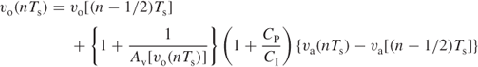
in which the effect of the nonlinear finite OTA DC gain is also accounted for. The former equation is solved by following the iterative procedure described in Section 3.3. Note from Figure 3.22 that the nonlinearity of the capacitor—not shown in Equation 3.24 for the sake of simplicity—is also taken into account in the behavioral model to get a more accurate value of ![]() .
.
During the integration phase the incomplete settling model is evaluated proceeding in a similar way as during the sampling phase (Section 2.4). The value of ![]() at the end of the integration phase of period
at the end of the integration phase of period ![]() is thus given by [38]
is thus given by [38]
3.25 
where ![]() (GMIEFF in Figure 3.23) stands for the effective OTA transconductance during the integration phase and
(GMIEFF in Figure 3.23) stands for the effective OTA transconductance during the integration phase and
3.26 
with ![]() being the voltage at the
being the voltage at the ![]() th input node of the
th input node of the ![]() th input SC branch,
th input SC branch, ![]() is the sampling capacitor of the
is the sampling capacitor of the ![]() th input SC branch, and
th input SC branch, and ![]() (CPRIMA in the C-code) is given by
(CPRIMA in the C-code) is given by
3.27 ![]()
After computing ![]() , the value of the opamp output node is solved in an iterative way (Figure 3.23) taking into account the effect of nonlinear OTA DC gain and capacitor nonlinearity. This iterative procedure converges typically in a few iterations and provides very accurate results in close agreement with transistor-level simulations [5].
, the value of the opamp output node is solved in an iterative way (Figure 3.23) taking into account the effect of nonlinear OTA DC gain and capacitor nonlinearity. This iterative procedure converges typically in a few iterations and provides very accurate results in close agreement with transistor-level simulations [5].
Before concluding this section, it is very important to pay attention to a practical issue related to the implementation of the incomplete settling error model in a programming platform in general, and in the MATLAB/SIMULINK environment in particular. It can be noted that in order to implement this error, it is not sufficient to provide information about the building block itself (i.e., the SC integrator to be modeled), but also about those building blocks connected to its output. For instance, the values of ![]() at
at ![]() are needed to compute
are needed to compute ![]() at
at ![]() —see Equation 3.23. Therefore, an accurate behavioral model must incorporate the required data computed in previous clock cycles that correspond to those building blocks connected at the output of the integrator. This can be implemented in the SIMULINK environment by using the From and Goto blocks provided by the Signal Routing SIMULINK library [29].
—see Equation 3.23. Therefore, an accurate behavioral model must incorporate the required data computed in previous clock cycles that correspond to those building blocks connected at the output of the integrator. This can be implemented in the SIMULINK environment by using the From and Goto blocks provided by the Signal Routing SIMULINK library [29].
Figure 3.27 illustrates the use of From and Goto blocks for the behavioral model of SC FE integrators in SIMULINK. In this example, two SC FE integrators are connected to build a second-order ![]() M. In order to distinguish both building blocks in their corresponding behavioral models, two different identifiers are used, named int3 and int4 in this case. As shown in the corresponding S-function diagram, From and Goto blocks allow passing of the required information between both SC integrators without actually connecting them, what notably simplifies the implementation of arbitrary
M. In order to distinguish both building blocks in their corresponding behavioral models, two different identifiers are used, named int3 and int4 in this case. As shown in the corresponding S-function diagram, From and Goto blocks allow passing of the required information between both SC integrators without actually connecting them, what notably simplifies the implementation of arbitrary ![]() Ms without modifying the model code.
Ms without modifying the model code.
Figure 3.27 Illustrating the use of From and Goto SIMULINK blocks to transmit information between the models of two SC FE integrators in a second-order ![]() M.
M.

In the example of Figure 3.27, the information provided by the back-end integrator (identified as int4) is included in the model of the front-end integrator (int3) by connecting the From block to an input port of the front-end integrator. Similarly, the front-end integrator uses the Goto block to provide its stored data to another building block. The information stored essentially consists of a data array that contains the values of the sampling capacitors and the sampled voltages of the input SC branches of a given integrator. This data is read by the model by using dynamically sized inputs, for instance uPtrs4 array in the C-code of Figure 3.21.
3.4.2 Modeling of CT Integrators using S-Functions
CT integrators constitute the most critical building blocks of CT-![]() Ms. As discussed in Chapter 2, these blocks can be implemented using different circuit topologies, namely active-RC, Gm-C, MOSFET-RC, Gm-MC, etc. All of them may have the same ideal characteristics, although involving a number of design trade-offs and error limitations that can be modeled using C-MEX S-functions. This section focuses on the behavioral modeling of S-functions for Gm-C circuits, considering their most important limiting factors. The behavioral model of other CT integrator topologies is considered in Appendices A and B.
Ms. As discussed in Chapter 2, these blocks can be implemented using different circuit topologies, namely active-RC, Gm-C, MOSFET-RC, Gm-MC, etc. All of them may have the same ideal characteristics, although involving a number of design trade-offs and error limitations that can be modeled using C-MEX S-functions. This section focuses on the behavioral modeling of S-functions for Gm-C circuits, considering their most important limiting factors. The behavioral model of other CT integrator topologies is considered in Appendices A and B.
Let us consider the Gm-C integrator conceptually depicted in Figure 3.5b, whose ideal behavior is governed by Equation 3.2. In practice, this ideal behavior is degraded by the action of a number of circuit errors, namely, input-referred thermal noise, circuit–element tolerances and mismatch, input and output voltage saturation, transconductance nonlinearity, finite OTA DC gain, transient response (including either a single-pole or a two-pole model for the OTA), etc. [39]. There are several ways of modeling these effects using S-functions, as discussed below.
Single-Pole Gm-C Model
Figure 3.28 shows the equivalent circuit of a Gm-C integrator considering a single-pole dynamic. The model includes also the following nonideal effects: input-referred thermal noise, input/output voltage saturation, time-constant error, finite DC gain (modeled as a finite output conductance), and a nonlinear transconductance that depends on the input voltage ![]() as
as
3.28 ![]()
where ![]() is the nominal value of the transconductance and
is the nominal value of the transconductance and ![]() are the nonlinear transconductance coefficients.
are the nonlinear transconductance coefficients.
Figure 3.28 Equivalent circuit of a Gm-C integrator considering a single-pole model.

The circuit errors of Figure 3.28 are computed by following the iterative procedure depicted in the flowchart of Figure 3.29. This computational model can be included in a C-MEX S-function as shown in Figure 3.30 and implemented in an S-function block as illustrated in Figure 3.31. Note that the C-MEX S-function file is made up of the same parts as those S-functions described in previous sections, beginning with a model parameter and state variable initialization and computing the different errors according to the flow of Figure 3.29. The main difference is related to those model aspects related to the timing. Thus, the CT nature of the circuit is specified in the mdInitializeSampleTimes structure, where the sample time is defined as CONTINUOUS_SAMPLE_TIME to point out that this S-function corresponds to a CT building block [34].
Figure 3.29 Flowchart of the Gm-C integrator computational model.

Figure 3.30 C-coded S-function file of a Gm-C integrator with a single-pole dynamic.

Figure 3.31 Illustrating the incorporation of the Gm-C integrator S-function in SIMULINK.

The output voltage is computed using the mdlDerivatives routine [34] that solves the following differential equation:
3.29 ![]()
where ![]() is the finite output conductance (denoted as go in Figure 3.30),
is the finite output conductance (denoted as go in Figure 3.30), ![]() is the parasitic capacitance that models the integration time-constant error (Cp in Figure 3.30), and
is the parasitic capacitance that models the integration time-constant error (Cp in Figure 3.30), and ![]() is the current-mode input that can be used for modeling the current provided by a feedback current-steering DAC in a CT-
is the current-mode input that can be used for modeling the current provided by a feedback current-steering DAC in a CT-![]() M (Figure 3.31).
M (Figure 3.31).
Two-Pole Dynamics Model
A two-pole transient response can be included in the model of a Gm-C integrator using the equivalent circuit shown in Figure 3.32. This model can be incorporated in an S-function as illustrated in Figure 3.33, which shows only the excerpt of the C-MEX file corresponding to the mdlDerivatives routine. In this case, the output voltage is computed by solving the following set of differential equations:
3.30 
Figure 3.32 Equivalent circuit of a Gm-C integrator considering a two-pole model [5].

Figure 3.33 Excerpt of the S-function of a Gm-C integrator considering a two-pole model.

where ![]() and
and ![]() are represented in Figure 3.33 by two state variables named x[0] and x[1], respectively.
are represented in Figure 3.33 by two state variables named x[0] and x[1], respectively.
Modeling Transconductors as S-Functions
The model of a Gm-C integrator can be also implemented as the cascade of two building blocks, as illustrated in Figure 3.34a: a transconductor and an output impedance circuit made up of the parallel connection of an output resistance (![]() ), the integration capacitor
), the integration capacitor ![]() , and its parasitic capacitance
, and its parasitic capacitance ![]() . Figure 3.34b shows the implementation of Figure 3.34a in SIMULINK. The transconductor S-function block includes the input-referred noise, saturation voltage at both the input and the output nodes, and a transconductance that is a nonlinear function of the input voltage given by
. Figure 3.34b shows the implementation of Figure 3.34a in SIMULINK. The transconductor S-function block includes the input-referred noise, saturation voltage at both the input and the output nodes, and a transconductance that is a nonlinear function of the input voltage given by
3.31 ![]()
where ![]() is the input-referred third-order intercept point, used as a model parameter.
is the input-referred third-order intercept point, used as a model parameter.
Figure 3.34 Gm-C integrator implemented as a transconductor and an output impedance circuit: (a) conceptual schematic and (b) implementation in SIMULINK.
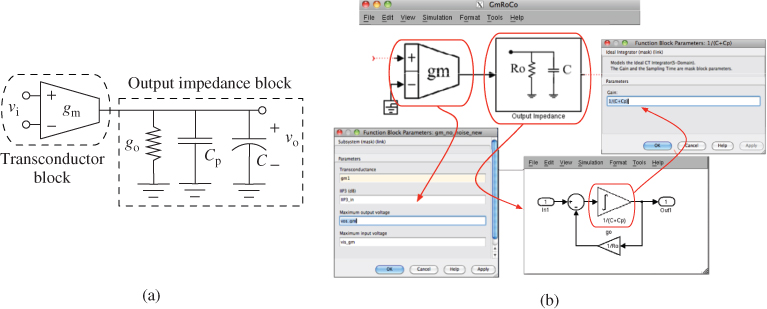
3.4.3 Behavioral Modeling of Quantizers using S-Functions
Quantizers are also essential building blocks of ![]() Ms. These blocks are made up of an ADC and a DAC that are embedded in the
Ms. These blocks are made up of an ADC and a DAC that are embedded in the ![]() M loop, the former in the feed-forward path and the latter in the feedback path.14 As it also happens with integrators, there are plenty of different ADC and DAC topologies that are usually embedded in
M loop, the former in the feed-forward path and the latter in the feedback path.14 As it also happens with integrators, there are plenty of different ADC and DAC topologies that are usually embedded in ![]() Ms. Their selection depends on many factors, such as the circuit nature of the loop filter, the number of bits (or levels) of the quantization process, the circuit topology, etc. All of them can be modeled with S-functions, following the same philosophy used for integrators. In this section, two commonly used exemplary blocks are presented as a matter of illustration. Other models of embedded ADCs and DACs can be found in Appendix B.
Ms. Their selection depends on many factors, such as the circuit nature of the loop filter, the number of bits (or levels) of the quantization process, the circuit topology, etc. All of them can be modeled with S-functions, following the same philosophy used for integrators. In this section, two commonly used exemplary blocks are presented as a matter of illustration. Other models of embedded ADCs and DACs can be found in Appendix B.
Modeling Multilevel ADCs as S-Functions
As stated in previous chapters, the quantizers embedded in ![]() Ms are usually implemented by multibit flash ADCs. These circuits—made up of a bank of comparators (or single-bit quantizers) and a resistive ladder—are subject to a number of circuit errors whose effects on the
Ms are usually implemented by multibit flash ADCs. These circuits—made up of a bank of comparators (or single-bit quantizers) and a resistive ladder—are subject to a number of circuit errors whose effects on the ![]() M performance are greatly attenuated by the action of the modulator loop filter. However, they must be taken into account in the behavioral models in order to get efficient and accurate designs. Some of these errors are comparator offset and hysteresis, integral nonlinearity (INL), gain error, etc., which can be easily modeled using S-functions following the methodology described in this section.
M performance are greatly attenuated by the action of the modulator loop filter. However, they must be taken into account in the behavioral models in order to get efficient and accurate designs. Some of these errors are comparator offset and hysteresis, integral nonlinearity (INL), gain error, etc., which can be easily modeled using S-functions following the methodology described in this section.
Figure 3.35a shows the main parts of the S-function block used for modeling a multilevel ADC. This block can be used in either DT- or CT-![]() Ms for implementing quantizers with an arbitrary number of quantization levels. This way, if an odd number of levels is set up, a midtreat quantization characteristic is implemented. Otherwise, a midrise quantizer is computed. The model includes the following circuit nonideal effects: INL, gain error, and offset error—all of them expressed in terms of the least significant bit (LSB). Other model parameters are the input and output full-scale (FS) range, the clock phase at which the input is sampled, and the sampling time.
Ms for implementing quantizers with an arbitrary number of quantization levels. This way, if an odd number of levels is set up, a midtreat quantization characteristic is implemented. Otherwise, a midrise quantizer is computed. The model includes the following circuit nonideal effects: INL, gain error, and offset error—all of them expressed in terms of the least significant bit (LSB). Other model parameters are the input and output full-scale (FS) range, the clock phase at which the input is sampled, and the sampling time.
Figure 3.35 Illustrating the behavioral model of multilevel ADCs: (a) S-function block and (b) excerpt of the C-code.

Figure 3.35b shows the main parts of the S-function file implementing the model of the multilevel ADC, whose conceptual block diagram is shown in Figure 3.36a. This model is based on the one presented in [12], which has been adapted to multilevel quantizers. Essentially, the model consists of the cascade connection of an adder block (that includes the offset error), a linear gain block, a nonlinear transfer function, and an ideal multilevel ADC. The operations of these blocks are sequentially computed in Figure 3.35b that basically codifies the following equations:
3.32 
where ![]() is the number of levels (named n_levels in Figure 3.35b),
is the number of levels (named n_levels in Figure 3.35b), ![]() is the quantization step (Xlsb in Figure 3.35b), and
is the quantization step (Xlsb in Figure 3.35b), and ![]() is the quantizer offset (off in Figure 3.35b).
is the quantizer offset (off in Figure 3.35b).
Figure 3.36 Conceptual block diagram of the behavioral model used for the quantizer embedded in ![]() Ms [12]: (a) ADC and (b) DAC.
Ms [12]: (a) ADC and (b) DAC.

Modeling Multilevel DACs as S-Functions
Embedded feedback DACs must be accurately modeled at the system level in order to take into account, from the very beginning of the design, some circuit errors that can severely degrade the performance of ![]() Ms. This is the case of multibit (or multilevel) DACs, where the mismatches among the unit circuit elements (capacitors, resistors, current sources, etc.) used for reconstructing the analog feedback signal give rise to a nonlinear input–output characteristics, and consequently to harmonic distortion. This problem is aggravated in CT-
Ms. This is the case of multibit (or multilevel) DACs, where the mismatches among the unit circuit elements (capacitors, resistors, current sources, etc.) used for reconstructing the analog feedback signal give rise to a nonlinear input–output characteristics, and consequently to harmonic distortion. This problem is aggravated in CT-![]() Ms where the feedback DAC transforms the modulator output signal from DT domain to CT domain. This signal reconstruction is very critical and subject to some limiting errors, such as clock jitter error and transient response delay, that have a significant impact on the overall behavior of
Ms where the feedback DAC transforms the modulator output signal from DT domain to CT domain. This signal reconstruction is very critical and subject to some limiting errors, such as clock jitter error and transient response delay, that have a significant impact on the overall behavior of ![]() Ms, as discussed in Chapter 2. Therefore, all these effects must be considered in the behavioral models and can be also implemented in MATLAB S-functions.
Ms, as discussed in Chapter 2. Therefore, all these effects must be considered in the behavioral models and can be also implemented in MATLAB S-functions.
As an example, Figure 3.37a shows the S-function of a multibit DAC used in CT-![]() Ms. This model allows implementation of three of the most used DAC waveforms—NRZ, RZ, and HRZ—and includes most critical errors, such as gain error, offset, INL, transient response delay, and clock jitter.
Ms. This model allows implementation of three of the most used DAC waveforms—NRZ, RZ, and HRZ—and includes most critical errors, such as gain error, offset, INL, transient response delay, and clock jitter.
Figure 3.37 Illustrating the behavioral model of multibit DACs: (a) S-function block and (b) excerpts of the C-code including the model of DAC transient response delay, clock jitter, and waveform selection.

Figure 3.37b shows the C-code of the S-function, highlighting their main parts. Basically, the behavioral model is based on the same concept used for multilevel ADCs, but implemented in a dual way as depicted in Figure 3.36b; that is, starting from an ideal D/A conversion and then applying the effects of the nonlinearity, gain error, and offset. Note that the DAC model uses the number of bits as a model parameter instead of number of levels, although the latter can be also included in the models as shown in Appendix B.
Two different cases have been considered for the DAC delay (named delay in Figure 3.37b): a fixed delay, which is independent of the input voltage, and a signal-dependent delay, which is modeled as [40]
3.33 ![]()
where ![]() stands for the fixed delay (d0 in Figure 3.37b) and
stands for the fixed delay (d0 in Figure 3.37b) and ![]() and
and ![]() (d1,x1 in Figure 3.37b are curve-fitting parameters that can either be extracted from electrical (transistor-level) simulations or be used for high-level synthesis purposes.
(d1,x1 in Figure 3.37b are curve-fitting parameters that can either be extracted from electrical (transistor-level) simulations or be used for high-level synthesis purposes.
Another important error considered in Figure 3.37 is the clock jitter. This error is modeled as a sampling time instant uncertainty given by
where ![]() ;
; ![]() is the time instant;
is the time instant; ![]() stands for the time uncertainty implemented in the model as random Gaussian noise source with zero mean and standard deviation provided as a model parameter in Figure 3.37a. This noise source is incorporated as an input port to the S-function block and included in the C-code using *uPtrs2[0] as shown in Figure 3.37b.
stands for the time uncertainty implemented in the model as random Gaussian noise source with zero mean and standard deviation provided as a model parameter in Figure 3.37a. This noise source is incorporated as an input port to the S-function block and included in the C-code using *uPtrs2[0] as shown in Figure 3.37b.
Note that the C-code modeling the clock jitter strongly depends on the DAC waveform as a different number of clock-signal edges may occur. For that reason, Equation 3.34 is valid for NRZ DAC, while the time uncertainty in the clock edges in RZ or HRZ DACs is modeled as
3.35 
where ![]() and
and ![]() refer to the time instants of the first and second clock edge, respectively, and
refer to the time instants of the first and second clock edge, respectively, and ![]() and
and ![]() stand for the corresponding clock-edge time uncertainties. Note that a variable sampled time is used in Figure 3.37b (modeled by VARIABLE_SAMPLE_TIME parameter) to take into account the effect of clock jitter on the sampling time instant.
stand for the corresponding clock-edge time uncertainties. Note that a variable sampled time is used in Figure 3.37b (modeled by VARIABLE_SAMPLE_TIME parameter) to take into account the effect of clock jitter on the sampling time instant.
3.5 SIMSIDES: A SIMULINK-Based Behavioral Simulator for  Ms
Ms
All ![]() M building blocks and their associated error mechanisms can be modeled as C-MEX S-functions following the methodology described in previous sections. On the basis of this philosophy, a complete toolbox can be developed in the MATLAB/SIMULINK environment for the time-domain behavioral simulation of
M building blocks and their associated error mechanisms can be modeled as C-MEX S-functions following the methodology described in previous sections. On the basis of this philosophy, a complete toolbox can be developed in the MATLAB/SIMULINK environment for the time-domain behavioral simulation of ![]() Ms. This is the case of SIMSIDES, a SIMulink-based SIgma-DElta simulator that takes advantage of the benefits provided by MATLAB, namely, a friendly user interface, high flexibility for the extension of new models and building blocks, and a powerful set of signal processing routines [5].
Ms. This is the case of SIMSIDES, a SIMulink-based SIgma-DElta simulator that takes advantage of the benefits provided by MATLAB, namely, a friendly user interface, high flexibility for the extension of new models and building blocks, and a powerful set of signal processing routines [5].
SIMSIDES can be used for simulating any arbitrary ![]() M topology, considering a circuit implementation with either DT circuits, CT circuits, or a mix of them, that is, the so-called hybrid CT/DT-
M topology, considering a circuit implementation with either DT circuits, CT circuits, or a mix of them, that is, the so-called hybrid CT/DT-![]() Ms. In the case of DT-
Ms. In the case of DT-![]() Ms, behavioral models included in SIMSIDES consider either SC or SI [41] circuit techniques, although the majority of models in SIMSIDES deal with SC circuits, because is the most commonly used DT circuit technique. As far as CT-
Ms, behavioral models included in SIMSIDES consider either SC or SI [41] circuit techniques, although the majority of models in SIMSIDES deal with SC circuits, because is the most commonly used DT circuit technique. As far as CT-![]() Ms is concerned, the main integrator circuit topologies are included in SIMSIDES S-functions, namely: Gm-C, active-RC, Gm-MC, etc. Overall, more than 150 S-functions and 250 behavioral models are available in the toolbox. A list of the most important ones is included in Appendix B, where a brief description of the different models, their main functionality, and parameters is given. This section summarizes the most important features of SIMSIDES, overviewing its model libraries, its general structure, and the user interface.
Ms is concerned, the main integrator circuit topologies are included in SIMSIDES S-functions, namely: Gm-C, active-RC, Gm-MC, etc. Overall, more than 150 S-functions and 250 behavioral models are available in the toolbox. A list of the most important ones is included in Appendix B, where a brief description of the different models, their main functionality, and parameters is given. This section summarizes the most important features of SIMSIDES, overviewing its model libraries, its general structure, and the user interface.
3.5.1 Model Libraries Included in SIMSIDES
The building blocks modeled in SIMSIDES are grouped into a number of SIMULINK libraries and sublibraries which can be classified attending to different criteria, as conceptually depicted in Figure 3.38. The first classification criterion is related to the modulator system hierarchy level in which a given building block is placed. Attending to this criterion, ![]() M building blocks are organized in the following libraries: integrators and resonators (basic blocks in
M building blocks are organized in the following libraries: integrators and resonators (basic blocks in ![]() Ms), quantizers, DACs, and auxiliary blocks. The latter include analog and digital mixers, DEM algorithm S-functions, latches models, etc, which are required to simulate some specific
Ms), quantizers, DACs, and auxiliary blocks. The latter include analog and digital mixers, DEM algorithm S-functions, latches models, etc, which are required to simulate some specific ![]() M architectures. A second classification criterion deals with the circuit technique used for implementing
M architectures. A second classification criterion deals with the circuit technique used for implementing ![]() M building blocks. Thus, there are sublibraries including FE and LD integrators, Gm-C and active-RC integrators, etc.
M building blocks. Thus, there are sublibraries including FE and LD integrators, Gm-C and active-RC integrators, etc.
Figure 3.38 Classification of SIMSIDES model libraries.

All SIMSIDES model libraries are in turn classified into two main categories (not shown in Figure 3.38 for the sake of simplicity): ideal libraries and real libraries. The former ones include only S-functions that contain ideal models of different building blocks—classified attending to the aforementioned criteria. By contrast, real libraries contain S-function behavioral models that include the most critical error mechanisms that degrade the performance of ![]() Ms. Table 3.2 summarizes all building blocks modeled in SIMSIDES as well as the error mechanisms included in their S-function behavioral models.
Ms. Table 3.2 summarizes all building blocks modeled in SIMSIDES as well as the error mechanisms included in their S-function behavioral models.
Table 3.2 Circuits and error mechanisms modeled in SIMSIDES
| Circuit Technique | Building Block | Error Mechanism |
| Switched-Capacitor | Amplifiers | Finite and Nonlinear DC gain, incomplete settling error, output swing limitation, thermal noise |
| Switches | Thermal noise, finite and nonlinear switch on-resistance | |
| Capacitors | Mismatch, nonlinearities, parasitic capacitances | |
| Switched-Current | Memory cells and Integrators | Linear and nonlinear gain error, thermal noise, finite output–input conductance ratio error, charge injection error, incomplete settling error |
| Continuous-Time | Integrators | Finite and nonlinear DC gain, nonlinear transconductance, thermal noise, output swing limitation, transient response |
| All circuit techniques | Clock generator | Clock jitter |
| Comparators | Hysteresis and offset | |
| Quantizers/DACs | Nonlinearity (INL), gain error, excess loop delay, offset |
As an illustration, Figure 3.39 shows some of the most representative libraries and sublibraries including integrators, resonators, quantizers, and DACs. As illustrated in Figure 3.40, there is a number of different SC integrator S-function blocks with different number of input branches and nonideal effects included in their models, going from ideal models to the most precise ones that include all circuit nonidealities. The benefits of this approach are twofold: On the one hand, it allows to evaluate the impact of isolated circuit error mechanisms in a very simple way, without dealing with model parameters. This is particularly appropriate for the high-level sizing process where different error parameters are taken as design variables. On the other hand, the use of different building-block model approaches, which evolve from the most ideal and simplest approximations to the most accurate and complex ones, may be particularly useful for novel designers, who are not very familiar with some circuit-level parameters used in the most precise behavioral models.
Figure 3.39 Illustrating some SIMSIDES model libraries.

Figure 3.40 SIMSIDES library including different SC FE integrator model approaches.
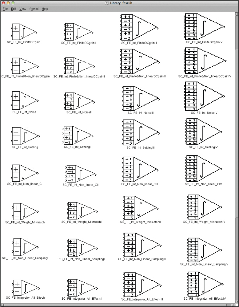
Apart from the mentioned libraries containing isolated ![]() M building blocks, SIMSIDES includes also some additional libraries with examples of the most commonly used
M building blocks, SIMSIDES includes also some additional libraries with examples of the most commonly used ![]() M architectures, considering both LP and BP topologies, single-loop and cascade, single-bit and multibit embedded quantization, different circuit techniques (DT, CT, and hybrid CT/DT), etc.
M architectures, considering both LP and BP topologies, single-loop and cascade, single-bit and multibit embedded quantization, different circuit techniques (DT, CT, and hybrid CT/DT), etc.
3.5.2 Structure of SIMSIDES and User Interface
Figure 3.41 shows the general structure of SIMSIDES. First, the modulator architecture is defined by properly interconnecting the building blocks included in the SIMSIDES libraries discussed in the previous section. After the modulator block diagram has been created, the designer can set the model parameters and the simulation options required by the toolbox to do the simulation. Most commonly used analyses can be carried out, namely, time-domain simulations to obtain output spectra and SNR/SNDR-versus-input curves, parametric simulations considering the variation of a given model parameter, Monte Carlo simulations, etc. Output data generated by the simulator consists of time-domain series which can be further processed to get typical performance figures. This way, both integrator input/output histograms and/or output spectra are computed using the routines provided by the signal processing toolbox in MATLAB [28]. Other typical performance metrics can be evaluated, such as SNR/SNDR, harmonic and intermodulation distortion, etc. These figures are computed using a collection of internal MATLAB routines, specifically developed for SIMSIDES [5].
Figure 3.41 General structure of SIMSIDES.
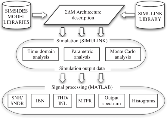
SIMSIDES includes a graphical user interface (GUI) that allows designers to browse through all steps of the simulation and to postprocess the simulation results. As an illustration, Figure 3.42 shows some of the most important parts of the SIMSIDES GUI, highlighting some of its menus. Although a more detailed explanation about SIMSIDES GUI is given in Appendix A, the use of the toolbox is illustrated in this section through a simple example based on the behavioral model of a cascade 2-1 SC-![]() M, where several types of analyses are carried out.
M, where several types of analyses are carried out.
Figure 3.42 Illustrating some parts of the SIMSIDES GUI.
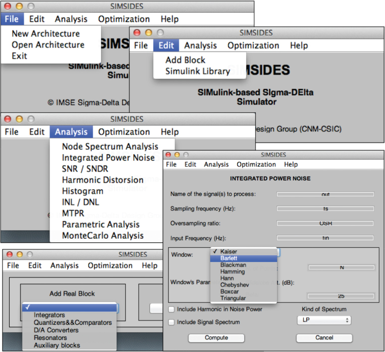
Creating a New  M Block Diagram
SIMSIDES is started by typing simsides in the MATLAB command window and the main window is displayed. Selecting the pop-up menu named File and then New Architecture (Figure 3.42), a new (empty) SIMULINK model window is displayed. This is illustrated in Figure 3.43 for a cascade 2-1 SC topology that can be created by adding building blocks from Edit->Add Block pop-up menu and then choosing the circuit technique to implement the integrator blocks—SC FE integrators in this case. The corresponding model library—named fesclib in this example (illustrated in Figure 3.40)—is displayed and the appropriate integrator blocks can be included in the new model by dragging and dropping the corresponding blocks. A similar procedure can be followed to incorporate the comparator model and, once all blocks are properly connected, the block diagram in Figure 3.43 is finished.
Figure 3.43 Creating the block diagram of a cascade 2-1 SC-![]() M in SIMSIDES.
M in SIMSIDES.

Setting Model Parameters
Once the block diagram has been defined, the next step consists of setting the model parameters. Although this is something that can be done in the MATLAB command window, as the number of model parameters increases, it becomes more practical to save their values in an M-file. In addition to the model parameters themselves, some global parameters must be defined in order to run the simulation. These parameters are input signal frequency (fi in Figure 3.43), sampling time and frequency (Ts,fs), and the number of simulation clock cycles (N=65536). The latter must be included in the Configuration Parameters menu of the SIMULINK model window where the solver options is also configured (Fixed-step and discrete in this example).
Simulation Analyses
After setting the model parameters, a simulation can be started from the Simulation->Start pop-up menu as is usually done in SIMULINK. This is the usual procedure followed in SIMSIDES to run a one-sample simulation that is used for computing an output spectrum, for instance. Thus, once the simulation has finished, the output spectrum can be computed and plotted from the Analysis->Node Spectrum Analysis pop-up menu (Figure 3.42). Selecting this option, a new window is displayed to set some parameters required to compute the output spectrum, such as the sampling frequency, the signal to be processed, as well as some parameters related to the window used for FFT computation. In the example shown in Figure 3.44a, a Kaiser window with N points and a beta of ![]() has been used. As an illustration, Figure 3.44b shows the in-band output spectrum of the modulator in Figure 3.43. This figure plots also the IBN corresponding to
has been used. As an illustration, Figure 3.44b shows the in-band output spectrum of the modulator in Figure 3.43. This figure plots also the IBN corresponding to ![]() . This data has been obtained by choosing Analysis->Integrated Power Noise pop-up menu. In a similar way, the SNR/SNDR can be computed by selecting Analysis->Integrated Power Noise in the SIMSIDES main window.
. This data has been obtained by choosing Analysis->Integrated Power Noise pop-up menu. In a similar way, the SNR/SNDR can be computed by selecting Analysis->Integrated Power Noise in the SIMSIDES main window.
Figure 3.44 Computing IBN in SIMSIDES: (a) user window and (b) in-band output spectrum.

Apart from the mentioned simulation analyses, other useful performance metrics can also be evaluated in SIMSIDES, such as linearity—considering either static figures such as INL or dynamic figures such as THD or MTPR. All these analyses can be combined with a parametric analysis in order to evaluate the impact of a given model parameter. This kind of analysis is especially useful for high-level sizing, as will be illustrated in the next section. Here, an example of this analysis is shown to obtain a typical SNR-versus-input figure.
To this purpose, Analysis->Parametric Analysis pop-up menu is chosen and a new window is displayed as shown in Figure 3.45a. There is the possibility to select between one-parameter analysis or two-parameter analysis. In this example, the former case is chosen and the input signal amplitude range is defined. After that, the next steps consist of defining several parameters required to compute the SNDR. Once all parameters have been properly defined, the parametric simulation is started. A simulation-progress window is graphically displayed and finally the results are plotted in Figure 3.45b.
Figure 3.45 Computing SNDR versus input amplitude in SIMSIDES: (a) user window and (b) SNDR versus input amplitude.

3.6 Using SIMSIDES for the High-Level Sizing and Verification of  Ms
Ms
To conclude this chapter, this section illustrates the use of SIMSIDES for the high-level sizing and verification of ![]() Ms. To this purpose, two different
Ms. To this purpose, two different ![]() M architectures and circuit techniques are considered as case studies:
M architectures and circuit techniques are considered as case studies:
- An SC second-order single-loop single-bit
 M
M - A CT fifth-order cascade 3-2 multibit
 M
M
3.6.1 SC Second-Order Single-Bit  M
M
Let us consider the ![]() -domain block diagram of a second-order
-domain block diagram of a second-order ![]() M shown in Figure 3.46a. In this example, an ideal feedback DAC and a one-bit quantization with 1-V FS range will be assumed. This block diagram can be implemented in SIMSIDES as shown in Figure 3.46b, where
M shown in Figure 3.46a. In this example, an ideal feedback DAC and a one-bit quantization with 1-V FS range will be assumed. This block diagram can be implemented in SIMSIDES as shown in Figure 3.46b, where ![]() -domain transfer functions have been replaced by SC FE integrator S-function blocks as illustrated in Figure 3.46c.
-domain transfer functions have been replaced by SC FE integrator S-function blocks as illustrated in Figure 3.46c.
Figure 3.46 Second-order SC-![]() M case study: (a)
M case study: (a) ![]() -domain block diagram, (b) SIMSIDES implementation, and (c) symbol of a two-branch SC integrator in SIMSIDES and its equivalent circuit.
-domain block diagram, (b) SIMSIDES implementation, and (c) symbol of a two-branch SC integrator in SIMSIDES and its equivalent circuit.

Figure 3.47 represents the ideal modulator output spectrum and the IBN for ![]() , considering a sampling frequency of
, considering a sampling frequency of ![]() MHz and an input tone with half-scale amplitude (0.5 V). The shaped quantization noise increases at a rate of 15 dB/octave—according to theoretical predictions. The ideal SNR computed by SIMSIDES is 87 dB (
MHz and an input tone with half-scale amplitude (0.5 V). The shaped quantization noise increases at a rate of 15 dB/octave—according to theoretical predictions. The ideal SNR computed by SIMSIDES is 87 dB (![]() bit), 103 dB (
bit), 103 dB (![]() bit), and 119 dB (
bit), and 119 dB (![]() bit), respectively, for
bit), respectively, for ![]() , corresponding to a signal bandwidth of
, corresponding to a signal bandwidth of ![]() 10, 5, and 2.5 kHz, respectively. Alternatively, the same ideal effective resolutions can be obtained for a signal bandwidth of
10, 5, and 2.5 kHz, respectively. Alternatively, the same ideal effective resolutions can be obtained for a signal bandwidth of ![]() kHz if
kHz if ![]() 2.56, 5.12, and 10.24 MHz. In practice, this ideal performance is degraded by the action of circuit errors. In this example, the impact of the following nonidealities will be evaluated: opamp finite DC gain, thermal noise, and incomplete transient response. For each nonideality, the error bound that allows achieving the ideal effective resolution will be found in order to map modulator-level specifications onto building-block specifications.
2.56, 5.12, and 10.24 MHz. In practice, this ideal performance is degraded by the action of circuit errors. In this example, the impact of the following nonidealities will be evaluated: opamp finite DC gain, thermal noise, and incomplete transient response. For each nonideality, the error bound that allows achieving the ideal effective resolution will be found in order to map modulator-level specifications onto building-block specifications.
Figure 3.47 (a) Ideal output spectrum of the modulator in Figure 3.46 and (b) IBN for ![]() .
.
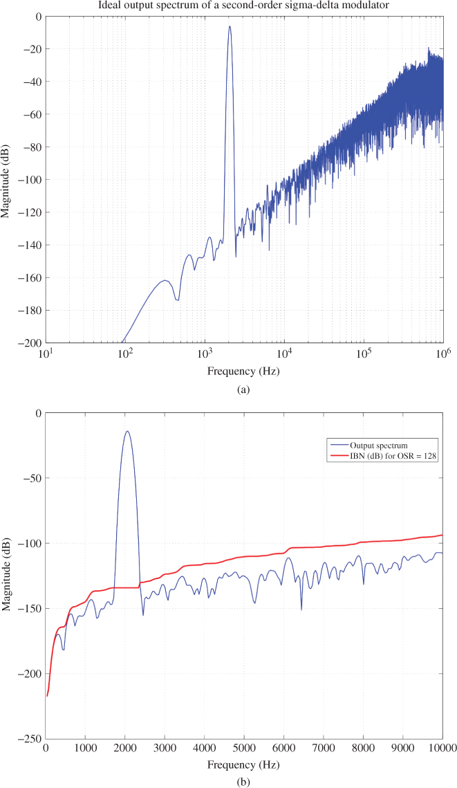
Effect of Amplifier Finite DC Gain
There are two possibilities to analyze the effect of a given error in SIMSIDES. One consists of using the behavioral model that contains only that isolated effect, whereas the other consists of using a complete behavioral model in which all error parameters are set ideal except for those related to the nonideality which is going to be evaluated. In this example, the first approach will be followed. Thus, in order to simulate the effect of finite DC gain ![]() the corresponding S-function models of SC FE integrators available in SIMSIDES are used.
the corresponding S-function models of SC FE integrators available in SIMSIDES are used.
A parametric analysis can be carried out in SIMSIDES in order to obtain the minimum (or critical) value of ![]() —represented by
—represented by ![]() —required to achieve the ideal resolution. This is illustrated in Figure 3.48 where the SNDR is plotted versus
—required to achieve the ideal resolution. This is illustrated in Figure 3.48 where the SNDR is plotted versus ![]() for
for ![]() , 256, and 512, resulting in
, 256, and 512, resulting in ![]() , and
, and ![]() , respectively.15
, respectively.15
Figure 3.48 SNDR versus ![]() of the
of the ![]() M in Figure 3.46 for different values of OSR.
M in Figure 3.46 for different values of OSR.

Effect of Thermal Noise
Following the same procedure as in the previous section, the effect of circuit (thermal) noise can be simulated. Two main thermal noise sources are considered, namely, the input-referred noise of the opamp (denoted as ![]() ) and the
) and the ![]() noise—evaluated by varying the value of the sampling capacitance
noise—evaluated by varying the value of the sampling capacitance ![]() . In this example, only the contribution of the front-end integrator will be taken into account.16
. In this example, only the contribution of the front-end integrator will be taken into account.16
Figure 3.49 depicts SNR versus ![]() and
and ![]() for
for ![]() 128, 256, and 512. According to Equation 3.14, ideal values for other model parameters except
128, 256, and 512. According to Equation 3.14, ideal values for other model parameters except ![]() and
and ![]() are considered. Note from Figure 3.49 that a critical value of
are considered. Note from Figure 3.49 that a critical value of ![]() can be tolerated in all cases while
can be tolerated in all cases while ![]() and
and ![]() pF is approximately required for
pF is approximately required for ![]() 128, 256, and 512, respectively. Note that such large values required for
128, 256, and 512, respectively. Note that such large values required for ![]() are a direct consequence of the high effective resolutions with low modulator filter order and single-bit embedded quantizer. These capacitor values may force reducing the digitized signal bandwidth
are a direct consequence of the high effective resolutions with low modulator filter order and single-bit embedded quantizer. These capacitor values may force reducing the digitized signal bandwidth ![]() in order to reduce the impact of incomplete settling with a feasible power consumption.
in order to reduce the impact of incomplete settling with a feasible power consumption.
Figure 3.49 Effect of thermal noise sources on the ![]() M in Figure 3.46: (a) SNR versus
M in Figure 3.46: (a) SNR versus ![]() and (b) SNR versus
and (b) SNR versus ![]() .
.

Effect of the Incomplete Settling Error
In order to evaluate the impact of the incomplete settling error, two model parameters are considered, namely, the OTA transconductance ![]() and the maximum OTA output current
and the maximum OTA output current ![]() . The former determines the minimum requirements in terms of GB, whereas the latter limits the maximum SR that can be achieved for a given value of the equivalent load capacitance—automatically computed by the SIMSIDES model as discussed in Section 3.4. As in previous errors, only the impact of the front-end integrator is considered here for illustration purposes.
. The former determines the minimum requirements in terms of GB, whereas the latter limits the maximum SR that can be achieved for a given value of the equivalent load capacitance—automatically computed by the SIMSIDES model as discussed in Section 3.4. As in previous errors, only the impact of the front-end integrator is considered here for illustration purposes.
Figure 3.50 shows the effect of ![]() and
and ![]() on the performance of the modulator for different values of OSR. Note that in this case the absolute value of
on the performance of the modulator for different values of OSR. Note that in this case the absolute value of ![]() and
and ![]() are important, because the incomplete setting affects the dynamic response of the integrators. In this example, an input tone at
are important, because the incomplete setting affects the dynamic response of the integrators. In this example, an input tone at ![]() is considered, for
is considered, for ![]() kHz. Figure 3.50a depicts the modulator SNDR versus
kHz. Figure 3.50a depicts the modulator SNDR versus ![]() , for
, for ![]() 10 pF and
10 pF and ![]() mA. Considering these simulation conditions, the effect of SR can be neglected. Alternatively, Figure 3.50b depicts the SNDR versus
mA. Considering these simulation conditions, the effect of SR can be neglected. Alternatively, Figure 3.50b depicts the SNDR versus ![]() considering
considering ![]() 5 mA V
5 mA V![]() , so that only the effect of SR is evaluated and the impact of GB is nulled. The critical values of
, so that only the effect of SR is evaluated and the impact of GB is nulled. The critical values of ![]() and
and ![]() for the different cases are highlighted in the figure.
for the different cases are highlighted in the figure.
Figure 3.50 Effect of incomplete settling on the ![]() M in Figure 3.46 for
M in Figure 3.46 for ![]() kHz: (a) SNDR versus
kHz: (a) SNDR versus ![]() for
for ![]() mA and (b) SNR versus
mA and (b) SNR versus ![]() for
for ![]() 5 mA V
5 mA V![]() .
.

Cumulative Effect of All Errors
Simulations carried out in previous sections analyzed the isolated impact of the most important circuit errors limiting the performance of the ![]() M shown in Figure 3.46. However, that performance can be further degraded as a consequence of the cumulative effect of the different errors acting together—which is actually the case in practical situations! To illustrate this effect, Figure 3.51 depicts the modulator SNDR versus
M shown in Figure 3.46. However, that performance can be further degraded as a consequence of the cumulative effect of the different errors acting together—which is actually the case in practical situations! To illustrate this effect, Figure 3.51 depicts the modulator SNDR versus ![]() considering both its isolated effect and the cumulative effect of this parameter, that is, considering other nonideal model parameters. Note that in the latter case, a more demanding value of
considering both its isolated effect and the cumulative effect of this parameter, that is, considering other nonideal model parameters. Note that in the latter case, a more demanding value of ![]() is required to achieve the specified resolution.
is required to achieve the specified resolution.
Figure 3.51 Illustrating the cumulative and isolated effect of the amplifier output current ![]() .
.

Figure 3.52 plots the output spectrum of the modulator considering all circuit errors, taking into account the critical values of error model parameters obtained for ![]() 512. Figure 3.53 depicts the SNDR versus input signal level for different values of OSR and
512. Figure 3.53 depicts the SNDR versus input signal level for different values of OSR and ![]() . Note that the achieved effective resolution is according to the specifications.
. Note that the achieved effective resolution is according to the specifications.
Figure 3.52 Output spectrum of the ![]() M in Figure 3.46 considering the effect of all circuit errors.
M in Figure 3.46 considering the effect of all circuit errors.

Figure 3.53 SNDR versus input signal level for ![]() kHz considering all circuit errors.
kHz considering all circuit errors.

The results of the high-level sizing process are summarized in Table 3.3, where system-level (modulator) specifications are mapped into building-block (integrator) specifications. For the sake of completeness, the required values for GB and SR are also included in the table. Note that this data takes into account the interaction of different circuit errors considered in the example and hence may be more restrictive than that obtained from the isolated analysis described. In this case, the effect of switch on-resistance on the OTA transconductance and GB described in Section 3.4.1 has not been taken into account for the sake of simplicity. However, this effect should be considered in practice, resulting in more demanding integrator dynamic specifications. As an illustration, Figure 3.54 depicts the information provided by the corresponding SIMSIDES integrator model if the mentioned degradation is considered. Among other data, the model provides the effective values of the equivalent load capacitance, GB, and SR obtained for each clock phase. Taking into account these model parameters, the half-scale SNDR for ![]() 128 is 78.3 dB, that is, approximately 9 dB less than the ideal one.
128 is 78.3 dB, that is, approximately 9 dB less than the ideal one.
Table 3.3 High-level sizing of the second-order SC-![]() M shown in Figure 3.46 (
M shown in Figure 3.46 (![]() 2.6 pF)
2.6 pF)

Figure 3.54 Information provided by the SIMSIDES SC FE integrator model when the effect of switch on-resistance is taken into account in the transient response.

3.6.2 CT Fifth-Order Cascade 3-2 Multibit  M
M
The second case study is a CT two-stage cascade ![]() M consisting of a third-order front-end stage and a second-order back-end stage. Figure 3.55a shows the conceptual block schematic of the modulator and its corresponding implementation in SIMSIDES is depicted in Figure 3.55b [42]. The front-end stage is made up of an integrator and a resonator, whereas the second-stage loop filter is essentially a resonator. Multibit (4-bit) quantization and NRZ feedback DAC are used in both stages and DEM techniques are also included to reduce the impact of DAC mismatch on the modulator linearity. In both stages an extra feedback branch—made up of a DAC and a D-latch—is connected from the output to the input of the quantizer to compensate for the effect of excess loop delay [43], as described in Section 2.10.
M consisting of a third-order front-end stage and a second-order back-end stage. Figure 3.55a shows the conceptual block schematic of the modulator and its corresponding implementation in SIMSIDES is depicted in Figure 3.55b [42]. The front-end stage is made up of an integrator and a resonator, whereas the second-stage loop filter is essentially a resonator. Multibit (4-bit) quantization and NRZ feedback DAC are used in both stages and DEM techniques are also included to reduce the impact of DAC mismatch on the modulator linearity. In both stages an extra feedback branch—made up of a DAC and a D-latch—is connected from the output to the input of the quantizer to compensate for the effect of excess loop delay [43], as described in Section 2.10.
Figure 3.55 Gm-C fifth-order cascade 3-2 ![]() M with 4-bit quantization in both stages: (a) conceptual schematic and (b) SIMSIDES implementation.
M with 4-bit quantization in both stages: (a) conceptual schematic and (b) SIMSIDES implementation.

The loop filter of both stages is implemented using Gm-C integrators, whereas current-mode DACs are used in the feedback loop. The modulator has been synthesized in the CT domain following the methodology described in [44] and resonator poles are placed at an optimum position to minimize the magnitude of NTF within the signal bandwidth. Similar to any other cascade ![]() M, the DCL functions of each stage (i.e.,
M, the DCL functions of each stage (i.e., ![]() , not explicitly shown in Figure 3.55 for the sake of simplicity) can be derived from the STF and NTF of both modulator stages, by annulling the first-stage quantization error at the overall modulator output [44] (Section 1.5).
, not explicitly shown in Figure 3.55 for the sake of simplicity) can be derived from the STF and NTF of both modulator stages, by annulling the first-stage quantization error at the overall modulator output [44] (Section 1.5).
Note from Figure 3.55b that Gm-C integrators are implemented in SIMSIDES using the model described in Section 3.4.2 (Figure 3.34), that is, as the cascade of a transconductor and an output impedance circuit (output resistance and capacitance in parallel). Alternatively, Gm-C integrators can be also modeled in SIMSIDES as a single building block as shown in Figure 3.31. This approach is more suited for those ![]() Ms with a reduced number of loop-filter coefficients—commonly implemented as transconductors. In contrast, the modulator in this example has a number of feed-forward coefficients which are commonly implemented as transconductors.
Ms with a reduced number of loop-filter coefficients—commonly implemented as transconductors. In contrast, the modulator in this example has a number of feed-forward coefficients which are commonly implemented as transconductors.
Table 3.4 sums up the values of loop-filter transconductances ![]() , as well as the capacitances
, as well as the capacitances ![]() used in the modulator. These values have been found through an iterative simulation-based process that, starting from the nominal values required to place the NTF zeros, optimizes the modulator performance in terms of DR and stability within the FS range. Unit transconductors are used in the majority of loop-filter transconductors which can be tuned to keep the time constant
used in the modulator. These values have been found through an iterative simulation-based process that, starting from the nominal values required to place the NTF zeros, optimizes the modulator performance in terms of DR and stability within the FS range. Unit transconductors are used in the majority of loop-filter transconductors which can be tuned to keep the time constant ![]() unchanged over
unchanged over ![]() variations.
variations.
Table 3.4 Loop-filter coefficients of the CT cascade 3-2 ![]() M in Figure 3.55
M in Figure 3.55
| Unit circuit elements |
| Capacitors |
| Feed-forward transconductances |
| Feedback transconductances |
Figure 3.56a shows the ideal output spectrum of the modulator considering an ![]() dBFS input tone at 1.49 MHz when clocked at
dBFS input tone at 1.49 MHz when clocked at ![]() MHz. Note that shaped quantization noise presents two notches at 11.5 and 18.5 MHz which minimize the IBN in the target signal bandwidth (
MHz. Note that shaped quantization noise presents two notches at 11.5 and 18.5 MHz which minimize the IBN in the target signal bandwidth (![]() 20 MHz). The ideal effective resolution achieved by the modulator is illustrated in Figure 3.56b that depicts the SNDR versus input signal level for
20 MHz). The ideal effective resolution achieved by the modulator is illustrated in Figure 3.56b that depicts the SNDR versus input signal level for ![]() , corresponding to
, corresponding to ![]() MHz and
MHz and ![]() MHz. Under these conditions, the maximum effective resolution that can be achieved is approximately 13 bit. However, this performance is degraded in practice by the action of circuit nonidealities, as analyzed subsequently.
MHz. Under these conditions, the maximum effective resolution that can be achieved is approximately 13 bit. However, this performance is degraded in practice by the action of circuit nonidealities, as analyzed subsequently.
Figure 3.56 Ideal simulation results of the modulator in Figure 3.55: (a) output spectrum and (b) SNDR versus input signal level for ![]() (
(![]() 20 MHz,
20 MHz, ![]() 240 MHz), considering a FS reference of 0.5 V.
240 MHz), considering a FS reference of 0.5 V.
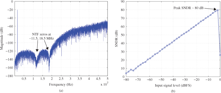
Figure 3.57 Effect of finite DC gain of loop-filter transconductors on the SNDR of Figure 3.55 for different values of OSR.

Impact of Nonideal Effects
The behavioral model used for the transconductors in SIMSIDES takes into account several nonideal circuit effects,17 including finite DC gain, output saturation voltage, and the input-referred third-order intercept point IIP3. As an illustration, Figure 3.57 shows the effect of the finite DC gain of loop-filter transconductors on the SNDR for ![]() , when clocked at
, when clocked at ![]() MHz. It can be noted that as the OSR increases, the effect of this error is attenuated, as predicted by the theoretical analysis described in Section 2.2. For a signal bandwidth of
MHz. It can be noted that as the OSR increases, the effect of this error is attenuated, as predicted by the theoretical analysis described in Section 2.2. For a signal bandwidth of ![]() MHz (
MHz (![]() ), a finite DC gain larger than 50 dB is required.
), a finite DC gain larger than 50 dB is required.
Figure 3.58 illustrates the effect of IIP3 on the modulator performance, comparing the degradation caused by different transconductors, namely, front-end transconductor (![]() in Figure 3.55), input feed-forward transconductor (
in Figure 3.55), input feed-forward transconductor (![]() ), and the rest of loop-filter transconductors. Figure 3.58a and b illustrates the output spectrum of the modulator considering two −10 dBFS input tones located at 1.49 and 2.02 MHz. The output spectrum in Figure 3.58a assumes an IIP3
), and the rest of loop-filter transconductors. Figure 3.58a and b illustrates the output spectrum of the modulator considering two −10 dBFS input tones located at 1.49 and 2.02 MHz. The output spectrum in Figure 3.58a assumes an IIP3 ![]() 20 dBm for all loop-filter transconductors and that
20 dBm for all loop-filter transconductors and that ![]() and
and ![]() are ideal. In contrast, Figure 3.58b assumes that all transconductors are ideal, except for the front-end transconductor that has an IIP3
are ideal. In contrast, Figure 3.58b assumes that all transconductors are ideal, except for the front-end transconductor that has an IIP3 ![]() 20 dBm. As expected, the front-end transconductor severely degrades the linearity of the modulator, causing a number of intermodulation products to appear in the signal band. The effect of the nonlinearity of the different transcondutors on the modulator resolution is better illustrated in Figure 3.58c that represents the SNDR versus IIP3 of the different types of transconductors in the modulator. Note that the effective resolution is not degraded if IIP3
20 dBm. As expected, the front-end transconductor severely degrades the linearity of the modulator, causing a number of intermodulation products to appear in the signal band. The effect of the nonlinearity of the different transcondutors on the modulator resolution is better illustrated in Figure 3.58c that represents the SNDR versus IIP3 of the different types of transconductors in the modulator. Note that the effective resolution is not degraded if IIP3 ![]() 28 dBm in the front-end transconductor. This specification is relaxed for the rest of transconductors, in which IIP3
28 dBm in the front-end transconductor. This specification is relaxed for the rest of transconductors, in which IIP3 ![]() 5 dBm is enough to achieve the ideal SNDR.
5 dBm is enough to achieve the ideal SNDR.
Figure 3.58 Effect of transconductance nonlinearity on the performance of the CT-![]() M in Figure 3.55: (a) output spectrum assuming that
M in Figure 3.55: (a) output spectrum assuming that ![]() and
and ![]() are ideal and that all loop-filter transconductors have an IIP3
are ideal and that all loop-filter transconductors have an IIP3 ![]() dBm, (b) output spectrum considering that all transconductors are ideal, except for
dBm, (b) output spectrum considering that all transconductors are ideal, except for ![]() that has an IIP3
that has an IIP3 ![]() dBm, and (c) SNDR versus IIP3 for the different transconductors.
dBm, and (c) SNDR versus IIP3 for the different transconductors.

Apart from the impact of the aforementioned nonidealities, the effect of circuit element tolerances and component mismatch are particularly critical in the design of cascade CT-![]() Ms. The absolute tolerances can be controlled by using time-constant tuning, as is the case for this design example. However, the impact of mismatch error still remains and must be taken into account at the early design stages. Behavioral simulation using SIMSIDES can be used for this purpose. Thus, in order to evaluate the impact of this error on the performance of the modulator in Figure 3.55, maximum values of mismatch were estimated for the 130 nm CMOS process of the final implementation. The results of this analysis are shown in Figure 3.59, where the SNR is represented as a function of the standard deviation of transconductances and capacitances (
Ms. The absolute tolerances can be controlled by using time-constant tuning, as is the case for this design example. However, the impact of mismatch error still remains and must be taken into account at the early design stages. Behavioral simulation using SIMSIDES can be used for this purpose. Thus, in order to evaluate the impact of this error on the performance of the modulator in Figure 3.55, maximum values of mismatch were estimated for the 130 nm CMOS process of the final implementation. The results of this analysis are shown in Figure 3.59, where the SNR is represented as a function of the standard deviation of transconductances and capacitances (![]() and
and ![]() , respectively). Note that for each point of this surface, a Monte Carlo analysis consisting of 150 SIMSIDES simulations was carried out. The value of SNR that is represented in this figure corresponds to that obtained by more than 90
, respectively). Note that for each point of this surface, a Monte Carlo analysis consisting of 150 SIMSIDES simulations was carried out. The value of SNR that is represented in this figure corresponds to that obtained by more than 90![]() of the simulations for each value of
of the simulations for each value of ![]() and
and ![]() . Note that even for the worst-case mismatch, an effective resolution higher than 12 bits can be achieved.
. Note that even for the worst-case mismatch, an effective resolution higher than 12 bits can be achieved.
Figure 3.59 Illustrating the effect of mismatch on the SNR of the ![]() M in Figure 3.55.
M in Figure 3.55.

High-Level Synthesis and Verification
As a case study, let us consider that the modulator in Figure 3.55 is designed to fulfill the following specifications: 12 bit effective resolution within 20-MHz signal bandwidth [44]. These specifications can be mapped onto the modulator building-block specifications by following a parametric-based analysis, as described in the previous section. Alternatively, an optimization-based procedure can be followed in which an optimization engine is used for design parameter selection and a behavioral simulator (SIMSIDES in this case) is used for performance evaluation [5]. As an illustration of the latter approach, a statistical optimizer was combined with SIMSIDES for the high-level sizing of the ![]() M in Figure 3.55.
M in Figure 3.55.
Table 3.5 sums up the results of the sizing process, showing the critical (maximum/minimum) values of the circuit electrical performance parameters that can be tolerated to meet the required modulator performance. As stated earlier, the specifications of the front-end transconductor—specifically the finite DC gain and the third-order nonlinearity—are more demanding than the rest of transconductors. For this reason, different circuit topologies are, in practice, used for implementing the front-end transconductor and the loop-filter transconductors in Gm-C ![]() Ms, as will be discussed in Chapter 4.
Ms, as will be discussed in Chapter 4.
Table 3.5 High-level sizing of the CT cascade ![]() M in Figure 3.55
M in Figure 3.55
| Front-End Transconductor | |
| Finite DC gain | |
| Linear input swing | |
| Linear output swing | |
| Third-order nonlinear coefficient | |
| Loop-Filter Transconductors | |
| Finite DC gain | |
| Linear input swing | |
| Linear output swing | |
| Third-order nonlinear coefficient | |
| Multibit Embedded ADCs | |
| Comparator offset | |
| Comparator hysteresis | |
| Comparator resolution time | |
| Feedback DACs | |
| Unit current standard deviation | |
| Finite output resistance | |
| Settling time |
Apart from the transconductor specifications, the electrical parameters of other building blocks—such as the comparators used in embedded multibit flash ADCs or the current-mode feedback DACs—are also given in Table 3.5. A description of the behavioral models of these blocks and their associated parameters can be found in Appendix B. In addition to the requirements listed in Table 3.5, the modulator building blocks must be designed so that their thermal noise contribution does not limit the modulator resolution. This is particularly critical for the front-end transconductor and feedback DAC1 in the first stage, which are connected to the modulator input. Therefore, the impact of noise sources in these blocks should be evaluated in SIMSIDES following a parametric analysis similar to that shown in Section 3.6.1.
Figure 3.60 shows the SNDR curve of the modulator in Figure 3.55b when all nonideal effects are taken into account. It can be noted that the peak SNDR is 76.8 dB (12.5 bit), which meets target specifications. Therefore, once the performance of the modulator has been validated by behavioral simulation considering the impact of the main circuit error mechanisms, the resulting building-block electrical parameters in Table 3.5 can be used as initial design specifications for the modulator subcircuits at transistor level. Their implications in the transistor-level design and their corresponding design trade-offs will be discussed in Chapter 4.
Figure 3.60 SNDR versus input signal level considering all nonideal effects in Figure 3.55.

3.7 Summary
This chapter discussed the use of behavioral modeling and simulation techniques for the high-level analysis and synthesis of ![]() Ms. After examining different approaches and alternatives to the transistor-level electrical simulation of
Ms. After examining different approaches and alternatives to the transistor-level electrical simulation of ![]() Ms, it has been demonstrated that using time-domain behavioral models implemented with MATLAB C-MEX S-functions is a very efficient technique in terms of accuracy, CPU simulation time, and flexibility to incorporate new circuit effects and building-block models. A step-by-step procedure to implement precise
Ms, it has been demonstrated that using time-domain behavioral models implemented with MATLAB C-MEX S-functions is a very efficient technique in terms of accuracy, CPU simulation time, and flexibility to incorporate new circuit effects and building-block models. A step-by-step procedure to implement precise ![]() M behavioral models using this technique has been described in detail and applied to the fundamental
M behavioral models using this technique has been described in detail and applied to the fundamental ![]() M building blocks, namely, integrators, quantizers, and embedded DACs. On the basis of this modeling approach, a SIMULINK-based time-domain behavioral simulator for
M building blocks, namely, integrators, quantizers, and embedded DACs. On the basis of this modeling approach, a SIMULINK-based time-domain behavioral simulator for ![]() Ms named SIMSIDES has been described and some case studies have been presented to illustrate the use of this simulator in the high-level sizing and verification of
Ms named SIMSIDES has been described and some case studies have been presented to illustrate the use of this simulator in the high-level sizing and verification of ![]() Ms. The results obtained from this process constitute the starting point for the electrical (transistor-level) design and verification of
Ms. The results obtained from this process constitute the starting point for the electrical (transistor-level) design and verification of ![]() Ms described in Chapter 4.
Ms described in Chapter 4.
References
[1] G. Gielen and J. Franca, “CAD Tools for Data Converter Design: An Overview,” IEEE Transactions on Circuits and Systems II: Analog and Digital Signal Processing, vol. 43, pp. 77–89, February 1996.
[2] V. F. Dias et al., “Design Tools for Oversampling Data Converters: Needs and Solutions,” Microelectronics Journal, vol. 23, pp. 641–650, 1992.
[3] F. Medeiro et al., “A Vertically Integrated Tool for Automated Design of ![]() Modulators,” IEEE Journal of Solid-State Circuits, vol. 30, pp. 762–772, July 1995.
Modulators,” IEEE Journal of Solid-State Circuits, vol. 30, pp. 762–772, July 1995.
[4] K. Francken et al., “A High-Level Simulation and Synthesis Environment for Delta-Sigma Modulators,” IEEE Transactions Computer-Aided Design of Integrated Circuits Systems, vol. 22, pp. 1049–1061, August 2003.
[5] J. Ruiz-Amaya et al., “High-Level Synthesis of Switched-Capacitor, Switched-Current and Continuous-Time ![]() Modulators Using SIMULINK-based Time-Domain Behavioral Models,” IEEE Transactions on Circuits and Systems—I: Regular Papers, vol. 51, pp. 1795–1810, September 2005.
Modulators Using SIMULINK-based Time-Domain Behavioral Models,” IEEE Transactions on Circuits and Systems—I: Regular Papers, vol. 51, pp. 1795–1810, September 2005.
[6] R. Schreier and G. C. Temes, Understanding Delta-Sigma Data Converters, Wiley-IEEE Press, 2005.
[7] R. Schreier, The Delta-Sigma Toolbox v. 7.3. [Online]. Available: http://www.mathworks.com/matlabcentral/fileexchange/19., 2009.
[8] J. M. de la Rosa et al., “A CMOS 110-dB@40-kS/s Programmable-Gain Chopper-Stabilized Third-Order 2-1 Cascade Sigma-Delta Modulator for Low-Power High-Linearity Automotive Sensor ASICs,” IEEE Journal of Solid-State Circuits, vol. 40, pp. 2246–2264, November 2005.
[9] S. Pavan, “Efficient Simulation of Weak Nonlinearities in Continuous Time Oversampling Converters,” IEEE Transactions on Circuits and Systems I—Regular Papers, vol. 57, pp. 1925–1934, August 2010.
[10] J. Ryckaert, J. Borremans, B. Verbruggen, L. Bos, C. Armiento, J. Craninckx, and G. van der Plas, “A 2.4 GHz Low-Power Sixth-Order RF Bandpass ![]() Converter in CMOS,” IEEE Journal of Solid-State Circuits, vol. 44, pp. 2873–2880, November 2009.
Converter in CMOS,” IEEE Journal of Solid-State Circuits, vol. 44, pp. 2873–2880, November 2009.
[11] F. V. Fernandez et al., “Design Methodologies for Sigma-Delta Converters,” Chapter 15 in CMOS Telecom Data Converters (A. Rodríguez-Vázquez, F. Medeiro, and E. Janssens, Editors), Kluwer Academic Publishers, 2003.
[12] F. Medeiro, B. Pérez-Verdú, and A. Rodríguez-Vázquez, Top-Down Design of High-Performance Sigma-Delta Modulators, Kluwer Academic Publishers, 1999.
[13] C. H. Wolff and L. Carley, “Simulation of Δ−Σ Modulators Using Behavioral Models,” Proc. of the IEEE Intl. Symp. on Circuits and Systems, pp. 376–379, May 1990.
[14] V. Liberali et al., “TOSCA: A Simulator for Switched-Capacitor Noise-Shaping A/D Converters,” IEEE Transactions Computer-Aided Design of Integrated Circuits Systems, vol. 12, pp. 1376–1386, September 1993.
[15] P. Malcovati et al., “Behavioral Modeling of Switched-Capacitor Sigma-Delta Modulators,” IEEE Transactions on Circuits and Systems—I: Regular Papers, vol. 50, pp. 352–364, March 2003.
[16] G. Gielen et al., “An Analytical Integration Method for the Simulation of Continuous-Time ![]() Modulators,” IEEE Transactions on Computer-Aided Design of Integrated Circuits and Systems, vol. 23, pp. 389–399, March 2004.
Modulators,” IEEE Transactions on Computer-Aided Design of Integrated Circuits and Systems, vol. 23, pp. 389–399, March 2004.
[17] H. Zare-Hoseini, I. Kale, and O. Shoaei, “Modeling of Switched-Capacitor Delta-Sigma Modulators in SIMULINK,” IEEE Transactions on Instrumentation and Measurement, vol. 54, pp. 1646–1654, August 2006.
[18] M. Keller et al., “A Method for the Discrete-Time Simulation of Continuous-Time Sigma-Delta Modulators,” Proc. of the IEEE Intl. Symposium on Circuits and Systems, pp. 241–244, May 2007.
[19] G. Suárez, M. Jiménez, and F. O. Fernández, “Behavioral Modeling Methods for Switched-Capacitor ![]() Modulators,” IEEE Transactions on Circuits and Systems—I: Regular Papers, vol. 54, pp. 1236–1244, June 2007.
Modulators,” IEEE Transactions on Circuits and Systems—I: Regular Papers, vol. 54, pp. 1236–1244, June 2007.
[20] A. V. Oppenheim and R. W. Schafer, Discrete-Time Signal Processing, 3rd edn, Prentice Hall, 2009.
[21] Synopsys, HSPICE Simulation and Analysis User Guide, Synopsys Inc., 2006.
[22] Cadence, Spectre Circuit Simulator User Guide, Cadence Design Systems Inc., 2002.
[23] R. Bishop et al., “Table-based Simulation of Delta-Sigma Modulators,” IEEE Transactions on Circuits and Systems—I, vol. 37, pp. 447–451, March 1990.
[24] G. Brauns et al., “Table-based Modeling of Delta-Sigma Modulators using ZSIM,” IEEE Transactions on Computer-Aided Design of Integrated Circuits and Systems, vol. 9, pp. 142–150, February 1990.
[25] IEEE-Standards, “IEEE VHDL Language Reference Manual,” IEEE Std 1076-2002, 2002.
[26] IEEE-Standards, “IEEE VHDL 1076.1 Language Reference Manual,” IEEE Std 1076.1-1999, 2002.
[27] Cadence, Cadence Design Framework II, Cadence Design Systems Inc., Available at: http://www.cadence.com., 2010.
[28] Mathworks, Using MATLAB Version 6, The Mathworks Inc., 2002.
[29] Mathworks, Using SIMULINK Version 5, The Mathworks Inc., 2002.
[30] Mathworks, Stateflow 7.7, The Mathworks Inc., 2002.
[31] R. del Río, F. Medeiro, B. Pérez-Verdú, J. M. de la Rosa, and A. Rodríguez-Vázquez, CMOS Cascade ![]() Modulators for Sensors and Telecom: Error Analysis and Practical Design. Springer, 2006.
Modulators for Sensors and Telecom: Error Analysis and Practical Design. Springer, 2006.
[32] S. Brigati et al., “Modeling Sigma-Delta Modulator Nonidealities in SIMULINK,” Proc. of the IEEE Intl. Symp. on Circuits and Systems, pp. 2384–2387, May 1999.
[33] S. Brigati, SD Toolbox. [Online]. Available: http://www.mathworks.com/matlabcentral/fileexchange/2460., 2002.
[34] Mathworks, Writing S-Functions Version 5, The Mathworks Inc., 2002.
[35] W. Press et al., Numerical Recipes in C. The Art of Scientific Computing, 2nd edn, Cambridge University Press, 1992.
[36] B. Razavi, Principles of Data Conversion System Design, IEEE Press, 1995.
[37] W. Yu, S. Sen, and B. Leung, “Distortion analysis of MOS track-and-hold sampling mixers using time-varying Volterra series,” IEEE Transactions on Circuits and Systems—II: Analog and Digital Signal Processing, vol. 46, pp. 101–113, February 1999.
[38] R. del Río, F. Medeiro, J. M. de la Rosa, B. Pérez-Verdú, and A. Rodríguez-Vázquez, “Reliable analysis of settling errors in SC integrators: application to ![]() modulators,” IET Electronics Letters, vol. 36, pp. 503–504, March 2000.
modulators,” IET Electronics Letters, vol. 36, pp. 503–504, March 2000.
[39] M. Ortmanns and F. Gerfers, Continuous-Time Sigma-Delta A/D Conversion: Fundamentals, Performance Limits and Robust Implementations, Springer, 2006.
[40] J. Cherry and W. Snelgrove, “Excess Loop Delay in Continuous-Time Delta–Sigma Modulators,” IEEE Transaction on Circuits and Systems—II: Analog and Digital Signal Processing, vol. 46, pp. 376–389, April 1999.
[41] J. M. de la Rosa, B. Pérez-Verdú, and A. Rodríguez-Vázquez, Systematic Design of CMOS Switched-Current Bandpass Sigma-Delta Modulators for Digital Communication Chips, Kluwer Academic Publishers, 2002.
[42] R. Tortosa, A. Aceituno, J. M. de la Rosa, A. Rodríguez-Vázquez, and F. V. Fernández, “A 12-bit, 40MS/s Gm-C Cascade 3-2 Continuous-Time Sigma-Delta Modulator,” Proc. of the IEEE Intl. Symp. on Circuits and Systems, pp. 1–4, 2007.
[43] S. Yan and E. Sánchez-Sinencio, “A Continuous-Time ![]() Modulator With 88-dB Dynamic Range and 1.1-MHz Signal Bandwidth,” IEEE Journal of Solid-State Circuits, vol. 39, pp. 75–86, January 2004.
Modulator With 88-dB Dynamic Range and 1.1-MHz Signal Bandwidth,” IEEE Journal of Solid-State Circuits, vol. 39, pp. 75–86, January 2004.
[44] R. Tortosa, J. M. de la Rosa, F. V. Fernández, and A. Rodríguez-Vázquez, “A New High-Level Synthesis Methodology of Cascaded Continuous-Time ![]() Modulators,” IEEE Transactions on Circuits and Systems—II: Express Briefs, vol. 53, pp. 739–743, August 2006.
Modulators,” IEEE Transactions on Circuits and Systems—II: Express Briefs, vol. 53, pp. 739–743, August 2006.
1 At the end of this chapter, a simulation-based high-level synthesis methodology is explained and applied to some case studies. As will be shown, this synthesis method does not use any optimizer, and it is based on parametric simulations for checking both isolated and cumulative effects of different building-block errors in order to evaluate the performance of a ![]() M. The resulting synthesis is reasonably efficient in terms of CPU time and it can be fine-tuned using optimization.
M. The resulting synthesis is reasonably efficient in terms of CPU time and it can be fine-tuned using optimization.
2 The FFT algorithms that are traditionally used for obtaining the output spectra of many ADCs in general, and of ![]() Ms in particular, are more efficiently computed if the number of points of the data sequence is a power of 2 [20]. Therefore, the number of points is often expressed as 32k point or 64k point, if
Ms in particular, are more efficiently computed if the number of points of the data sequence is a power of 2 [20]. Therefore, the number of points is often expressed as 32k point or 64k point, if ![]() or
or ![]() clock cycles are considered, respectively.
clock cycles are considered, respectively.
3 The use of macromodels may also be a good strategy to implement the required bridge between the system level and the electrical level, as will be described in Chapter 4.
4 Integrators are the basic elements of the loop filter in LP-![]() Ms. These circuits can be combined to implement resonators in order to implement BP-
Ms. These circuits can be combined to implement resonators in order to implement BP-![]() Ms, as described in Chapter 1.
Ms, as described in Chapter 1.
5 The procedure described in this section focuses on a behavioral model considering firstly ideal behavior and then adding only the effect of the nonlinear finite amplifier gain in SC integrators and of the finite OTA gain in Gm-C integrators. A more complete description of the behavioral model, as well as its implementation in the MATLAB/SIMULINK environment, will be detailed in the following sections.
6 The MATLAB code used in this example can be easily translated to other programming languages such as C, Verilog-A, or VHDL-AMS [19].
7 The interested reader can find a detailed documentation related to the implementation of the continuous-time and discrete-time stateflow charts available in MATLAB [30].
8 Since the mathematical treatment of nonlinear errors becomes very complicated when the analysis is carried out in the time domain, some authors propose alternative ways to model the effect of weak nonlinearities by combining MATLAB functions with linear SIMULINK models [15] in SC-![]() Ms, or by properly modifying the Schreier's Delta-Sigma Toolbox to simulate CT-
Ms, or by properly modifying the Schreier's Delta-Sigma Toolbox to simulate CT-![]() Ms in the discrete-time [9].
Ms in the discrete-time [9].
9 Precise time-domain behavioral models of CT-![]() M building blocks including the main circuit effects will be described in Section 3.4.
M building blocks including the main circuit effects will be described in Section 3.4.
10 This simulation was carried out using the normal mode in SIMULINK. The use of the accelerator mode available in SIMULINK speeds up the simulation regardless of the modeling strategy used. However, the accelerator mode cannot be used for some types of M-files, for instance when these files use parameters that have more than one dimension—very usual in the modeling of ![]() M building blocks [29].
M building blocks [29].
11 MATLAB MEX utility can be used for compiling one or more C/C++ or Fortran source files. This book focuses on C/C++ source files.
12 Although the procedure described in this section can be easily implemented using the S-function template files provided by MATLAB, note also that there is a SIMULINK block, named S-function Builder, that builds an S-function from specifications and C-code provided by the user [29].
13 Note that the model described in the S-function of Figures 3.23 corresponds to an SC FE integrator with one input SC branch. However, the model presented here can be extended to SC integrators with ![]() input SC branches.
input SC branches.
14 As stated in Chapter 1, strictly speaking, a quantizer is an analog block with both input and output being analog quantities, except that the output amplitude is discretized in a number of analog levels. For that reason, a quantizer is made up of the cascade of an ADC and a DAC. However, the ADC embedded in a ![]() M is usually represented by a quantizer symbol, although it is connected in the feedback loop to a DAC to complete the quantization process. This kind of graphic and conceptual representations can be found in many a papers and books, although it is not strictly correct.
M is usually represented by a quantizer symbol, although it is connected in the feedback loop to a DAC to complete the quantization process. This kind of graphic and conceptual representations can be found in many a papers and books, although it is not strictly correct.
15 The parametric analysis varying ![]() was carried out considering bandwidths of 10 and 20 kHz (and their corresponding values of
was carried out considering bandwidths of 10 and 20 kHz (and their corresponding values of ![]() for
for ![]() , 256, and 512). As this nonideality is static, note from Figure 3.48 that the absolute value of
, 256, and 512). As this nonideality is static, note from Figure 3.48 that the absolute value of ![]() does not have any influence on the results obtained.
does not have any influence on the results obtained.
16 Note that the noise sources of the second integrator are attenuated in the signal band by the gain of the front-end integrator.
17 A more detailed explanation of the nonideal circuit effects and electrical parameters included in SIMSIDES block models can be found in Appendix B.