
Chapter 2
Circuits and Errors: Systematic Analysis and Practical Design Issues
As discussed in Chapter 1, ADCs based on ![]() modulation offer key advantages for their practical implementation in present-day CMOS processes compared with other data-conversion techniques. Unlike Nyquist-rate converters, which require high precision in their building blocks to achieve overall high accuracy, oversampling and quantization noise shaping allow to trade speed for accuracy. In this way, an operation that can be made relatively insensitive to imperfections on the analog circuit can be obtained at the cost of increased complexity and speed in the associated digital circuitry [1].
modulation offer key advantages for their practical implementation in present-day CMOS processes compared with other data-conversion techniques. Unlike Nyquist-rate converters, which require high precision in their building blocks to achieve overall high accuracy, oversampling and quantization noise shaping allow to trade speed for accuracy. In this way, an operation that can be made relatively insensitive to imperfections on the analog circuit can be obtained at the cost of increased complexity and speed in the associated digital circuitry [1].
The principles of ![]() modulation were presented in the previous chapter and alternative
modulation were presented in the previous chapter and alternative ![]() M topologies (single-loop and cascades) and implementation techniques (DT and CT) were presented. However, the achievable performance of different alternatives was mainly addressed taking only quantization error into account. Besides this error—which is inherent to any analog-to-digital conversion technique—only the effect of DAC errors was considered to compare the performance of single-bit and multibit
M topologies (single-loop and cascades) and implementation techniques (DT and CT) were presented. However, the achievable performance of different alternatives was mainly addressed taking only quantization error into account. Besides this error—which is inherent to any analog-to-digital conversion technique—only the effect of DAC errors was considered to compare the performance of single-bit and multibit ![]() Ms at the architectural level.
Ms at the architectural level.
This chapter analyzes the main nonideal mechanisms affecting the performance of both SC and CT ![]() Ms. Although it is commonly accepted that
Ms. Although it is commonly accepted that ![]() ADCs are less sensitive to nonidealities in the analog circuitry than other conversion techniques, their impact will be larger the more demanding the ADC specifications. Therefore, the influence of these errors on the modulator performance must be carefully considered during early design phases. However, this chapter is not intended to be an exhaustive description of all nonideal effects, but a practical description of the main ones. The aim is to provide sufficient insight on the problem and to present analytical procedures that can be applied to other error mechanisms.
ADCs are less sensitive to nonidealities in the analog circuitry than other conversion techniques, their impact will be larger the more demanding the ADC specifications. Therefore, the influence of these errors on the modulator performance must be carefully considered during early design phases. However, this chapter is not intended to be an exhaustive description of all nonideal effects, but a practical description of the main ones. The aim is to provide sufficient insight on the problem and to present analytical procedures that can be applied to other error mechanisms.
The first part of the chapter is devoted to circuit errors with large influence on the behavior of SC-![]() Ms, such as integrator leakage, capacitor mismatch, settling errors, and
Ms, such as integrator leakage, capacitor mismatch, settling errors, and ![]() noise. The second part of this chapter covers the dominant circuit errors in CT-
noise. The second part of this chapter covers the dominant circuit errors in CT-![]() Ms, especially clock jitter, excess loop delay, and time-constant errors. The main sources of distortion in both types of
Ms, especially clock jitter, excess loop delay, and time-constant errors. The main sources of distortion in both types of ![]() Ms are also discussed. System-level considerations, behavioral models, and closed-form expressions are obtained for the influence of each nonideality. From them, estimable guidelines for the design of
Ms are also discussed. System-level considerations, behavioral models, and closed-form expressions are obtained for the influence of each nonideality. From them, estimable guidelines for the design of ![]() Ms can be extracted. These are put into practice in a case study atthe end of this chapter.
Ms can be extracted. These are put into practice in a case study atthe end of this chapter.
2.1 Nonidealities in Switched-Capacitor  Modulators
There are a number of circuit nonidealities and nonlinearities that degrade the performance of the analog modulator blocks. The way in which these nonidealities affect the performance of ![]() Ms depends on many different factors, among others: the nature of the error itself, the influence of the specific circuit, its effect on the modulator noise transfer function, etc.
Ms depends on many different factors, among others: the nature of the error itself, the influence of the specific circuit, its effect on the modulator noise transfer function, etc.
In the case of SC implementations, the main nonideal effects can be grouped as illustrated in Figure 2.1 according to the ![]() M circuit they affect as:
M circuit they affect as:
- Amplifiers: output swing, finite gain, dynamic limitations, and circuit noise.
- Switches: on-resistance, thermal noise, charge injection, and clock feedthrough.
- Capacitors: mismatch and nonlinearity.
- Multibit ADCs and DACs: offset, gain error, and nonlinearity.
- Clock: jitter.
Figure 2.1 Main nonidealities affecting the performance of switched-capacitor ![]() Ms.
Ms.

The influence of nonidealities on the performance of ![]() Ms strongly depends on the location of the corresponding noise source in the modulator. According to these criteria, the above errors can be classified into two main families:
Ms strongly depends on the location of the corresponding noise source in the modulator. According to these criteria, the above errors can be classified into two main families:
- Errors that modify the modulator NTF
such as the finite amplifier gain and gain-bandwidth product and capacitor mismatch. Their effect strongly depends on the modulator topology. For instance, cascade
 Ms are more sensitive to capacitor mismatch and finite amplifier gain than single-loop architectures. The same applies for low-pass
  Ms with optimized zeros and band-pass
  Ms with local feedback.
 - Errors that can be modeled as additive noise sources at the modulator input and, hence, are not in-band attenuated by the noise shaping. Their effect is thus independent of the modulator topology. Among other, some errors belonging to this family are clock jitter, circuit noise, and distortion caused by circuit nonlinearities.
In the case of those nonideal effects affecting the modulator NTF, the procedure that is commonly used to analyze their impact on the modulator performance is [2, 3]:
- Obtaining an integrator equivalent circuit taking into account the nonideal effect under study.
- Analyzing the impact of the nonideality on the integrator transfer function
 , such that
  , with
  being the error vector including all nonideal parameters involved in the integrator circuit equivalent obtained in the previous step.
 - To compute the effect of
 on a
on a  M, the integrator transfer functions are replaced with
  and a linear quantizer model is considered to obtain the nonideal
  .
. - The nonideal NTF is integrated within the signal band to obtain the degraded in-band noise power
 . Usually, some approximations are required to obtain closed-form expressions for
  as a function of
  .
.
This procedure is applied to low-pass SC-![]() Ms throughout this section, although it can be easily generalized to band-pass SC-
Ms throughout this section, although it can be easily generalized to band-pass SC-![]() Ms—working on the resonator transfer functions
Ms—working on the resonator transfer functions ![]() —and to CT-
—and to CT-![]() Ms as well—working on
Ms as well—working on ![]() -domain.
-domain.
For the sake of exemplification, single-loop ![]() Ms with distributed feedback (see Section 1.4.2) and
Ms with distributed feedback (see Section 1.4.2) and ![]() cascades are considered (see Section 1.5). For these modulator topologies, optimal coefficients for second-, third-, and fourth-order
cascades are considered (see Section 1.5). For these modulator topologies, optimal coefficients for second-, third-, and fourth-order ![]() Ms can be found in [4] for the single-bit case and in [5] for the multibit case.
Ms can be found in [4] for the single-bit case and in [5] for the multibit case.
Wherever behavioral simulation results are presented throughout this section corresponding to single-bit single-loop implementations, the following modulator coefficients have been used for the distributed feedback topologies (Figure 1.18):
 for the second-order
  M (SL2 for short)
 for the third-order
  M (SL3 for short)
 for the fourth-order
  M (SL4 for short)
For single-bit cascade ![]() Ms, their performance is often exemplified throughout this section with behavioral simulation results on a 2-1-1
Ms, their performance is often exemplified throughout this section with behavioral simulation results on a 2-1-1 ![]() M (Figure 1.22), with the following coefficients:
M (Figure 1.22), with the following coefficients:
2.2 Finite Amplifier Gain in SC- Ms
Ms
In Chapter 1, the ideal performance of the different low-pass SC-![]() Ms presented was derived considering the ideal transfer function of an ideal SC FE integrator:
Ms presented was derived considering the ideal transfer function of an ideal SC FE integrator:
If the finite amplifier gain ![]() and the parasitic capacitor
and the parasitic capacitor ![]() at the amplifier summing node is accounted for in the charge transfer of an SC FE integrator, as shown in Figure 2.2, its difference equation can be written as [3]:
at the amplifier summing node is accounted for in the charge transfer of an SC FE integrator, as shown in Figure 2.2, its difference equation can be written as [3]:
Figure 2.2 SC FE integrator with ![]() input paths and finite amplifier gain
input paths and finite amplifier gain ![]() .
.

Transforming Equation 2.2 to the ![]() -domain and identifying terms as in the following expression,
-domain and identifying terms as in the following expression,
2.3 
the transfer function of the integrator when affected by finite amplifier gain—that is, the transfer function of a leaky integrator—yields:

Therefore, when compared with the ideal case in Equation 2.1, amplifier finite gain introduces a gain error in the ITF and a shift of its pole from its ideal position at DC (![]() ). Neglecting the gain error and noting that
). Neglecting the gain error and noting that ![]() , Equation 2.4 can be approximated to a more handy expression as:
, Equation 2.4 can be approximated to a more handy expression as:
2.5 
Let us exemplarily consider the effect of the modified ITF on the second-order DT-![]() M in Figure 1.15b. Assuming that
M in Figure 1.15b. Assuming that ![]() for the two integrators in the modulator, the NTF affected by finite amplifier gain can be easily derived [3]. Given that the poles of the ITFs become the zeros of the NTF, both zeros of NTF move away from DC as the amplifier gain decreases. Figure 2.3 depicts the PSD of quantization error that is obtained for several values of
for the two integrators in the modulator, the NTF affected by finite amplifier gain can be easily derived [3]. Given that the poles of the ITFs become the zeros of the NTF, both zeros of NTF move away from DC as the amplifier gain decreases. Figure 2.3 depicts the PSD of quantization error that is obtained for several values of ![]() and illustrates the degradation of the modulator noise shaping. The following approximated expression can be derived for the in-band noise when integrator leakage is accounted for [3]:
and illustrates the degradation of the modulator noise shaping. The following approximated expression can be derived for the in-band noise when integrator leakage is accounted for [3]:
Note that the DC gain of the amplifiers should be in the range of the oversampling ratio (![]() ) in order to keep every term in Equation 2.6 proportional to
) in order to keep every term in Equation 2.6 proportional to ![]() and retain the ideal noise shaping. For usual values of the oversampling ratio and the amplifier DC gain, this equation can be further simplified to:
and retain the ideal noise shaping. For usual values of the oversampling ratio and the amplifier DC gain, this equation can be further simplified to:
Figure 2.3 Degradation of the noise shaping of a second-order SC-![]() M with finite amplifier gain.
M with finite amplifier gain.

A similar procedure can be followed to derive the modified NTF of Lth-order loops affected by integrator leakage and thus calculate the increased in-band noise. For an Lth-order SC-![]() M with distributed feedback, the in-band noise can be obtained as follows [3],
M with distributed feedback, the in-band noise can be obtained as follows [3],

where again the amplifier DC gains must be in the range of the oversampling (![]() ) to keep every term in Equation 2.8 proportional to
) to keep every term in Equation 2.8 proportional to ![]() and retain the ideal Lth-order noise shaping. The expression above can usually be further simplified to [3]:
and retain the ideal Lth-order noise shaping. The expression above can usually be further simplified to [3]:
Integrator leakages can be foreseen to have a stronger impact on cascade ![]() Ms, as the degradation of the ITF filtering leads to a modification of the cascaded loop filters (in the analog side) that is not compensated for by the cancelation logic (DCL in the digital side)—see Figure 1.21. This imbalance will cause quantization errors of all the cascaded stages to appear at the modulator output.
Ms, as the degradation of the ITF filtering leads to a modification of the cascaded loop filters (in the analog side) that is not compensated for by the cancelation logic (DCL in the digital side)—see Figure 1.21. This imbalance will cause quantization errors of all the cascaded stages to appear at the modulator output.
For the particular case of a 2-1-1 DT cascade as that illustrated in Figure 1.22, the IBN when integrator leakage is accounted for can be obtained as [3]:

Note that the amplifier DC gain required to retain the ideal noise shaping increases while moving from the back-end to the front-end stages of the cascade. Therefore, for the third-stage amplifier ![]() is sufficient, but for the second-stage amplifier
is sufficient, but for the second-stage amplifier ![]() and for the first-stage amplifiers
and for the first-stage amplifiers ![]() . Note also that, in case multibit quantization of
. Note also that, in case multibit quantization of ![]() bits is employed in the last stage of the cascade, these requirements further increase by a factor
bits is employed in the last stage of the cascade, these requirements further increase by a factor ![]() .
.
A detailed analysis of the effect of integrator leakage on the IBN of generic cascade SC-![]() Ms can be found in [3], as well as of particular cascade configurations. For an Lth-order N-stage cascade DT-
Ms can be found in [3], as well as of particular cascade configurations. For an Lth-order N-stage cascade DT-![]() M as that illustrated in Figure 1.21, the IBN considering integrator leakages yields [3],
M as that illustrated in Figure 1.21, the IBN considering integrator leakages yields [3],
2.11 
where ![]() corresponds to the order of the
corresponds to the order of the ![]() th stage in the cascade and the value of coefficients
th stage in the cascade and the value of coefficients ![]() depends on
depends on ![]() .
.
Figure 2.4 shows the effect of the finite DC gain of amplifiers on single-loop and cascade SC-![]() Ms, exemplarily illustrated for second-, third-, and fourth-order single-loops and for a 2-1-1 cascade. In all cases, the in-band noise is computed from the modulator NTF using the nonapproximated ITF in Equation 2.4, as well as from the approximated closed-form expressions in Equations 2.9 and 2.10. Note that both results are in good accordance. Note also that the larger sensitivity of cascade
Ms, exemplarily illustrated for second-, third-, and fourth-order single-loops and for a 2-1-1 cascade. In all cases, the in-band noise is computed from the modulator NTF using the nonapproximated ITF in Equation 2.4, as well as from the approximated closed-form expressions in Equations 2.9 and 2.10. Note that both results are in good accordance. Note also that the larger sensitivity of cascade ![]() Ms to integrator leakages is evident from Figure 2.4b.
Ms to integrator leakages is evident from Figure 2.4b.
Figure 2.4 Influence of finite amplifier gain on the in-band noise of SC-![]() Ms: (a) second- and third-order loops and (b) 2-1-1 cascade and fourth-order loop. Approximated results have been obtained from Equations 2.9 and 2.10.
Ms: (a) second- and third-order loops and (b) 2-1-1 cascade and fourth-order loop. Approximated results have been obtained from Equations 2.9 and 2.10.

2.3 Capacitor Mismatch in SC- Ms
Ms
As illustrated in Figure 1.17, in SC-![]() Ms integrator gain coefficients
Ms integrator gain coefficients ![]() are implemented as capacitor ratios
are implemented as capacitor ratios ![]() and the implemented values will thus deviate from the nominal ones due to variations in technological process parameters. For the case of a particular gain coefficient
and the implemented values will thus deviate from the nominal ones due to variations in technological process parameters. For the case of a particular gain coefficient ![]() that is implemented as the ratio of
that is implemented as the ratio of ![]() to
to ![]() unit capacitors
unit capacitors ![]() , the actual implemented coefficient
, the actual implemented coefficient ![]() will exhibit an error
will exhibit an error ![]() that can be estimated as [3],
that can be estimated as [3],

where the integrator gain error is estimated in the worst case as three times its relative standard deviation, which can itself be related to the relative standard deviation of the unit capacitor used—or ![]() for short. Note that the estimation for
for short. Note that the estimation for ![]() in Equation 2.12 should be divided by
in Equation 2.12 should be divided by ![]() in fully-differential SC integrators.
in fully-differential SC integrators.
Nowadays, SC-![]() Ms are mostly implemented in mixed-mode technological processes that include precise capacitor primitives, such as MiM or MoM capacitors, with a mismatch typically lower than 0.1%. This means that integrator gain errors in SC-
Ms are mostly implemented in mixed-mode technological processes that include precise capacitor primitives, such as MiM or MoM capacitors, with a mismatch typically lower than 0.1%. This means that integrator gain errors in SC-![]() Ms will normally be lower than 0.3%—or even less in case a large number of unit capacitors and common-centroid layout techniques are used for implementing the coefficients.
Ms will normally be lower than 0.3%—or even less in case a large number of unit capacitors and common-centroid layout techniques are used for implementing the coefficients.
These small deviations of the integrator coefficients due to capacitor mismatch can be foreseen to have little impact on the in-band noise of single-loop ![]() Ms, as the filtering provided by the integrators remains unchanged. Indeed, if integrator gain errors are accounted for, the IBN of an Lth-order SC-
Ms, as the filtering provided by the integrators remains unchanged. Indeed, if integrator gain errors are accounted for, the IBN of an Lth-order SC-![]() M with distributed feedback can be estimated as,
M with distributed feedback can be estimated as,

where ![]() refers to the gain error of the
refers to the gain error of the ![]() th integrator, which can be estimated in the worst case as
th integrator, which can be estimated in the worst case as ![]() . Note from Equation 2.13 that, for the IBN of second-order
. Note from Equation 2.13 that, for the IBN of second-order ![]() M to increase in 3 dB, integrator gain errors should be as large as 20%—too large indeed to be considered as an actual mismatch!
M to increase in 3 dB, integrator gain errors should be as large as 20%—too large indeed to be considered as an actual mismatch!
Conversely, capacitor mismatch has a strong impact on cascade ![]() Ms, as the deviation of the integrator gains is not compensated for by the digital coefficients of the DCL. Therefore, quantization errors of the cascaded stages will leak to the modulator output with low-order shapings, considerably increasing the modulator IBN.
Ms, as the deviation of the integrator gains is not compensated for by the digital coefficients of the DCL. Therefore, quantization errors of the cascaded stages will leak to the modulator output with low-order shapings, considerably increasing the modulator IBN.
For the general case of an Lth-order N-stage cascade SC-![]() M, the IBN if integrator gain errors are taken into account can be approximated to [3],
M, the IBN if integrator gain errors are taken into account can be approximated to [3],
2.14 
whereas, for the particular case of a 2-1-1 cascade, the former equation yields [3]:

Note that similarly to what happened in Section 2.2 for the case of amplifier DC gain—the requirements on the integrator gain error for retaining the ideal noise shaping get more stringent as we move from the back-end to the front-end stages. Thus, for the integrator in the second stage of the cascade ![]() is sufficient, but for the first-stage integrators
is sufficient, but for the first-stage integrators ![]() . Note also that, in case multibit quantization of
. Note also that, in case multibit quantization of ![]() bits is employed in the last stage of the cascade, these requirements again increase by a factor
bits is employed in the last stage of the cascade, these requirements again increase by a factor ![]() .
.
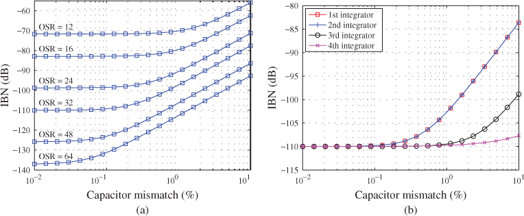
Figure 2.5 illustrates this increasing impact of capacitor mismatch with OSR and with the stage of the cascade being considered. Note that results displayed correspond to worst-case estimations of the IBN based on Equation 2.15 with ![]() . More accurate estimations would require Monte Carlo simulation of the modulator behavioral model considering the particular implementation of each integrator gain coefficient in terms of unit capacitors.
. More accurate estimations would require Monte Carlo simulation of the modulator behavioral model considering the particular implementation of each integrator gain coefficient in terms of unit capacitors.
Figure 2.5 Influence of capacitor mismatch on the in-band noise of a 2-1-1 SC-![]() M: (a) considering the same mismatch error in all integrators and (b) individual impact of the mismatch error in each integrator for OSR = 32. Worst-case estimations of IBN considering
M: (a) considering the same mismatch error in all integrators and (b) individual impact of the mismatch error in each integrator for OSR = 32. Worst-case estimations of IBN considering ![]() in Equation 2.15.
in Equation 2.15.
2.4 Integrator Settling Error in SC- Ms
Ms
Speed limitations in SC integrators due to the limited dynamic response of amplifiers cause errors in the charge transfer. The impact of the resulting error in the integrator output voltage settling error on the modulator performance will be higher, the higher the sampling frequency. As the clock frequency increases in SC-![]() Ms to cope with larger conversion bandwidths, integrator settling error becomes one of the bottlenecks for their practical implementation. On the one hand, the time slot for the integrator operation gets reduced; on the other hand, the amplifier dynamic requirements must be minimized to optimize the modulator power consumption. Therefore, an adequate understanding of the mechanisms degrading the settling of SC integrators and an accurate quantification of the generated errors become mandatory to obtain efficient
Ms to cope with larger conversion bandwidths, integrator settling error becomes one of the bottlenecks for their practical implementation. On the one hand, the time slot for the integrator operation gets reduced; on the other hand, the amplifier dynamic requirements must be minimized to optimize the modulator power consumption. Therefore, an adequate understanding of the mechanisms degrading the settling of SC integrators and an accurate quantification of the generated errors become mandatory to obtain efficient ![]() designs.
designs.
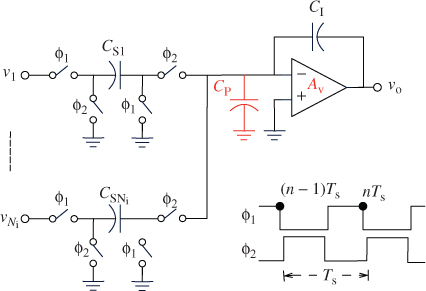
2.4.1 Behavioral Model for the Integrator Settling
The behavioral model of the transient response for SC FE integrators included in this section is based on the analysis presented in [6]. The model includes the effect of the amplifier dynamic limitations, such as finite gain-bandwidth product (GB) and slew rate (SR), on the charge transfer during both the integration and sampling phases. Also, parasitic capacitors associated with amplifiers and switches, as well as the capacitor load at the integrator output—which changes from integration to sampling—are taken into account. To accurately describe the dynamic performance and determine the integrator output voltage, the equivalent circuit shown in Figure 2.6 is solved in the behavioral model. In the circuit scheme, the SC integrator under study is considered to have ![]() input branches and another SC integrator acting as a load—that is, the No
input branches and another SC integrator acting as a load—that is, the No
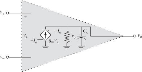
input branches of the latter are connected to the output of the former. On the other hand, the amplifier is modeled as shown in Figure 2.7, with a single-pole dynamic (to account for the finite bandwidth) and a nonlinear characteristic with maximum output current ![]() (to account for the limited SR).1
(to account for the limited SR).1
Figure 2.6 SC FE integrator under consideration followed by a loading SC integrator.
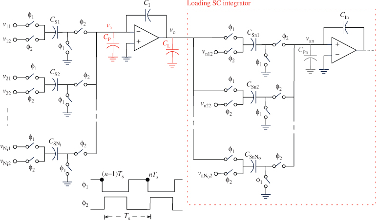
Figure 2.7 Amplifier single-pole model with limited output current.
The analysis of this model for the incomplete settling error begins with the computation of the equivalent capacitive load at the amplifier output node during both the sampling (![]() ) and integration (
) and integration (![]() ) phases, respectively given by,
) phases, respectively given by,

where ![]() represents the sampling capacitor of the
represents the sampling capacitor of the ![]() th SC input branch of the integrator under consideration,
th SC input branch of the integrator under consideration, ![]() is the sampling capacitor of the
is the sampling capacitor of the ![]() th SC input branch of the load integrator,
th SC input branch of the load integrator, ![]() is the parasitic capacitor at the summation node of the input SC branches, and
is the parasitic capacitor at the summation node of the input SC branches, and ![]() is the amplifier load capacitor.
is the amplifier load capacitor.
The settling model is analyzed during a complete clock cycle (during both clock phases) considering the different possibilities for the amplifier dynamic operation—that is, linearly or in slew—and keeping track of the voltage at both the integrator output ![]() and the amplifier summation node
and the amplifier summation node ![]() . Therefore, the error in the integrator output voltage at the end of one sampling-integration process can be accurately obtained.
. Therefore, the error in the integrator output voltage at the end of one sampling-integration process can be accurately obtained.
Let ![]() and
and ![]() be the respective amplifier input and output voltages at the end of a preceding integration phase, which will serve as initial conditions to derive of the integrator evolution during a complete clock cycle. The voltage at the amplifier summation node at the end of the next sampling phase—that is, at
be the respective amplifier input and output voltages at the end of a preceding integration phase, which will serve as initial conditions to derive of the integrator evolution during a complete clock cycle. The voltage at the amplifier summation node at the end of the next sampling phase—that is, at ![]() —, can be accurately obtained as [6],
—, can be accurately obtained as [6],

where ![]() is the duration of the SR-limited integrator settling (relative to
is the duration of the SR-limited integrator settling (relative to ![]() ) given by,
) given by,
sgn() is the sign function, and ![]() represents the value of
represents the value of ![]() at the beginning of the sampling phase, which can be computed as,
at the beginning of the sampling phase, which can be computed as,
2.19 ![]()
where ![]() is the voltage across capacitor
is the voltage across capacitor ![]() .2
.2
The integrator output voltage at the end of the sampling phase can be obtained as,
as opposed to the ideal situation in which ![]() .
.
Note from Equations 2.17 and 2.20 that, for the integrator model in Figure 2.6, the amplifier gain-bandwidth product and output SR during sampling are obtained as:
During the integration phase, the incomplete settling model is evaluated proceeding in a similar way as done for the sampling phase. Thus, at the end of the subsequent integration phase—that is, at ![]() —, the value of
—, the value of ![]() is given by [3],
is given by [3],

where ![]() is the duration of the SR-limited integrator settling (relative to
is the duration of the SR-limited integrator settling (relative to ![]() ), given by
), given by
2.23 ![]()
and ![]() represents the value of
represents the value of ![]() at the beginning of the integration phase. The latter can be computed as
at the beginning of the integration phase. The latter can be computed as
2.24 
where ![]() are the voltages connected to the input of the
are the voltages connected to the input of the ![]() th SC branch during
th SC branch during ![]() , respectively, and
, respectively, and ![]() represents:
represents:
2.25 ![]()
The integrator output voltage at the end of the integration phase can be obtained as,

as opposed to the ideal integration process with no dynamic limitations, in which the last two terms in Equation 2.26 are null.
The amplifier gain-bandwidth product and output SR during this phase can be obtained similarly as for the sampling phase to be:

Figure 2.8 illustrates how the equations above can be concatenated to accurately keep track of the summation and output voltages of an SC integrator over the clock periods. They can be easily incorporated into CAD tools for the behavioral simulation of SC-![]() Ms—or SC circuits in general. Moreover, the previous model can be easily extrapolated to other operating conditions: integration and sampling phases with different durations, different switching loading conditions at the integrator output, to include the parasitic capacitance of the switches, etc.
Ms—or SC circuits in general. Moreover, the previous model can be easily extrapolated to other operating conditions: integration and sampling phases with different durations, different switching loading conditions at the integrator output, to include the parasitic capacitance of the switches, etc.
Figure 2.8 Illustration of the influence of switching load conditions on the transient response of an SC integrator: (a) loading SC branches are not considered and (b) one loading SC branch with a 0.5-pF capacitor is considered. (Vertical dashed lines indicate time positions ![]() where the integrator ends an SR-limited response and starts evolving linearly). Parameters used are (Figures 2.6 and 2.7):
where the integrator ends an SR-limited response and starts evolving linearly). Parameters used are (Figures 2.6 and 2.7): ![]() ,
, ![]() ,
, ![]() ,
, ![]() ,
, ![]() ,
, ![]() ,
, ![]() , and
, and ![]() for the SC integrator under consideration,
for the SC integrator under consideration, ![]() and
and ![]() for the loading SC integrator, and
for the loading SC integrator, and ![]() .
.

2.4.2 Linear Effect of Finite Amplifier Gain-Bandwidth Product
The model for the transient response of SC integrators described earlier can be easily incorporated into behavioral simulators for SC-![]() Ms to accurately quantify the influence of settling errors on the modulator performance—in terms of both the increased in-band noise and the generated distortion. Besides this behavioral model, it is often useful to work at the early design stages (high-level design) with closed-form expressions which, although being coarse approximations of the behavioral model, can help to gain insight of the influence of settling parameters on different modulator topologies. For this purpose, a linear transient response will be assumed for SC integrators in this section, as if settling error was determined only by the finite amplifier GB with no limitation on the SR.
Ms to accurately quantify the influence of settling errors on the modulator performance—in terms of both the increased in-band noise and the generated distortion. Besides this behavioral model, it is often useful to work at the early design stages (high-level design) with closed-form expressions which, although being coarse approximations of the behavioral model, can help to gain insight of the influence of settling parameters on different modulator topologies. For this purpose, a linear transient response will be assumed for SC integrators in this section, as if settling error was determined only by the finite amplifier GB with no limitation on the SR.
With these considerations in mind, the finite difference equation of an SC FE integrator can be obtained from Equations 2.17, 2.20, 2.22, and 2.26 to be,
where only one input branch is considered for simplicity. The settling error associated with the linearly limited transient response is represented by ![]() , which thus contains terms in
, which thus contains terms in ![]() and in
and in ![]() —with GB in rad s
—with GB in rad s![]() . If settling errors associated with integration dominate on the overall defective settling over those originated during sampling, the linear settling error can be simply reduced to:
. If settling errors associated with integration dominate on the overall defective settling over those originated during sampling, the linear settling error can be simply reduced to:
2.29 ![]()
Transforming Equation 2.28 to the ![]() -domain, the integrator output results in,
-domain, the integrator output results in,
2.30 ![]()
so that, under the assumptions earlier, settling error translates into a gain error in the ideal ITF, whose effect on the IBN of SC-![]() Ms can be computed in a similar way as formerly done for capacitor mismatch in Section 2.3. Therefore, Equations 2.13–2.14 still hold for quantifying the effect of linear defective settling to first order, just by replacing
Ms can be computed in a similar way as formerly done for capacitor mismatch in Section 2.3. Therefore, Equations 2.13–2.14 still hold for quantifying the effect of linear defective settling to first order, just by replacing ![]() with
with ![]() .
.
Figure 2.9 illustrates the effect of the finite amplifier GB on single-loop and cascade SC-![]() Ms. The in-band noise of second- and third-order single loops and of a 2-1-1 cascade is computed considering both the behavioral model for the integrator settling in Section 2.4.1 and the approximated closed-form expressions of the generated gain error. Large amplifier output currents have been used in behavioral simulations to make the influence of SR limitation negligible and thus consider linear errors only. Note that, as expected, cascades
Ms. The in-band noise of second- and third-order single loops and of a 2-1-1 cascade is computed considering both the behavioral model for the integrator settling in Section 2.4.1 and the approximated closed-form expressions of the generated gain error. Large amplifier output currents have been used in behavioral simulations to make the influence of SR limitation negligible and thus consider linear errors only. Note that, as expected, cascades ![]() Ms are more sensitive to GB limitations that single loops. Usually, an amplifier GB of 1–2
Ms are more sensitive to GB limitations that single loops. Usually, an amplifier GB of 1–2![]() is sufficient for single-loop modulators to achieve full performance, whereas the requirement increases to 3–10
is sufficient for single-loop modulators to achieve full performance, whereas the requirement increases to 3–10![]() for cascade
for cascade ![]() Ms as the oversampling ratio increases.
Ms as the oversampling ratio increases.
Figure 2.9 Simulation results for the influence of amplifier GB on the in-band noise of SC-![]() Ms: (a) second- and third-order loops and (b) 2-1-1 cascade. Approximated results have been obtained from Equations 2.13 and 2.15 with
Ms: (a) second- and third-order loops and (b) 2-1-1 cascade. Approximated results have been obtained from Equations 2.13 and 2.15 with ![]() .
.

2.4.3 Nonlinear Effect of Finite Amplifier Slew Rate
Contrary to errors arising from finite amplifier GB, finite amplifier SR caused by limited output current capability has a purely nonlinear effect on the performance of ![]() Ms, generating distortion and an increase in the noise floor.
Ms, generating distortion and an increase in the noise floor.
For the case of single-loop SC-![]() Ms, SR-limited integrator dynamics basically translate into distortion. Figure 2.10 illustrates the impact of amplifier SR on a single-bit third-order
Ms, SR-limited integrator dynamics basically translate into distortion. Figure 2.10 illustrates the impact of amplifier SR on a single-bit third-order ![]() M operating with an oversampling ratio of 64. An input tone with
M operating with an oversampling ratio of 64. An input tone with ![]() (
(![]() amplitude) and frequency equal to
amplitude) and frequency equal to ![]() is applied to the modulator in behavioral simulations. Note from the presented results that, depending on the amplifier GB, an SR of 4–8
is applied to the modulator in behavioral simulations. Note from the presented results that, depending on the amplifier GB, an SR of 4–8![]() is enough to reduce the power of generated distortion to a level that does not affect IBN.
is enough to reduce the power of generated distortion to a level that does not affect IBN.
Figure 2.10 Simulation results for a third-order SC-![]() M with
M with ![]() under the influence of finite amplifier slew rate: (a) effect on the in-band noise and (b) effect on the output spectrum for
under the influence of finite amplifier slew rate: (a) effect on the in-band noise and (b) effect on the output spectrum for ![]() . Input signal with
. Input signal with ![]() and
and ![]() . Generated distortion is included in the IBN computation.
. Generated distortion is included in the IBN computation.

For the case of cascade SC-![]() Ms, finite amplifier SR generates distortion as well as an increase in the noise floor due to noise leakages, as shown in Figure 2.11. For that reason, SR requirements are larger than for single loops and usually range from 4 to
Ms, finite amplifier SR generates distortion as well as an increase in the noise floor due to noise leakages, as shown in Figure 2.11. For that reason, SR requirements are larger than for single loops and usually range from 4 to ![]() depending on the amplifier GB—the larger the GB, the lower the required SR.
depending on the amplifier GB—the larger the GB, the lower the required SR.
Figure 2.11 Simulation results for a 2-1-1 SC-![]() M with
M with ![]() under the influence of finite amplifier slew rate: (a) effect on the in-band noise and (b) effect on the output spectrum for
under the influence of finite amplifier slew rate: (a) effect on the in-band noise and (b) effect on the output spectrum for ![]() . Input signal with
. Input signal with ![]() and
and ![]() . Generated distortion is included in the IBN computation.
. Generated distortion is included in the IBN computation.

Finally, note that the SR-limited integrator dynamic is a nonlinear signal-dependent phenomenon whose occurrence frequency during the modulator operation is directly determined by the signal level at the integrators inputs. Therefore, the ultimate way to reduce SR requirements on an SC-![]() M is to resort to multibit internal quantization.
M is to resort to multibit internal quantization.
2.4.4 Effect of Finite Switch On-Resistance
Switches in the SC branches of ![]() Ms are implemented with MOSFETs—using either single nMOS or pMOS transistors, or CMOS transmission gates—that operate in the triode region when on and thus exhibit in practice a nonzero on-resistance.
Ms are implemented with MOSFETs—using either single nMOS or pMOS transistors, or CMOS transmission gates—that operate in the triode region when on and thus exhibit in practice a nonzero on-resistance.
If the on-resistance of the switches is the only nonideality accounted for in the operation of an SC integrator, it clearly leads to an incomplete charge transfer due to the ![]() time constant that is created in the SC branch. Considering for instance the scheme in Figure 2.12, the integrator output voltage can be obtained as [3],
time constant that is created in the SC branch. Considering for instance the scheme in Figure 2.12, the integrator output voltage can be obtained as [3],
Figure 2.12 SC FE integrator with a single input branch.

2.31 
where ![]() represents the charging error in
represents the charging error in ![]() during
during ![]() related to the on-resistance of switches
related to the on-resistance of switches ![]() and
and ![]() and
and ![]() represents the error in the charge transfer from
represents the error in the charge transfer from ![]() to
to ![]() during
during ![]() related to the on-resistance of switches
related to the on-resistance of switches ![]() and
and ![]() . If
. If ![]() is the on-resistance of a single switch, assuming that all switches are of the same size and that both clock phases have the same duration leads to:
is the on-resistance of a single switch, assuming that all switches are of the same size and that both clock phases have the same duration leads to:
2.32 ![]()
Therefore, charge transfer error due to the on-resistance of the switches translates into a gain error in the ideal ITF, whose effect on the IBN of SC-![]() Ms can be computed in a similar way as formerly done in Sections 2.3 or 2.4.2. Therefore, finite switch on-resistance will have considerably lower impact on
Ms can be computed in a similar way as formerly done in Sections 2.3 or 2.4.2. Therefore, finite switch on-resistance will have considerably lower impact on ![]() single loops than on cascades.
single loops than on cascades.
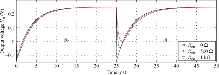
Besides the former discussion on how the switch on-resistance, as a stand-alone nonideality, affects an SC integrator, its effect is better accounted for in practice in combination with the limited amplifier dynamics. Figure 2.13 shows electrical simulation results to illustrate the influence of ![]() on the transient response of the same SC integrator formerly considered in Figure 2.8. Only one clock cycle is shown here to gain in visibility of the
on the transient response of the same SC integrator formerly considered in Figure 2.8. Only one clock cycle is shown here to gain in visibility of the ![]() effect. Note that the linear amplifier response is slowed down as the on-resistance increases, affecting the integrator settling during both the sampling and the integration phase. To incorporate this effect into behavioral simulations, the effective amplifier GB during both clock phases can be approximated to [3],
effect. Note that the linear amplifier response is slowed down as the on-resistance increases, affecting the integrator settling during both the sampling and the integration phase. To incorporate this effect into behavioral simulations, the effective amplifier GB during both clock phases can be approximated to [3],
2.33 
where ![]() and
and ![]() represent the
represent the ![]() poles introduced by loading SC branch and by the input SC branch, respectively, and
poles introduced by loading SC branch and by the input SC branch, respectively, and ![]() and
and ![]() are respectively given by Equations 2.21 and 2.27.
are respectively given by Equations 2.21 and 2.27.
Figure 2.13 Illustration of the influence of the switch on-resistance on the transient response of an SC integrator with a loading SC branch. Simulation parameters used are same as those for Figure 2.8 for comparison purposes.
In addition, results presented in Section 2.4.2 for the linear effect of finite amplifier GB on the IBN of SC-![]() Ms can be easily refined to include the slow-down effect of the switches
Ms can be easily refined to include the slow-down effect of the switches ![]() . To that purpose, the following gain error
. To that purpose, the following gain error
2.34 ![]()
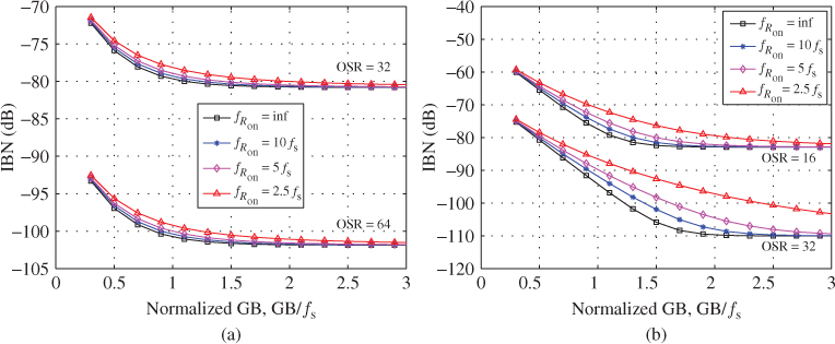
can be considered in Equations 2.13 and 2.14. Figure 2.14 illustrates the combined linear effect of the finite amplifier GB and finite switch on-resistance on a third-order single loop and on a 2-1-1 cascade SC-![]() M. The lower sensitivity of single loops to these errors is clear and a switch on-resistance such that
M. The lower sensitivity of single loops to these errors is clear and a switch on-resistance such that ![]() is 4–5
is 4–5![]() is sufficient, in combination with the limited amplifier GB, to achieve full performance. This requirement for the
is sufficient, in combination with the limited amplifier GB, to achieve full performance. This requirement for the ![]() usually increases to 10–20
usually increases to 10–20![]() for cascade
for cascade ![]() Ms as the oversampling increases.
Ms as the oversampling increases.
Figure 2.14 Influence of switch on-resistance on the in-band noise of SC-![]() Ms: (a) third-order loop and (b) 2-1-1 cascade. Approximated results have been obtained from Equations 2.13 and 2.15 with
Ms: (a) third-order loop and (b) 2-1-1 cascade. Approximated results have been obtained from Equations 2.13 and 2.15 with ![]() .
.
2.5 Circuit Noise in SC- Ms
Ms
Electronic noise generated in transistors and resistors is present in any circuit implementation and imposes an ultimate limit to the resolution of ADCs. However, its impact is more severe in DT-![]() Ms that employ SC-techniques due to the white spectrum of the main circuit noise sources. In an SC-
Ms that employ SC-techniques due to the white spectrum of the main circuit noise sources. In an SC-![]() M, these broadband noise components are sampled together with the input signal at the clock frequency, so that they fold over the modulator passband and may cause a considerable increase of the modulator in-band noise due to aliasing.
M, these broadband noise components are sampled together with the input signal at the clock frequency, so that they fold over the modulator passband and may cause a considerable increase of the modulator in-band noise due to aliasing.
As stated in Section 2.1, the influence of nonidealities on the IBN of ![]() Ms is mainly determined by the location of the corresponding noise source in the modulator. With respect to circuit noise, all SC integrators in a
Ms is mainly determined by the location of the corresponding noise source in the modulator. With respect to circuit noise, all SC integrators in a ![]() M add noise in the modulator passband, but the role of the front-end integrator is indeed dominant. When referred to the modulator input, noise power contributed by the remaining integrators is divided by the gain of preceding integrators within the modulator passband, so their influence strongly diminishes while moving from front-end to back-end integrators. Conversely, no shaping takes place at the modulator input and the first integrator has thus to fulfill the noise and linearity requirements of the complete
M add noise in the modulator passband, but the role of the front-end integrator is indeed dominant. When referred to the modulator input, noise power contributed by the remaining integrators is divided by the gain of preceding integrators within the modulator passband, so their influence strongly diminishes while moving from front-end to back-end integrators. Conversely, no shaping takes place at the modulator input and the first integrator has thus to fulfill the noise and linearity requirements of the complete ![]() M.
M.
Let us consider the SC integrator in Figure 2.15a to be the front-end integrator of an SC-![]() M. Two input SC branches are considered: the one including capacitor
M. Two input SC branches are considered: the one including capacitor ![]() is assumed to sample the modulator input signal (
is assumed to sample the modulator input signal (![]() ), whereas the one including capacitor
), whereas the one including capacitor ![]() samples the DAC feedback signal (
samples the DAC feedback signal (![]() ). The main sources of circuit noise in SC integrators have been incorporated into the equivalent models in Figures 2.15b and 2.15c during each of the clock phases, namely, thermal noise generated in the switches and noise generated in the amplifier—both thermal and flicker components to be considered.3
). The main sources of circuit noise in SC integrators have been incorporated into the equivalent models in Figures 2.15b and 2.15c during each of the clock phases, namely, thermal noise generated in the switches and noise generated in the amplifier—both thermal and flicker components to be considered.3
Figure 2.15 Circuit noise analysis in an SC integrator: (a) SC FE integrator with two input paths (single-ended version), (b) equivalent circuit model for sampling, with noise sources due to switches active during ![]() and (c) equivalent circuit model for integration, with noise sources due to switches active during
and (c) equivalent circuit model for integration, with noise sources due to switches active during ![]() and due to the amplifier.
and due to the amplifier.

Figure 2.15b shows the model for the thermal noise introduced by switches controlled by clock phase ![]() . For both SC branches, the two active switches are assumed to have the same on-resistance (
. For both SC branches, the two active switches are assumed to have the same on-resistance (![]() ) and they are in series with a noise voltage source
) and they are in series with a noise voltage source ![]() . The PSD of each of these noise sources in a single-sided frequency representation is thus
. The PSD of each of these noise sources in a single-sided frequency representation is thus ![]() , where
, where ![]() is Boltzmann's constant and
is Boltzmann's constant and ![]() is the absolute temperature. Each of the noise sources generates a sample-and-held noise component in the corresponding capacitor voltage given by the well-known
is the absolute temperature. Each of the noise sources generates a sample-and-held noise component in the corresponding capacitor voltage given by the well-known ![]() expression due to the foldover effect [7–9]:
expression due to the foldover effect [7–9]:
Figure 2.15c shows the model for the thermal noise introduced by switches controlled by clock phase ![]() and for the noise in the amplifier. These switches originate an additional noise component in the capacitor voltage of the corresponding SC branch, similarly given by Equation 2.35. On the other hand, a single-pole model is assumed for the amplifier and its equivalent input noise is modeled by a voltage source
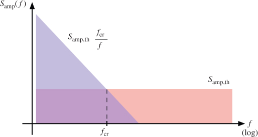
and for the noise in the amplifier. These switches originate an additional noise component in the capacitor voltage of the corresponding SC branch, similarly given by Equation 2.35. On the other hand, a single-pole model is assumed for the amplifier and its equivalent input noise is modeled by a voltage source ![]() at the positive input terminal. As illustrated in Figure 2.16, the amplifier noise is basically determined by a broadband thermal component and a narrowband flicker component, so that
at the positive input terminal. As illustrated in Figure 2.16, the amplifier noise is basically determined by a broadband thermal component and a narrowband flicker component, so that
Figure 2.16 Illustration of the PSD of the amplifier noise showing the contributions of ![]() and thermal noise.
and thermal noise.
where ![]() represents the amplifier thermal noise PSD referred to its input and
represents the amplifier thermal noise PSD referred to its input and ![]() represents the amplifier corner frequency—that is, the frequency at which
represents the amplifier corner frequency—that is, the frequency at which ![]() noise is equal to the thermal noise.4 The amplifier noise generates correlated sample-and-held noise components in the integrator sampling capacitors that can be obtained as
noise is equal to the thermal noise.4 The amplifier noise generates correlated sample-and-held noise components in the integrator sampling capacitors that can be obtained as
where the amplifier noise bandwidth ![]() is required to account for the foldover effect of thermal noise. As shown in [3], it can be estimated as
is required to account for the foldover effect of thermal noise. As shown in [3], it can be estimated as ![]() , with
, with ![]() given by Equation 2.27.
given by Equation 2.27.
Adding up the former circuit noise components in the SC integrator, the total input-referred5 noise PSD yields [3]
where the factor 2 multiplying ![]() accounts for the contributions of switches controlled by
accounts for the contributions of switches controlled by ![]() and
and ![]() , whereas the factor 2 before the brackets accounts for the actual fully-differential implementation of the SC integrator, in which the number of SC branches and thus of switches doubles in comparison to the single-ended scheme in Figure 2.15. Replacing Equations 2.35 and 2.37 in 2.38, the total input-referred noise PSD of the front-end integrator of an SC-
, whereas the factor 2 before the brackets accounts for the actual fully-differential implementation of the SC integrator, in which the number of SC branches and thus of switches doubles in comparison to the single-ended scheme in Figure 2.15. Replacing Equations 2.35 and 2.37 in 2.38, the total input-referred noise PSD of the front-end integrator of an SC-![]() M can thus be approximated to be
M can thus be approximated to be
2.39 ![]()
in which the approximation ![]() for
for ![]() has been used for simplicity.
has been used for simplicity.
The input-referred IBN of an SC-![]() M due to circuit noise can be easily obtained by integrating the former expression over the input signal bandwidth, so that
M due to circuit noise can be easily obtained by integrating the former expression over the input signal bandwidth, so that

in which the ![]() noise component has been integrated from a frequency
noise component has been integrated from a frequency ![]() to exclude DC due to its logarithmic nature.
to exclude DC due to its logarithmic nature.
For an SC-![]() M to achieve a given noise performance, the sum of all three components in Equation 2.40 have to meet the demanded noise floor. Note that:
M to achieve a given noise performance, the sum of all three components in Equation 2.40 have to meet the demanded noise floor. Note that:
- For a given OSR, to reduce the contribution of the switches' thermal noise, the size of the sampling capacitors at the modulator input must be increased, which results in larger speed requirements for the amplifier and thus in larger power consumption.
- For a given OSR, to reduce the contribution of the amplifier thermal noise, its GB must be reduced as much as the integrator settling requirements allow.
- To reduce the flicker contribution the amplifier corner frequency must be kept low. In low-bandwidth applications, cancelation techniques such as correlated double sampling (CDS) or chopper are often required for further reduction of the
 component [10].
2.6 Clock Jitter in SC- Ms
Ms
Discrete-time ![]() Ms are affected in practice by timing uncertainties6 in the clock phases that control the SC operation. However, they exhibit largertolerance to clock jitter than Nyquist converters, because jitter sensitivity is reduced by the modulator OSR [12].
Ms are affected in practice by timing uncertainties6 in the clock phases that control the SC operation. However, they exhibit largertolerance to clock jitter than Nyquist converters, because jitter sensitivity is reduced by the modulator OSR [12].
The effect of clock jitter in SC-![]() Ms is mainly limited to a sampling uncertainty of the modulator input signal. Timing uncertainties during the integration phase only cause an extra error to be added to the integrator settling error and their influence can be neglected in practice, whereas the contributions of other integrators than the front-end one will be reduced by the noise shaping. Therefore, different SC-
Ms is mainly limited to a sampling uncertainty of the modulator input signal. Timing uncertainties during the integration phase only cause an extra error to be added to the integrator settling error and their influence can be neglected in practice, whereas the contributions of other integrators than the front-end one will be reduced by the noise shaping. Therefore, different SC-![]() Ms exhibit similar sensitivity to clock jitter [13].
Ms exhibit similar sensitivity to clock jitter [13].
Sampling time uncertainty causes a nonuniform sampling of the modulator input signal that results in an increase of the in-band error power. The magnitude of this increase is usually estimated for SC-![]() Ms assuming random statistical properties for the clock jitter [12]. For a modulator input sinewave
Ms assuming random statistical properties for the clock jitter [12]. For a modulator input sinewave ![]() as shown in Figure 2.17, an uncertainty of
as shown in Figure 2.17, an uncertainty of ![]() in the sampling instant causes an error in the sampled signal given by:
in the sampling instant causes an error in the sampled signal given by:
Figure 2.17 Illustration of nonuniform sampling of a signal due to clock jitter. The gray shaded areas represent the timing uncertainties.

2.41 ![]()
Under the assumption of white jitter, the power of this modulated error distributes uniformly, so that only a fraction of it is located within the ![]() M passband. The in-band noise due to clock jitter can thus be easily obtained as
M passband. The in-band noise due to clock jitter can thus be easily obtained as

where ![]() represents the standard deviation of the timing uncertainty. Taking into account that
represents the standard deviation of the timing uncertainty. Taking into account that ![]() and
and ![]() , an upper bound can be calculated for Equation 2.42
, an upper bound can be calculated for Equation 2.42
showing that the sensitivity of SC-![]() Ms to clock jitter is reduced by
Ms to clock jitter is reduced by ![]() .
.
2.7 Sources of Distortion in SC- Ms
Ms
Analog devices used for the implementation of ![]() Ms exhibit in practice a certain nonlinearity. These nonlinearities generate distortion and thus limit the peak SNDR attainable for high input amplitudes. Nevertheless, deriving closed-form expressions for the distortion generated in a
Ms exhibit in practice a certain nonlinearity. These nonlinearities generate distortion and thus limit the peak SNDR attainable for high input amplitudes. Nevertheless, deriving closed-form expressions for the distortion generated in a ![]() M is in general much more awkward than analyzing the effect of linear errors. Therefore, several simplifications are often made to handle nonlinearities. First, only the sources of distortion associated with the front-end integrator in the
M is in general much more awkward than analyzing the effect of linear errors. Therefore, several simplifications are often made to handle nonlinearities. First, only the sources of distortion associated with the front-end integrator in the ![]() M are considered, as they directly add to the modulator signal with no attenuation and thus dominate the overall modulator nonlinearity. Distortion generated in subsequent integrators is suppressed by the increasing noise shaping when referred to the modulator input, so that their contributions can be considered negligible in practice. Second, each source of nonlinearity is conceived as a small deviation from the ideal linear behavior—that is, as a weak nonlinearity—that affects the modulator performance in an additive way.
M are considered, as they directly add to the modulator signal with no attenuation and thus dominate the overall modulator nonlinearity. Distortion generated in subsequent integrators is suppressed by the increasing noise shaping when referred to the modulator input, so that their contributions can be considered negligible in practice. Second, each source of nonlinearity is conceived as a small deviation from the ideal linear behavior—that is, as a weak nonlinearity—that affects the modulator performance in an additive way.
Figure 2.18 illustrates the main sources of distortion in an SC integrator, in which a fully-differential topology is assumed for the suppression of even-order harmonics. In SC-![]() Ms, linearity is basically limited by the voltage dependency of capacitors, of the switches on-resistance, and of the amplifier gain, as well as by the SR-limited integrator dynamics (already discussed in Section 2.4.3). Distortion arising from charge injection in the switches can be neglected if clock phases with delayed falling edges are employed [14]. Besides, given the highly linear capacitors that present mixed-mode technological processes offer—such as MiM and MoM capacitors—their effect will not be further considered here.7 The influence of the nonlinearity of the switches and of the amplifier gain will be discussed later.
Ms, linearity is basically limited by the voltage dependency of capacitors, of the switches on-resistance, and of the amplifier gain, as well as by the SR-limited integrator dynamics (already discussed in Section 2.4.3). Distortion arising from charge injection in the switches can be neglected if clock phases with delayed falling edges are employed [14]. Besides, given the highly linear capacitors that present mixed-mode technological processes offer—such as MiM and MoM capacitors—their effect will not be further considered here.7 The influence of the nonlinearity of the switches and of the amplifier gain will be discussed later.
Figure 2.18 Main sources of distortion in a fully-differential SC integrator.

2.7.1 Nonlinear Amplifier Gain
The DC gain of an amplifier exhibits in practice a voltage-dependent characteristic, because the output resistance of the amplifier output transistors decreases as the amplifier output voltage deviates from the quiescent point. Figure 2.19 illustrates this effect with electrical simulations results of a folded-cascode amplifier designed in a 2.5-V 0.25-![]() m CMOS process. Note that the amplifier DC gain is about 8500 (78.5 dB) at the common-mode output voltage, but it decreases for increasing output levels and drops abruptly near the amplifier saturation region.
m CMOS process. Note that the amplifier DC gain is about 8500 (78.5 dB) at the common-mode output voltage, but it decreases for increasing output levels and drops abruptly near the amplifier saturation region.
Figure 2.19 Illustration of the dependency of the amplifier gain on the output voltage level.

The influence of the amplifier gain nonlinearity can be easily incorporated into the leaky integrator model in Section 2.2, so that the difference equation in Equation 2.2 can be rewritten as [3]
2.44 
where ![]() represents the effective amplifier gain at the output voltage corresponding to clock cycle
represents the effective amplifier gain at the output voltage corresponding to clock cycle ![]() and
and ![]() corresponds to that of clock cycle
corresponds to that of clock cycle ![]() . As will be shown in Section 3.3, solving this difference equation in an iterative way, together with a table look-up for the amplifier gain, allows for accurately accounting for the voltage dependency of the amplifier gain in transient behavioral simulations—in spite of the nonlinearity being weak or strong!
. As will be shown in Section 3.3, solving this difference equation in an iterative way, together with a table look-up for the amplifier gain, allows for accurately accounting for the voltage dependency of the amplifier gain in transient behavioral simulations—in spite of the nonlinearity being weak or strong!
For weak nonlinearities, a polynomial approximation can be used for modeling the voltage dependency near the quiescent point and for obtaining rough estimations of the generated distortion. Let us assume that the amplifier gain of the front-end integrator in an SC-![]() M, such as that shown in Figure 2.18, is expressed as
M, such as that shown in Figure 2.18, is expressed as
2.45 ![]()
where ![]() represents the
represents the ![]() th-order voltage-gain coefficient of the amplifier DC gain. If a sinewave with amplitude
th-order voltage-gain coefficient of the amplifier DC gain. If a sinewave with amplitude ![]() is applied at the modulator input, the input-referred distortion of the third-order harmonic can be estimated as [3, 15]
is applied at the modulator input, the input-referred distortion of the third-order harmonic can be estimated as [3, 15]
2.46 
where ![]() is the parasitic capacitor at the amplifier input nodes. Note that decreasing the integrator gain coefficient clearly helps to reduce distortion. However, the most direct way to reduce the effect of the amplifier gain nonlinearity is increasing the value of the amplifier gain itself [3, 13].
is the parasitic capacitor at the amplifier input nodes. Note that decreasing the integrator gain coefficient clearly helps to reduce distortion. However, the most direct way to reduce the effect of the amplifier gain nonlinearity is increasing the value of the amplifier gain itself [3, 13].
2.7.2 Nonlinear Switch On-Resistance
Switches in SC-![]() Ms are usually implemented as CMOS transmission gates, so that, at least, either the nMOS or the pMOS transistors are on for a given voltage level to be transmitted. Figure 2.20a sketches the on-conductance of nMOS and pMOS switches, assuming that they exhibit a resistance in the triode region that can be approximated to [3, 16]
Ms are usually implemented as CMOS transmission gates, so that, at least, either the nMOS or the pMOS transistors are on for a given voltage level to be transmitted. Figure 2.20a sketches the on-conductance of nMOS and pMOS switches, assuming that they exhibit a resistance in the triode region that can be approximated to [3, 16]

where ![]() represents the switch input voltage—that is, the common-mode voltage of the drain and source terminals. The on-resistance of the CMOS transmission gate is thus obtained as
represents the switch input voltage—that is, the common-mode voltage of the drain and source terminals. The on-resistance of the CMOS transmission gate is thus obtained as ![]() , warranting a rail-to-rail operation of the switch as long as
, warranting a rail-to-rail operation of the switch as long as ![]() .8 Figure 2.20b shows electrical simulation results of a transmission gate in a 2.5-V 0.25-
.8 Figure 2.20b shows electrical simulation results of a transmission gate in a 2.5-V 0.25-![]() m CMOS process, in which the voltage dependency of the switch on-resistance is clearly visible.
m CMOS process, in which the voltage dependency of the switch on-resistance is clearly visible.
Figure 2.20 Illustration of a switch on-state performance: (a) sketch of the on-conductance versus input voltage and (b) simulation results of the on-resistance versus input voltage in a 2.5-V 0.25-![]() m CMOS process.
m CMOS process.

To analyze the relative influence of the different switches in the front-end integrator of an SC-![]() M on the generated distortion, let us consider the schematic in Figure 2.18. The modulator input signal is sampled on capacitors
M on the generated distortion, let us consider the schematic in Figure 2.18. The modulator input signal is sampled on capacitors ![]() through switches
through switches ![]() and
and ![]() during
during ![]() . As switches
. As switches ![]() are connected to the modulator input, their on-resistances directly depend on the modulator input level and are the dominant source of distortion. However, switches
are connected to the modulator input, their on-resistances directly depend on the modulator input level and are the dominant source of distortion. However, switches ![]() have one of their terminals connected to the common-mode voltage—that is, to a voltage that remains approximately constant over time—so that the voltage level of these switches is not expected to change much over the clock periods [5]. As a result, the distortion introduced by switches
have one of their terminals connected to the common-mode voltage—that is, to a voltage that remains approximately constant over time—so that the voltage level of these switches is not expected to change much over the clock periods [5]. As a result, the distortion introduced by switches ![]() will be considerably lower than that of switches
will be considerably lower than that of switches ![]() . The same reasoning can be applied to switches
. The same reasoning can be applied to switches ![]() and
and ![]() during
during ![]() : switches
: switches ![]() have one terminal connected to a fixed voltage—the common-mode voltage, as depicted in Figure 2.18, or the DAC feedback voltage—and switches
have one terminal connected to a fixed voltage—the common-mode voltage, as depicted in Figure 2.18, or the DAC feedback voltage—and switches ![]() are connected to the virtual ground of the amplifier. Their influence on the generated distortion can thus be neglected in practice.
are connected to the virtual ground of the amplifier. Their influence on the generated distortion can thus be neglected in practice.
Chapter 4 will demonstrate the distortion generated by nonlinear sampling in an SC-![]() M can be accurately evaluated through transistor-level electrical simulations of the equivalent circuit in Figure 2.21. A tone with large amplitude can be applied at the differential input and the differential voltage stored in capacitors
M can be accurately evaluated through transistor-level electrical simulations of the equivalent circuit in Figure 2.21. A tone with large amplitude can be applied at the differential input and the differential voltage stored in capacitors ![]() can be collected at the clock rate to compute the FFT and measure the THD.
can be collected at the clock rate to compute the FFT and measure the THD.
Figure 2.21 Equivalent circuit for evaluating distortion during sampling due to the switch nonlinearity.

Finally, Section 4.4.1 will demonstrate that the generated distortion can be reduced not only by keeping the switch as linear as possible, but also by reducing the value of the on-resistance itself. Figure 2.22 illustrates the switch on-resistance for different alternatives for the relative sizing of the switch transistors. If the sizes compensate the difference in the transconductance parameter of the nMOS and pMOS transistors—that is, ![]() , as used for instance in [3]—the nonlinearity of the on-resistance is low, but its average value is larger than for
, as used for instance in [3]—the nonlinearity of the on-resistance is low, but its average value is larger than for ![]() —as used in [5]. In the latter case, the switch area and its parasitic capacitors increase, but the slow-down effect of the switch
—as used in [5]. In the latter case, the switch area and its parasitic capacitors increase, but the slow-down effect of the switch ![]() on the integrator settling will decrease, as discussed in Section 2.4.4. Note that the design trade-offs above can be solved in opposite directions depending on the particular linearity and speed requirements of an SC-
on the integrator settling will decrease, as discussed in Section 2.4.4. Note that the design trade-offs above can be solved in opposite directions depending on the particular linearity and speed requirements of an SC-![]() M, as well as the modulator input range relative to the supply voltage.
M, as well as the modulator input range relative to the supply voltage.
Figure 2.22 Illustration of the switch on-resistance nonlinearity for different transistor sizings in a 2.5-V 0.25-![]() m CMOS process.
m CMOS process.

2.8 Nonidealities in Continuous-Time  Modulators
As illustrated in Figure 2.23, circuit errors in CT-![]() Ms can be divided into two main categories:
Ms can be divided into two main categories:
- Building-block errors, which are the nonideal effects derived from the modulator loop filter implementation—similar to the SC case—, such as finite amplifier gain (for active-RC implementations), integrator time-constant error, circuit noise, nonlinearities, etc.
- Architectural timing errors, namely: clock jitter, excess loop delay, and quantizer metastability.
Figure 2.23 Main nonidealities affecting the performance of continuous-time ![]() Ms.
Ms.

The former group of errors causes similar effects on the performance of CT-![]() Ms as in the case of their DT counterparts. Therefore, they can also be classified according to their degradation on the modulator performance: either causing a deviation in NTF or an additive noise component at the modulator input.
Ms as in the case of their DT counterparts. Therefore, they can also be classified according to their degradation on the modulator performance: either causing a deviation in NTF or an additive noise component at the modulator input.
As stated in Section 1.8, CT implementations are potentially faster than SC ones, leading to much more relaxed designs (in terms of power consumption) when high-speed operation is required. In addition, they do not suffer from ![]() noise. However, SC implementations have intrinsically lower parameter variations, as most circuit parameters are defined by capacitor ratios, instead of by absolute parameter values as in the case of CT-
noise. However, SC implementations have intrinsically lower parameter variations, as most circuit parameters are defined by capacitor ratios, instead of by absolute parameter values as in the case of CT-![]() Ms. In the following sections, main nonideal effects of CT-
Ms. In the following sections, main nonideal effects of CT-![]() Ms are described, putting emphasis on the most critical design issues.
Ms are described, putting emphasis on the most critical design issues.
2.9 Clock Jitter in CT- Ms
Ms
Continuous-time ![]() Ms are more severely affected by timing uncertainties than their DT counterparts. Conversely to DT-
Ms are more severely affected by timing uncertainties than their DT counterparts. Conversely to DT-![]() Ms, sampling time uncertainties occur at the quantizer input, where the jitter-induced error is strongly suppressed by the noise shaping and can thus be neglected in practice. However, errors resulting from timing uncertainties in the DAC feedback signal add directly to the modulator input with no suppression, hence being the dominant jitter effect and limiting the overall modulator performance.
Ms, sampling time uncertainties occur at the quantizer input, where the jitter-induced error is strongly suppressed by the noise shaping and can thus be neglected in practice. However, errors resulting from timing uncertainties in the DAC feedback signal add directly to the modulator input with no suppression, hence being the dominant jitter effect and limiting the overall modulator performance.
The magnitude of jitter-induced errors heavily depends on the pulse shape of the DAC feedback signal as well as on the statistical properties of clock jitter. Both aspects have been extensively studied in published literature [2, 19–25]. In the following sections the effect of DAC pulse shapes that are most commonly used—that is, NRZ, RZ, and SC pulses—is revised under a random jitter assumption to provide a general overview of its effect.
2.9.1 Jitter in Return-to-Zero DACs
Figure 2.24 illustrates the effect of clock jitter on rectangular-shaped DAC feedback signals of a single-bit CT-![]() M. Both RZ and NRZ schemes, typically employed in SI DACs, are depicted for comparison purposes.
M. Both RZ and NRZ schemes, typically employed in SI DACs, are depicted for comparison purposes.
Figure 2.24 Illustration of the jitter effect on the feedback signal of a single-bit CT-![]() M: (a) NRZ DAC and (b) RZ DAC. The gray shaded areas represent the timing uncertainties. A pulse sequence of
M: (a) NRZ DAC and (b) RZ DAC. The gray shaded areas represent the timing uncertainties. A pulse sequence of ![]() is considered.
is considered.

If the timing uncertainty in one side of an RZ pulse is considered, jitter will induce a charge error on the feedback signal ![]() within one clock period that is given by
within one clock period that is given by
2.48 ![]()
where ![]() represents the amplitude of the RZ DAC pulses and
represents the amplitude of the RZ DAC pulses and ![]() for the timing uncertainty. If a random jitter is assumed and both sides of the RZ pulse are accounted for (Figure 2.24b), the variance of the jitter-induced charge error per clock cycle yields
for the timing uncertainty. If a random jitter is assumed and both sides of the RZ pulse are accounted for (Figure 2.24b), the variance of the jitter-induced charge error per clock cycle yields
where ![]() represents the variance of the timing uncertainty and the factor 2 results from assuming that the instants of both jittered sides are statistically independent. Relating Equation 2.49 to time, the former variance of charge error can be translated into a current error variance:
represents the variance of the timing uncertainty and the factor 2 results from assuming that the instants of both jittered sides are statistically independent. Relating Equation 2.49 to time, the former variance of charge error can be translated into a current error variance:
2.50 ![]()
The amplitude of the RZ DAC pulse ![]() is determined by the feedback scaling coefficient and the DAC step width
is determined by the feedback scaling coefficient and the DAC step width ![]() . For the first integrator of a single-bit CT-
. For the first integrator of a single-bit CT-![]() M, it is given by [2]
M, it is given by [2]
so that:
2.52 ![]()
To obtain the resulting in-band noise, this noise component can be easily related to the modulator input as [2]
showing that the sensitivity of a CT-![]() M with RZ feedback to clock jitter is reduced by only
M with RZ feedback to clock jitter is reduced by only ![]() . It thus compares unfavorably with DT-
. It thus compares unfavorably with DT-![]() Ms, in which a suppression proportional to
Ms, in which a suppression proportional to ![]() is achieved—see Equation 2.43.
is achieved—see Equation 2.43.
2.9.2 Jitter in NonReturn-to-Zero DACs
The effect of clock jitter in NRZ feedback DACs can be obtained in a similar way as previously done for RZ DACs. However, contrary to RZ feedback pulses, jitter affects the feedback charge only if the feedback signal changes its state, as shown in Figure 2.24a. Thus, the variance of the jitter-induced charge error per clock cycle for an NRZ DAC is in practice less than half of the RZ counterpart in Equation 2.49, because a state transition does not necessarily occur in every cycle. For large input signals and single-bit quantization, it can be approximated to [2, 19]:
On the other hand, if a transition state takes place in an RZ DAC, the amplitude of the step is ![]() instead of
instead of ![]() in Equation 2.51, so that:
in Equation 2.51, so that:
2.55 ![]()
Therefore, the resulting in-band noise for a single-bit CT-![]() M employing NRZ feedback DAC can be estimated as:
M employing NRZ feedback DAC can be estimated as:
Taking into account that ![]() is typically twice the value of
is typically twice the value of ![]() —that is, the duration of the RZ pulse is typically
—that is, the duration of the RZ pulse is typically ![]() —the sensitivity to clock jitter of both rectangular-shape feedback DACs can be easily compared from Equations 2.53 and 2.56
—the sensitivity to clock jitter of both rectangular-shape feedback DACs can be easily compared from Equations 2.53 and 2.56
2.57 ![]()
showing that NRZ feedback leads to lower sensitivity to clock jitter than the RZ counterpart [2, 25].
Resorting to multibit quantization is a common approach for reducing the sensitivity to clock jitter of CT-![]() Ms. Figure 2.25a illustrates a DAC feedback signal employing multibit NRZ. It intuitively comes out that the number of state transitions per clock cycle increases from 0.7 (for the single-bit case) to a value close to 1 (for the multibit case), but two adjacent NRZ pulses will mostly differ by only 1LSB, thus reducing the jitter-induced charge error per clock cycle compared with Equation 2.54. Therefore, the in-band noise due to clock jitter of an NRZ CT-
Ms. Figure 2.25a illustrates a DAC feedback signal employing multibit NRZ. It intuitively comes out that the number of state transitions per clock cycle increases from 0.7 (for the single-bit case) to a value close to 1 (for the multibit case), but two adjacent NRZ pulses will mostly differ by only 1LSB, thus reducing the jitter-induced charge error per clock cycle compared with Equation 2.54. Therefore, the in-band noise due to clock jitter of an NRZ CT-![]() M is reduced approximately 6 dB per additional bit [2]. From Figure 2.25b it can also be intuitively derived that the reduction of jitter noise by resorting to multibit RZ is only minor compared with multibit NRZ, because the feedback signal has mostly to change by more than 1LSB at each clock cycle.
M is reduced approximately 6 dB per additional bit [2]. From Figure 2.25b it can also be intuitively derived that the reduction of jitter noise by resorting to multibit RZ is only minor compared with multibit NRZ, because the feedback signal has mostly to change by more than 1LSB at each clock cycle.
Figure 2.25 Illustration of the jitter effect on the feedback signal of a multibit CT-![]() M: (a) NRZ DAC and (b) RZ DAC. The gray shaded areas represent the timing uncertainties.
M: (a) NRZ DAC and (b) RZ DAC. The gray shaded areas represent the timing uncertainties.

2.9.3 Jitter in Switched-Capacitor DACs
The use of shaped pulses in the feedback DAC is an alternative approach commonly employed for reducing the sensitivity of CT-![]() Ms to clock jitter. Figure 2.26 illustrates a typical feedback signal in an SC DAC, in which the RZ scheme uses an exponentially decaying waveform. If the timing uncertainty in one side of the SC-RZ pulse is considered, the charge error on the feedback signal
Ms to clock jitter. Figure 2.26 illustrates a typical feedback signal in an SC DAC, in which the RZ scheme uses an exponentially decaying waveform. If the timing uncertainty in one side of the SC-RZ pulse is considered, the charge error on the feedback signal ![]() induced by jitter within one clock period yields
induced by jitter within one clock period yields
where ![]() is the time constant9 of the DAC exponential current. A duration of
is the time constant9 of the DAC exponential current. A duration of ![]() is assumed for the RZ interval in Equation 2.58. If both jittered sides are considered (Figure 2.26) and their instants are assumed uncorrelated, the variance of the jitter-induced charge error per clock cycle for an SC-RZ DAC can be approximated to:
is assumed for the RZ interval in Equation 2.58. If both jittered sides are considered (Figure 2.26) and their instants are assumed uncorrelated, the variance of the jitter-induced charge error per clock cycle for an SC-RZ DAC can be approximated to:
2.59 ![]()
Following a similar procedure to that in Section 2.9.1 for an SI-RZ feedback, the resulting in-band noise can be obtained as [2]:
2.60 ![]()
Note that the jitter-induced noise is exponentially reduced compared with an SI-RZ feedback—see Equation 2.53.
Figure 2.26 Illustration of the jitter effect on the feedback signal of a CT-![]() M with an SC DAC. The gray shaded areas represent the timing uncertainties. A pulse sequence of
M with an SC DAC. The gray shaded areas represent the timing uncertainties. A pulse sequence of ![]() is considered.
is considered.

Figure 2.27 Illustration of excess loop delay in a second-order CT-![]() M: (a) effect on an NRZ DAC pulse and (b) equivalent diagram with an explicit delay block between the ADC and the DAC.
M: (a) effect on an NRZ DAC pulse and (b) equivalent diagram with an explicit delay block between the ADC and the DAC.

2.10 Excess Loop Delay in CT- Ms
Ms
Excess loop delay (ELD) is a timing error that largely impacts the behavior of CT-![]() Ms. It can be defined as the constant delay between the quantizer sampling edge and the corresponding edge in the feedback DAC pulse and ultimately arises from the nonzero switching time of transistors in the quantizer and DAC circuitry [27].10 ELD can be expressed as a fraction of the sampling period
Ms. It can be defined as the constant delay between the quantizer sampling edge and the corresponding edge in the feedback DAC pulse and ultimately arises from the nonzero switching time of transistors in the quantizer and DAC circuitry [27].10 ELD can be expressed as a fraction of the sampling period
2.61 ![]()
and is often represented as an explicit delay that is inserted prior to the DAC, as shown in Figure 2.27.
Note from Figure 2.27a that, if an NRZ pulse waveform is used in the feedback DAC, ELD shifts part of the feedback pulse into the next clock cycle. This actually results in a change of the DAC impulse response from its ideal expression
2.62 
to,
2.63 
which can be expressed as a linear combination of a DAC pulse from ![]() to 1 and a one-sample-delayed DAC pulse from 0 to
to 1 and a one-sample-delayed DAC pulse from 0 to ![]() [29]:
[29]:
2.64 ![]()
Taking into account these two feedback pulses, Equation 1.59 and Table 1.4 can be adopted to derive the DT-equivalent of the actual CT-![]() M affect by ELD,
M affect by ELD,
2.65 ![]()
to finally derive that the actual order of the equivalent DT-![]() M increases, which decreases the maximum stable input amplitude and degrades the noise shaping performance [29].
M increases, which decreases the maximum stable input amplitude and degrades the noise shaping performance [29].
This derivation is exemplarily completed here for the second-order CT-![]() M shown in Figure 2.27a [2, 29]. The equivalent DT loop filter of the first and second branch of
M shown in Figure 2.27a [2, 29]. The equivalent DT loop filter of the first and second branch of ![]() yields (with
yields (with ![]() ),
),

where the ![]() in the second terms indicates the shift by one sample dueELD. Adding the equivalent DT terms of both modulator branches in Equation 2.66 gives:
in the second terms indicates the shift by one sample dueELD. Adding the equivalent DT terms of both modulator branches in Equation 2.66 gives:

Note that for ![]() , Equation 2.67 becomes the ideal DT loop filter
, Equation 2.67 becomes the ideal DT loop filter ![]() of a second-order modulator as shown in Figure 1.14a—see Equation 1.64. However, for
of a second-order modulator as shown in Figure 1.14a—see Equation 1.64. However, for ![]() , the order of the DT transfer function increases by 1, so that the equivalence in Equation 1.59 cannot be fulfilled with the original number of scaling coefficients (
, the order of the DT transfer function increases by 1, so that the equivalence in Equation 1.59 cannot be fulfilled with the original number of scaling coefficients (![]() and
and ![]() ).
).
Figure 2.28 Classical approach for compensating excess loop delay in a second-order CT-![]() M.
M.

The detrimental effect of ELD on the modulator stability and dynamic range can be somewhat overcome by tuning the loop filter coefficients [29]. However, the restoration of the actual equivalence to the ideal DT loop filter under the influence of ELD requires introducing one more degree of freedom in the CT diagram—that is, one more coefficient.11 The simplest approach to do this is the insertion of an additional feedback path scaled by ![]() [31], as exemplary shown in Figure 2.28 for a second-order CT-
[31], as exemplary shown in Figure 2.28 for a second-order CT-![]() M. Note that the CT loop filter is modified to,
M. Note that the CT loop filter is modified to,
2.68 ![]()
so that the ![]() -transform of the modified loop filter
-transform of the modified loop filter
2.69 ![]()
can then be mapped on the ![]() -transform of the ideal loop filter
-transform of the ideal loop filter
2.70 ![]()
to derive the value of coefficients ![]() . For the second-order CT-
. For the second-order CT-![]() M in Figure 2.28, the scaling coefficients for ELD compensation can be found to be [2]:
M in Figure 2.28, the scaling coefficients for ELD compensation can be found to be [2]:
2.71 ![]()
Note that the approach for ELD compensation illustrated in Figure 2.28 requires an additional DAC and a summing amplifier prior to the ADC. Other architectural alternatives have been proposed [29, 30, 32–34], although they share the same underlying principle of providing one extra degree of freedom. The interested reader can refer to [35] for a comparison of ELD compensation techniques and their extension to the case of cascaded CT-![]() Ms.
Ms.
2.11 Quantizer Metastability in CT- Ms
Ms
In Section 2.9, the sensitivity of CT-![]() Ms to random clock jitter has been discussed considering its impact on the variation in the feedback charge. In spite of an ideally perfect sampling clock with no timing uncertainties, quantizer metastability can also introduce a statistical variation in the charge that is fed back. As real quantizers contain a regenerative stage with a finite regeneration gain, quantizer inputs with a magnitude near 0 will take longer to resolve thaninputs with a large magnitude [19]. This nonideal effect is often referred to as signal-dependent
Ms to random clock jitter has been discussed considering its impact on the variation in the feedback charge. In spite of an ideally perfect sampling clock with no timing uncertainties, quantizer metastability can also introduce a statistical variation in the charge that is fed back. As real quantizers contain a regenerative stage with a finite regeneration gain, quantizer inputs with a magnitude near 0 will take longer to resolve thaninputs with a large magnitude [19]. This nonideal effect is often referred to as signal-dependent
delay, as opposed to constant excess delay due to signal propagation already discussed in Section 2.10. Figure 2.29 illustrates these different delay components for a real quantizer as a function of its input signal magnitude ![]() .12
.12
Figure 2.29 Quantizer delay versus input level: (a) ideal characteristic and (b) real characteristic as the addition of components due to constant excess delay, metastability, and hysteresis [19].

The variation of the comparison time with the signal level at the quantizer input affects the performance of a CT-![]() M in a way similar to clock jitter. As the quantizer input signal in a
M in a way similar to clock jitter. As the quantizer input signal in a ![]() M is ideally decorrelated from the modulator input, the times when the quantizer input is near 0 or has a large magnitude appear randomly over time [19]. This results in a random component in the feedback charge from one clock period to another, and thus to an increase of the modulator in-band noise.13
M is ideally decorrelated from the modulator input, the times when the quantizer input is near 0 or has a large magnitude appear randomly over time [19]. This results in a random component in the feedback charge from one clock period to another, and thus to an increase of the modulator in-band noise.13
Although the effect of quantizer metastability on the modulator performance resembles that of random clock jitter, the architectural approaches to circumvent it are in practice closer to the analysis of ELD in Section 2.10. The easiest alternative consists of inserting a latching stage between the quantizer and the feedback DAC, which is clocked differently from the quantizer to provide the quantizer a constant time to resolve [19, 28]. Figure 2.30b illustrates the approach proposed in [19], in which signal-dependent delay is palliated by introducing a constant ELD of ![]() . The loop filter coefficients can thus be tuned for reducing the unfavorable effect of this fixed delay on the modulator stability and resolution. Figure 2.30c shows the architectural solution proposed in [30], in which a full delay is introduced before the DAC of the main loop whereas a half delay and an additional DAC establish a secondary loop to accommodate ELD—in an approach similar to that illustrated in Figure 2.28. Note that the proposed architecture provides enough degrees of freedom for modifying the CT loop filter and restoring the actual equivalence to the ideal DT-version of Figure 2.30a, so that both nonzero excess loop delay and signal-dependent delay are compensated in practice.
. The loop filter coefficients can thus be tuned for reducing the unfavorable effect of this fixed delay on the modulator stability and resolution. Figure 2.30c shows the architectural solution proposed in [30], in which a full delay is introduced before the DAC of the main loop whereas a half delay and an additional DAC establish a secondary loop to accommodate ELD—in an approach similar to that illustrated in Figure 2.28. Note that the proposed architecture provides enough degrees of freedom for modifying the CT loop filter and restoring the actual equivalence to the ideal DT-version of Figure 2.30a, so that both nonzero excess loop delay and signal-dependent delay are compensated in practice.
Figure 2.30 Towards the architectural compensation of timing errors in CT-![]() Ms: (a) conventional architecture suffering from signal-dependent loop delay, (b) alternative architecture with extra half-clock delay and loop coefficients tuning [19] and (c) alternative architecture for compensating both excess loop delay and quantizer metastability [30].
Ms: (a) conventional architecture suffering from signal-dependent loop delay, (b) alternative architecture with extra half-clock delay and loop coefficients tuning [19] and (c) alternative architecture for compensating both excess loop delay and quantizer metastability [30].
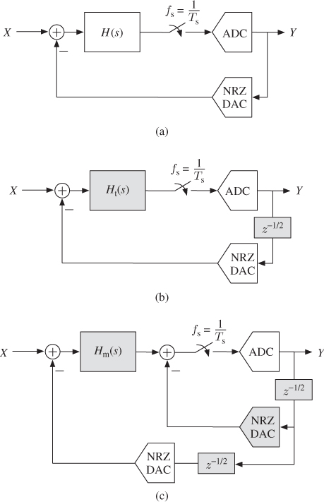
2.12 Finite Amplifier Gain in CT- Ms
Ms
Finite DC gain of amplifiers affects CT-![]() Ms exactly in the same way as shown in Section 2.2 for DT-
Ms exactly in the same way as shown in Section 2.2 for DT-![]() Ms. Let us consider an ideal active-RC integrator, in which the transfer function of the
Ms. Let us consider an ideal active-RC integrator, in which the transfer function of the ![]() th input path to the output is:
th input path to the output is:
2.72 ![]()
If the finite amplifier gain ![]() is accounted for in the CT integrator, as shown in Figure 2.31, the transfer function of the
is accounted for in the CT integrator, as shown in Figure 2.31, the transfer function of the ![]() th input path to the output can be derived as [2],
th input path to the output can be derived as [2],
2.73 
i.e., as a single-pole transfer function with a DC gain of ![]() and a pole at
and a pole at ![]() , which is displaced away from its ideal DC position.
, which is displaced away from its ideal DC position.
Figure 2.31 Active-RC integrator with ![]() input paths and finite amplifier gain
input paths and finite amplifier gain ![]() .
.

Assuming that ![]() for all integrators in the CT-
for all integrators in the CT-![]() M, the NTF degraded by finite amplifier gain can be derived following a procedure similar to that described in Section 2.2 for SC-
M, the NTF degraded by finite amplifier gain can be derived following a procedure similar to that described in Section 2.2 for SC-![]() Ms. The in-band noise of a second-order CT-
Ms. The in-band noise of a second-order CT-![]() M as that shown in Figure 1.36 can be thus obtained as [2],
M as that shown in Figure 1.36 can be thus obtained as [2],
2.74 ![]()
which matches Equation 2.7 for DT implementations taking into account that the DT–CT equivalence yields ![]() –see Equation 1.64.14
–see Equation 1.64.14
Similarly, the in-band noise of an Lth-order CT-![]() M with distributed feedback under the influence of leaky integrators yields [2],
M with distributed feedback under the influence of leaky integrators yields [2],
2.75 ![]()
which again matches Equation 2.9 if ![]() is accounted for in the DT–CT equivalence.
is accounted for in the DT–CT equivalence.
Finally, if a 2-1-1 cascade CT-![]() M is considered, the in-band noise under the influence of finite amplifier gain yields [2],
M is considered, the in-band noise under the influence of finite amplifier gain yields [2],
2.76 
which again matches Equation 2.10 of the equivalent SC-![]() M.
M.
Note that the conclusions derived in Section 2.2 for the influence of finite amplifier gain on the performance of DT-![]() Ms with either single-loop or cascade topologies are thus directly applicable to the CT case.
Ms with either single-loop or cascade topologies are thus directly applicable to the CT case.
2.13 Time-Constant Error in CT- Ms
Ms
As discussed in Section 2.3, deviations of the integrator gain coefficients from their nominal values due to variations in technological process parameters affect the performance of ![]() Ms differently depending on the modulator architecture. Single-loop topologies exhibit a quiet robust performance against integrator gain variations, whereas cascades suffer from the leakage of low-order-shaped quantization noise. However, the impact of this nonideality in SC-
Ms differently depending on the modulator architecture. Single-loop topologies exhibit a quiet robust performance against integrator gain variations, whereas cascades suffer from the leakage of low-order-shaped quantization noise. However, the impact of this nonideality in SC-![]() Ms is not critical, as integrator gains are implemented as capacitor ratios and thus make use of components with a matching better than
Ms is not critical, as integrator gains are implemented as capacitor ratios and thus make use of components with a matching better than ![]() in present CMOS processes.
in present CMOS processes.
Conversely, as shown in Section 1.8, integrator gains in CT-![]() Ms are mapped into
Ms are mapped into ![]() or
or ![]() values, involving thus absolute component values. Tolerances of
values, involving thus absolute component values. Tolerances of ![]() —
—![]() are not unusual in present CMOS technologies under process and temperature variations, which increases the possible variation of integrator gains to more than
are not unusual in present CMOS technologies under process and temperature variations, which increases the possible variation of integrator gains to more than ![]() [2]. Although the nature of the nonideality is essentially the same as for DT-
[2]. Although the nature of the nonideality is essentially the same as for DT-![]() Ms—that is, an integrator gain error—the magnitude of its impact can be clearly foreseen to be considerably larger on CT-
Ms—that is, an integrator gain error—the magnitude of its impact can be clearly foreseen to be considerably larger on CT-![]() Ms.
Ms.
If a tolerance ![]() is accounted for in the time constant of an active-RC integrator, the transfer function of the
is accounted for in the time constant of an active-RC integrator, the transfer function of the ![]() th input path to the output modifies to [2],
th input path to the output modifies to [2],
which can be used for recomputing the NTF and the IBN of a particular CT-![]() M architecture under the influence of this nonideality—assuming a modulator linear model.
M architecture under the influence of this nonideality—assuming a modulator linear model.
For an Lth-order CT-![]() M with distributed feedback, the IBN can be thus estimated as [2],
M with distributed feedback, the IBN can be thus estimated as [2],
where ![]() refers to the time-constant error of the
refers to the time-constant error of the ![]() th integrator. Note that the equation above is similar to Equation 2.13 for the influence of integrator gain errors in DT-
th integrator. Note that the equation above is similar to Equation 2.13 for the influence of integrator gain errors in DT-![]() Ms, taking into account that
Ms, taking into account that ![]() in the DT–CT equivalence.
in the DT–CT equivalence.
For a 2-1-1 CT cascade, the IBN under the influence of time-constant errors yields [2],

which is again similar to Equation 2.79 for the equivalent SC-![]() M.
M.
Figure 2.32 shows simulation results for the impact of time-constant errors on the performance of single-loop and cascade CT-![]() Ms, and compares them with the approximated expressions in Equations 2.78 and 2.79.15
Ms, and compares them with the approximated expressions in Equations 2.78 and 2.79.15
2.80 
where ![]() is the error in the last integrator gain. Note from the simulation results that single-loop modulators are affected by time-constant errors in two different ways:
is the error in the last integrator gain. Note from the simulation results that single-loop modulators are affected by time-constant errors in two different ways:
- For positive tolerances (
 ), the integrator gain coefficients
  in Equation 2.77 are reduced–or, similarly, coefficients
  in the equivalent DT-
 M. This leads only to less aggressive noise shapings and thus to an increase of the IBN.
 - For negative tolerances (
 ), integrator gain coefficients are increased, leading to more aggressive noise shapings. Therefore, after a short decrease of the IBN, negative time-constant errors reduce the modulator overload level and jeopardize its stability, as clearly visible for the third-order loop in Figure 2.32b.
The larger sensitivity of CT-![]() Ms to component tolerances is also noticeable from Figure 2.32c. Note that the IBN of the 2-1-1 cascade with
Ms to component tolerances is also noticeable from Figure 2.32c. Note that the IBN of the 2-1-1 cascade with ![]() increases nearly 30 dB for a time-constant error of
increases nearly 30 dB for a time-constant error of ![]() .
.
Figure 2.32 Simulation results for the in-band noise of CT-![]() Ms under the influence of time-constant errors: (a) second-order single-loop, (b) third-order single-loop and (c) 2-1-1 cascade. Simulation results have been obtained for an input signal with
Ms under the influence of time-constant errors: (a) second-order single-loop, (b) third-order single-loop and (c) 2-1-1 cascade. Simulation results have been obtained for an input signal with ![]() and
and ![]() and for an NRZ rectangular feedback. Approximated results have been obtained from Equations 2.78 and 2.79.
and for an NRZ rectangular feedback. Approximated results have been obtained from Equations 2.78 and 2.79.

Concluding, the design of high-order single-loop CT-![]() Ms is in practice more limited by their tendency to instability (for
Ms is in practice more limited by their tendency to instability (for ![]() ) than by the degradation of the IBN (for
) than by the degradation of the IBN (for ![]() ). Therefore, if no countermeasures are taken against the influence of gain errors, less aggressive noise shapings must be implemented using a set of scaling coefficients that are nonoptimal in terms of the modulator performance, but for which stability can be guaranteed over all the
). Therefore, if no countermeasures are taken against the influence of gain errors, less aggressive noise shapings must be implemented using a set of scaling coefficients that are nonoptimal in terms of the modulator performance, but for which stability can be guaranteed over all the ![]() possible variations [36, 37].
possible variations [36, 37].
Alternatively, time-constant errors can be reduced in CT-![]() Ms by tuning the absolute value of passive components with programmable banks of capacitors [30] or resistors [38].16
Ms by tuning the absolute value of passive components with programmable banks of capacitors [30] or resistors [38].16
Conversely to tuning the analog filter, cascade architectures also offer the possibility of digitally correcting the error cancelation logic to reduce the power of low-order-shaped quantization noise that leaks to the modulator output [39]. Digital correction techniques have been successfully used for reducing the impact of time-constant errors in CT-![]() Ms [40, 41].
Ms [40, 41].
2.14 Finite Integrator Dynamics in CT- Ms
Ms
The influence of finite amplifier GB can be easily incorporated into CT modulators by replacing the amplifier in Figure 2.31 by a single-pole model,
where ![]() is the dominant pole of the amplifier inside the integrator. The integrator transfer function of the
is the dominant pole of the amplifier inside the integrator. The integrator transfer function of the ![]() th input path to the output is thus modified to [2],
th input path to the output is thus modified to [2],
2.82 
where an integrator gain error arises due to the finite amplifier GB, as well as a second pole. For the sake of clarity, the modified ITF can thus be rewritten as,

where ![]() .
.
Regarding Equation 2.83, the influence of the second integrator pole is often neglected to derive closed-form expressions for the influence of finite amplifier GB on CT-![]() Ms. In that case, the expressions for the IBN due to finite GB can be approximated from the corresponding expressions for the gain error introduced by time-constant variations—Equations 2.78 and 2.79—just by replacing
Ms. In that case, the expressions for the IBN due to finite GB can be approximated from the corresponding expressions for the gain error introduced by time-constant variations—Equations 2.78 and 2.79—just by replacing ![]() with the expression for
with the expression for ![]() in Equation 2.83. The observations already made in Section 2.13 on the different sensitivity of single-loop and cascade architectures and on possible correction techniques also apply here.
in Equation 2.83. The observations already made in Section 2.13 on the different sensitivity of single-loop and cascade architectures and on possible correction techniques also apply here.
The former approximation can a priori be considered too coarse, but it provides results that are in accordance to the simulation of NRZ CT-![]() Ms if the amplifier GB is not very low (
Ms if the amplifier GB is not very low (![]() ) [2].
) [2].
However, finite amplifier GB is a typical nonideality concerning the dynamics of a ![]() M and, as such, by changing the shape and the dynamic behavior of the feedback pulses, its influence on the modulator performance is expected to change [2]. Conversely, not much published work exists that extends the basic single-pole model in Equation 2.81 and/or applies it to different feedback pulse forms [42]. Even less literature exists for the influence of the finite amplifier SR on the performance of CT-
M and, as such, by changing the shape and the dynamic behavior of the feedback pulses, its influence on the modulator performance is expected to change [2]. Conversely, not much published work exists that extends the basic single-pole model in Equation 2.81 and/or applies it to different feedback pulse forms [42]. Even less literature exists for the influence of the finite amplifier SR on the performance of CT-![]() Ms and most designs strongly rely on simulations. The reason for that may be found in the fact that, generally speaking, CT-
Ms and most designs strongly rely on simulations. The reason for that may be found in the fact that, generally speaking, CT-![]() Ms can work with a finite amplifier GB and SR in the integrators lower than SC implementations (see Section 2.4.2 and 2.4.3), due to the lack of high-current peaks of the latter.
Ms can work with a finite amplifier GB and SR in the integrators lower than SC implementations (see Section 2.4.2 and 2.4.3), due to the lack of high-current peaks of the latter.
2.15 Circuit Noise in CT- Ms
Ms
As discussed in Section 2.5, circuit noise strongly impacts the in-band noise of SC-![]() Ms due to the aliasing of broadband noise components that are sampled together with the modulator input signal. Conversely, sampling capacitors are not used in purely CT-
Ms due to the aliasing of broadband noise components that are sampled together with the modulator input signal. Conversely, sampling capacitors are not used in purely CT-![]() Ms, so that
Ms, so that ![]() noise is not present, which is a clear advantage. Broadband noise components are thus filtered before they get to the sampler, so that the foldover effect is attenuated by the modulator noise shaping [2].
noise is not present, which is a clear advantage. Broadband noise components are thus filtered before they get to the sampler, so that the foldover effect is attenuated by the modulator noise shaping [2].
Let us consider the active-RC integrator in Figure 2.33 to be the front-end integrator of a CT-![]() M. Two input branches are considered: one for the modulator input signal (
M. Two input branches are considered: one for the modulator input signal (![]() ) and the other for the DAC feedback signal (
) and the other for the DAC feedback signal (![]() ). Resistors thermal noise and amplifier noise have been incorporated to the scheme in Figure 2.33.17 On the one hand, each resistor has a noise voltage source
). Resistors thermal noise and amplifier noise have been incorporated to the scheme in Figure 2.33.17 On the one hand, each resistor has a noise voltage source ![]() in series, whose PSD in a single-sided representation is thus
in series, whose PSD in a single-sided representation is thus
where ![]() is Boltzmann's constant and
is Boltzmann's constant and ![]() is the absolute temperature. On the other hand, the voltage source
is the absolute temperature. On the other hand, the voltage source ![]() represents the amplifier input noise. As illustrated in Figure 2.16, it is basically determined by a broadband thermal component and a narrowband
represents the amplifier input noise. As illustrated in Figure 2.16, it is basically determined by a broadband thermal component and a narrowband ![]() component, so that
component, so that ![]() is given by Equation 2.36.
is given by Equation 2.36.
Figure 2.33 Circuit noise sources in a CT active-RC integrator with two input paths. Single-ended version.

Adding up the former circuit noise components in the CT integrator, the total input-referred noise PSD yields [25, 26]

where the factor 2 before the brackets accounts for the actual fully-differential implementation of the CT integrator, in which the number of resistors doubles compared with the single-ended scheme in Figure 2.33. Replacing Equations 2.84 and 2.36 in 2.85, the total input-referred noise PSD of the front-end integrator of the CT-![]() M can thus be approximated to:
M can thus be approximated to:
2.86 
The input-referred IBN of a CT-![]() M due to circuit noise can be easily obtained by integrating the former equation over the input signal bandwidth, yielding
M due to circuit noise can be easily obtained by integrating the former equation over the input signal bandwidth, yielding

in which the ![]() noise component has been integrated from a frequency
noise component has been integrated from a frequency ![]() toexclude DC. Taking into account that
toexclude DC. Taking into account that ![]() , resulting terms that are proportional to
, resulting terms that are proportional to ![]() have been neglected in the final calculation [2].
have been neglected in the final calculation [2].
For a CT-![]() M to achieve a given noise performance, the sum of all three components in Equation 2.87 have to meet the demanded noise floor. Note that, to reduce the contribution of the resistors' thermal noise, the integrator resistance at the modulator input must be decreased, which results in a larger power consumption, given that
M to achieve a given noise performance, the sum of all three components in Equation 2.87 have to meet the demanded noise floor. Note that, to reduce the contribution of the resistors' thermal noise, the integrator resistance at the modulator input must be decreased, which results in a larger power consumption, given that ![]() . To reduce the amplifier noise, its transconductance can be increased (for the white noise component) and the size of the input transistors can be increased (for the flicker component).
. To reduce the amplifier noise, its transconductance can be increased (for the white noise component) and the size of the input transistors can be increased (for the flicker component).
2.16 Sources of Distortion in CT- Ms
Ms
The linearity of a CT-![]() M is ultimately limited by that of the input stage and by signal-dependent errors arising from the feedback DAC. Both sources of distortion are briefly discussed next.
M is ultimately limited by that of the input stage and by signal-dependent errors arising from the feedback DAC. Both sources of distortion are briefly discussed next.
2.16.1 Nonlinearities in the Front-End Integrator
As stated in Section 2.7>, the linearity of a ![]() modulator is ultimately limited by the nonlinearities associated with the first integrator. Therefore, for medium- and high-resolution CT-
modulator is ultimately limited by the nonlinearities associated with the first integrator. Therefore, for medium- and high-resolution CT-![]() Ms, active-RC integrators are usually employed at the modulator front end rather than Gm-C integrators [2, 25, 43], because a more linear voltage-to-current conversion can be obtained in practice with resistors than with active devices.
Ms, active-RC integrators are usually employed at the modulator front end rather than Gm-C integrators [2, 25, 43], because a more linear voltage-to-current conversion can be obtained in practice with resistors than with active devices.
Similarly as done in Figure 2.18 for SC implementations, Figure 2.34 illustrates the main sources of distortion in an active-RC integrator, in which the amplifier usually plays the dominant role, due to the high linearity achieved by passive devices in present mixed-mode technological processes. On the contrary, the DC gain of an amplifier exhibits in practice a high dependency on the common-mode output voltage due to degradation of its output impedance, as illustrated in Figure 2.19. Moreover, nonlinearities in the differential input pair of the amplifier are accentuated by the finite DC gain. In [43] it is shown how a small residue differential voltage at the input pair due to finite gain is modulated and the third-order harmonic distortion is derived as
2.88 ![]()
where ![]() is the input resistor,
is the input resistor, ![]() is the feedback resistor, and
is the feedback resistor, and ![]() and
and ![]() are, respectively, the transconductance and the bias current of the input transistors of the amplifier. Note from the equation earlier that the modulator linearity can be considerably improved by increasing
are, respectively, the transconductance and the bias current of the input transistors of the amplifier. Note from the equation earlier that the modulator linearity can be considerably improved by increasing ![]() as much as the thermal noise limit allows–see Equation 2.87. Although with lower efficiency, a larger amplifier input transconductance also benefits linearity and at the same time helps to reduce thermal noise.
as much as the thermal noise limit allows–see Equation 2.87. Although with lower efficiency, a larger amplifier input transconductance also benefits linearity and at the same time helps to reduce thermal noise.
Figure 2.34 Main sources of distortion in a fully-differential active-RC integrator.

2.16.2 Intersymbol Interference in the Feedback DAC
In practical realizations of CT-![]() Ms, besides timing errors due to emerging excess loop delay (see Section 2.10) and nonlinearities arising from mismatches between the output levels of multibit DACs (see Section 1.6), the implemented feedback DAC also exhibits SR limitations as well as different rise and fall times. These nonidealities cause additional errors that directly add to the modulator input and tend to degrade the performance, unless they are made small enough.
Ms, besides timing errors due to emerging excess loop delay (see Section 2.10) and nonlinearities arising from mismatches between the output levels of multibit DACs (see Section 1.6), the implemented feedback DAC also exhibits SR limitations as well as different rise and fall times. These nonidealities cause additional errors that directly add to the modulator input and tend to degrade the performance, unless they are made small enough.
For the case of CT-![]() Ms employing an NRZ-DAC, these nonidealities introduce intersymbol interference (ISI) [44], as illustrated in Figure 2.35a. Note that any limitation on the DAC SR or mismatch between its rise and fall times makes the area of one 1-symbol differ from half of the area of two consecutive 1-symbols. Therefore, the resulting errors in the feedback charge depend on the modulator output sequence and thus create a signal-dependent distortion that limits the modulator performance.
Ms employing an NRZ-DAC, these nonidealities introduce intersymbol interference (ISI) [44], as illustrated in Figure 2.35a. Note that any limitation on the DAC SR or mismatch between its rise and fall times makes the area of one 1-symbol differ from half of the area of two consecutive 1-symbols. Therefore, the resulting errors in the feedback charge depend on the modulator output sequence and thus create a signal-dependent distortion that limits the modulator performance.
Figure 2.35 Influence of the DAC slew rate limitation on the feedback charge for: (a) NRZ DAC, causing a signal-dependent charge error (ISI) and (b) RZ DAC, causing a constant charge error.

The most common solution to avoid ISI is to resort to RZ feedback pulses, so that, in spite of different rise and fall times in the DAC response, the error remains constant in every clock period and independent of the output sequence, as shown in Figure 2.35b. This way, the resulting error can be compensated by tuning the modulator scaling coefficients [2], similarly to the compensation of pure ELD already discussed in Section 2.10.
2.17 Case Study: High-Level Sizing of a  M
M
For the sake of illustration, this section provides guidelines on how to face the design of a ![]() modulator to fulfill a given set of specifications by means of the closed-form expressions and the behavioral models previously derived in the chapter. The impact of the different circuit nonidealities on the
modulator to fulfill a given set of specifications by means of the closed-form expressions and the behavioral models previously derived in the chapter. The impact of the different circuit nonidealities on the ![]() M performance will be considered in a cumulative way, trying to map the modulator specifications onto the electrical requirements of its main building blocks in a top-down design methodology–often referred to as the high-level sizing of a
M performance will be considered in a cumulative way, trying to map the modulator specifications onto the electrical requirements of its main building blocks in a top-down design methodology–often referred to as the high-level sizing of a ![]() M.
M.
This approach will be exemplified on a 2-1-1 cascade SC-![]() M operating at 100-MHz clock frequency intended to achieve an effective resolution of around 12bit in the A/D conversion of low-pass signals with 4-MHz bandwidth. To that purpose, let us consider the Z-domain block diagram of a 2-1-1 DT cascade illustrated in Figure 1.23, together with the modulator scaling coefficients in the first column of Table 1.2 [6]. Let us also assume a modulator full-scale range of 2V.
M operating at 100-MHz clock frequency intended to achieve an effective resolution of around 12bit in the A/D conversion of low-pass signals with 4-MHz bandwidth. To that purpose, let us consider the Z-domain block diagram of a 2-1-1 DT cascade illustrated in Figure 1.23, together with the modulator scaling coefficients in the first column of Table 1.2 [6]. Let us also assume a modulator full-scale range of 2V.
2.17.1 Ideal Modulator Performance
The ideal in-band quantization error of the 2-1-1 cascade ![]() M can be particularized from Equation 1.44 to:
M can be particularized from Equation 1.44 to:
If single-bit quantization is used in the three cascaded stages (![]() ), Equation 2.89 yields an
), Equation 2.89 yields an ![]() of
of ![]() for
for ![]() (as
(as ![]() ) and
) and ![]() (as
(as ![]() and
and![]() . Therefore, an oversampling ratio of 12.5 is clearly insufficient only in combination with a fourth-order shaping for the cascade to achieve the required IBN; e.g.,
. Therefore, an oversampling ratio of 12.5 is clearly insufficient only in combination with a fourth-order shaping for the cascade to achieve the required IBN; e.g., ![]() for a 13-bit ENOB, as obtained from Equations 1.19 and 1.20.
for a 13-bit ENOB, as obtained from Equations 1.19 and 1.20.
Taking advantage of the easiness to employ dual-quantization schemes in cascade ![]() Ms (see Section 1.6.3),
Ms (see Section 1.6.3), ![]() can be easily reduced by resorting to a multibit quantizer in the last stage. For
can be easily reduced by resorting to a multibit quantizer in the last stage. For ![]() , the last-stage quantization step reduces to
, the last-stage quantization step reduces to ![]() and
and ![]() thus yields
thus yields ![]() . Figure 2.36 illustrates the spectra of the
. Figure 2.36 illustrates the spectra of the ![]() cascade for an input sinusoid of
cascade for an input sinusoid of ![]() at
at ![]() (
(![]() ). The figure compares the spectrum of the overall output of the fourth-order multibit cascade (labeled as 211mb) with those of its partial second- and third-order single-bit outputs (labelled as SL2 and 21, respectively). The increase in the shaping order is evident from the slopes of the spectra, whereas the reduction of the quantization error power for the multibit case is noticeable at the high-frequency region.
). The figure compares the spectrum of the overall output of the fourth-order multibit cascade (labeled as 211mb) with those of its partial second- and third-order single-bit outputs (labelled as SL2 and 21, respectively). The increase in the shaping order is evident from the slopes of the spectra, whereas the reduction of the quantization error power for the multibit case is noticeable at the high-frequency region.
Figure 2.36 Illustration of the second-, third-, and fourth-order shaping in the 2-1-1 ![]() M. Quantization noise in the three
M. Quantization noise in the three ![]() stages is considered as the only source of error. Input signal with
stages is considered as the only source of error. Input signal with ![]() and
and ![]() .
.

Figure 2.37 illustrates a possible implementation of the 2-1-1 multibit ![]() M using fully-differential SC techniques. Note that only the mixed-signal section of the cascade is shown, whereas the required digital filtering to combine the stage outputs (
M using fully-differential SC techniques. Note that only the mixed-signal section of the cascade is shown, whereas the required digital filtering to combine the stage outputs (![]() ,
, ![]() , and
, and ![]() ) and to ideally cancel the lower-order quantization errors is omitted–see Figure 1.23. Note also that the stages would operate with a differential reference voltage
) and to ideally cancel the lower-order quantization errors is omitted–see Figure 1.23. Note also that the stages would operate with a differential reference voltage ![]() to obtain the 2-V differential full-scale range. The values of the sampling and integrating capacitors in Figure 2.37 are expressed as multiples of a unit capacitor
to obtain the 2-V differential full-scale range. The values of the sampling and integrating capacitors in Figure 2.37 are expressed as multiples of a unit capacitor ![]() , whose ratios implement the modulator scaling coefficients in the first column of Table 1.2 [6]. To adapt them to the multibit quantization in the last stage, the corresponding coefficients are doubled (
, whose ratios implement the modulator scaling coefficients in the first column of Table 1.2 [6]. To adapt them to the multibit quantization in the last stage, the corresponding coefficients are doubled (![]() ,
, ![]() in the multibit case).
in the multibit case).
Figure 2.37 Fully-differential SC implementation of the 2-1-1 multibit ![]() modulator.
modulator.
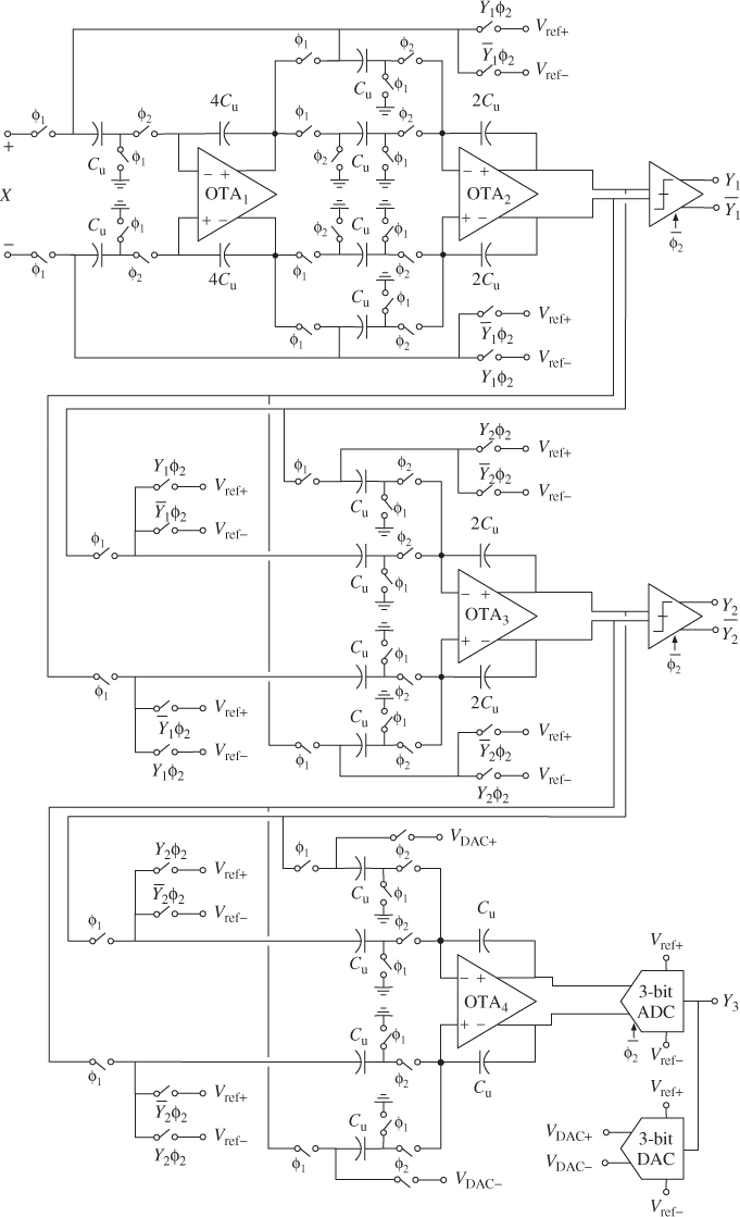
2.17.2 Noise Leakages
As discussed in Section 1.6.1, errors in the multibit DAC will be mostly determined by the mismatching between its unit elements, which would be resistors for the SC-![]() M in Figure 2.37. From Equation 1.48 worst-case errors in the 3-bit DAC output can be estimated as,
M in Figure 2.37. From Equation 1.48 worst-case errors in the 3-bit DAC output can be estimated as,
2.90 ![]()
where ![]() represents the relative error in the value of the unit resistor and three sigmas are considered. Thanks to the dual-quantization scheme these errors are injected at the last-stage input and will be third-order shaped at the modulator output, so that their contribution to the total IBN can be estimated from Equation 1.50 as:
represents the relative error in the value of the unit resistor and three sigmas are considered. Thanks to the dual-quantization scheme these errors are injected at the last-stage input and will be third-order shaped at the modulator output, so that their contribution to the total IBN can be estimated from Equation 1.50 as:
Assuming a standard deviation of 0.1% in the unit resistors–which is a reasonable value in present-day mixed-signal CMOS processes–![]() equals
equals ![]() ; that is, it is negligible compared with
; that is, it is negligible compared with ![]() .
.
As discussed throughout this chapter, cascade ![]() Ms are especially sensitive to leakages of low-order quantization errors due to circuit-level nonidealities. For the case of SC
Ms are especially sensitive to leakages of low-order quantization errors due to circuit-level nonidealities. For the case of SC ![]() cascades, the most critical error mechanisms are the finite gain of the amplifiers and the mismatching between the unit capacitors used for implementing the modulator coefficients. Figure 2.38 illustrates the impact of noise leakages on the output spectrum of the 2-1-1 multibit
cascades, the most critical error mechanisms are the finite gain of the amplifiers and the mismatching between the unit capacitors used for implementing the modulator coefficients. Figure 2.38 illustrates the impact of noise leakages on the output spectrum of the 2-1-1 multibit ![]() M for a DC gain of 65 dB in the amplifiers and a capacitor mismatch of 0.1%, in addition to the multibit DAC errors. Results are compared with a purely ideal behavioral simulation only considering quantization errors (as done in Figure 2.36). The integrated error powers versus frequency are also included for comparison purposes. Note that, in spite of the degradation of the ideal shaping performance due to noise leakages, the resulting error power integrated in the 4-MHz bandwidth (
M for a DC gain of 65 dB in the amplifiers and a capacitor mismatch of 0.1%, in addition to the multibit DAC errors. Results are compared with a purely ideal behavioral simulation only considering quantization errors (as done in Figure 2.36). The integrated error powers versus frequency are also included for comparison purposes. Note that, in spite of the degradation of the ideal shaping performance due to noise leakages, the resulting error power integrated in the 4-MHz bandwidth (![]() ) is only slightly larger than the simulated
) is only slightly larger than the simulated ![]() (
(![]() ). The influence of both error mechanisms can be separately estimated from Equations 1.19 and 1.20 as:
). The influence of both error mechanisms can be separately estimated from Equations 1.19 and 1.20 as:
The increase in the modulator IBN due to integrator leakages can thus be estimated as ![]() for
for ![]() , whereas that due to capacitor mismatch equals
, whereas that due to capacitor mismatch equals ![]() for
for ![]() .18
.18
Figure 2.38 Effect of noise leakages on the modulator output spectrum (![]() ,
, ![]() ,
, ![]() ). Input signal with
). Input signal with ![]() and
and ![]() .
.
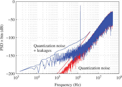
The former equations can also be employed to evaluate the influence of noise leakages on the performance of the 2-1-1 ![]() M under different clock rates and multibit quantizations. This is illustrated in Figure 2.39, which shows the effective resolution of the
M under different clock rates and multibit quantizations. This is illustrated in Figure 2.39, which shows the effective resolution of the ![]() cascade against
cascade against ![]() for varying OSR. Note that the ENOB curves tend to saturate in the presence of nonidealities, leading to a practical useful limit of multibit quantization. However, for the values assumed for the nonideal parameters
for varying OSR. Note that the ENOB curves tend to saturate in the presence of nonidealities, leading to a practical useful limit of multibit quantization. However, for the values assumed for the nonideal parameters ![]() ,
, ![]() , and
, and ![]() , the initial selection of
, the initial selection of ![]() for
for ![]() provides a good trade-off for achieving the targeted modulator performance.19
provides a good trade-off for achieving the targeted modulator performance.19
Figure 2.39 Modulator effective resolution versus the number of bits in the last-stage quantizer for varying OSR. All noise leakages are considered (![]() ,
, ![]() ,
, ![]() ).
).

2.17.3 Circuit Noise
As discussed in Section 1.6.1, the contribution of circuit noise to the overall IBN is dominated by the front-end integrator. Only ![]() noise and amplifier thermal noise will be considered in this high-level sizing of the 2-1-1 SC-
noise and amplifier thermal noise will be considered in this high-level sizing of the 2-1-1 SC-![]() M.
M.
On the one hand, the ![]() noise budget determines the minimum value of the sampling capacitor (
noise budget determines the minimum value of the sampling capacitor (![]() ) to be used. A small value will be selected to reduce the capacitive load of the integrators and, hence, their settling requirements. This noise contribution can be estimated from Equation 2.40 as:
) to be used. A small value will be selected to reduce the capacitive load of the integrators and, hence, their settling requirements. This noise contribution can be estimated from Equation 2.40 as:
2.94 ![]()
For ![]() in the front-end integrator (Figure 2.37),
in the front-end integrator (Figure 2.37), ![]() equals
equals ![]() ; that is, it yields an in-band contribution similar to that of the ideal quantization noise.20
; that is, it yields an in-band contribution similar to that of the ideal quantization noise.20
On the other hand, the contribution of the amplifier thermal noise can be estimated from Equation 2.40 as,
2.95 ![]()
which requires knowing a priori the amplifier gain-bandwidth product to quantify the foldover effect. The required ![]() can be estimated by means of considering the integrator settling error as a linear gain error, as discussed in Section 2.4.2. Therefore, the in-band noise due to limited linear dynamics21 can be obtained similarly to Equation 2.96 as,
can be estimated by means of considering the integrator settling error as a linear gain error, as discussed in Section 2.4.2. Therefore, the in-band noise due to limited linear dynamics21 can be obtained similarly to Equation 2.96 as,
where ![]() represents the gain error, given by:
represents the gain error, given by:
2.97 ![]()
For ![]() (around 200 MHz),
(around 200 MHz), ![]() equals
equals ![]() . This value is considerably smaller than
. This value is considerably smaller than ![]() and
and ![]() to have some margin in the noise budget for allocating more accurate settling error estimations in the next steps.
to have some margin in the noise budget for allocating more accurate settling error estimations in the next steps.
Based on this value of ![]() for settling considerations, the input-referred thermal noise of the amplifier can be estimated for a given noise budget. For
for settling considerations, the input-referred thermal noise of the amplifier can be estimated for a given noise budget. For ![]() ,
, ![]() equals
equals ![]() . The total in-band white noise will be thus dominated by
. The total in-band white noise will be thus dominated by ![]() noise and can be obtained to equal
noise and can be obtained to equal ![]() .
.
2.17.4 Settling Error
Assuming that the parasitics at the amplifier input and output nodes are ![]() and
and ![]() respectively, the equivalent load at the amplifier output during integration can be obtained from Equation 2.16
respectively, the equivalent load at the amplifier output during integration can be obtained from Equation 2.16
2.98 ![]()
to be around 1.2pF. Formerly, the required amplifier GB was estimated considering only a linear settling error to be ![]() . According to Equation 2.27, the amplifier transconductance for a dominant-pole model yields around 1.5mA/V.
. According to Equation 2.27, the amplifier transconductance for a dominant-pole model yields around 1.5mA/V.
Figure 2.40 shows simulation results for the considered 2-1-1 ![]() M using the behavioral model for the transient response of SC integrators presented in Section 2.4.1, which accurately accounts for both linear and nonlinear integrator dynamics. The simulated modulator IBN against the amplifier transconductance is shown in Figure 2.40a for different values of the amplifier output current. Note that, for
M using the behavioral model for the transient response of SC integrators presented in Section 2.4.1, which accurately accounts for both linear and nonlinear integrator dynamics. The simulated modulator IBN against the amplifier transconductance is shown in Figure 2.40a for different values of the amplifier output current. Note that, for ![]() , the modulator performance is not limited by nonlinear integrator dynamics as long as
, the modulator performance is not limited by nonlinear integrator dynamics as long as ![]() . According to Equation 2.27, the required amplifier SR can be estimated as
. According to Equation 2.27, the required amplifier SR can be estimated as
2.99 ![]()
to be around ![]() .
.
Figure 2.40 Influence of the amplifier dynamics on the modulator performance: (a) IBN against the amplifier transconductance for different values of the amplifier output current and (b) output spectrum for ![]() and different amplifier output currents. Input signal with
and different amplifier output currents. Input signal with ![]() and
and ![]() . Noise leakages and thermal noise are also accounted for in the behavioral simulations.
. Noise leakages and thermal noise are also accounted for in the behavioral simulations.

Figure 2.40b illustrates the effect of the amplifier limited output current on the modulator output spectra for a ![]() @
@![]() input tone. Note that, for
input tone. Note that, for ![]() , the limited amplifier SR clearly degrades the shaping performance of the modulator.
, the limited amplifier SR clearly degrades the shaping performance of the modulator.
2.17.5 Overall High-Level Sizing and Noise Budget
Table 2.1 summarizes the electrical specifications of the main modulator blocks derived in the presented high-level sizing of the 2-1-1 SC-![]() M. Accordingly, Table 2.2 shows the selected noise budget for achieving the targeted resolution of 12 bit at 4-MHz conversion bandwidth. According to the closed-form expressions used, the total in-band noise is
M. Accordingly, Table 2.2 shows the selected noise budget for achieving the targeted resolution of 12 bit at 4-MHz conversion bandwidth. According to the closed-form expressions used, the total in-band noise is ![]() , leading to a DR of 77.1 dB (12.5 bit).
, leading to a DR of 77.1 dB (12.5 bit).
Table 2.1 High-level sizing of the 2-1-1 SC-![]() M
M
| Modulator | Topology | 2-1-1 |
| Dual quantization, |
||
| Signal bandwidth, |
||
| Clock frequency, |
||
| Oversampling ratio, OSR | ||
| Reference voltage, |
||
| Front-end integrator | Unit capacitor, |
|
| Capacitor standard deviation, |
||
| Sampling capacitor, |
||
| Integration capacitor, |
||
| Front-end amplifier | DC gain, |
|
| Input capacitor, |
||
| Output capacitor, |
||
| Equivalent output load, |
||
| Transconductance, |
||
| Gain-bandwidth product, |
||
| Slew rate, |
||
| Input-referred thermal noise, |
||
| Output swing | ||
| Last-stage quantizer | Resistor standard deviation, |
Table 2.2 Noise budget for the high-level sizing of the 2-1-1 SC-![]() M proposed in Table 2.1
M proposed in Table 2.1

Note from Table 2.1 that the derived requirements apply for the front-end integrator, whereas those of the remaining integrators can be usually scaled down to some extent. Extensive behavioral simulations are often performed for this purpose.
Note also that the generated distortion has not been strictly evaluated, so that the derived values for the gain and SR of the front-end amplifier may increase depending on the involved nonlinearities not to degrade the modulator SNDR.
However, the requirements obtained for the modulator blocks can be used as the starting point for their electrical design. A bottom-up approach is then often followed to ensure the fulfillment of the targeted modulator specifications.
2.18 Summary
In this chapter, the main error mechanisms degrading the performance of SC- and CT-![]() Ms have been analyzed. These errors are caused by nonidealities affecting the circuit implementation of the modulator analog blocks and produce extra error components that add to the in-band quantization error noise that can severely limit the modulator performance. Therefore, nonidealities have been studied in detail and behavioral models and, if possible, practical closed-form expressions have been presented to estimate their influence on the
Ms have been analyzed. These errors are caused by nonidealities affecting the circuit implementation of the modulator analog blocks and produce extra error components that add to the in-band quantization error noise that can severely limit the modulator performance. Therefore, nonidealities have been studied in detail and behavioral models and, if possible, practical closed-form expressions have been presented to estimate their influence on the ![]() M behavior.
M behavior.
Errors modifying the noise transfer function of the ![]() M have been analyzed, such as the finite amplifier gain, capacitor mismatch, and integrator settling for SC-
M have been analyzed, such as the finite amplifier gain, capacitor mismatch, and integrator settling for SC-![]() Ms, and excess loop delay and time-constant error for CT-
Ms, and excess loop delay and time-constant error for CT-![]() Ms. As shown, single-loop modulator topologies are less sensitive to these errors than cascades, which suffer from noise leakage.
Ms. As shown, single-loop modulator topologies are less sensitive to these errors than cascades, which suffer from noise leakage.
Nonidealities whose effect can be modeled as an additive noise source at the modulator input have been studied, such as circuit noise and clock jitter in both SC- and CT-![]() Ms. The main sources of distortion in both types of modulator implementation have also been addressed.
Ms. The main sources of distortion in both types of modulator implementation have also been addressed.
References
[1] S. R. Norsworthy, R. Schreier, and G. C. Temes, Delta-Sigma Data Converters: Theory, Design and Simulation, IEEE Press, 1997.
[2] M. Ortmanns and F. Gerfers, Continuous-Time Sigma-Delta A/D Conversion: Fundamentals, Performance Limits and Robust Implementations, Springer, 2006.
[3] R. del Río, F. Medeiro, B. Pérez-Verdú, J. M. de la Rosa, and A. Rodríguez-Vázquez, CMOS Cascade ![]() Modulators for Sensors and Telecom: Error Analysis and Practical Design, Springer, 2006.
Modulators for Sensors and Telecom: Error Analysis and Practical Design, Springer, 2006.
[4] A. Marques, V. Peluso, M. S. Steyaert, and W. M. Sansen, “Optimal Parameters for ![]() Modulator Topologies,” IEEE Transactions on Circuits and Systems II: Analog and Digital Signal Processing, vol. 45, pp. 1232–1241, September 1998.
Modulator Topologies,” IEEE Transactions on Circuits and Systems II: Analog and Digital Signal Processing, vol. 45, pp. 1232–1241, September 1998.
[5] Y. Geerts, M. Steyaert, and W. Sansen, Design of Multi-bit Delta-Sigma A/D Converters, Kluwer Academic Publishers, 2002.
[6] R. del Río, F. Medeiro, J. M. de la Rosa, B. Pérez-Verdú, and A. Rodríguez-Vázquez, “Reliable Analysis of Settling Errors in SC Integrators: Application to ![]() Modulators,” IET Electronics Letters, vol. 36, pp. 503–504, March 2000.
Modulators,” IET Electronics Letters, vol. 36, pp. 503–504, March 2000.
[7] J. Fischer, “Noise Sources and Calculation Techniques for Switched Capacitor Filters,” IEEE Journal of Solid-State Circuits, vol. 17, pp. 742–752, August 1982.
[8] C.-A. Gobet and A. Knob, “Noise Analysis of Switched Capacitor Networks,” IEEE Transactions on Circuits and Systems, vol. CAS-30, pp. 37–43, January 1983.
[9] R. Gregorian and G. C. Temes, Analog MOS Integrated Circuits for Signal Processing, John Wiley & Sons, 1986.
[10] C. C. Enz and G. C. Temes, “Circuit Techniques for Reducing the Effects of Op-Amp Imperfections: Autozeroing, Correlated Double Sampling, and Chopper Stabilization,” Proceedings of the IEEE, vol. 84, pp. 1584–1614, November 1996.
[11] T. H. Lee, The Design of CMOS Radio-Frequency Integrated Circuits, Cambridge University Press, 2004.
[12] B. E. Boser and B. A. Wooley, “The Design of Sigma-Delta Modulation Analog-to-Digital Converters,” IEEE Journal of Solid-State Circuits, vol. 23, pp. 1298–1308, December 1988.
[13] B. Brandt, P. Ferguson, and M. Rebeschini, “Analog Circuit Design of ![]() ADCs,” Chapter 11 in Delta-Sigma Data Converters: Theory, Design and Simulation (S. R. Norsworthy, R. Schreier, and G. C. Temes, Editors), IEEE Press, 1997.
ADCs,” Chapter 11 in Delta-Sigma Data Converters: Theory, Design and Simulation (S. R. Norsworthy, R. Schreier, and G. C. Temes, Editors), IEEE Press, 1997.
[14] D. Haigh and B. Singh, “A Switching Scheme for Switched Capacitor Filters which Reduces the Effect of Parasitic Capacitances Associated with Switch Control Terminals,” Proc. of the IEEE Intl. Symp. on Circuits and Systems, pp. 586–589, 1983.
[15] G. Yin and W. Sansen, “A High-Frequency and High-Resolution Fourth-Order ![]() A/D Converter in BiCMOS Technology,” IEEE Journal of Solid-State Circuits, vol. 29, pp. 857–865, August 1994.
A/D Converter in BiCMOS Technology,” IEEE Journal of Solid-State Circuits, vol. 29, pp. 857–865, August 1994.
[16] K. R. Laker and W. M. C. Sansen, Design of Analog Integrated Circuits and Systems, McGraw-Hill, 1994.
[17] J.-T. Wu and K.-L. Chang, “MOS Charge Pumps for Low-Voltage Operation,” IEEE Journal of Solid-State Circuits, vol. 33, pp. 592–597, April 1998.
[18] K. Bult, “Analog Design in Deep Sub-Micron CMOS,” Proc. of the IEEE European Solid-State Circuits Conf., pp. 11–17, 2000.
[19] J. Cherry and W. Snelgrove, “Clock Jitter and Quantizer Metastability in Continuous-Time Delta–Sigma Modulators,” IEEE Transactions on Circuits and Systems—II: Analog and Digital Signal Processing, vol. 46, pp. 661–676, June 1999.
[20] S. Luschas and H. S. Lee, “High-Speed ![]() Modulators with Reduced Timing Jitter Sensitivity,” IEEE Transactions on Circuits and Systems—II: Analog and Digital Signal Processing, vol. 49, pp. 712–720, November 2002.
Modulators with Reduced Timing Jitter Sensitivity,” IEEE Transactions on Circuits and Systems—II: Analog and Digital Signal Processing, vol. 49, pp. 712–720, November 2002.
[21] O. Oliaei, “Design of Continuous-Time Sigma-Delta Modulators with Arbitrary Feedback Waveform,” IEEE Transactions on Circuits and Systems—II: Analog and Digital Signal Processing, vol. 50, pp. 437–444, August 2003.
[22] O. Oliaei, “Sigma-Delta Modulator with Spectrally Shaped Feedback,” IEEE Transactions on Circuits and Systems II: Analog and Digital Signal Processing, vol. 50, pp. 518–530, September 2003.
[23] L. Hernández, A. Wiesbauer, S. Patón, and A. DiGiandomenico, “Modelling and Optimization of Low Pass Continuous-Time Sigma-Delta Modulators for Clock Jitter Noise Reduction,” Proc. of the IEEE Intl. Symp. on Circuits and Systems, pp. 1072–1075, 2004.
[24] L. Hernández, P. Rombouts, E. Prefasi, S. Patón, and C. L. M. García, “A Jitter Insensitive Continuous-Time ![]() Modulator Using Transmission Lines,” Proc. of the IEEE Intl. Conf. on Electronics, Circuits and Systems, pp. 109–112, 2004.
Modulator Using Transmission Lines,” Proc. of the IEEE Intl. Conf. on Electronics, Circuits and Systems, pp. 109–112, 2004.
[25] R. H. van Veldhoven and A. H. M. van Roermund, Robust Sigma Delta Converters, Springer, 2011.
[26] P. G. R. Silva and J. H. Huijsing, High Resolution IF-to-Baseband ![]() ADC for Car Radios, Springer, 2008.
ADC for Car Radios, Springer, 2008.
[27] J. Cherry and W. Snelgrove, “Excess Loop Delay in Continuous-Time Delta–Sigma Modulators,” IEEE Transactions on Circuits and Systems—II: Analog and Digital Signal Processing, vol. 46, pp. 376–389, April 1999.
[28] J. F. Jensen, G. Raghavan, A. E. Cosand, and R. H. Walden, “A 3.2-GHz Second-Order Delta-Sigma Modulator Implemented in InP HBT Technology,” IEEE Journal of Solid-State Circuits, vol. 30, pp. 1119–1127, October 1995.
[29] J. van Engelen, R. J. van de Plassche, E. Stikvoort, and A. G. Venes, “A Sixth-Order Continuous-Time Bandpass Sigma-Delta Modulator for Digital IF Radio,” IEEE Journal of Solid-State Circuits, vol. 34, pp. 1753–1764, December 1999.
[30] S. Yan and E. Sánchez-Sinencio, “A Continuous-Time ![]() Modulator With 88-dB Dynamic Range and 1.1-MHz Signal Bandwidth,” IEEE Journal of Solid-State Circuits, vol. 39, pp. 75–86, January 2004.
Modulator With 88-dB Dynamic Range and 1.1-MHz Signal Bandwidth,” IEEE Journal of Solid-State Circuits, vol. 39, pp. 75–86, January 2004.
[31] P. Benabes, M. Keramat, and R. Kielbasa, “A Methodology for Designing Continuous-Time Sigma-Delta Modulators,” Proc. of the IEEE European Design and Test Conf., pp. 46–50, 1997.
[32] P. Fontaine, A. N. Mohieldin, and A. Bellaouar, “A Low-Noise Low-Voltage CT ![]() Modulator with Digital Compensation of Excess Loop Delay,” IEEE ISSCC Digest of Technical Papers, pp. 498–499, 2005.
Modulator with Digital Compensation of Excess Loop Delay,” IEEE ISSCC Digest of Technical Papers, pp. 498–499, 2005.
[33] G. Mitteregger, C. Ebner, S. Mechnig, T. Blon, C. Holuigue, and E. Romani, “A 20-mW 640-MHz CMOS Continuous-Time ![]() ADC With 20-MHz Signal Bandwidth, 80-dB Dynamic Range and 12-bit ENOB,” IEEE Journal of Solid-State Circuits, vol. 41, pp. 2641–2649, December 2006.
ADC With 20-MHz Signal Bandwidth, 80-dB Dynamic Range and 12-bit ENOB,” IEEE Journal of Solid-State Circuits, vol. 41, pp. 2641–2649, December 2006.
[34] S. Pavan, N. Krishnapura, R. Pandarinathan, and P. Sankar, “A Power Optimized Continuous-Time ![]() ADC for Audio Applications,” IEEE Journal of Solid-State Circuits, vol. 43, pp. 351–360, February 2008.
ADC for Audio Applications,” IEEE Journal of Solid-State Circuits, vol. 43, pp. 351–360, February 2008.
[35] M. Keller, A. Buhmann, J. Sauerbrey, M. Ortmanns, and Y. Manoli, “A Comparative Study on Excess-Loop-Delay Compensation Techniques for Continuous-Time Sigma–Delta Modulators,” IEEE Trans. on Circuits and Systems—I: Regular Papers, vol. 55, pp. 3480–3487, December 2008.
[36] F. Gerfers, M. Ortmanns, and Y. Manoli, “A 1.5-V 12-bit Power-Efficient Continuous-Time Third-Order ![]() Modulator,” IEEE Journal of Solid-State Circuits, vol. 38, pp. 1343–1352, August 2003.
Modulator,” IEEE Journal of Solid-State Circuits, vol. 38, pp. 1343–1352, August 2003.
[37] S. Patón, A. di Giandomenico, L. Hernández, A. Wiesbauer, T. Poetscher, and M. Clara, “A 70-mW 300-MHz CMOS Continuous-Time ![]() ADC With 15-MHz Bandwidth and 11 Bits of Resolution,” IEEE Journal of Solid-State Circuits, vol. 39, pp. 1056–1063, July 2004.
ADC With 15-MHz Bandwidth and 11 Bits of Resolution,” IEEE Journal of Solid-State Circuits, vol. 39, pp. 1056–1063, July 2004.
[38] L. Breems, R. Rutten, R. van Veldhoven, and G. van der Weide, “A 56 mW Continuous-Time Quadrature Cascaded ![]() Modulator With 77 dB DR in a Near Zero-IF 20 MHz Band,” IEEE Journal of Solid-State Circuits, vol. 42, pp. 2696–2705, December 2007.
Modulator With 77 dB DR in a Near Zero-IF 20 MHz Band,” IEEE Journal of Solid-State Circuits, vol. 42, pp. 2696–2705, December 2007.
[39] P. Kiss, J. Silva, A. Wiesbauer, T. Sun, U.-K. Moon, J. T. Stonick, and G. C. Temes, “Adaptive Digital Correction of Analog Errors in MASH ADC's–Part II: Correction Using Test-Signal Injection,” IEEE Transactions on Circuits and Systems—II: Analog and Digital Signal Processing, vol. 47, pp. 629–638, July 2000.
[40] L. Breems, R. Rutten, and G. Wetzker, “A Cascaded Continuous-Time ![]() Modulator with 67-dB Dynamic Range in 10-MHz Bandwidth,” IEEE Journal of Solid-State Circuits, vol. 39, pp. 2152–2160, December 2004.
Modulator with 67-dB Dynamic Range in 10-MHz Bandwidth,” IEEE Journal of Solid-State Circuits, vol. 39, pp. 2152–2160, December 2004.
[41] Y.-S. Shu, J. Kamiishi, K. Tomioka, K. Hamashita, and B.-S. Song, “LMS-Based Noise Leakage Calibration of Cascaded Continuous-Time ![]() Modulators,” IEEE Journal of Solid-State Circuits, vol. 45, pp. 368–379, February 2010.
Modulators,” IEEE Journal of Solid-State Circuits, vol. 45, pp. 368–379, February 2010.
[42] M. Ortmanns, F. Gerfers, and Y. Manoli, “Compensation of Finite Gain-Bandwidth Induced Errors in Continuous-Time Sigma–Delta Modulators,” IEEE Transactions on Circuits and Systems—I: Regular Papers, vol. 51, pp. 1088–1099, June 2004.
[43] L. Breems and J. H. Huijsing, Continuous-Time Sigma-Delta Modulation for A/D Conversion in Radio Receivers, Kluwer Academic Publishers, 2001.
[44] J. Cherry and W. Snelgrove, Continuous-Time Delta-Sigma Modulators for High-Speed A/D Conversion, Kluwer Academic Publishers, 1999.
1 Note that ![]() in Figure 2.7 is merged with
in Figure 2.7 is merged with ![]() in Figure 2.6. Note also that
in Figure 2.6. Note also that ![]() is included in the amplifier model in Figure 2.7 for completeness, but its effect is actually neglected in the analysis of the integrator dynamics in Figure 2.6 under the assumption
is included in the amplifier model in Figure 2.7 for completeness, but its effect is actually neglected in the analysis of the integrator dynamics in Figure 2.6 under the assumption ![]() .
.
2 Note that the behavioral model requires keeping track of the summation node voltage of the loading integrator ![]() also, as
also, as ![]() .
.
3 The noise associated with the DAC reference voltage is not considered here for simplicity, but it can be incorporated in a similar way into the amplifier noise [3].
4 For a single-stage amplifier, the thermal noise component can be approximated to ![]() , where
, where ![]() is the transconductance of the amplifier input transistor,
is the transconductance of the amplifier input transistor, ![]() represents the noise factor contributed by the remaining transistors in the amplifier, and a factor 2 accounts for the fully-differential amplifier implementation. The amplifier corner frequency strongly depends on the size of the input transistors, their type, and the technological process, and is thus not easy to accurately estimate it with a closed-form expression. However, both noise parameters can be easily characterized by means of electrical simulation.
represents the noise factor contributed by the remaining transistors in the amplifier, and a factor 2 accounts for the fully-differential amplifier implementation. The amplifier corner frequency strongly depends on the size of the input transistors, their type, and the technological process, and is thus not easy to accurately estimate it with a closed-form expression. However, both noise parameters can be easily characterized by means of electrical simulation.
5 That is, referred to the voltage across capacitor ![]() that samples the modulator input signal.
that samples the modulator input signal.
6 This effect is inherent to every clock generation circuitry—crystal oscillators, PLL-based oscillators, etc.—and is mostly caused by thermal noise, phase noise, and spurious tones that degrade the spectral purity of clock signal [11].
7 If different capacitor primitives are to be considered for the SC implementation, the interested reader can find details on the generated distortion in [3, 13].
8 Note that, if ![]() , a gap will appear at the mid-range in Figure 2.20a, because neither the nMOS switch nor the pMOS will conduct. In a low-voltage environment, this problem is often overcome using clock-boosting techniques [17, 18] or low-
, a gap will appear at the mid-range in Figure 2.20a, because neither the nMOS switch nor the pMOS will conduct. In a low-voltage environment, this problem is often overcome using clock-boosting techniques [17, 18] or low-![]() transistors.
transistors.
9 The resistance ![]() , via which the DAC capacitor
, via which the DAC capacitor ![]() is discharged, is generally determined by the resistance of the DAC switches and the integrator input impedance in feedback configuration [26].
is discharged, is generally determined by the resistance of the DAC switches and the integrator input impedance in feedback configuration [26].
10 As will be discussed in Section 1.4.2, deliberate delays can also be introduced between the quantizer clocking edge and the subsequent latch feeding the DAC to increase the available time slot for the quantizer decision and mitigate the influence of quantizer metastability [19, 28–30].
11 If an RZ-DAC is used in the CT-![]() M, ELD shifts part of the feedback pulse into the next clock cycle only if the delay
M, ELD shifts part of the feedback pulse into the next clock cycle only if the delay ![]() exceeds the time slot between the end of the pulse and the end of the sample; for example,
exceeds the time slot between the end of the pulse and the end of the sample; for example, ![]() . If that is not the case, the order of equivalent DT loop filter does not increase, but ELD leads to a deviation of the actual modulator coefficients from the desired original values; i.e., to a scaling mismatch that increases the in-band noise. However, in high-speed CT-
. If that is not the case, the order of equivalent DT loop filter does not increase, but ELD leads to a deviation of the actual modulator coefficients from the desired original values; i.e., to a scaling mismatch that increases the in-band noise. However, in high-speed CT-![]() Ms, ELD can become so significant that even RZ pulses get shifted to the next clock cycle, thus requiring an extra degree of freedom to compensate the effect [2].
Ms, ELD can become so significant that even RZ pulses get shifted to the next clock cycle, thus requiring an extra degree of freedom to compensate the effect [2].
12 Hysteresis component in practice means that the quantizer sometimes does not make a decision to change the output bit when it should. This nonideality is not further considered here because its influence on the performance of ![]() modulators is almost negligible [12].
modulators is almost negligible [12].
13 As shown in [19], quantizer metastability can also result in a considerable decrease of the modulator SNDR for small input levels.
14 Note that the notation adopted in Figure 1.36 [2] in terms of distributed feedback coefficients ![]() facilitates the equivalence of expressions for the effect of loop filter nonidealities in both DT and CT domains.
facilitates the equivalence of expressions for the effect of loop filter nonidealities in both DT and CT domains.
15 To achieve accurate matching between analytical and simulation results for large error gains, the effective quantizer gain of single-bit ![]() Ms in Equation 1.32 has to be modified to [2],
Ms in Equation 1.32 has to be modified to [2],
16 Transconductance tuning in gm-C filters and MOSFET tuning in MOSFET-C implementations are also widely used in CT analog filter design. However, they are not usually used in CT-![]() Ms, because the nonlinearity associated with active components considerably limits the modulator performance [30].
Ms, because the nonlinearity associated with active components considerably limits the modulator performance [30].
17 The noise associated with the DAC reference voltage is not considered here for simplicity, but it can be incorporated in a similar way to the amplifier noise [25, 26].
18 Note that the closed-form expressions in Equations 2.91, 2.92, and 2.93 provide an accurate estimation of the increase in the modulator IBN, because the result obtained from ![]() (
(![]()
![]() ) is in great accordance with behavioral simulation results in Figure 2.38 (
) is in great accordance with behavioral simulation results in Figure 2.38 (![]() ).
).
19 Note that a selection of ![]() for
for ![]() (
(![]() ) leads to a similar modulator ENOB under the influence of the same nonidealities.
) leads to a similar modulator ENOB under the influence of the same nonidealities.
20 A similar budget is often allocated for ![]() and
and ![]() to optimize the power consumption of SC-
to optimize the power consumption of SC-![]() Ms.
Ms.
21 Assuming thus nonlimited nonlinear settling; i.e., infinite SR.