
Chapter 1
Introduction to ΣΔ Modulators: Basic Concepts and Fundamentals
This chapter is conceived as an introduction to ![]() analog-to-digital converters (ADCs). Their operation principle consists in combining oversampling, quantization error processing, and negative feedback for improving the effective resolution of a coarse quantizer. These basic concepts are presented in Section 1.1 and their effects on the performance of
analog-to-digital converters (ADCs). Their operation principle consists in combining oversampling, quantization error processing, and negative feedback for improving the effective resolution of a coarse quantizer. These basic concepts are presented in Section 1.1 and their effects on the performance of ![]() converters are compared with Nyquist-rate converters. Section 1.2 shows the basic architecture, ideal behavior, and performance metrics of
converters are compared with Nyquist-rate converters. Section 1.2 shows the basic architecture, ideal behavior, and performance metrics of ![]() converters, and sketches the architectural alternatives to enhance their resolution.
converters, and sketches the architectural alternatives to enhance their resolution.
Before presenting practical topologies for the implementation of ![]() modulation, the large variety of the existing
modulation, the large variety of the existing ![]() realizations is briefly classified in Section 1.3 according to the type of modulator architecture (single loops or cascades), the circuit techniques employed (discrete time (DT) or continuous time (CT)), and the nature of the signals being converted (low pass (LP) or band pass (BP)). Starting from the case of DT, LP, single-bit
realizations is briefly classified in Section 1.3 according to the type of modulator architecture (single loops or cascades), the circuit techniques employed (discrete time (DT) or continuous time (CT)), and the nature of the signals being converted (low pass (LP) or band pass (BP)). Starting from the case of DT, LP, single-bit ![]() modulators, the implications of these different alternatives are then presented in an incremental way.
modulators, the implications of these different alternatives are then presented in an incremental way.
Section 1.4 is dedicated to single-loop ![]() architectures. Second- and higher-order single-loops are considered, taking into account issues related to their practical implementation and problems not addressed by linear models, such as instabilities. Cascade
architectures. Second- and higher-order single-loops are considered, taking into account issues related to their practical implementation and problems not addressed by linear models, such as instabilities. Cascade ![]() topologies are covered in Section 1.5. In Section 1.6 the topological study is extended to
topologies are covered in Section 1.5. In Section 1.6 the topological study is extended to ![]() modulators using multibit embedded quantizers, analyzing their pros and cons. Techniques to circumvent the disadvantages, such as dynamic element matching (DEM) or dual quantization, are revised.
modulators using multibit embedded quantizers, analyzing their pros and cons. Techniques to circumvent the disadvantages, such as dynamic element matching (DEM) or dual quantization, are revised.
The conversion of BP signals is covered in Section 1.7, taking into account its typical application in digital radio receivers. The basic techniques for synthesizing DT, BP ![]() modulators are presented, together with practical aspects for their implementation. Finally, Section 1.8 addresses the realization of CT
modulators are presented, together with practical aspects for their implementation. Finally, Section 1.8 addresses the realization of CT ![]() modulators, discussing their advantages compared to DT ones and the existing alternatives for the loop filter and the feedback implementation.
modulators, discussing their advantages compared to DT ones and the existing alternatives for the loop filter and the feedback implementation.
1.1 Basics of A/D Conversion
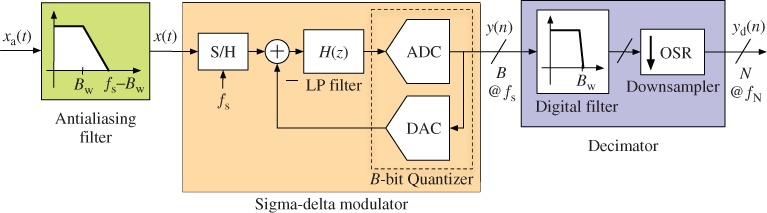
ADCs are electronic systems that perform the transformation of analog signals—which are continuous in time and in amplitude—into digital signals—which are discrete in both time and amplitude. Figure 1.1 illustrates the general block diagram of an ADC intended for the conversion of LP signals, which essentially consists of an antialiasing filter (AAF), a sampler, and a quantizer. First, the analog input signal ![]() of the ADC passes through the AAF, an LP analog filter than prevents out-of-band components from folding over the signal bandwidth
of the ADC passes through the AAF, an LP analog filter than prevents out-of-band components from folding over the signal bandwidth ![]() during the subsequent sampling, what would corrupt the signal information. The resulting band-limited signal
during the subsequent sampling, what would corrupt the signal information. The resulting band-limited signal ![]() is sampled at a rate
is sampled at a rate ![]() by the S/H circuit, thus yielding a DT signal
by the S/H circuit, thus yielding a DT signal ![]() , where
, where ![]() . Finally, the values of
. Finally, the values of ![]() are quantized using
are quantized using ![]() bits, so that each continuous-valued input sample is mapped onto the closer discrete-valued level out of the
bits, so that each continuous-valued input sample is mapped onto the closer discrete-valued level out of the ![]() that cover the input range, yielding the converter digital output
that cover the input range, yielding the converter digital output ![]() .
.
Figure 1.1 General block diagram of an A/D converter. A Nyquist-rate ADC is assumed.

As shown in Figure 1.1, the fundamental processes involved in the A/D conversion are sampling and quantization, whose implications are discussed in the following text.
1.1.1 Sampling
The sampling process performs the continuous-to-discrete transformation of the input signal in time and imposes a limit on the bandwidth of the analog input signal. According to the Nyquist theorem, to prevent information loss, ![]() must be sampled at a minimum rate of
must be sampled at a minimum rate of ![]() , often referred to as the Nyquist frequency. On the basis of this criterion, ADCs in which analog input signal is sampled at the minimum rate (
, often referred to as the Nyquist frequency. On the basis of this criterion, ADCs in which analog input signal is sampled at the minimum rate (![]() ) are called Nyquist-rate ADCs. Conversely, ADCs in which
) are called Nyquist-rate ADCs. Conversely, ADCs in which ![]() are called oversampling ADCs. How much faster than required the input signal is sampled is expressed in terms of the oversampling ratio (OSR), defined as
are called oversampling ADCs. How much faster than required the input signal is sampled is expressed in terms of the oversampling ratio (OSR), defined as
1.1 ![]()
Whether oversampling is used or not in an ADC has a noticeable influence on the requirements of its AAF. As in Nyquist-rate ADCs the input signal bandwidth ![]() coincides with
coincides with ![]() , aliasing will occur if
, aliasing will occur if ![]() in Figure 1.1 contains frequency components above
in Figure 1.1 contains frequency components above ![]() . High-order analog AAFs are thus required to implement sharp transition bands capable of removing out-of-band components with no significant attenuation of the signal band, as illustrated in Figure 1.2a for the LP case. Conversely, as
. High-order analog AAFs are thus required to implement sharp transition bands capable of removing out-of-band components with no significant attenuation of the signal band, as illustrated in Figure 1.2a for the LP case. Conversely, as ![]() in oversampling ADCs, the replicas of the input signal spectrum that are created by the sampling process are farther apart than in Nyquist-rate ADCs. As illustrated in Figure 1.2b, frequency components of the input signal in the range
in oversampling ADCs, the replicas of the input signal spectrum that are created by the sampling process are farther apart than in Nyquist-rate ADCs. As illustrated in Figure 1.2b, frequency components of the input signal in the range ![]() do not alias within the signal band, so that the filter transition band can be smoother, what greatly reduces the order required for the AAF and simplifies its design.
do not alias within the signal band, so that the filter transition band can be smoother, what greatly reduces the order required for the AAF and simplifies its design.
Figure 1.2 Antialiasing filter for (a) Nyquist-rate ADCs and (b) oversampling ADCs.

1.1.2 Quantization
The quantization process also introduces a limitation on the performance of an ideal ADC, because an error is generated while performing the continuous-to-discrete transformation of the input signal in amplitude, commonly referred to as quantization error. The operation of quantizers is illustrated in Figure 1.3. As a matter of example, Figure 1.3c depicts the I/O characteristic of a quantizer with ![]() , although results apply to a generic
, although results apply to a generic ![]() -bit quantizer. Input amplitudes within the full-scale input range
-bit quantizer. Input amplitudes within the full-scale input range ![]() are rounded to 1 out of the
are rounded to 1 out of the ![]() different output levels, which are usually encoded into a binary digital representation. If these levels are equally spaced, the quantizer is said to be uniform and the separation between adjacent output levels is defined as the quantization step
different output levels, which are usually encoded into a binary digital representation. If these levels are equally spaced, the quantizer is said to be uniform and the separation between adjacent output levels is defined as the quantization step
where ![]() stands for the full-scale output range. As
stands for the full-scale output range. As ![]() and
and ![]() are not necessarily equal, the quantizer may exhibit a gain different from unity, as indicated in Figure 1.3c by the slope
are not necessarily equal, the quantizer may exhibit a gain different from unity, as indicated in Figure 1.3c by the slope ![]() . As shown in Figure 1.3e, the quantizer operation thus inherently generates a rounding error that is a nonlinear function of the input. Note that, if
. As shown in Figure 1.3e, the quantizer operation thus inherently generates a rounding error that is a nonlinear function of the input. Note that, if ![]() is kept within the range
is kept within the range ![]() , the quantization error
, the quantization error ![]() is bounded within
is bounded within ![]() . The former input range is known as the nonoverload region of the quantizer, as opposed to ranges with
. The former input range is known as the nonoverload region of the quantizer, as opposed to ranges with ![]() , for which the magnitude of
, for which the magnitude of ![]() grows monotonously.
grows monotonously.
Figure 1.3 Illustration of the quantization process: (a) multibit quantizer block, (b) single-bit quantizer block, (c) I/O characteristic of a multibit quantizer, (d) I/O characteristic of a single-bit quantizer, (e) multibit quantization error, and (f) single-bit quantization error.
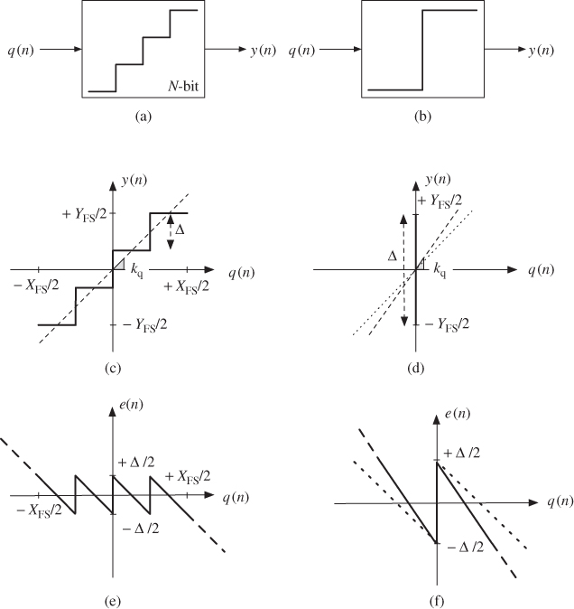
Figure 1.3 also shows the operation of a single-bit quantizer (![]() ). Note from Figure 1.3d that, compared to the multibit case, the output of a single-bit quantizer is determined by the input sign only, regardless of its magnitude. Therefore, the gain
). Note from Figure 1.3d that, compared to the multibit case, the output of a single-bit quantizer is determined by the input sign only, regardless of its magnitude. Therefore, the gain ![]() is undefined and can be arbitrarily chosen.
is undefined and can be arbitrarily chosen.
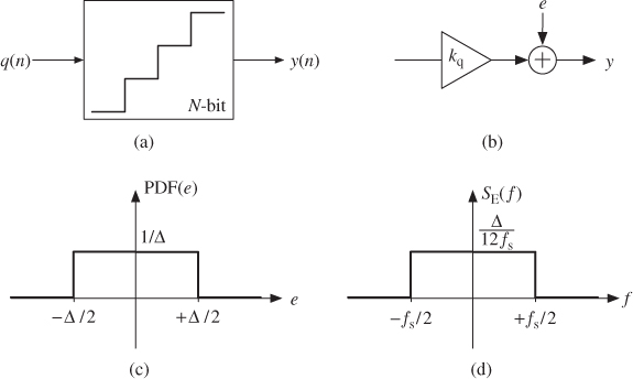
1.1.3 Quantization White Noise Model
In practice, an ideal quantizer as that shown in Figure 1.4a is often modeled using the linear scheme in Figure 1.4b if several assumptions are made on the statistical properties of the quantization error [1–3]. As already shown in Figure 1.3e, the quantization error ![]() is systematically determined by the quantizer input signal
is systematically determined by the quantizer input signal ![]() . Nevertheless, if
. Nevertheless, if ![]() is assumed to change randomly from sample to sample within the range
is assumed to change randomly from sample to sample within the range ![]() ,
, ![]() will also be uncorrelated from sample to sample. Under these requirements, the quantization error can be viewed as a random process with a uniform probability distribution in the range
will also be uncorrelated from sample to sample. Under these requirements, the quantization error can be viewed as a random process with a uniform probability distribution in the range ![]() , as illustrated in Figure 1.4c. The power associated to the quantization error can thus be computed as
, as illustrated in Figure 1.4c. The power associated to the quantization error can thus be computed as
1.3 
The former assumption implies that, as illustrated in Figure 1.4d, the power of the quantization error will also be uniformly distributed in the range ![]() , yielding
, yielding
1.4 
so that the power spectral density (PSD) of the quantization error in that range is
1.5 ![]()
These assumptions are collectively known as the additive white noise approximation
of the quantization error and allow the representation of a quantizer, which is deterministic and nonlinear, with the random linear model in Figure 1.4b, in which ![]() with
with ![]() being a quantization noise.1
being a quantization noise.1
Figure 1.4 Quantization noise: (a) multibit quantizer block, (b) equivalent linear model with additive white noise, (c) probability density function (PDF), and (d) power spectral density.
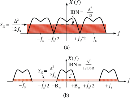
On the basis of this approximation of the quantization error to a white noise, the performance of ideal ADCs can be easily evaluated. For a Nyquist ADC, in which ![]() , all the quantization noise power falls inside the signal band and passes to the ADC output as a part of the input signal itself, as illustrated in Figure 1.5a. Conversely, if an oversampled signal is quantized, because
, all the quantization noise power falls inside the signal band and passes to the ADC output as a part of the input signal itself, as illustrated in Figure 1.5a. Conversely, if an oversampled signal is quantized, because ![]() , only a fraction of the total quantization noise power lies within the signal band, as illustrated in Figure 1.5b. The in-band noise power (IBN) caused by the quantization process in an ideal oversampling ADC is thus,
, only a fraction of the total quantization noise power lies within the signal band, as illustrated in Figure 1.5b. The in-band noise power (IBN) caused by the quantization process in an ideal oversampling ADC is thus,

so that the larger the OSR, the smaller the IBN.2
Figure 1.5 Quantization noise in (a) Nyquist-rate ADCs and (b) oversampling ADCs.
The dynamic range (DR) of an ideal ADC can be determined as the ratio of the output power at the frequency of an input sinusoid with maximum amplitude to the in-band quantization noise power:
1.7 ![]()
From Figure 1.3c, the maximum input amplitude in the nonoverload region of an ![]() -bit quantizer is
-bit quantizer is ![]() and its corresponding output power can be approximated to [5],
and its corresponding output power can be approximated to [5],
so that, using Equations 1.6 and 1.8, the DR of an ideal oversampling ADC yields
Note that, for a Nyquist ADC—that is, ![]() in Equation 1.9—each additional bit in the quantizer results in a DR increase of approximately
in Equation 1.9—each additional bit in the quantizer results in a DR increase of approximately ![]() . For an oversampling ADC, the DR further increases with the OSR by approximately
. For an oversampling ADC, the DR further increases with the OSR by approximately ![]() , so that using for instance an OSR of 4 is similar to having one extra bit in the
, so that using for instance an OSR of 4 is similar to having one extra bit in the ![]() -bit quantizer.
-bit quantizer.
1.1.4 Noise Shaping
An approach to further increase the accuracy of an oversampling ADC is shaping the quantization white noise in the frequency domain—that is, filtering it—in such a way that most of its power lies outside the signal band. This is illustrated in Figure 1.6a, where the quantization noise is conceptually obtained by subtracting the quantizer input signal ![]() from its output
from its output ![]() and then passes through a filter transfer function, usually called noise transfer function (NTF).
and then passes through a filter transfer function, usually called noise transfer function (NTF).
Figure 1.6 Quantization noise shaping: (a) conceptual block diagram and (b) effect on the in-band noise of an oversampling noise-shaping ADC.

For quantizers working on LP signals, the NTF is of high-pass type and can be easily obtained from a differentiator filter, with a ![]() -domain transfer function given by
-domain transfer function given by
where ![]() stands for the filter order. Taking into account that
stands for the filter order. Taking into account that ![]() , the magnitude of the pure-differentiator NTF in Equation 1.10 can be approximated for low frequencies to
, the magnitude of the pure-differentiator NTF in Equation 1.10 can be approximated for low frequencies to
so that the power due to the shaped quantization noise that lies within the signal band (Figure 1.6b) yields

Using Equations 1.8 and 1.12, the DR of an ideal oversampling noise-shaping ADC can be obtained as
Note that, in comparison with Equation 1.9, if oversampling is used in combination with noise shaping, the DR increases with OSR by approximately ![]() .
.
1.2 Basics of Sigma-Delta Modulators
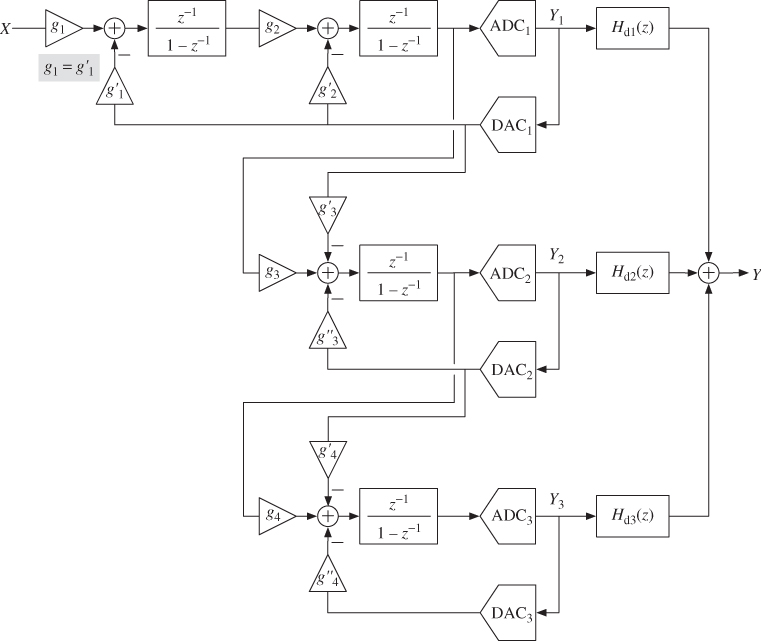
Contrary to the ADCs discussed so far, which are open loop systems from a control perspective, Sigma-Delta (![]() ) ADCs rely on a feedback path to achieve a closed-loop control of the quantization error. The fundamentals on how the shaping of quantization noise is implemented in practice, as well as the basic architecture, performance metrics, and ideal behavior of oversampling noise-shaping ADCs is presented in the following sections.
) ADCs rely on a feedback path to achieve a closed-loop control of the quantization error. The fundamentals on how the shaping of quantization noise is implemented in practice, as well as the basic architecture, performance metrics, and ideal behavior of oversampling noise-shaping ADCs is presented in the following sections.
1.2.1 Topology of  ADCs
ADCs
Figure 1.7 illustrates the basic block diagram of a ![]() ADC intended for the conversion of LP signals, which consists of the following:
ADC intended for the conversion of LP signals, which consists of the following:
- Antialiasing filter (AAF), which band limits the analog input signal to avoid aliasing during its subsequent sampling. As discussed in Section 1.1.1, oversampling considerably relaxes the attenuation requirements of the AAF, so that smooth transition bands are usually sufficient compared to Nyquist-rate ADCs.
- Sigma-Delta modulator (
 M), in which the oversampling and quantization of the band-limited analog signal take place. The quantization noise of the embedded
  -bit quantizer is shaped in the frequency domain by placing an appropriate loop filter
  before it and closing a negative feedback loop around them. Low-resolution quantizers, with
  typically in the range 1–5 bit, are sufficient for obtaining small IBN and high accuracy in the A/D conversion.
 - Decimation filter, in which a high-selectivity digital filter sharply removes the out-of-band spectral content of the
 M output and thus most of the shaped quantization noise. The decimator also reduces the data rate from
  down to the Nyquist frequency, while increasing the word length from
  to
to  bits to preserve resolution.
Figure 1.7 General block diagram of a ![]() ADC. A low-pass discrete-time
ADC. A low-pass discrete-time ![]() M is assumed.
M is assumed.
The ![]() modulator is the block that has most influence on the performance of the ADC, basically because it is responsible for the sampling and quantization processes that ultimately limit the accuracy of the A/D conversion. We will focus on this block from now on, although it must be kept in mind that a
modulator is the block that has most influence on the performance of the ADC, basically because it is responsible for the sampling and quantization processes that ultimately limit the accuracy of the A/D conversion. We will focus on this block from now on, although it must be kept in mind that a ![]() ADC is more than a
ADC is more than a ![]() M!
M!
1.2.2 Signal Processing in  Ms
Ms
The basic scheme of a ![]() modulator consists of a loop filter
modulator consists of a loop filter ![]() and a
and a ![]() -bit quantizer in a feedback loop, as shown in Figure 1.8a [6]. Let us consider that the gain of the loop filter is large within the signal band and small outside it. Owing to the action of negative feedback, the analog input signal
-bit quantizer in a feedback loop, as shown in Figure 1.8a [6]. Let us consider that the gain of the loop filter is large within the signal band and small outside it. Owing to the action of negative feedback, the analog input signal ![]() and the analog version of the
and the analog version of the ![]() M output
M output ![]() will practically coincide within the signal band, so that the error signal
will practically coincide within the signal band, so that the error signal ![]() in this closed-loop system is very small within the signal band. As the
in this closed-loop system is very small within the signal band. As the ![]() -bit quantizer is uniform, mostof the differences between the input and the output of the
-bit quantizer is uniform, mostof the differences between the input and the output of the ![]() M will be placed at higher frequencies, so that the quantization noise is shaped in the frequency domain and most of its power is pushed outside the signal band.
M will be placed at higher frequencies, so that the quantization noise is shaped in the frequency domain and most of its power is pushed outside the signal band.
Figure 1.8 ![]() modulator: (a) block diagram and (b) ideal linear model.
modulator: (a) block diagram and (b) ideal linear model.
Using the linear additive white noise model in Figure 1.4b for the embedded quantizer, the ![]() M in Figure 1.8a can be modeled as the two-input (
M in Figure 1.8a can be modeled as the two-input (![]() and
and ![]() ) one-output (
) one-output (![]() ) linear system in Figure 1.8b, which is described in the
) linear system in Figure 1.8b, which is described in the ![]() -domain as
-domain as
1.14 ![]()
where STF and NTF stand for the signal and noise transfer functions, respectively given by
1.15 ![]()
Note that, if the loop filter is designed such that ![]() within the signal band, then
within the signal band, then ![]() and
and ![]() ; that is, the quantization noise is ideally canceled while the input signal is perfectly transferred to the output.
; that is, the quantization noise is ideally canceled while the input signal is perfectly transferred to the output.
For the conversion of LP signals, the simplest loop filter ![]() that exhibits the desired frequency performance is an integrator,
that exhibits the desired frequency performance is an integrator,
that, in combination with an embedded quantizer with ![]() , leads to a
, leads to a ![]() M whose output is given by
M whose output is given by
1.17 ![]()
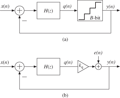
and builds up a first-order, high-pass shaping of the quantization noise—see Equation 1.10. For the sake of illustration, Figure 1.9 shows the output signal of a first-order ![]() M with a embedded 3-bit (8-level) quantizer for a sinusoidal input signal. Note that, due to the combined action of oversampling and negative feedback, the modulator output is a pulse-density modulated (PDM) signal whose local average tracks the input signal value within adjacent code transitions.
M with a embedded 3-bit (8-level) quantizer for a sinusoidal input signal. Note that, due to the combined action of oversampling and negative feedback, the modulator output is a pulse-density modulated (PDM) signal whose local average tracks the input signal value within adjacent code transitions.
Figure 1.9 PDM output signal of a first-order, ![]() modulator with an embedded 3-bit quantizer for an input sinusoid.
modulator with an embedded 3-bit quantizer for an input sinusoid.
1.2.3 Performance Metrics of  Ms
Ms
Contrary to Nyquist-rate ADCs, whose performance is mainly characterized by static performance metrics—that is, monotonicity, gain and offset errors, differential nonlinearity (DNL), and integral nonlinearity (INL) [5]—![]() ADCs' characteristics are typically measured using dynamic performance metrics, which are obtained from the frequency-domain representation of the time-domain digital output sequence. The latter thus requires the computation of the fast Fourier transform (FFT) of a finite-length output sequence with a specific windowing function, as will be discussed in Chapter 4. From that power spectrum representation of a
ADCs' characteristics are typically measured using dynamic performance metrics, which are obtained from the frequency-domain representation of the time-domain digital output sequence. The latter thus requires the computation of the fast Fourier transform (FFT) of a finite-length output sequence with a specific windowing function, as will be discussed in Chapter 4. From that power spectrum representation of a ![]() M output sequence, some spectral metrics are directly measured and other noise and power metrics are derived.
M output sequence, some spectral metrics are directly measured and other noise and power metrics are derived.
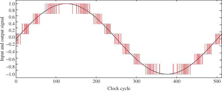
Figure 1.10 illustrates an exemplary spectrum of a ![]() M output sequence when a sinusoidal signal with frequency
M output sequence when a sinusoidal signal with frequency ![]() is applied at its input. The main characteristics of the spectrum are highlighted; for example, the length of the digital sequence from which the FFT has been computed, the output signal peak at the frequency
is applied at its input. The main characteristics of the spectrum are highlighted; for example, the length of the digital sequence from which the FFT has been computed, the output signal peak at the frequency ![]() corresponding to the converted signal, etc. As will be discussed in Chapter 2, nonidealities of the circuitry used for implementing the
corresponding to the converted signal, etc. As will be discussed in Chapter 2, nonidealities of the circuitry used for implementing the ![]() M deviate in practice the output spectrum from a purely shaped quantization noise. On the one hand, linear errors give rise to a noise floor, as well as to a degradation of the shaping order. On the other, nonlinear errors generate distortion, which is typically noticeable for large input amplitudes, but submerged under the noise floor for small input signal amplitudes. Spectral metrics such as the spurious-free dynamic range (SFDR)—that is, the ratio of the signal power to the strongest spectral tone [5]—can be directly measured from the output modulator spectrum, as shown in Figure 1.10.
M deviate in practice the output spectrum from a purely shaped quantization noise. On the one hand, linear errors give rise to a noise floor, as well as to a degradation of the shaping order. On the other, nonlinear errors generate distortion, which is typically noticeable for large input amplitudes, but submerged under the noise floor for small input signal amplitudes. Spectral metrics such as the spurious-free dynamic range (SFDR)—that is, the ratio of the signal power to the strongest spectral tone [5]—can be directly measured from the output modulator spectrum, as shown in Figure 1.10.
Figure 1.10 Illustration of a typical output spectrum of a ![]() modulator and its main characteristics. A low-pass
modulator and its main characteristics. A low-pass ![]() M is assumed.
M is assumed.
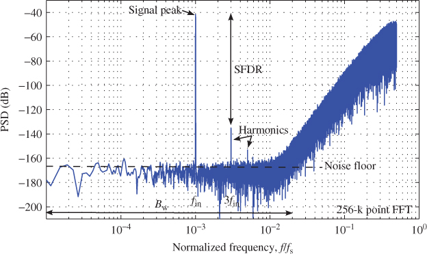
Noise and power metrics are derived from the ![]() M output spectra by integration over the signal bandwidth and are typically collected in a single plot as shown in Figure 1.11. These metrics are usually the most important measures and comprise the following:
M output spectra by integration over the signal bandwidth and are typically collected in a single plot as shown in Figure 1.11. These metrics are usually the most important measures and comprise the following:
- Signal-to-noise ratio (SNR), which is the ratio of the output power at the frequency of an input sinusoid to the uncorrelated IBN:
1.18

It accounts for the modulator linear performance only, so that the in-band power associated to harmonics of the input signal is not considered as part of the IBN for SNR computation.If an ideal
 M is considered and only the in-band quantization noise is accounted for in the IBN computation, the term signal-to-quantization-noise ratio (SQNR) is often employed.
 - Signal-to-noise-plus-distortion ratio (SNDR), which is defined as the ratio of the output power at the frequency of an input sinusoid to the total IBN power, also accounting for possible harmonics at the
 M output. As illustrated in Figure 1.11, this makes a typical SNDR curve to deviate from the SNR curve only for large input amplitudes, for which the generated distortion is noticeable. Therefore, the output spectra from which the SNDR curve is computed are typically obtained by applying an input signal at
  (for LP
  Ms), so that at least the second and third harmonics lie within the signal band.
 - Dynamic range (DR), which can be defined as the ratio of the output power at the frequency of an input sinusoid with maximum amplitude to the output power for a small input amplitude for which
 ; that is, so it cannot be distinguished from the error. Ideally, a sinusoid with maximum amplitude at the modulator input will provide an output sinusoid sweeping the full-scale range
  of the embedded quantizer, so that
- Effective number of bits (ENOB): as the DR of an ideal
 -bit Nyquist-rate converter is given by Equation 1.9 with
  , a similar expression can be established for
  Ms
Ms
where ENOB can be defined as the number of bits needed for an ideal Nyquist-rate ADC to achieve the same DR as the
 ADC. The performance of oversampled
  converters and Nyquist-rate ADCs can thus be compared in a simple way [7].Instead of the DR, the peak SNDR is also often used in Equation 1.20 to express the accuracy of the A/D in a
  modulator in bits.
 - Overload Level (OL): as illustrated in Figure 1.11, the SNR of a
 modulator increases monotonously with the input signal amplitude (
 ), but sharply drops for input amplitudes close to half of the full-scale input range of the embedded quantizer (
 ) due to its overload and the associated IBN increase. The overload level is considered to define the maximum input amplitude for which the
  M still operates correctly and can almost be arbitrarily defined, but it is typically chosen as the amplitude for which the SNR drops
  below the peak SNR [8].
Figure 1.11 Illustration of the performance metrics of a ![]() modulator on a typical SNR curve.
modulator on a typical SNR curve.
1.2.4 Performance Enhancement of  Ms
Ms
The output of an ideal LP ![]() th-order
th-order ![]() modulator in the
modulator in the ![]() -domain can be considered to be
-domain can be considered to be
where ![]() and the NTF builds up an
and the NTF builds up an ![]() th-order high-pass shaping of the quantization noise of the embedded quantizer. If a
th-order high-pass shaping of the quantization noise of the embedded quantizer. If a ![]() -bit quantizer is employed, the DR of the
-bit quantizer is employed, the DR of the ![]() M can be obtained from Equations 1.12 and 1.19 to ideally yield
M can be obtained from Equations 1.12 and 1.19 to ideally yield

taking into account that ![]() —see Equation 1.2 —and considering quantization noise as the only contribution to the IBN.
—see Equation 1.2 —and considering quantization noise as the only contribution to the IBN.
Note from Equation 1.22 that the DR of a ![]() modulator is ideally determined by the values of
modulator is ideally determined by the values of ![]() , OSR, and
, OSR, and ![]() , which can thus be considered as the three key parameters that define the
, which can thus be considered as the three key parameters that define the ![]() M at the high level. The pros and cons of increasing the DR of a
M at the high level. The pros and cons of increasing the DR of a ![]() modulator by increasing each of these parameters are briefly discussed in the following:
modulator by increasing each of these parameters are briefly discussed in the following:
- High-order
 modulators. The accuracy of the A/D conversion can be considerably improved by increasing the noise-shaping order, because a larger fraction of the total quantization noise power will be pushed out of the signal band. Figure 1.12 illustrates the ideal noise-shaping functions of orders ranging from 1 to 5. The case
  —that is, no shaping—is also included for comparison purposes. The DR enhancement if
  is increased in one for a given OSR can be obtained from Equation 1.22 to be
1.23

This means that, for instance, the DR of a fourth-order
 M with
  is ideally
  (
( ) larger than that of a third-order
  M. However, as will be discussed in Section 1.4.2, the use of high-order (
 ) loop filters gives rise to stability problems in a
  M. Although these problems can be circumvented, the DR of a high-order
  M will in practice be smaller than predicted in Equation 1.22.
 - High OSR
 modulators. Figure 1.13 shows the ideal DR as a function of OSR for noise-shaping orders ranging from 0 (no shaping) to 5 and assuming a single-bit embedded quantizer (
 ). As illustrated, the combination of oversampling and noise-shaping considerably enhances the
  M performance for
  . Note from Equation 1.22 that the DR of an ideal
  th-order
  modulator increases with OSR in
 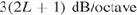 . However, for a given conversion bandwidth
  , the OSR cannot be arbitrarily increased, because it leads to a higher sampling frequency
  for the operation of the
  circuitry. The latter, if achievable in practice for a given technological process, leads to larger power consumption.
 - Multibit
 modulators. An increase in
  leads to a decrease of the quantization step
  and thus to a reduction of the quantization noise power. Each additional bit in the embedded quantizer of a
  M is considered to typically yield a 6 dB (1 bit) improvement on the DR [9]. However, a multibit embedded quantizer requires a multilevel DAC to close the negative feedback loop in the
  M. Contrary to a two-level feedback DAC (
 ), which is inherently linear, a multilevel DAC will in practice be nonlinear to some extent. As noticeable from Figure 1.14, the DAC nonlinearity will be directly added to the
  M input and will thus appear at the output, as
  within the signal band. Therefore, the linearity required in a multibit DAC equals in practice that wanted for the
  modulator. This point will be further discussed in Section 1.6.
Figure 1.12 Illustration of the shaping of quantization noise as a function of frequency in a ![]() M. NTF is given by Equation 1.10 and
M. NTF is given by Equation 1.10 and ![]() stands for the noise-shaping order.
stands for the noise-shaping order.
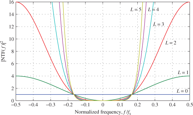
Figure 1.13 Ideal dynamic range of a ![]() M as a function of the oversampling ratio for different noise-shaping orders (
M as a function of the oversampling ratio for different noise-shaping orders (![]() ). A single-bit internal quantizer (
). A single-bit internal quantizer (![]() ) is assumed.
) is assumed.

Figure 1.14 Second-order ![]() modulator with unity STF.
modulator with unity STF.

1.3 Classification of  Modulators
The strategies discussed in Section 1.2.4 for improving the DR of a ![]() M may be combined in many different ways, giving rise to the huge number of
M may be combined in many different ways, giving rise to the huge number of ![]() M topologies reported in literature, which can be grouped attending to different classification criteria [10]:
M topologies reported in literature, which can be grouped attending to different classification criteria [10]:
- Single-Loop versus Cascade
 Ms (attending to the number of quantizers employed).
  Ms employing only one quantizer are called single-loop
topologies, whereas those employing several quantizers are often named cascade or MASH
Ms employing only one quantizer are called single-loop
topologies, whereas those employing several quantizers are often named cascade or MASH  Ms. These topological alternatives will be discussed in Sections 1.4 and 1.5.
 - Single-Bit versus Multibit
 Ms (attending to the number of bits in the embedded quantizer). Their pros and cons will be discussed in Section 1.6.
 - Low-Pass versus Band-Pass
 Ms (attending to the nature of the signals being converted). The A/D conversion of LP signals has been assumed in previous sections, but BP
  Ms can also be built, as will be discussed in Section 1.7.
 - Discrete-Time versus Continuous-Time
 Ms (attending to the nature of loop filter dynamics). The use of a DT loop filter in the
  M has been assumed in previous sections. However, CT
  Ms can be also implemented in practice. According to this classification criteria, hybrid CT/DT
  Ms take advantage of the benefits of both DT and CT implementations, which will be discussed in Section 1.8.
Describing all possible ![]() M architectures derived from previous classification criteria goes beyond the scope of this book. A detailed analysis of them can be found in the many papers and books devoted to the topic in the
M architectures derived from previous classification criteria goes beyond the scope of this book. A detailed analysis of them can be found in the many papers and books devoted to the topic in the ![]() literature [4, 9, 11–23]. Instead, we will hereafter focus on the most representative families of
literature [4, 9, 11–23]. Instead, we will hereafter focus on the most representative families of ![]() modulators.
modulators.
1.4 Single-Loop  Modulators
![]() modulators that make use of only one embedded quantizer are usually referred to as single-loop topologies. To get familiar with these architectures, their performance, their circuit-level implementation, as well as some other practical aspects are first addressed considering the case of second-order
modulators that make use of only one embedded quantizer are usually referred to as single-loop topologies. To get familiar with these architectures, their performance, their circuit-level implementation, as well as some other practical aspects are first addressed considering the case of second-order ![]() Ms. Afterward, the problematics of stability in higher-order
Ms. Afterward, the problematics of stability in higher-order ![]() Ms is presented, together with architectural alternatives to circumvent it.
Ms is presented, together with architectural alternatives to circumvent it.
1.4.1 Second-Order  M
M
Figure 1.15a shows a second-order ![]() modulator built up by cascading two DT integrators [24], with each integrator receiving a weighted feedback path from the DAC. Coefficients
modulator built up by cascading two DT integrators [24], with each integrator receiving a weighted feedback path from the DAC. Coefficients ![]() are usually called integrator scalings or weights. Under linear analysis, the modulator output in the
are usually called integrator scalings or weights. Under linear analysis, the modulator output in the ![]() -domain yields
-domain yields

where ![]() stands for the gain of the quantizer. For a pure second-order shaping, Equation 1.24 needs to be simplified to
stands for the gain of the quantizer. For a pure second-order shaping, Equation 1.24 needs to be simplified to
1.25 ![]()
so that the following expressions for the integrator coefficients need to be fulfilled:
Figure 1.15 Block diagram of second-order ![]() Ms and different notations: (a) general representation of the DT-
Ms and different notations: (a) general representation of the DT-![]() M using the notation in [8, 9] and (b) alternative representation of the DT-
M using the notation in [8, 9] and (b) alternative representation of the DT-![]() M using the notation in [12, 19].
M using the notation in [12, 19].

Figure 1.15b shows an alternative representation of the second-order ![]() M according to the coefficients notation in [12, 19], which allows to allocate different weights in the forward and feedback paths of each integrator, using coefficients
M according to the coefficients notation in [12, 19], which allows to allocate different weights in the forward and feedback paths of each integrator, using coefficients ![]() and
and ![]() , respectively. As exemplary illustrated in Figure 1.16, the notations in Figure 1.15a and b can be easily connected with the equalities:
, respectively. As exemplary illustrated in Figure 1.16, the notations in Figure 1.15a and b can be easily connected with the equalities:

Figure 1.16 Illustration of the equivalence between the DT representations in Figure 1.15a and 1.14b.

Both nomenclatures for the integrator scaling coefficients of ![]() modulators will be used throughout this book. The notation in [8, 9] is closer to the modulator architectural level, whereas the notation in [12, 19] is closer to the actual circuit-level implementation, in which integrators with more than one SC input branch are usually employed. The latter is thus useful to accurately account for some nonidealities of the practical
modulators will be used throughout this book. The notation in [8, 9] is closer to the modulator architectural level, whereas the notation in [12, 19] is closer to the actual circuit-level implementation, in which integrators with more than one SC input branch are usually employed. The latter is thus useful to accurately account for some nonidealities of the practical ![]() M implementation, which will be covered in Chapter 2.
M implementation, which will be covered in Chapter 2.
For the sake of illustration, Figure 1.17 shows a possible implementation of the second-order ![]() M in Figure 1.15 using fully-differential SC circuitry and assuming single-bit quantization. The modulator differential input signal is denoted by
M in Figure 1.15 using fully-differential SC circuitry and assuming single-bit quantization. The modulator differential input signal is denoted by ![]() and the modulator digital output
and the modulator digital output ![]() , after the comparator, controls the feedback connection of reference voltages
, after the comparator, controls the feedback connection of reference voltages ![]() and
and ![]() to the integrators. The modulator full scale range
to the integrators. The modulator full scale range ![]() thus equals
thus equals ![]() , with
, with ![]() . Note from the first SC integrator in Figure 1.17 that both the modulator input signal and the DAC feedback signal are processed through the sampling capacitor
. Note from the first SC integrator in Figure 1.17 that both the modulator input signal and the DAC feedback signal are processed through the sampling capacitor ![]() . For the second integrator, the output of the first integrator is processed through both
. For the second integrator, the output of the first integrator is processed through both ![]() and
and ![]() , whereas the DAC feedback signal is processed only through
, whereas the DAC feedback signal is processed only through ![]() . The modulator scaling coefficients are thus implemented as the following capacitor ratios (Figure 1.15b)
. The modulator scaling coefficients are thus implemented as the following capacitor ratios (Figure 1.15b)
1.28 
Figure 1.17 Fully-differential SC implementation of a second-order ![]() modulator.
modulator.

In practice, the value of the integrator weights are selected to fulfill the relations in Equation 1.26, also taking into account their implication in some aspects of the modulator performance, such as the following:
- Keeping the state variables (integrator outputs) bounded to ensure the modulator stability. The second-order
 M is stable for inputs in the range
  if
if  , regardless the quantizer gains
  [24]. This condition is already met if
  —see Equations 1.26 and 1.27.
 - Keeping the modulator overload level as close as possible to the full scale to ensure a high-peak SNR—see Figure 1.11.
- Minimizing the required signal range at the integrators outputs; that is, the integrator output swing demands must be attainable with the intended voltage supply and as low as possible to reduce power consumption and to facilitate circuit design.
- Simplifying the practical implementation of the integrator weights as ratios of unit capacitors.
Generally speaking, the selection of the scaling coefficients of a ![]() modulator involves solving several trade-offs between architectural-, circuit-, and technological-level aspects of the practical implementation, so that the optimum selection for a given application may not apply in a different scenario. For the sake of illustration, Table 1.1 shows several sets of weights reported for the second-order, single-bit
modulator involves solving several trade-offs between architectural-, circuit-, and technological-level aspects of the practical implementation, so that the optimum selection for a given application may not apply in a different scenario. For the sake of illustration, Table 1.1 shows several sets of weights reported for the second-order, single-bit ![]() M in Figure 1.15. All sets exhibit an overload level
M in Figure 1.15. All sets exhibit an overload level ![]() (i.e.,
(i.e., ![]() below the full-scale amplitude
below the full-scale amplitude ![]() ). The required integrator output swing and the minimum number of unit capacitors are also included. Capacitor sharing between weights in the same integrator has been considered.
). The required integrator output swing and the minimum number of unit capacitors are also included. Capacitor sharing between weights in the same integrator has been considered.
Table 1.1 Comparison of some sets of coefficients reported for the second-order single-bit ![]() M
M

Second-Order  M with Unity STF
Figure 1.14 shows an alternative second-order ![]() M topology that makes use of feed-forward paths to implement a so-called unity STF [28, 29]. Under linear analysis, the modulator output in the
M topology that makes use of feed-forward paths to implement a so-called unity STF [28, 29]. Under linear analysis, the modulator output in the ![]() -domain yields
-domain yields
1.29 ![]()
so that ![]() —that is, the signal transfer function equals 1 at all frequencies—whereas NTF is unaffected.
—that is, the signal transfer function equals 1 at all frequencies—whereas NTF is unaffected.
One of the most appealing features of the unity-STF ![]() M in Figure 1.14 is that ideally there is no input signal trace processed by the integrators. Indeed, the integrator inputs in
M in Figure 1.14 is that ideally there is no input signal trace processed by the integrators. Indeed, the integrator inputs in ![]() -domain can be obtained as
-domain can be obtained as
1.30 ![]()
showing that they depend only on the quantization error. In practice, there will be some residual component of the modulator input signal at the integrator inputs, but it is normally negligible. This means that, if nonlinearities of the circuit implementation are accounted for, the generated distortion will be considerably lower for the unity-STF ![]() M in Figure 1.14 compared to the one traditional
M in Figure 1.14 compared to the one traditional ![]() M in Figure 1.15. Moreover, the technique is effective for any OSR, which makes unity-STF
M in Figure 1.15. Moreover, the technique is effective for any OSR, which makes unity-STF ![]() Ms especially suited for lowering the sensitivity to circuit imperfections in wideband applications, in which low OSR values are required.
Ms especially suited for lowering the sensitivity to circuit imperfections in wideband applications, in which low OSR values are required.
The described concept of unity STF can be extended to a noise shaping of any order. The only requirement is to ideally make ![]() , without changing the modulator NTF. In recent years, it has been often applied in
, without changing the modulator NTF. In recent years, it has been often applied in ![]() Ms for wideband and multimode applications [30–34].
Ms for wideband and multimode applications [30–34].
1.4.2 High-Order  Ms
Ms
The simplest way to extend a ![]() M to an arbitrary
M to an arbitrary ![]() th-order shaping consists of including
th-order shaping consists of including ![]() integrators before the quantizer. Extending the second-order
integrators before the quantizer. Extending the second-order ![]() M in Figure 1.15a, the topology in Figure 1.18 is obtained, which is known as an
M in Figure 1.15a, the topology in Figure 1.18 is obtained, which is known as an ![]() th-order single-loop
th-order single-loop ![]() M with distributed feedback [35].3 Ideally, its NTF can be derived from linear analysis and equated to Equation 1.10 to derive a set of relations between the integrator scaling coefficients to be fulfilled for obtaining a pure-differentiator noise shaping—similarly as done in Equation 1.26 for the second-order
M with distributed feedback [35].3 Ideally, its NTF can be derived from linear analysis and equated to Equation 1.10 to derive a set of relations between the integrator scaling coefficients to be fulfilled for obtaining a pure-differentiator noise shaping—similarly as done in Equation 1.26 for the second-order ![]() M. The in-band quantization noise and the modulator DR would thus be ideally given by Equations 1.12 and 1.13, respectively.
M. The in-band quantization noise and the modulator DR would thus be ideally given by Equations 1.12 and 1.13, respectively.
Figure 1.18 High-order single-loop ![]() M with distributed feedback.
M with distributed feedback.
However, this modulator performance cannot be met in practice because ![]() Ms with pure-differentiator FIR NTFs are prone to instability if
Ms with pure-differentiator FIR NTFs are prone to instability if ![]() , exhibiting unbounded states and poor SNR compared to that predicted by linear analysis. In general, instability appears at the modulator output as a large-amplitude, low-frequency oscillation, leading to long bitstreams of alternating
, exhibiting unbounded states and poor SNR compared to that predicted by linear analysis. In general, instability appears at the modulator output as a large-amplitude, low-frequency oscillation, leading to long bitstreams of alternating ![]() s and
s and ![]() s. This tendency to instability can be explained as follows [36]. For a
s. This tendency to instability can be explained as follows [36]. For a ![]() M to be stable, the quantizer input must not be allowed to become too large. As the quantizer input is obtained as (Figure 1.18)
M to be stable, the quantizer input must not be allowed to become too large. As the quantizer input is obtained as (Figure 1.18)
1.31 ![]()
the gain of ![]() , or simply
, or simply ![]() , must not be too large. However, as clearly visible from Figure 1.12, the out-of-band gain of FIR NTFs of the form
, must not be too large. However, as clearly visible from Figure 1.12, the out-of-band gain of FIR NTFs of the form ![]() rapidly increases for
rapidly increases for ![]() , yielding
, yielding ![]() at
at ![]() . Consequently, it starts to overload the quantizer, which yields a significant decrease of the modulator SNR.
. Consequently, it starts to overload the quantizer, which yields a significant decrease of the modulator SNR.
This problem can be circumvented by resorting to single-loop ![]() Ms with IIR NTFs of the form
Ms with IIR NTFs of the form ![]() , with
, with ![]() being a polynomial determined by the modulator scaling coefficients that helps to limit the out-of-band gain of NTF.4 However, unlike second-order
being a polynomial determined by the modulator scaling coefficients that helps to limit the out-of-band gain of NTF.4 However, unlike second-order ![]() Ms, for which a stability condition has been extracted [24], determining exact conditions that guarantee the stability of higher-order, single-loop
Ms, for which a stability condition has been extracted [24], determining exact conditions that guarantee the stability of higher-order, single-loop ![]() Ms is still an open question. In [8, 37], it is shown, using behavioral simulations, that high-order
Ms is still an open question. In [8, 37], it is shown, using behavioral simulations, that high-order ![]() Ms are conditionally stable; that is, with proper selection of the scaling coefficients, a stable operation can be obtained for inputs restricted within a certain range and for certain initial conditions of the state variables. However, despite the absence of general stability conditions, high-order
Ms are conditionally stable; that is, with proper selection of the scaling coefficients, a stable operation can be obtained for inputs restricted within a certain range and for certain initial conditions of the state variables. However, despite the absence of general stability conditions, high-order ![]() Ms have been successfully designed since the late 1980s [38]. Indeed, the topology in Figure 1.18 has been widely used and optimal coefficients for it have been presented in [8].
Ms have been successfully designed since the late 1980s [38]. Indeed, the topology in Figure 1.18 has been widely used and optimal coefficients for it have been presented in [8].
Its STF and NTF can be calculated under linear analysis as5

because of its simplicity and its good agreement with simulation results.


If integrators described by Equation 1.16 are used as filters—![]() —the NTF can be approximated for low frequencies to [8]
—the NTF can be approximated for low frequencies to [8]
1.35 ![]()
in which the complete scaling of the outermost feedback branch of the ![]() M dominates the noise-shaping behavior. Similarly as done Equations 1.11 and 1.12, the IBN of an
M dominates the noise-shaping behavior. Similarly as done Equations 1.11 and 1.12, the IBN of an ![]() th-order, single-loop
th-order, single-loop ![]() M with distributed feedback thus yields
M with distributed feedback thus yields
so that the IBN increases by a factor ![]() compared to an ideal
compared to an ideal ![]() M.
M.
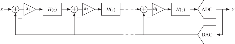
A major drawback of this loop filter implementation in Figure 1.18 is that the integrator outputs contain a significant amount of the input signal [41], so that the integrators require significant swing capabilities and/or the scaling coefficients need to be low. This can be circumvented using the loop filter topology in Figure 1.19, which is a chain of integrators with feed-forward summation [42]. Under linear analysis, the corresponding STF and NTF can be calculated as

Note that NTF structure is the same as in Equation 1.34; therefore, the IBN of this ![]() M topology yields an expression similar to that in Equation 1.36.
M topology yields an expression similar to that in Equation 1.36.
Figure 1.19 High-order single-loop ![]() M with feed-forward summation.
M with feed-forward summation.
However, for the case of the distributed feedback topology in Figure 1.18 and the feed-forward summation topology in Figure 1.19, the loop filter for the STF and the NTF are essentially identical—compare Equation 1.33 with 1.34 and Equation 1.37 with 1.38. This means that, if the NTF is designed for the desired noise-shaping behavior, both topologies also fix the STF function, as ![]() [41].6
[41].6
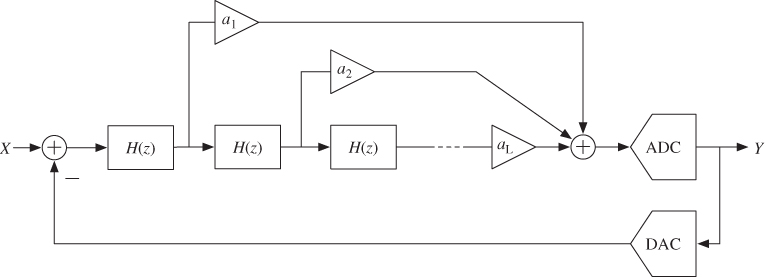
If a certain degree of freedom is desired in designing both the modulator NTF and STF, the topology in Figure 1.20 can be used, which is a chain of integrators with distributed feedback and distributed feed-forward input paths [43]. In this architecture, the zeros of STF can be fixed with coefficients ![]() without affecting the pole placement, so both STF and NTF can be separately optimized to some extent [41].7
without affecting the pole placement, so both STF and NTF can be separately optimized to some extent [41].7
Figure 1.20 High-order single-loop ![]() M with distributed feedback and distributed feed-forward input paths.
M with distributed feedback and distributed feed-forward input paths.

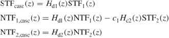
1.5 Cascade  Modulators
As discussed in Section 1.4.2, stability problems arising from implementing a high-order NTF with a single-loop ![]() M can be circumvented with adequate scaling coefficients, but they result in a significant decrease of the DR compared with an ideal
M can be circumvented with adequate scaling coefficients, but they result in a significant decrease of the DR compared with an ideal ![]() M. An alternative approach to obtain a high-order noise shaping while avoiding instabilities is found in the so-called cascade
M. An alternative approach to obtain a high-order noise shaping while avoiding instabilities is found in the so-called cascade ![]() Ms, also known as multiloop
Ms, also known as multiloop ![]() Ms or multistage noise shaping (MASH)
Ms or multistage noise shaping (MASH) ![]() Ms [45–48]. Their architecture is illustrated in Figure 1.21 and consists of
Ms [45–48]. Their architecture is illustrated in Figure 1.21 and consists of ![]() stages of
stages of ![]() modulators, in which each stage remodulates a scaled version of the quantization error generated in the preceding one. The outputs of the cascaded stages
modulators, in which each stage remodulates a scaled version of the quantization error generated in the preceding one. The outputs of the cascaded stages ![]() are conveniently processed in digital domain to cancel out at the overall
are conveniently processed in digital domain to cancel out at the overall ![]() M output
M output ![]() all the quantization errors, but that of the back-end stage. In addition, the latter quantization error appears at the cascade output shaped with an order
all the quantization errors, but that of the back-end stage. In addition, the latter quantization error appears at the cascade output shaped with an order ![]() equal to the summation of those of the cascaded stages (
equal to the summation of those of the cascaded stages (![]() ). Unconditionally, stable high-order shaping can thus be obtained if only first- and second-order
). Unconditionally, stable high-order shaping can thus be obtained if only first- and second-order ![]() Ms are cascaded (
Ms are cascaded (![]() ), because all feedback loops are local to the low-order
), because all feedback loops are local to the low-order ![]() stages and there is no interstage feedback. Therefore, the performance of a multistage
stages and there is no interstage feedback. Therefore, the performance of a multistage ![]() M is similar to that of an ideal high-order, single-loop with no stability issues.8
M is similar to that of an ideal high-order, single-loop with no stability issues.8
Figure 1.21 General topology of an ![]() -stage cascade
-stage cascade ![]() modulator.
modulator.

The operation principle of cascade ![]() Ms can be easily understood considering an exemplary two-stage cascade. Using linear analysis, the stages output can be expressed in the
Ms can be easily understood considering an exemplary two-stage cascade. Using linear analysis, the stages output can be expressed in the ![]() -domain as
-domain as
1.39 ![]()
where the input of the ![]() stages are given by
stages are given by ![]() and
and ![]() , and
, and ![]() and
and ![]() stand for the quantization error of the respective stage. The overall modulator output after the digital cancelation logic (DCL) can thus be obtained from the expressions above as
stand for the quantization error of the respective stage. The overall modulator output after the digital cancelation logic (DCL) can thus be obtained from the expressions above as
1.40 ![]()
where ![]() ,
, ![]() , and
, and ![]() stand for the overall cascade transfer functions for the input signal and the quantization errors, respectively
stand for the overall cascade transfer functions for the input signal and the quantization errors, respectively
Note that, if the signal processing in the DCL matches part of the signal processing in the analog side, Equation 1.41 yields
1.42 
so that the first-stage quantization error is canceled at the overall output and that of the second stage is attenuated with an order equal to the summation of both stages' orders (![]() ).
).
For the generic ![]() -stage cascade
-stage cascade ![]() M in Figure 1.21, assuming
M in Figure 1.21, assuming ![]() and
and ![]() in the individual stages, the overall modulator output thus yields
in the individual stages, the overall modulator output thus yields
under the required matching between the analog processing in the ![]() stages and the DCL. The in-band quantization noise of the cascade is then given by
stages and the DCL. The in-band quantization noise of the cascade is then given by
where ![]() stands for the quantization step employed in the last
stands for the quantization step employed in the last ![]() stage. Note from Equation 1.44 that only the interstage scaling coefficients
stage. Note from Equation 1.44 that only the interstage scaling coefficients ![]() , which prevent a premature overload of the subsequent stages, decrease the performance below that of an ideal
, which prevent a premature overload of the subsequent stages, decrease the performance below that of an ideal ![]() th order
th order ![]() M. Typical values of
M. Typical values of ![]() are between 2 and 4 if single-bit quantization is employed, which lead to a reduction in the ideally attainable DR of only 6–12 dB (1–2 bit). These performance losses are inherent to cascade
are between 2 and 4 if single-bit quantization is employed, which lead to a reduction in the ideally attainable DR of only 6–12 dB (1–2 bit). These performance losses are inherent to cascade ![]() Ms, but they are significantly smaller than those resulting from optimized high-order single loops. In addition, they are independent of OSR.
Ms, but they are significantly smaller than those resulting from optimized high-order single loops. In addition, they are independent of OSR.
The aforementioned benefits of cascade ![]() Ms have favored the development of a large number of different topologies:
Ms have favored the development of a large number of different topologies:
- 2-1
 M, which stands for a third-order two-stage
  M built up with a second-order stage followed by a first-order one [46]. It is also known as a SOFO cascade—for second-order first-order.
 - 2-2
 M, which represents a fourth-order cascade built up with two second-order stages [49, 50].
 - 2-1-1
 M, which stands for a fourth-order, third-stage cascade [25].
 - 2-2-1
 M [51].
 - 2-1-1-1
 M [52].
 - 2-2-2
 M [53].
 - etc.
Note from the cascade topologies above that the first stage is usually a second-order ![]() M and that first-order
M and that first-order ![]() Ms are avoided at the front end [48]. The reason for that is twofold. First, the quantization error from the first stage would be only first-order shaped and noise leakages would be larger. Second, the tonal behavior of a first-order, first stage would menace the performance of the cascade. In addition, although low-order
Ms are avoided at the front end [48]. The reason for that is twofold. First, the quantization error from the first stage would be only first-order shaped and noise leakages would be larger. Second, the tonal behavior of a first-order, first stage would menace the performance of the cascade. In addition, although low-order ![]() stages are most frequently cascaded, 3-1 and 3-2
stages are most frequently cascaded, 3-1 and 3-2 ![]() Ms have also been reported [54, 55].
Ms have also been reported [54, 55].
Figure 1.22 illustrates the block diagram of a 2-1-1 cascade, in which coefficients ![]() represent the in-loop integrator scaling factors, whereas coefficients
represent the in-loop integrator scaling factors, whereas coefficients ![]() and
and ![]() determine the interstage scaling factors. The first stage performs as an ideal second-order
determine the interstage scaling factors. The first stage performs as an ideal second-order ![]() M and the second and third stages as an ideal first-order
M and the second and third stages as an ideal first-order ![]() M under the assumptions
M under the assumptions

where ![]() stands for the gain of the quantizer in the
stands for the gain of the quantizer in the ![]() th
th ![]() stage. The matching required between the signal processing in the
stage. The matching required between the signal processing in the ![]() stages and the digital processing in the DCL leads to
stages and the digital processing in the DCL leads to

for a complete cancelation of the first- and second-stage quantization errors at the cascade output. For the sake of completeness, Figure 1.23 shows an alternative representation of the 2-1-1 ![]() M according to the notation in [12, 19]. Proceeding in a similar way as done in Figure 1.16 for the second-order
M according to the notation in [12, 19]. Proceeding in a similar way as done in Figure 1.16 for the second-order ![]() M, both notations can be easily connected with the equalities:
M, both notations can be easily connected with the equalities:
1.47 
Figure 1.22 Block diagram of a 2-1-1 cascade ![]() modulator using the notation in [8, 9]. The relations in Equations 1.45 and 1.46 must be fulfilled for the correct operation of the cascade.
modulator using the notation in [8, 9]. The relations in Equations 1.45 and 1.46 must be fulfilled for the correct operation of the cascade.

Figure 1.23 Alternative representation of the 2-1-1 ![]() M in Figure 1.22 using the notation in [12, 19]. Modulator coefficients
M in Figure 1.22 using the notation in [12, 19]. Modulator coefficients ![]() are mapped onto integrator input coefficients
are mapped onto integrator input coefficients ![]() , which are closer to the circuit-level implementation.
, which are closer to the circuit-level implementation.
The value of the analog coefficients in the 2-1-1 ![]() M need to be selected to fulfill the relations in Equation 1.45, but many different sets of values can do the work. On top of that, extra considerations are in practice taken into account, such as the following:
M need to be selected to fulfill the relations in Equation 1.45, but many different sets of values can do the work. On top of that, extra considerations are in practice taken into account, such as the following:
- Minimizing the resulting loss of performance in comparison to an ideal
 M.
M. - Maximizing the modulator overload level to achieve a high-peak SNR.
- Simplifying the circuit-level implementation of the set of analog coefficients. For SC-
 Ms, this means taking into account practical capacitor ratios using unit elements, enabling capacitor sharing within the integrators, reducing the total number of unit capacitors for area saving, etc.
 - Minimizing the integrator output swing requirements, especially in case of a low-voltage supply.
- Simplifying the implementation of the DCL. To that purpose, power of two coefficients are often preferred for
 ,
,  ,
,  , and
, and  —see Equation 1.46 —in order to use shift registers only.
Table 1.2 illustrates some sets of analog coefficients reported for the 2-1-1 single-bit ![]() M, together with their main resulting features. Optimized coefficients for some other cascade topologies can be found in [8].
M, together with their main resulting features. Optimized coefficients for some other cascade topologies can be found in [8].
Table 1.2 Comparison of some sets of coefficients reported for the 2-1-1 single-bit ![]() M
M

1.6 Multibit  Modulators
As discussed in Section 1.2.4, the DR of a ![]() M can be enhanced if the resolution of the embedded quantizer is increased. The main advantages of resorting to multibit
M can be enhanced if the resolution of the embedded quantizer is increased. The main advantages of resorting to multibit ![]() modulators are as follows:
modulators are as follows:
- The in-band quantization noise power is roughly reduced 6 dB per additional bit in the embedded quantizer, thanks to the smaller quantization step
 .
. - Internal nonlinearities are weaker in multibit
 Ms than in their single-bit counterparts. The quantizer operation better fits the additive white noise model in Section 1.1.3 and the phenomena caused by nonlinear dynamics are less evident.
 - For a given order in the loop filter, the stability properties of multibit
 Ms are better than for single-bit
  Ms [57].
These benefits suggest that, for a targeted performance of the ![]() M, multibit quantization can be traded for noise shaping and/or oversampling. Indeed, multibit
M, multibit quantization can be traded for noise shaping and/or oversampling. Indeed, multibit ![]() Ms are often employed in broadband applications to compensate for the limited OSR. Nevertheless, multibit quantizers also have important drawbacks that may counter the former advantages:
Ms are often employed in broadband applications to compensate for the limited OSR. Nevertheless, multibit quantizers also have important drawbacks that may counter the former advantages:
- They require more analog circuitry and are more difficult to design than single-bit ones.
- Contrary to 1-bit quantizers, which are intrinsically
linear because only two levels are used for quantization, multibit quantizers exhibit in practice some nonlinearities in their transfer characteristic, mostly due to device mismatching, which significantly influence the
 M performance.
1.6.1 Influence of Multibit DAC Errors
Figure 1.24 illustrates an enhanced version of the linear model of a multibit ![]() M in Figure 1.8b. Errors related to the multibit conversion are added to the quantization error
M in Figure 1.8b. Errors related to the multibit conversion are added to the quantization error ![]() that has been considered so far; namely, an error
that has been considered so far; namely, an error ![]() associated to the A/D conversion and an error
associated to the A/D conversion and an error ![]() in the subsequent D/A conversion required to reconstruct the analog feedback signal. Note that
in the subsequent D/A conversion required to reconstruct the analog feedback signal. Note that ![]() is injected in the same path as the quantization error
is injected in the same path as the quantization error ![]() and, therefore, it is also attenuated within the signal band by noise shaping. However, DAC errors are injected in the feedback path and, therefore, they directly add to the
and, therefore, it is also attenuated within the signal band by noise shaping. However, DAC errors are injected in the feedback path and, therefore, they directly add to the ![]() M input signal and pass to the
M input signal and pass to the ![]() M output as part of the input signal itself. Consequently, the linearity of a multibit
M output as part of the input signal itself. Consequently, the linearity of a multibit ![]() M will be no better than that of the multibit embedded DAC and the latter must be designed to achieve the linearity targeted for the whole
M will be no better than that of the multibit embedded DAC and the latter must be designed to achieve the linearity targeted for the whole ![]() ADC, what may be challenging under the influence of component mismatching.
ADC, what may be challenging under the influence of component mismatching.
Figure 1.24 Linear model of a multibit ![]() M including errors in the embedded ADC and DAC.
M including errors in the embedded ADC and DAC.
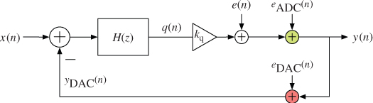
Figure 1.25 conceptually illustrates the parallel architecture that is typically used for the multibit quantizer in ![]() Ms, in which the resolution is usually low (
Ms, in which the resolution is usually low (![]() ). The
). The ![]() -bit ADC consists of a bank of
-bit ADC consists of a bank of ![]() comparators that digitizes the loop filter output into thermometer code, which will be subsequently coded into binary. The DAC employs
comparators that digitizes the loop filter output into thermometer code, which will be subsequently coded into binary. The DAC employs ![]() unit elements (capacitors, resistors, current sources, etc., depending on the circuit implementation) to reconstruct the analog feedback signal using
unit elements (capacitors, resistors, current sources, etc., depending on the circuit implementation) to reconstruct the analog feedback signal using ![]() levels (numbered from 0 to
levels (numbered from 0 to ![]() ). The
). The ![]() th analog output level is generated by activating
th analog output level is generated by activating ![]() unit elements and adding their outputs (charges or currents). DAC errors are caused by the mismatching between its unit elements, which makes the DAC output levels deviate from their nominal values. Assuming that the actual value of each unit element follows a Gaussian distribution, the worst-case relative error in the DAC output
unit elements and adding their outputs (charges or currents). DAC errors are caused by the mismatching between its unit elements, which makes the DAC output levels deviate from their nominal values. Assuming that the actual value of each unit element follows a Gaussian distribution, the worst-case relative error in the DAC output ![]() can be estimated as
can be estimated as
where ![]() stands for the relative error in the value of the unit element. Obviously, the DAC accuracy increases with the number of unit elements, thanks to the parallel topology. However, for a
stands for the relative error in the value of the unit element. Obviously, the DAC accuracy increases with the number of unit elements, thanks to the parallel topology. However, for a ![]() M with 4-bit embedded quantization to achieve 16-bit linearity, the required matching for the DAC unit elements should be better than
M with 4-bit embedded quantization to achieve 16-bit linearity, the required matching for the DAC unit elements should be better than ![]() (13 bits). Device matching achieved in present-day CMOS processes is nevertheless in the range of
(13 bits). Device matching achieved in present-day CMOS processes is nevertheless in the range of ![]() (10 bits) and the required accuracy in the elements can only be obtained through the parallel connection of many more of them (
(10 bits) and the required accuracy in the elements can only be obtained through the parallel connection of many more of them (![]() ). This means that achieving linearities better than 12 or 13 bits in multibit
). This means that achieving linearities better than 12 or 13 bits in multibit ![]() Ms by means of relying only on standard device matching usually leads to prohibitive area occupation.
Ms by means of relying only on standard device matching usually leads to prohibitive area occupation.
Figure 1.25 Parallel topology of a typical multibit quantizer embedded in a ![]() M.
M.

A direct method to improve the standard device matching is laser trimming, what can sometimes be done at the foundry, but at the expense of additional fabrication and/or measurement steps and increased cost. Calibration and correction schemes have also been proposed, either in analog or digital domain [58], but they are often expensive to implement in terms of system design complexity, hardware requirements, and power consumption.
Among the different alternatives that have been developed through the years for achieving high-linear multibit ![]() Ms, two of them clearly prevail because of the modest component matching required and the reduced circuit complexity involved. These approaches are discussed in the following text.
Ms, two of them clearly prevail because of the modest component matching required and the reduced circuit complexity involved. These approaches are discussed in the following text.
1.6.2 DEM Techniques
As previously discussed, mismatches among the unit elements cause DAC nonlinearities that generate harmonic distortion in the ![]() M. For a multibit DAC with the topology in Figure 1.25, there is a univocal correspondence between the thermometric input code (
M. For a multibit DAC with the topology in Figure 1.25, there is a univocal correspondence between the thermometric input code (![]() ) and the respective error of the DAC output(
) and the respective error of the DAC output(![]() ), because the same unit elements are always used for generating a given DAC output level. The operation principle of DEM consists in breaking this direct correspondence by varying over time the set of elements that are employed for generating a given DAC level, thus transforming its fixed error into a time-varying one. To that purpose, as conceptually illustrated in Figure 1.26, a digital block is incorporated, which controls the selection of unit elements at each clock cycle according to an algorithm that tries to null the average error in each DAC level over time. This way, part of the DAC error power that lies in the low-frequency range will thus be pushed to higher frequencies and removed by the decimator.
), because the same unit elements are always used for generating a given DAC output level. The operation principle of DEM consists in breaking this direct correspondence by varying over time the set of elements that are employed for generating a given DAC level, thus transforming its fixed error into a time-varying one. To that purpose, as conceptually illustrated in Figure 1.26, a digital block is incorporated, which controls the selection of unit elements at each clock cycle according to an algorithm that tries to null the average error in each DAC level over time. This way, part of the DAC error power that lies in the low-frequency range will thus be pushed to higher frequencies and removed by the decimator.
Figure 1.26 Incorporating an element selection logic for applying DEM to a multibit DAC.

The incorporation of DEM techniques to multibit ![]() Ms is facilitated by digitally oriented CAD tools and can represent a little area overhead in the current CMOS process, what explains the large number of algorithms that have been developed though the years. A detailed overview of many of them can be found in [9, 58, 59]. They can be categorized as follows:
Ms is facilitated by digitally oriented CAD tools and can represent a little area overhead in the current CMOS process, what explains the large number of algorithms that have been developed though the years. A detailed overview of many of them can be found in [9, 58, 59]. They can be categorized as follows:
- Randomization Algorithms, in which the DAC unit elements are selected according to pseudo-randomly configured networks (e.g., butterfly structures) [60]. Harmonic distortion induced by the DAC is transformed into white noise, whose out-of-band power will be removed by the decimation filter. The DAC error power lying within the signal band will nevertheless increase the noise floor of the
 M.
M. - Rotation Algorithms, in which the DAC unit elements are selected in a periodic manner for shifting harmonic distortion out of the signal band. The
 M noise floor is not increased, but the signal processing can originate mixed frequency components that fold over the modulator passband. Clocked averaging (CLA) [61] is an example of this kind of DEM techniques.
 - Mismatch-Shaping Algorithms, in which the DAC unit elements are selected according to algorithms that conform the mismatching error to push most of its power to higher frequencies. The order of the mismatch shaping is normally limited to one or two. Individual level averaging (ILA) [62] and data weighted averaging (DWA) [63]—and its many modifications—pertain to this kind of algorithms.
- Vector-Quantizer Structures, in which a digital
 converter in error-feedback configuration is incorporated to achieve high-order shaping [64].
DWA and Pseudo-DWA Algorithms
Among the many different DEM alternatives, DWA [63]—or a modified version of DWA—dominates in high-speed, high-resolution ![]() modulators with multibit quantization. In such high-speed
modulators with multibit quantization. In such high-speed ![]() Ms, the complexity of the DEM algorithm becomes a concern because the delay introduced by the DEM selection logic in the
Ms, the complexity of the DEM algorithm becomes a concern because the delay introduced by the DEM selection logic in the ![]() feedback loop can limit the maximum achievable clock frequency. Regarding this, DWA results in highly practical implementations, especially when the number of DAC elements is large [59].
feedback loop can limit the maximum achievable clock frequency. Regarding this, DWA results in highly practical implementations, especially when the number of DAC elements is large [59].
Consider an ![]() -element DAC, as that shown in Figure 1.26, with input code
-element DAC, as that shown in Figure 1.26, with input code ![]() . In conventional DWA [63], the DAC unit elements are selected sequentially from the DAC array beginning with the next available unused element. An index pointer
. In conventional DWA [63], the DAC unit elements are selected sequentially from the DAC array beginning with the next available unused element. An index pointer ![]() stores the address of that element in a digital register and governs the rotational element selection process, so that the DAC elements selected at time
stores the address of that element in a digital register and governs the rotational element selection process, so that the DAC elements selected at time ![]() are those from
are those from ![]() to
to ![]() by increasing order. Every clock cycle, the index pointer is incremented modulus
by increasing order. Every clock cycle, the index pointer is incremented modulus ![]() by the DAC input code
by the DAC input code ![]() according to
according to
Figure 1.27 illustrates how the elements of a 4-bit DAC would be selected following the DWA algorithm given earlier, which achieves a first-order shaping of the DAC mismatch errors.
Figure 1.27 Selection of unit elements in a 15-element DAC according to the DWA algorithm in Equation 1.49. The shaded boxes indicate the elements that contribute to generate the DAC output level ![]() for the corresponding input code
for the corresponding input code ![]() .
.

However, if the ![]() M input is DC or varies slowly, and there is a rational relation between its value and the number of DAC elements, out-of-band tones are generated that may fold back to the signal band due to the modulation by the
M input is DC or varies slowly, and there is a rational relation between its value and the number of DAC elements, out-of-band tones are generated that may fold back to the signal band due to the modulation by the ![]() M's output waveform [63]. Several modifications of the conventional DWA algorithm have been proposed to reduce its tonal behavior, such as rotated data weighted averaging (R-DWA) [65], randomized data weighted averaging (Rn-DWA) [66], bidirectional data weighted averaging (Bi-DWA) [67], partitioned data weighted averaging (P-DWA) [51], and pseudo DWA [68].
M's output waveform [63]. Several modifications of the conventional DWA algorithm have been proposed to reduce its tonal behavior, such as rotated data weighted averaging (R-DWA) [65], randomized data weighted averaging (Rn-DWA) [66], bidirectional data weighted averaging (Bi-DWA) [67], partitioned data weighted averaging (P-DWA) [51], and pseudo DWA [68].
Among them, pseudo DWA significantly decreases the tonal power with a minor modification of the DWA algorithm. Pseudo DWA modifies the DWA scheme by inverting with periodicity ![]() the least-significant bit (LSB) of the DAC input code
the least-significant bit (LSB) of the DAC input code ![]() used to update the index pointer in Equation 1.49. The element-selection process is thus essentially the same as in conventional DWA except that, in every
used to update the index pointer in Equation 1.49. The element-selection process is thus essentially the same as in conventional DWA except that, in every ![]() clock cycle, a DAC element is either reselected or skipped depending on whether the previous DAC input code was odd or even, respectively. This modification of the DWA algorithm breaks the cyclic nature of the element-selection process and, hence, reduces the tonal behavior [68]. The choice of
clock cycle, a DAC element is either reselected or skipped depending on whether the previous DAC input code was odd or even, respectively. This modification of the DWA algorithm breaks the cyclic nature of the element-selection process and, hence, reduces the tonal behavior [68]. The choice of ![]() is, however, a compromise between linearity and resolution. If
is, however, a compromise between linearity and resolution. If ![]() is too large—note that
is too large—note that ![]() corresponds to conventional DWA—the signal-dependent tones will not be eliminated. If
corresponds to conventional DWA—the signal-dependent tones will not be eliminated. If ![]() is too small, different DAC elements will be used at significantly different rates, what results in an increase of the in-band noise. Deriving an analytical expression for the optimum value of
is too small, different DAC elements will be used at significantly different rates, what results in an increase of the in-band noise. Deriving an analytical expression for the optimum value of ![]() is rather complex, but simple behavioral simulations can be used to find an appropriate value for a given multibit
is rather complex, but simple behavioral simulations can be used to find an appropriate value for a given multibit ![]() M [68].
M [68].
1.6.3 Dual Quantization
Rather than reducing the DAC mismatch errors that are injected in the feedback of a multibit ![]() M—as DEM techniques do—dual quantization basically consists in injecting them at a different point, where their influence on the overall
M—as DEM techniques do—dual quantization basically consists in injecting them at a different point, where their influence on the overall ![]() M linearity is not severe. The operation principle of dual quantization is to employ both single- and multibit quantization at a time in a
M linearity is not severe. The operation principle of dual quantization is to employ both single- and multibit quantization at a time in a ![]() M: two-level quantization for its intrinsic linearity and multibit quantization for its reduced error power. The concept is applicable to both single-loop and cascade
M: two-level quantization for its intrinsic linearity and multibit quantization for its reduced error power. The concept is applicable to both single-loop and cascade ![]() Ms.
Ms.
Dual-Quantization Single-Loop  Ms
Ms
Figure 1.28 shows a third-order, single-loop ![]() M with dual quantization [69], in which the first two integrators are fed by a two-level DAC, whereas the third one is fed by a multibit DAC. The outputs of the corresponding ADCs are digitally processed to cancel the coarse 1-bit quantization error at the overall output, in which only the fine multibit quantization error ideally remains. The modulator linearity is not menaced, as DAC mismatch errors are suppressed by the gain of the first two integrators and are thus second-order, high-pass shaped. The third-order
M with dual quantization [69], in which the first two integrators are fed by a two-level DAC, whereas the third one is fed by a multibit DAC. The outputs of the corresponding ADCs are digitally processed to cancel the coarse 1-bit quantization error at the overall output, in which only the fine multibit quantization error ideally remains. The modulator linearity is not menaced, as DAC mismatch errors are suppressed by the gain of the first two integrators and are thus second-order, high-pass shaped. The third-order ![]() M also benefits from improved stability thanks to the multibit feedback in the back-end integrator. Note that the topology, however, requires a DCL and thus suffers from noise leakages.
M also benefits from improved stability thanks to the multibit feedback in the back-end integrator. Note that the topology, however, requires a DCL and thus suffers from noise leakages.
Figure 1.28 A third-order single-loop ![]() M employing dual quantization [69].
M employing dual quantization [69].
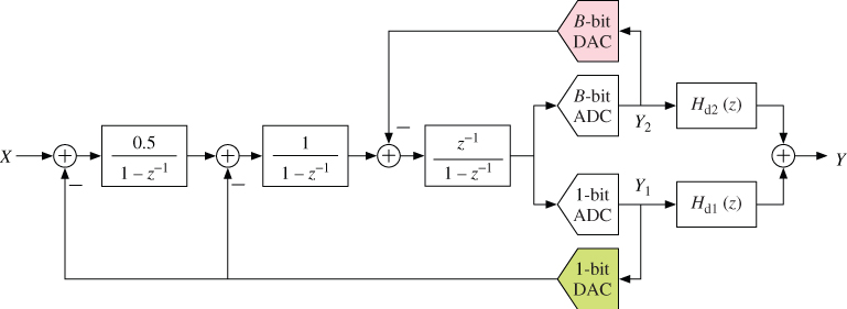
The concept in Figure 1.28 can be generalized to higher-order ![]() Ms. As the order of the loop filter increases, the number of back-end integrators with multibit feedback is a trade-off between aggressive noise shaping (to improve stability) and linearity requirements of the multibit DAC.
Ms. As the order of the loop filter increases, the number of back-end integrators with multibit feedback is a trade-off between aggressive noise shaping (to improve stability) and linearity requirements of the multibit DAC.
Dual-Quantization Cascade  Ms
Ms
Dual-quantization schemes are naturally incorporated to cascade ![]() Ms [70]. As shown in Section 1.5, the output of a cascade
Ms [70]. As shown in Section 1.5, the output of a cascade ![]() M ideally contains only the input signal and the last-stage quantization error, whereas the quantization errors from the remaining stages are removed by the DCL. The DR of the
M ideally contains only the input signal and the last-stage quantization error, whereas the quantization errors from the remaining stages are removed by the DCL. The DR of the ![]() M can be thus easily increased using multibit quantization only in the back-end stage. The remaining quantizers can be single-bit ones to retain linear feedback in the front-end stages. Therefore, the resulting topology is that illustrated in Figure 1.21 with
M can be thus easily increased using multibit quantization only in the back-end stage. The remaining quantizers can be single-bit ones to retain linear feedback in the front-end stages. Therefore, the resulting topology is that illustrated in Figure 1.21 with ![]() and
and ![]() . This way, nonlinearities in the multibit DAC will appear at the overall cascade output with a shaping of order equal to the summation of the order of the preceding
. This way, nonlinearities in the multibit DAC will appear at the overall cascade output with a shaping of order equal to the summation of the order of the preceding ![]() stages, so that Equation 1.43 yields
stages, so that Equation 1.43 yields

if the error in the back-end multibit DAC ![]() is taken into account in the linear analysis. Many cascade
is taken into account in the linear analysis. Many cascade ![]() M integrated circuits using this dual-quantization scheme can be found in the literature [4, 10, 18].
M integrated circuits using this dual-quantization scheme can be found in the literature [4, 10, 18].
Many cascade ![]() Ms employing multibit quantization in all stages have also been reported [51, 67]. Note that, under ideal conditions, the quantization errors of all but the last stage are canceled at the overall cascade output by the DCL. Multibit quantization can be used in these stages with a twofold purpose as follows:
Ms employing multibit quantization in all stages have also been reported [51, 67]. Note that, under ideal conditions, the quantization errors of all but the last stage are canceled at the overall cascade output by the DCL. Multibit quantization can be used in these stages with a twofold purpose as follows:
- For reducing the power of the respective quantization errors that will in practice leak to the output. DEM techniques can be employed in the front-end
 stage for achieving the targeted modulator linearity, whereas the remaining multibit stages often rely just on the shaping provided by the preceding integrators [51].
 - For increasing the value of the interstage scaling coefficients
 in the
  cascade—see Figure 1.21—in comparison with a 1-bit approach, while avoiding overloading [67]. This way, the factor
  that amplifies the last-stage quantization error in Equation 1.50can be made smaller than unity, what increases the DR over that ideally attainable with an
  th-order
  -bit
-bit  M.
M.
Cascade ![]() Ms using trilevel (1.5-bit) quantizers [53] are also often employed, as they yield a 3-dB reduction of the quantization error power compared to 1-bit quantization. Although trilevel coding is not inherently linear, it is often used in fully-differential SC
Ms using trilevel (1.5-bit) quantizers [53] are also often employed, as they yield a 3-dB reduction of the quantization error power compared to 1-bit quantization. Although trilevel coding is not inherently linear, it is often used in fully-differential SC ![]() Ms, because highly linear trilevel DACs can be easily implemented using just one extra switch [71].
Ms, because highly linear trilevel DACs can be easily implemented using just one extra switch [71].
1.7 Band-Pass  Modulators
The operation principle of low-pass ![]() modulators (LP-
modulators (LP-![]() Ms)—in which the quantization noise is high-pass shaped for its suppression around DC—can be extended to the more general case of stop-band filtering of the quantization noise for its suppression around a nonzero frequency in a so-called band-pass
Ms)—in which the quantization noise is high-pass shaped for its suppression around DC—can be extended to the more general case of stop-band filtering of the quantization noise for its suppression around a nonzero frequency in a so-called band-pass ![]() modulator (BP-
modulator (BP-![]() M) [72, 73]. A direct application of this band-pass approach can be found in the A/D conversion of many wireless receiver systems, in which a BP-
M) [72, 73]. A direct application of this band-pass approach can be found in the A/D conversion of many wireless receiver systems, in which a BP-![]() M is used for the digitization of intermediate frequency (IF) signals [18, 74].9 Although a broadband Nyquist-rate ADC could a priori be an alternative to BP-
M is used for the digitization of intermediate frequency (IF) signals [18, 74].9 Although a broadband Nyquist-rate ADC could a priori be an alternative to BP-![]() Ms for the digitization in IF-conversion receivers, the bandwidth of IF signals is typically much smaller than the carrier frequency and the reduction of the quantization noise over the entire Nyquist band thus becomes very inefficient. Instead, if a BP-
Ms for the digitization in IF-conversion receivers, the bandwidth of IF signals is typically much smaller than the carrier frequency and the reduction of the quantization noise over the entire Nyquist band thus becomes very inefficient. Instead, if a BP-![]() M is used, the quantization noise is attenuated only in a narrowband around the IF location, thus taking advantage of a high OSR to achieve high DR requirements, even in the presence of strong interfering signals.
M is used, the quantization noise is attenuated only in a narrowband around the IF location, thus taking advantage of a high OSR to achieve high DR requirements, even in the presence of strong interfering signals.
Figure 1.29 illustrates a typical block diagram of the IF-to-baseband section in a digital receiver based on a BP-![]() M. As shown, the BP-
M. As shown, the BP-![]() M contains a BP loop filter
M contains a BP loop filter ![]() for obtaining a stop-band NTF with zeros placed at a nonzero frequency, often referred to as the notch frequency
for obtaining a stop-band NTF with zeros placed at a nonzero frequency, often referred to as the notch frequency ![]() . The digital output of the modulator is mixed to DC by a digital quadrature mixer and then LP filtered and decimated by a quadrature decimation filter to remove out-of-band spectral components and quantization noise. The resulting baseband digital data are finally processed in a DSP.10
. The digital output of the modulator is mixed to DC by a digital quadrature mixer and then LP filtered and decimated by a quadrature decimation filter to remove out-of-band spectral components and quantization noise. The resulting baseband digital data are finally processed in a DSP.10
Figure 1.29 Typical section of an IF-conversion receiver based on a BP ![]() ADC. For the sake of illustration, the input IF frequency
ADC. For the sake of illustration, the input IF frequency ![]() is assumed to be
is assumed to be ![]() and a notch frequency
and a notch frequency ![]() is assumed in the BP-
is assumed in the BP-![]() M and in the quadrature digital mixer.
M and in the quadrature digital mixer.

Note that an LP-![]() M has its NTF zeros at or near
M has its NTF zeros at or near ![]() (which corresponds to DC), whereas those of a BP-
(which corresponds to DC), whereas those of a BP-![]() M are placed elsewhere on the unit circle; that is,
M are placed elsewhere on the unit circle; that is, ![]() (which corresponds to
(which corresponds to ![]() , with
, with ![]() ). As the NTF zeros occur in complex conjugate pairs, realizing
). As the NTF zeros occur in complex conjugate pairs, realizing ![]() zeros of the NTF in the passband of a BP-
zeros of the NTF in the passband of a BP-![]() M thus requires a
M thus requires a ![]() th-order BP loop filter. In other words, the shaping performed on the quantization noise by a
th-order BP loop filter. In other words, the shaping performed on the quantization noise by a ![]() th-order BP-
th-order BP-![]() M is equivalent to that performed by an
M is equivalent to that performed by an ![]() th-order LP-
th-order LP-![]() M.
M.
1.7.1 The  LP–BP Transformation
A common design choice for the notch frequency of a BP-![]() M is
M is ![]() , because this location optimizes the trade-off between antialiasing filtering and image-rejection filtering in digital radio receivers [74]. It also helps to simplify the quadrature digital mixer to baseband, as the general digital cosine and sine sequences (
, because this location optimizes the trade-off between antialiasing filtering and image-rejection filtering in digital radio receivers [74]. It also helps to simplify the quadrature digital mixer to baseband, as the general digital cosine and sine sequences (![]() ) reduce to a quadrature data series of
) reduce to a quadrature data series of ![]() s,
s, ![]() s, and
s, and ![]() s, as illustrated in Figure 1.29. More importantly, the NTF zeros of a so-called
s, as illustrated in Figure 1.29. More importantly, the NTF zeros of a so-called ![]() BP-
BP-![]() M are placed at
M are placed at ![]() , so that the synthesis of the BP
, so that the synthesis of the BP ![]() loop filter can be easily derived from an initial LP prototype by applying the transformation
loop filter can be easily derived from an initial LP prototype by applying the transformation
1.51 ![]()
which is often referred to as the ![]() LP–BP transformation of
LP–BP transformation of ![]() modulators.
modulators.
This transformation is exemplary applied in Figure 1.30 to a second-order LP-![]() M to obtain a fourth-order
M to obtain a fourth-order ![]() BP-
BP-![]() M, in which the integrators are replaced by resonators. The resulting BP architecture preserves all properties of its LP original concerning dynamics, stability, resolution, etc. Indeed, it can be shown that the main performance figures (IBN, SNR, DR, etc.) of
M, in which the integrators are replaced by resonators. The resulting BP architecture preserves all properties of its LP original concerning dynamics, stability, resolution, etc. Indeed, it can be shown that the main performance figures (IBN, SNR, DR, etc.) of ![]() BP-
BP-![]() Ms have the same expressions as the ones derived in previous sections for the LP case. For the sake of illustration, if the
Ms have the same expressions as the ones derived in previous sections for the LP case. For the sake of illustration, if the ![]() transformation is applied to the NTF of an ideal
transformation is applied to the NTF of an ideal ![]() th-order LP
th-order LP ![]() M in Equation 1.21, that resulting for an ideal
M in Equation 1.21, that resulting for an ideal ![]() th-order BP
th-order BP ![]() M yields
M yields
1.52 ![]()
Figure 1.30 Illustration of the ![]() LP–BP transformation of
LP–BP transformation of ![]() Ms: (a) block diagram of a second-order LP-
Ms: (a) block diagram of a second-order LP-![]() M, (b) block diagram of the resulting fourth-order
M, (b) block diagram of the resulting fourth-order ![]() BP-
BP-![]() M, (c) zero-pole plot of the NTF of the LP-
M, (c) zero-pole plot of the NTF of the LP-![]() M, (d) zero-pole plot of the NTF of the BP-
M, (d) zero-pole plot of the NTF of the BP-![]() M, (e) output spectrum of the LP-
M, (e) output spectrum of the LP-![]() M (
M (![]() , and (f) output spectrum of the BP-
, and (f) output spectrum of the BP-![]() M (
M (![]() .
.
By integrating the shaped quantization noise over the signal band, the resulting IBN is obtained to be
1.53 
so that the expression equals that of the LP case in Equation 1.12.
However, centering the signal passband at ![]() has some disadvantages. On the one hand, in the presence of nonlinearities in the analog circuitry of the
has some disadvantages. On the one hand, in the presence of nonlinearities in the analog circuitry of the ![]() M, any intermodulation distortion products resulting from the mixing of tones at
M, any intermodulation distortion products resulting from the mixing of tones at ![]() with the input signal will fall inside the modulator passband and will thus corrupt the signal information. On the other, for a given input IF, the clock rate demands are more restrictive than placing
with the input signal will fall inside the modulator passband and will thus corrupt the signal information. On the other, for a given input IF, the clock rate demands are more restrictive than placing ![]() between
between ![]() and
and ![]() .11
.11
1.7.2 BP- Ms with Optimized NTF
In practice, the ![]() transformation was commonly used, but many more custom-designed loop filters are nowadays reported, in which the synthesis of the optimized STF and NTF is directly addressed through the proper placement of their poles and zeros [82–84]—this is especially the case if the loop filter has to show special characteristics, such as adjacent-channel suppression or partial mixing inside the
transformation was commonly used, but many more custom-designed loop filters are nowadays reported, in which the synthesis of the optimized STF and NTF is directly addressed through the proper placement of their poles and zeros [82–84]—this is especially the case if the loop filter has to show special characteristics, such as adjacent-channel suppression or partial mixing inside the ![]() M [16, 22, 23]. In this respect, BP-
M [16, 22, 23]. In this respect, BP-![]() Ms exhibit the same architectural variety as LP-
Ms exhibit the same architectural variety as LP-![]() Ms and the trade-offs between the different structures are also essentially the same [18]. BP modulators can be implemented using either single-loopor cascade topologies, with a similar trade-off between improved stability and increased sensitivity to noise leakages due to nonidealities in the analog circuitry. Similarly, the loop filter of BP-
Ms and the trade-offs between the different structures are also essentially the same [18]. BP modulators can be implemented using either single-loopor cascade topologies, with a similar trade-off between improved stability and increased sensitivity to noise leakages due to nonidealities in the analog circuitry. Similarly, the loop filter of BP-![]() Ms can be implemented using any of the topologies commonly employed for LP-
Ms can be implemented using any of the topologies commonly employed for LP-![]() Ms, such as the feedback, feed-forward, and hybrid topologies shown in Figures 1.19, and 1.20, respectively.
Ms, such as the feedback, feed-forward, and hybrid topologies shown in Figures 1.19, and 1.20, respectively.
Figure 1.31 shows two architectural alternatives for the implementation of a fourth-order BP-![]() M, which allow the optimization of both STF and NTF. The BP architecture in Figure 1.31a is based on the LP-
M, which allow the optimization of both STF and NTF. The BP architecture in Figure 1.31a is based on the LP-![]() M with distributed feedback in Figure 1.18, whereas that in Figure 1.31b is based on the LP-
M with distributed feedback in Figure 1.18, whereas that in Figure 1.31b is based on the LP-![]() M with feed-forward summation in Figure 1.19. Both band-pass topologies include input feed forward for eliminating the input-signal content from the loop filter and thus relaxing the requirements of the analog circuitry [29]. In addition, if designed properly, input feed forward flattens the STF to a constant without any peaking, what prevents undesirable amplification of out-of-band interferers [18].
M with feed-forward summation in Figure 1.19. Both band-pass topologies include input feed forward for eliminating the input-signal content from the loop filter and thus relaxing the requirements of the analog circuitry [29]. In addition, if designed properly, input feed forward flattens the STF to a constant without any peaking, what prevents undesirable amplification of out-of-band interferers [18].
Figure 1.31 Illustration of fourth-order BP ![]() topologies that allow the NTF optimization: (a) cascade of resonators with feedback and (b) cascade of resonators with feed-forward summation.
topologies that allow the NTF optimization: (a) cascade of resonators with feedback and (b) cascade of resonators with feed-forward summation.

Note from Figure 1.31 that the BP loop filters are obtained by shifting the poles from DC to nonzero frequencies by adding internal feedback paths (coefficients ![]() ) in the initial LP topologies. Figure 1.32a depicts the lossless discrete integrator (LDI) loop that builds the resonator,12 which may be implemented using SC techniques as shown in Figure 1.32b. The transfer function of the LDI resonator is given by
) in the initial LP topologies. Figure 1.32a depicts the lossless discrete integrator (LDI) loop that builds the resonator,12 which may be implemented using SC techniques as shown in Figure 1.32b. The transfer function of the LDI resonator is given by
1.54 ![]()
so that the poles are ![]() . Note that, for
. Note that, for ![]() , the poles of RTF lie on the unit circle, and thus the quality factor
, the poles of RTF lie on the unit circle, and thus the quality factor ![]() of the resonator is ideally infinite.13 The resonant frequency of a resonator corresponds to a notch in the NTF of the BP-
of the resonator is ideally infinite.13 The resonant frequency of a resonator corresponds to a notch in the NTF of the BP-![]() M at a frequency
M at a frequency
1.55 ![]()
which can thus be placed at any arbitrary position from 0 to ![]() depending on the value of
depending on the value of ![]() —which is determined in an SC implementation by a capacitor ratio (Figure 1.32b).
—which is determined in an SC implementation by a capacitor ratio (Figure 1.32b).
Figure 1.32 Illustration of an LDI resonator: (a) block diagram and (b) SC implementation. Only half of the differential circuit is explicitly shown for the sake of simplicity.
Therefore, the center frequency of a BP-![]() M can be made programmable
M can be made programmable
by changing the resonant frequency of its resonators [85]—for example, by using programmable banks of capacitors for the SC implementation of coefficients ![]() . This feature is commonly exploited in digital radios, as the same programmable BP-
. This feature is commonly exploited in digital radios, as the same programmable BP-![]() M can be used for the digitization of different IF frequencies.14
M can be used for the digitization of different IF frequencies.14
1.8 Continuous-Time  Modulators
The majority of ![]() Ms reported up to recent years were implemented using DT circuit techniques, mostly based on SC circuits. However, the increasing demand for ever faster ADCs in broadband communication systems has raised the interest in CT-
Ms reported up to recent years were implemented using DT circuit techniques, mostly based on SC circuits. However, the increasing demand for ever faster ADCs in broadband communication systems has raised the interest in CT-![]() Ms over the past years, as they are able to operate at higher sampling rates with lower power consumption than their DT counterparts [16, 20, 75].
Ms over the past years, as they are able to operate at higher sampling rates with lower power consumption than their DT counterparts [16, 20, 75].
Figure 1.33 illustrates the general block diagram of a CT-![]() M for the case of LP input signals. To facilitate the direct comparison with DT implementations, the same partitioning as in Figure 1.7 has been adopted.
M for the case of LP input signals. To facilitate the direct comparison with DT implementations, the same partitioning as in Figure 1.7 has been adopted.
Figure 1.33 General block diagram of a continuous-time ![]() ADC. A low-pass
ADC. A low-pass ![]() M is assumed.
M is assumed.
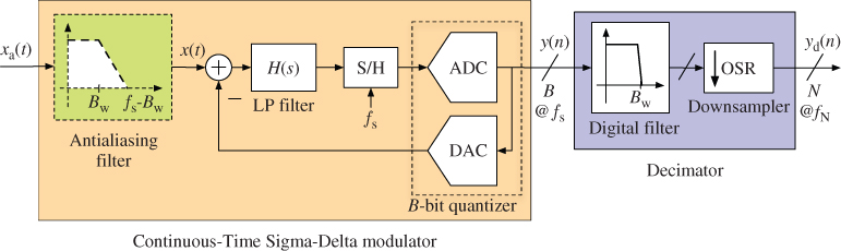
Looking at both figures, several differences are clearly visible between DT- and CT-![]() Ms. The most significant one is related to the location of the sampling operation, which moves from the modulator input in DT-
Ms. The most significant one is related to the location of the sampling operation, which moves from the modulator input in DT-![]() Ms to the point before the quantizer in CT-
Ms to the point before the quantizer in CT-![]() Ms. The loop filter can thus be realized using CT circuit techniques, but, given that the modulator output is a DT signal and the modulator input is a CT signal, a discrete-to-continuous time (DT–CT) transformation is required in CT-
Ms. The loop filter can thus be realized using CT circuit techniques, but, given that the modulator output is a DT signal and the modulator input is a CT signal, a discrete-to-continuous time (DT–CT) transformation is required in CT-![]() Ms to create the feedback signal. This can be better visualized comparing the signal processing involved in the block diagrams in Figures 1.34a and 1.34b.
Ms to create the feedback signal. This can be better visualized comparing the signal processing involved in the block diagrams in Figures 1.34a and 1.34b.
Figure 1.34 Conceptual block diagrams of ![]() Ms: (a) DT modulator, (b) CT modulator, (c) open-loop representation of a DT-
Ms: (a) DT modulator, (b) CT modulator, (c) open-loop representation of a DT-![]() M, and (d) open-loop representation of a CT-
M, and (d) open-loop representation of a CT-![]() M.
M.
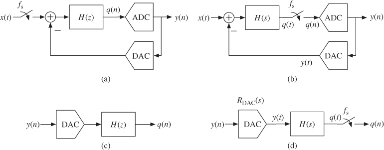
The reconstruction of the modulator output signal is very critical in CT-![]() Ms and has a significant impact on the overall modulator behavior [87]. There are a number of DAC waveforms that can be used in CT-
Ms and has a significant impact on the overall modulator behavior [87]. There are a number of DAC waveforms that can be used in CT-![]() Ms. Figure 1.35 shows a summary of the most representative possibilities, including the nomenclature used for the feedback waveforms extracted from [20]. Among others, the most commonly used DACs incorporate rectangular feedback pulses of basically three types: nonreturn-to-zero (NRZ) (Figure 1.35a), return-to-zero (RZ) (Figure 1.35b), and half-delay return-to-zero (HRZ) (Figure 1.35c). The DAC impulse response of these rectangular pulses can thus be globally expressed as
Ms. Figure 1.35 shows a summary of the most representative possibilities, including the nomenclature used for the feedback waveforms extracted from [20]. Among others, the most commonly used DACs incorporate rectangular feedback pulses of basically three types: nonreturn-to-zero (NRZ) (Figure 1.35a), return-to-zero (RZ) (Figure 1.35b), and half-delay return-to-zero (HRZ) (Figure 1.35c). The DAC impulse response of these rectangular pulses can thus be globally expressed as

where ![]() equals
equals ![]() ,
, ![]() , and
, and ![]() for NRZ, RZ, and HRZ DACs, respectively. Their Laplace
for NRZ, RZ, and HRZ DACs, respectively. Their Laplace ![]() -transforms can also be generally written as
-transforms can also be generally written as
Figure 1.35 Most common DAC impulse responses: (a) nonreturn-to-zero (NRZ), (b) return-to-zero (RZ), (c) half-delay return-to-zero (HRZ), (d) switched capacitor (SC), (e) exponential slope, and (f) cosine.

Although they combine DT and CT signals, modulators fitting into the architecture in Figure 1.34b are generically considered as CT-![]() Ms. Owing to the combination of both types of dynamics, together with the intrinsic nonlinearity associated to quantization, the mathematical analysis of CT-
Ms. Owing to the combination of both types of dynamics, together with the intrinsic nonlinearity associated to quantization, the mathematical analysis of CT-![]() Ms becomes more difficult than in the case of DT-
Ms becomes more difficult than in the case of DT-![]() Ms [16, 20, 75, 84, 87]. However, they present several pros compared to DT-
Ms [16, 20, 75, 84, 87]. However, they present several pros compared to DT-![]() Ms, such as15
Ms, such as15
- An explicit AAF can be avoided (Figure 1.33). As the sampling operation takes place before the quantizer, the resulting STF is affected by a
 function [24]. This sinc characteristic attenuates the signal spectrum exactly at multiples of the sampling frequency and thus leads to an implicit AAF
in CT-
function [24]. This sinc characteristic attenuates the signal spectrum exactly at multiples of the sampling frequency and thus leads to an implicit AAF
in CT- Ms.
Ms. - Errors associated to the sampling process have less impact on the modulator performance. As the sampling operation takes place before the quantizer, the resulting errors attenuate in a similar way as the quantization error does.
- There is no settling error associated to the loop filter circuitry. As will be shown in Chapter 2, signals in DT circuits must settle to their steady-state values within a given accuracy, because complete settling would require infinite time.
- The operation speed is larger. This is inherent to the operation of CT circuits, in which the circuit dynamics is not a parasitic such as in DT circuits, but a design primitive.
- They are not affected by
 noise as SC-
 Ms do.
1.8.1 DT–CT Transformation of  Ms
Ms
In the past, most work on ![]() Ms was focused on DT implementations, and great collective effort was made to develop innovative architectures, accurate models, and design and simulation CAD tools for DT-
Ms was focused on DT implementations, and great collective effort was made to develop innovative architectures, accurate models, and design and simulation CAD tools for DT-![]() Ms. Therefore, a straightforward procedure for designing CT-
Ms. Therefore, a straightforward procedure for designing CT-![]() Ms comes from considering an equivalent DT loop filter as a starting point, designing the DT-
Ms comes from considering an equivalent DT loop filter as a starting point, designing the DT-![]() M to meet the required performance, and then applying a DT–CT transformation.
M to meet the required performance, and then applying a DT–CT transformation.
The Impulse-Invariant Transformation
Let us consider again the block diagram of DT- and CT-![]() Ms in Figures 1.34a and b, respectively, and the signal processing involved. The underlying principle of the DT–CT transformation consists in achieving the equivalence of both modulators by imposing that the input of the quantizers are the same at the sampling instants; that is,
Ms in Figures 1.34a and b, respectively, and the signal processing involved. The underlying principle of the DT–CT transformation consists in achieving the equivalence of both modulators by imposing that the input of the quantizers are the same at the sampling instants; that is,
If this condition is met, the output bitstreams of both modulators and the noise performance would thus be identical. As illustrated in Figures 1.34c and d, the condition in Equation 1.58 can be translated into an equivalence of the input–output signal processing that is performed in both ![]() Ms in open-loop configuration, which yields
Ms in open-loop configuration, which yields
where ![]() and
and ![]() stand for the inverse
stand for the inverse ![]() - and
- and ![]() -transform operators,respectively, and
-transform operators,respectively, and ![]() stands for the CT transfer function of the DAC (see Equation 1.57 for the case of rectangular waveforms). In the time domain, this leads to the condition
stands for the CT transfer function of the DAC (see Equation 1.57 for the case of rectangular waveforms). In the time domain, this leads to the condition
1.60 
where ![]() stands for the convolution operator and
stands for the convolution operator and ![]() stands for the impulse response of the specific DAC (Equation 1.56 for rectangular waveforms). This transformation between DT and CT domain is known as the invariant-impulse transformation (IIT), because it makes the open-loop impulse responses of both
stands for the impulse response of the specific DAC (Equation 1.56 for rectangular waveforms). This transformation between DT and CT domain is known as the invariant-impulse transformation (IIT), because it makes the open-loop impulse responses of both ![]() Ms equal at the sampling instants.
Ms equal at the sampling instants.
On the basis of the IIT in Equation 1.59, the most usual procedure to design CT-![]() Ms consists of: first, matching the equivalent filter
Ms consists of: first, matching the equivalent filter ![]() with a reference DT loop filter chosen to fulfill the specifications; then, solving for the coefficients of the CT loop filter
with a reference DT loop filter chosen to fulfill the specifications; then, solving for the coefficients of the CT loop filter ![]() with the specific DAC response considered; and, finally, implementing
with the specific DAC response considered; and, finally, implementing ![]() with CT techniques, usually based on Gm-C or active-RC techniques.16 In theory, any arbitrary
with CT techniques, usually based on Gm-C or active-RC techniques.16 In theory, any arbitrary ![]() M topology, either single-loop or cascade, can be synthesized this way.
M topology, either single-loop or cascade, can be synthesized this way.
The information compiled in Tables 1.3 and 1.4 for the equivalence of LP loop filter poles at DC (![]() ,
, ![]() ) in DT and CT domains is useful in such a methodology [20]. For general poles, the original table in [88] can be employed, which can also be useful for the design of BP CT-
) in DT and CT domains is useful in such a methodology [20]. For general poles, the original table in [88] can be employed, which can also be useful for the design of BP CT-![]() Ms. Finally, the use of these tables of equivalent poles is easy and can also be automated and, moreover, extended to other DAC impulse responses different from the rectangular waveforms, as done in [20].
Ms. Finally, the use of these tables of equivalent poles is easy and can also be automated and, moreover, extended to other DAC impulse responses different from the rectangular waveforms, as done in [20].
Table 1.3 CT equivalents of first-order to fourth-order DT low-pass loop filter poles for the rectangular feedback DAC pulses defined in equation 1.56 [20]
Table 1.4 DT Equivalents of first-order to fourth-order CT low-pass loop filter poles for the rectangular feedback DAC pulses defined in equation 1.56 [20]
DT–CT Transformation of a Second-Order  M
M
For the sake of illustration, Figure 1.36 shows a second-order CT-![]() M obtained using such a method from its DT equivalent in Figure 1.15a. Note from the former figure that the DT integrators—with transfer function given by Equation 1.16—are transformed into CT integrators with unscaled transfer functions given by
M obtained using such a method from its DT equivalent in Figure 1.15a. Note from the former figure that the DT integrators—with transfer function given by Equation 1.16—are transformed into CT integrators with unscaled transfer functions given by
1.61 ![]()
and that the scaling coefficients ![]() of the CT-
of the CT-![]() M are associated to the feedback paths [20]. This notation has been adopted because it can easily account for some nonidealities in the loop filter, as will be shown in Chapter 2. Note from Figure 1.36 that the discrimination of the signal scaling coefficient
M are associated to the feedback paths [20]. This notation has been adopted because it can easily account for some nonidealities in the loop filter, as will be shown in Chapter 2. Note from Figure 1.36 that the discrimination of the signal scaling coefficient ![]() and the first feedback scaling coefficient
and the first feedback scaling coefficient ![]() accounts for changing feedback coefficients when adopting DAC feedback pulses different from the rectangular NRZ [20]. Therefore, the input scaling coefficient remains equally constant to
accounts for changing feedback coefficients when adopting DAC feedback pulses different from the rectangular NRZ [20]. Therefore, the input scaling coefficient remains equally constant to ![]() regardless of the particular feedback waveform that is used.
regardless of the particular feedback waveform that is used.
Figure 1.36 Block diagram of a second-order CT-![]() M using the notation in [20].
M using the notation in [20].

The CT equivalent of the DT-![]() M in Figure 1.15a can be easily calculated by, on the one hand, applying the IIT in Equation 1.59 to the DT loop filter
M in Figure 1.15a can be easily calculated by, on the one hand, applying the IIT in Equation 1.59 to the DT loop filter
where an NRZ rectangular waveform has been exemplary assumed in the feedback DAC of the CT equivalent. To that purpose, rows 1 and 2 of Table 1.3 have been adopted considering ![]() . On the other hand, the CT loop filter in Figure 1.36 is obtained as
. On the other hand, the CT loop filter in Figure 1.36 is obtained as
Equating the CT coefficients in Equations 1.62 and 1.63 results in the following relations between the coefficients of the second-order DT-![]() M and the CT coefficients for the case of an NRZ DAC:
M and the CT coefficients for the case of an NRZ DAC:

The DT scaling coefficients ![]() typically used—see Table 1.1 and optimal coefficients reported in [8]—thus result in
typically used—see Table 1.1 and optimal coefficients reported in [8]—thus result in ![]() and
and ![]() .
.
For the sake of illustration, Figure 1.37 shows a possible implementation of the resulting CT-![]() M using active-RC integrators. Note that the corner frequency
M using active-RC integrators. Note that the corner frequency ![]() of an active-RC integrator is determined by the value of
of an active-RC integrator is determined by the value of ![]() , so that the scaling coefficients of the CT-
, so that the scaling coefficients of the CT-![]() M yield [20]:
M yield [20]:
1.65 ![]()
For the second-order CT-![]() M in Figures 1.36 and 1.37, the relations to be fulfilled for the correct implementation of the modulator coefficients are thus
M in Figures 1.36 and 1.37, the relations to be fulfilled for the correct implementation of the modulator coefficients are thus
1.66 
which, for the particular case of NRZ DAC considered, yield
1.67 
Figure 1.37 Active-RC implementation of a second-order CT-![]() M with a single-bit NRZ DAC.
M with a single-bit NRZ DAC.

1.8.2 Direct Synthesis of CT- Ms
Ms
The main problem of using the DT–CT transformation method given earlier is that it may yield an increase of complexity in the analog circuitry, with the subsequent penalty in sensitivity to variations on the technological process parameters. This is particularly critical in the case of CT cascades, where, to get a functional modulator while keeping the digital cancelation logic of the original DT-![]() M, every integrator and DAC output must be connected to the integrator input of later stages [20].
M, every integrator and DAC output must be connected to the integrator input of later stages [20].
An alternative method for designing the CT loop filter directly uses the desired ![]() as a starting point, just in the same way as described in Section 1.4.2 for synthesizing optimized NTFs in the DT case. This synthesis method is often referred to as direct CT synthesis method. Usually, an inverse Chebyshev distribution of the
as a starting point, just in the same way as described in Section 1.4.2 for synthesizing optimized NTFs in the DT case. This synthesis method is often referred to as direct CT synthesis method. Usually, an inverse Chebyshev distribution of the ![]() zeros is considered because it has advantages in terms of SNR and stability. Once the desired
zeros is considered because it has advantages in terms of SNR and stability. Once the desired ![]() has been chosen, the loop filter can be derived from the linearized model [16].
has been chosen, the loop filter can be derived from the linearized model [16].
It can be shown that applying the direct synthesis method to cascade CT-![]() Ms, more efficient architectures are obtained in terms of loop filter optimization, analog circuitry complexity, power consumption, and robustness to circuit element tolerance errors [89]. However, there are two major drawbacks to this method: first, previous knowledge of DT-
Ms, more efficient architectures are obtained in terms of loop filter optimization, analog circuitry complexity, power consumption, and robustness to circuit element tolerance errors [89]. However, there are two major drawbacks to this method: first, previous knowledge of DT-![]() Ms is not reused, which raises questions about stability; second, simulations are harder due to the fact that every simulation has to be done in CT.
Ms is not reused, which raises questions about stability; second, simulations are harder due to the fact that every simulation has to be done in CT.
1.9 Summary
This chapter has presented an introduction to ![]() ADCs. The benefits of employing oversampling and quantization noise shaping in the digitization of signals have been analyzed and compared to the performance of Nyquist-rate ADCs. Among the several blocks that build up an
ADCs. The benefits of employing oversampling and quantization noise shaping in the digitization of signals have been analyzed and compared to the performance of Nyquist-rate ADCs. Among the several blocks that build up an ![]() ADC, the chapter has focused on the
ADC, the chapter has focused on the ![]() modulator. Its general topology, ideal operation, and performance metrics have been presented.
modulator. Its general topology, ideal operation, and performance metrics have been presented.
The existing methods for increasing the effective resolution of an ![]() modulator have been discussed, presenting practical ways to implement stable high-order noise shaping topologies and to resort to multibit quantization. The DT and CT implementation of
modulator have been discussed, presenting practical ways to implement stable high-order noise shaping topologies and to resort to multibit quantization. The DT and CT implementation of ![]() modulators have been addressed, as well as their application to convert LP or BP signals. The implications of these different alternatives at the architectural and circuit levels have been presented in an incremental way, starting from the initial case of DT, LP single-bit modulators.
modulators have been addressed, as well as their application to convert LP or BP signals. The implications of these different alternatives at the architectural and circuit levels have been presented in an incremental way, starting from the initial case of DT, LP single-bit modulators.
These basic concepts have been discussed mainly considering the quantization noise as the only source of error limiting the resolution of an ![]() modulator. The effect of nonidealities associated with the practical circuit implementation of the modulator blocks will be analyzed in Chapter 2.
modulator. The effect of nonidealities associated with the practical circuit implementation of the modulator blocks will be analyzed in Chapter 2.
References
[1] W. Bennett, “Spectra of Quantized Signals,” Bell System Technical Journal, vol. 27, pp. 446–472, July 1948.
[2] B. Widrow, “Statistical Analysis of Amplitude-Quantized Sampled-Data Systems,” Transactions of the AIEE - Part II: Applications and Industry, vol. 79, pp. 555–568, January 1960.
[3] A. B. Sripad and D. L. Snyder, “A Necessary and Sufficient Condition for Quantization Errors to be Uniform and White,” IEEE Transactions on Acoustics, Speech and Signal Processing, vol. 25, pp. 442–448, October 1977.
[4] S. R. Norsworthy, R. Schreier, and G. C. Temes, Delta-Sigma Data Converters: Theory, Design and Simulation, IEEE Press, 1997.
[5] R. van de Plassche, CMOS Integrated Analog-to-Digital and Digital-to-Analog Converters, Springer, 2003.
[6] H. Inose, Y. Yasuda, and J. Murakami, “A Telemetering System by Code Modulation –![]() Modulation,” IRE Transactions on Space Electronics and Telemetry, vol. 8, pp. 204–209, September 1962.
Modulation,” IRE Transactions on Space Electronics and Telemetry, vol. 8, pp. 204–209, September 1962.
[7] B. E. Boser and B. A. Wooley, “The Design of Sigma-Delta Modulation Analog-to-Digital Converters,” IEEE Journal of Solid-State Circuits, vol. 23, pp. 1298–1308, December 1988.
[8] A. Marques, V. Peluso, M. S. Steyaert, and W. M. Sansen, “Optimal Parameters for ![]() Modulator Topologies,” IEEE Transactions on Circuits and Systems II: Analog and Digital Signal Processing, vol. 45, pp. 1232–1241, September 1998.
Modulator Topologies,” IEEE Transactions on Circuits and Systems II: Analog and Digital Signal Processing, vol. 45, pp. 1232–1241, September 1998.
[9] Y. Geerts, M. Steyaert, and W. Sansen, Design of Multi-bit Delta-Sigma A/D Converters, Kluwer Academic Publishers, 2002.
[10] A. Rodríguez-Vázquez, F. Medeiro, J. M. de la Rosa, R. del Río, R. Tortosa, and B. Pérez-Verdú, “Sigma-Delta CMOS ADCs: An Overview of the State-of-the-Art,” Chapter 2 in CMOS Telecom Data Converters (A. Rodríguez-Vázquez, F. Medeiro, and E. Janssens, Editors), Kluwer Academic Publishers, 2003.
[11] J. Candy and G. Temes, Oversampling Delta-Sigma Data Converters: Theory, Design and Simulation, IEEE Press, 1991.
[12] F. Medeiro, B. Pérez-Verdú, and A. Rodríguez-Vázquez, Top-Down Design of High-Performance Sigma-Delta Modulators, Kluwer Academic Publishers, 1999.
[13] J. Cherry and W. Snelgrove, Continuous-Time Delta-Sigma Modulators for High-Speed A/D Conversion, Kluwer Academic Publishers, 1999.
[14] V. Peluso, M. Steyaert, and W. Sansen, Design of Low-Voltage Low-Power CMOS Delta-Sigma A/D Converters, Kluwer Academic Publishers, 1999.
[15] S. Rabii and B. A. Wooley, The Design of Low-Voltage, Low-Power Sigma-Delta Modulators, Kluwer Academic Publishers, 1999.
[16] L. Breems and J. H. Huijsing, Continuous-Time Sigma-Delta Modulation for A/D Conversion in Radio Receivers, Kluwer Academic Publishers, 2001.
[17] J. M. de la Rosa, B. Pérez-Verdú, and A. Rodríguez-Vázquez, Systematic Design of CMOS Switched-Current Bandpass Sigma-Delta Modulators for Digital Communication Chips, Kluwer Academic Publishers, 2002.
[18] R. Schreier and G. C. Temes, Understanding Delta-Sigma Data Converters, Wiley-IEEE Press, 2005.
[19] R. del Río, F. Medeiro, B. Pérez-Verdú, J. M. de la Rosa, and A. Rodríguez-Vázquez, CMOS Cascade ![]() Modulators for Sensors and Telecom: Error Analysis and Practical Design, Springer, 2006.
Modulators for Sensors and Telecom: Error Analysis and Practical Design, Springer, 2006.
[20] M. Ortmanns and F. Gerfers, Continuous-Time Sigma-Delta A/D Conversion: Fundamentals, Performance Limits and Robust Implementations, Springer, 2006.
[21] L. Yao, M. Steyaert, and W. Sansen, Low-Power Low-Voltage Sigma-Delta Modulators in Nanometer CMOS, Springer, 2006.
[22] P. G. R. Silva and J. H. Huijsing, High Resolution IF-to-Baseband ![]() ADC for Car Radios, Springer, 2008.
ADC for Car Radios, Springer, 2008.
[23] R. H. van Veldhoven and A. H. M. van Roermund, Robust Sigma Delta Converters, Springer, 2011.
[24] J. Candy, “A Use of Double Integration in Sigma-Delta Modulation,” IEEE Transactions on Communications, vol. 33, pp. 249–258, March 1985.
[25] G. Yin and W. Sansen, “A High-Frequency and High-Resolution Fourth-Order ![]() A/D Converter in BiCMOS Technology,” IEEE Journal of Solid-State Circuits, vol. 29, pp. 857–865, August 1994.
A/D Converter in BiCMOS Technology,” IEEE Journal of Solid-State Circuits, vol. 29, pp. 857–865, August 1994.
[26] F. Medeiro, B. Pérez-Verdú, J. M. de la Rosa, and A. Rodríguez-Vázquez, “Multi-Bit Cascade ![]() Modulator for High-Speed A/D Conversion with Reduced Sensitivity to DAC Errors,” IET Electronics Letters, vol. 34, pp. 422–424, March 1998.
Modulator for High-Speed A/D Conversion with Reduced Sensitivity to DAC Errors,” IET Electronics Letters, vol. 34, pp. 422–424, March 1998.
[27] A. M. Marques, V. Peluso, M. S. J. Steyaert, and W. M. Sansen, “A 15-b Resolution 2-MHz Nyquist Rate ![]() ADC in a 1-
ADC in a 1-![]() m CMOS Technology,” IEEE Journal of Solid-State Circuits, vol. 33, pp. 1065–1075, July 1998.
m CMOS Technology,” IEEE Journal of Solid-State Circuits, vol. 33, pp. 1065–1075, July 1998.
[28] P. Benabes, A. Gauthier, and D. Billet, “New Wideband Sigma-Delta Convertor,” IET Electronics Letters, vol. 27, pp. 1575–1577, August 1993.
[29] J. Silva, U. Moon, J. Steensgaard, and G. C. Temes, “Wideband Low-Distortion Delta-Sigma ADC Topology,” IET Electronics Letters, vol. 37, pp. 737–738, June 2001.
[30] R. Gaggl, M. Inversi, and A. Wiesbauer, “A Power Optimized 14-Bit SC ![]() Modulator for ADSL CO Applications,” IEEE ISSCC Digest of Technical Papers, pp. 82–83, February 2004.
Modulator for ADSL CO Applications,” IEEE ISSCC Digest of Technical Papers, pp. 82–83, February 2004.
[31] K. Y. Nam, S. M. Lee, D. K. Su, and B. A. Wooley, “A Low-Voltage Low-Power Sigma-Delta Modulator for Broadband Analog-to-Digital Conversion,” IEEE Journal of Solid-State Circuits, vol. 40, pp. 1855–1864, September 2005.
[32] T. Christen, T. Burger, and Q. Huang, “A 0.13 ![]() m CMOS EDGE/UMTS/WLAN Tri-Mode
m CMOS EDGE/UMTS/WLAN Tri-Mode ![]() ADC with -92dB THD,” IEEE ISSCC Digest of Technical Papers, pp. 240–241, February 2007.
ADC with -92dB THD,” IEEE ISSCC Digest of Technical Papers, pp. 240–241, February 2007.
[33] T. Christen and Q. Huang, “A 0.13 ![]() m CMOS 0.1-20 MHz Bandwidth 86-70 dB DR Multi-Mode DT
m CMOS 0.1-20 MHz Bandwidth 86-70 dB DR Multi-Mode DT ![]() ADC for IMT-Advanced,” Proc. of the IEEE European Solid-State Circuits Conf., pp. 414–417, September 2010.
ADC for IMT-Advanced,” Proc. of the IEEE European Solid-State Circuits Conf., pp. 414–417, September 2010.
[34] A. Morgado, R. del Río, J. M. de la Rosa, L. Bos, J. Ryckaert, and G. van der Plas, “A 100 kHz-10 MHz BW, 78-to-52 dB DR,4.6-to-11 mW Flexible SC ![]() Modulator in 1.2-V 90-nm CMOS,” Proc. of the IEEE European Solid-State Circuits Conf., pp. 418–421, September 2010.
Modulator in 1.2-V 90-nm CMOS,” Proc. of the IEEE European Solid-State Circuits Conf., pp. 418–421, September 2010.
[35] R. W. Adams, P. F. Ferguson, A. Ganesan, S. Vincelette, A. Volpe, and R. Libert, “Theory and Practical Implementation of a Fifth-Order Sigma-Delta A/D Converter,” Journal of the Audio Engineering Society, vol. 39, pp. 515–528, July 1991.
[36] R. W. Adams and R. Schreier, “Stability Theory in ![]() Modulators”, Chapter 4 in Delta-Sigma Data Converters: Theory, Design and Simulation (S. R. Norsworthy, R. Schreier, and G. C. Temes, Editors), IEEE Press, 1997.
Modulators”, Chapter 4 in Delta-Sigma Data Converters: Theory, Design and Simulation (S. R. Norsworthy, R. Schreier, and G. C. Temes, Editors), IEEE Press, 1997.
[37] F. O. Eynde, “High-Performance Analog Interfaces for Digital Signal Processors,” PhD Thesis, Katholieke Universiteit Leuven, 1990.
[38] W. L. Lee and C. G. Sodini, “A Topology for Higher Order Interpolative Coders,” Proc. of the IEEE Intl. Symp. on Circuits and Systems, pp. 459–462, May 1987.
[39] S. H. Ardalan and J. J. Paulos, “An Analysis of Nonlinear Behavior in Delta-Sigma Modulators,” IEEE Transactions on Circuits and Systems, vol. 34, pp. 593–603, June 1987.
[40] L. A. Williams and B. A. Wooley, “Third-Order Cascaded Sigma-Delta Modulators,” IEEE Transactions on Circuits and Systems, vol. 38, pp. 489–498, May 1991.
[41] R. W. Adams, “The Design of High-Order Single-Bit ![]() ADCs,” Chapter 5 in Delta-Sigma Data Converters: Theory, Design and Simulation (S. R. Norsworthy, R. Schreier, and G. C. Temes, Editors), IEEE Press, 1997.
ADCs,” Chapter 5 in Delta-Sigma Data Converters: Theory, Design and Simulation (S. R. Norsworthy, R. Schreier, and G. C. Temes, Editors), IEEE Press, 1997.
[42] D. R. Welland, B. P. del Signore, E. J. Swanson, T. Tanaka, K. Hamashita, S. Hara, and K. Takasuka, “A Stereo 16-Bit Delta-Sigma A/D Converter for Digital Audio,” Journal of the Audio Engineering Society, vol. 37, pp. 476–486, July 1989.
[43] P. F. Ferguson, A. Ganesan, and R. W. Adams, “One Bit Higher Order Sigma-Delta A/D Converters,” Proceedings of the IEEE International Symposium on Circuits and Systems, vol. 2, pp. 890–893, May 1990.
[44] R. Schreier, “An Empirical Study of Higher Order Single Bit Sigma Delta Modulators,” IEEE Transactyions on Circuits and Systems –II: Analog and Digital Signal Processing, vol. 40, pp. 461–466, August 1993.
[45] Y. Matsuya, K. Uchimura, A. Iwata, T. Kobayashi, M. Ishikawa, and T. Yoshitome, “A 16-bit Oversampling A-to-D Conversion Technology Using Triple-Integration Noise Shaping,” IEEE Journal of Solid-State Circuits, vol. 22, pp. 921–929, December 1987.
[46] L. Longo and M. Copeland, “A 13 bit ISDN-Band Oversampled ADC Using Two-Stage Third-Order Noise Shaping,” Proc. of the IEEE Custom Integrated Circuit Conf., pp. 21.2.1–4, 1988.
[47] W. Chou, P. Wong, and R. Gray, “Multi-Stage Sigma-Delta Modulation,” IEEE Transactions on Information Theory, vol. 35, pp. 784–796, July 1989.
[48] M. Rebeschini, N. R. van Bavel, P. Rakers, R. Greene, J. Caldwell, and J. R. Haug, “A 16-b 160 kHz CMOS A/D Converter Using Sigma-Delta Modulation,” IEEE Journal of Solid-State Circuits, vol. 25, pp. 431–440, April 1990.
[49] T. Karema, T. Ritoniemi, and H. Tenhunen, “An Oversampled Sigma-Delta A/D Converter Circuit Using Two-Stage Fourth Order Modulator,” Proceedings of the IEEE International Symposium on Circuits and Systems, vol. 4, pp. 3279–3282, 1990.
[50] H. Baher and E. Afifi, “Novel Fourth-Order Sigma-Delta Convertor,” IET Electronics Letters, vol. 28, pp. 1437–1438, July 1992.
[51] K. Vleugels, S. Rabii, and B. Wooley, “A 2.5-V Sigma-Delta Modulator for Broadband Communications Applications,” IEEE Journal of Solid-State Circuits, vol. 36, pp. 1887–1899, December 2001.
[52] R. del Río, F. Medeiro, B. Pérez-Verdú, and A. Rodríguez-Vázquez, “High-Order Cascade Multibit ![]() Modulators for xDSL Applications,” Proceedings of the IEEE International Symposium on Circuits and Systems, vol. 2, pp. 37–40, 2000.
Modulators for xDSL Applications,” Proceedings of the IEEE International Symposium on Circuits and Systems, vol. 2, pp. 37–40, 2000.
[53] I. Dedic, “A Sixth-Order Triple-Loop ![]() CMOS ADC with 90 dB SNR and 100 kHz Bandwidth,” IEEE ISSCC Digest of Technical Papers, pp. 188–189, 1994.
CMOS ADC with 90 dB SNR and 100 kHz Bandwidth,” IEEE ISSCC Digest of Technical Papers, pp. 188–189, 1994.
[54] K. Cornelissens and M. Steyaert, “A 1-V 84-dB DR 1-MHz Bandwidth Cascade 3-1 Delta-Sigma ADC in 65-nm CMOS,” Proc. of the IEEE European Solid-State Circuits Conf., pp. 332–335, 2009.
[55] R. Tortosa, A. Aceituno, J. M. de la Rosa, A. Rodríguez-Vázquez, and F. V. Fernández, “A 12-bit, 40MS/s Gm-C Cascade 3-2 Continuous-Time Sigma-Delta Modulator,” Proc. of the IEEE Intl. Symp. on Circuits and Systems, pp. 1–4, 2007.
[56] R. del Río, F. Medeiro, J. M. de la Rosa, B. Pérez-Verdú, and A. Rodríguez-Vázquez, “Reliable Analysis of Settling Errors in SC Integrators: Application to ![]() Modulators,” IET Electronics Letters, vol. 36, pp. 503–504, March 2000.
Modulators,” IET Electronics Letters, vol. 36, pp. 503–504, March 2000.
[57] T. Brooks, “Architecture Considerations for Multi-Bit ![]() ADCs,” Chapter in Analog Circuit Design –Structured Mixed-Mode Design, Multi-Bit Sigma-Delta Converters, Short Range RF Circuits (M. Steyaert, A. H. M. van Roermund, and J. H. Huijsing, Editors), Kluwer Academic Publishers, 2002.
ADCs,” Chapter in Analog Circuit Design –Structured Mixed-Mode Design, Multi-Bit Sigma-Delta Converters, Short Range RF Circuits (M. Steyaert, A. H. M. van Roermund, and J. H. Huijsing, Editors), Kluwer Academic Publishers, 2002.
[58] L. R. Carley, R. Schreier, and G. C. Temes, “Delta-Sigma ADCs with Multibit Internal Converters,” Chapter 8 in Delta-Sigma Data Converters: Theory, Design and Simulation (S. R. Norsworthy, R. Schreier, and G. C. Temes, Editors), IEEE Press, 1997.
[59] A. A. Hamoui and K. W. Martin, “High-Order Multibit Modulators and Pseudo Data-Weighted-Averaging in Low-Oversampling ![]() ADCs for Broad-Band Applications,” IEEE Trans. on Circuits and Systems –I: Regular Papers, pp. 72–85, January 2004.
ADCs for Broad-Band Applications,” IEEE Trans. on Circuits and Systems –I: Regular Papers, pp. 72–85, January 2004.
[60] L. R. Carley and J. Kenney, “A 16-bit 4'th Order Noise-Shaping D/A Converter,” Proc. of the IEEE Custom Integrated Circuits Conf., pp. 21.7.1–4, 1988.
[61] K. B. Klaasen, “Digitally Controlled Absolute Voltage Division,” IEEE Transactions on Instrumentation and Measurement, vol. 24, pp. 106–112, June 1975.
[62] B. Leung and S. Sutarja, “Multibit ![]() –
–![]() A/D Converter Incorporating a Novel Class of Dynamic Element Matching Techniques,” IEEE Transactions on Circuits and Systems –II: Analog and Digital Signal Processing, vol. 39, pp. 35–51, January 1992.
A/D Converter Incorporating a Novel Class of Dynamic Element Matching Techniques,” IEEE Transactions on Circuits and Systems –II: Analog and Digital Signal Processing, vol. 39, pp. 35–51, January 1992.
[63] R. T. Baird and T. Fiez, “Linearity Enhancement of Multibit ![]() A/D and D/A Converters using Data Weighted Averaging,” IEEE Transactions on Circuits and Systems –II: Analog and Digital Signal Processing, vol. 42, pp. 753–762, December 1995.
A/D and D/A Converters using Data Weighted Averaging,” IEEE Transactions on Circuits and Systems –II: Analog and Digital Signal Processing, vol. 42, pp. 753–762, December 1995.
[64] R. Schreier and B. Zhang, “Noise-Shaped Multibit D/A Converter Employing Unit Elements,” IET Electronics Letters, vol. 31, pp. 1712–1713, September 1995.
[65] R. E. Radke, A. Eshraghi, and T. S. Fiez, “A 14-bit Current-Mode ![]() DAC Based Upon Rotated Data Weighted Averaging,” IEEE Journal of Solid-State Circuits, vol. 35, pp. 1074–1084, August 2000.
DAC Based Upon Rotated Data Weighted Averaging,” IEEE Journal of Solid-State Circuits, vol. 35, pp. 1074–1084, August 2000.
[66] M. Vadipour, “Techniques for Preventing Tonal Behavior of Data Weighted Averaging Algorithm in ![]() –
–![]() Modulators,” IEEE Transactions on Circuits and Systems –II: Analog and Digital Signal Processing, vol. 47, pp. 1137–1144, November 2000.
Modulators,” IEEE Transactions on Circuits and Systems –II: Analog and Digital Signal Processing, vol. 47, pp. 1137–1144, November 2000.
[67] I. Fujimori, L. Longo, A. Hairapetian, K. Seiyama, S. Kosic, J. Cao, and S.-L. Chan, “A 90-dB SNR 2.5-MHz Output-Rate ADC Using Cascaded Multibit Delta-Sigma Modulation at 8![]() Oversampling Ratio,” IEEE Journal Solid-State Circuits, vol. 35, pp. 1820–1828, December 2000.
Oversampling Ratio,” IEEE Journal Solid-State Circuits, vol. 35, pp. 1820–1828, December 2000.
[68] A. A. Hamoui and K. Martin, “Linearity Enhancement of Multibit ![]() Modulators Using Pseudo Data-Weighted Averaging,” Proc. of the IEEE Intl. Symp. on Circuits and Systems, pp. III.285–288, 2002.
Modulators Using Pseudo Data-Weighted Averaging,” Proc. of the IEEE Intl. Symp. on Circuits and Systems, pp. III.285–288, 2002.
[69] A. Hairapetian, G. C. Temes, and Z. X. Zhang, “Multibit Sigma-Delta Modulator with Reduced Sensitivity to DAC Nonlinearity,” IET Electronics Letters, vol. 27, pp. 990–991, May 1991.
[70] B. P. Brandt and B. A. Wooley, “A 50-MHz Multibit Sigma-Delta Modulator for 12-b 2-MHz A/D Conversion,” IEEE Journal of Solid-State Circuits, vol. 26, pp. 1746–1756, December 1991.
[71] R. Reutemann, P. Balmelli, and Q. Huang, “A 33mW 14b 2.5MSample/s ![]() A/D Converter in 0.25
A/D Converter in 0.25 ![]() m Digital CMOS,” IEEE ISSCC Digest of Technical Papers, vol. 1, p. 316, 2002.
m Digital CMOS,” IEEE ISSCC Digest of Technical Papers, vol. 1, p. 316, 2002.
[72] R. Schreier and M. Snelgrove, “Bandpass Sigma-Delta Modulation,” IET Electronics Letters, vol. 25, pp. 1560–1561, November 1989.
[73] P. H. Gailus, “Method and Arrangement for a Sigma Delta Converter for Bandpass Signals,” US Patent 4,857,828, Aug. 1988, filed Jan. 28 1988, 1989.
[74] J. M. de la Rosa, B. Pérez-Verdú, R. del Río, F. Medeiro, and A. Rodríguez-Vázquez, “Bandpass Sigma-Delta A/D Converters: Fundamentals, Architectures and Circuits,” Chapter 11 in CMOS Telecom Data Converters (A. Rodríguez-Vázquez, F. Medeiro, and E. Janssens, Editors), Kluwer Academic Publishers, 2003.
[75] J. Cherry, W. Snelgrove, and W. Gao, “On the Design of a Fourth-Order Continuous-Time LC Delta-Sigma Modulator for UHF A/D Conversion,” IEEE Transactions on Circuits and Systems –II: Analog and Digital Signal Processing, vol. 47, pp. 518–530, June 2000.
[76] B. Thandri and J. Silva-Martinez, “A 63 dB 75-mW Bandpass RF ADC at 950 MHz Using 3.8-GHz Clock in 0.25-![]() m SiGe BiCMOS Technology,” IEEE Journal of Solid-State Circuits, vol. 42, pp. 269–279, February 2007.
m SiGe BiCMOS Technology,” IEEE Journal of Solid-State Circuits, vol. 42, pp. 269–279, February 2007.
[77] J. Ryckaert, J. Borremans, B. Verbruggen, L. Bos, C. Armiento, J. Craninckx, and G. van der Plas, “A 2.4 GHz Low-Power Sixth-Order RF Bandpass ![]() Converter in CMOS,” IEEE Journal of Solid-State Circuits, vol. 44, pp. 2873–2880, November 2009.
Converter in CMOS,” IEEE Journal of Solid-State Circuits, vol. 44, pp. 2873–2880, November 2009.
[78] N. Beilleau, H. Aboushady, F. Montaudon, and A. Cathelin, “A 1.3 V 26 mW 3.2 GS/s Undersampled LC Bandpass ![]() ADC for a SDR ISM-band Receiver in 130 nm CMOS,” Proc. of the IEEE Radio Frequency Integrated Circuits Symp., 2009.
ADC for a SDR ISM-band Receiver in 130 nm CMOS,” Proc. of the IEEE Radio Frequency Integrated Circuits Symp., 2009.
[79] S. A. Jantzi et al., “Quadrature Bandpass ![]() Modulation for Digital Radio,” IEEE Journal of Solid-State Circuits, vol. 32, pp. 1935–1950, December 1997.
Modulation for Digital Radio,” IEEE Journal of Solid-State Circuits, vol. 32, pp. 1935–1950, December 1997.
[80] T. Paulus, S. S. Somayajula, T. A. Miller, B. Trotter, C. Kyong, and D. A. Kerth, “A CMOS IF Transceiver with Reduced Analog Complexity,” IEEE Journal of Solid-State Circuits, vol. 33, pp. 2154–2159, December 1998.
[81] L. Louis, J. Abcarius, and G. W. Roberts, “An Eight-Order Bandpass ![]() Modulator for A/D Conversion in Digital Radio,” IEEE Journal of Solid-State Circuits, vol. 34, pp. 423–431, April 1999.
Modulator for A/D Conversion in Digital Radio,” IEEE Journal of Solid-State Circuits, vol. 34, pp. 423–431, April 1999.
[82] S. A. Jantzi and W. M. Snelgrove, “Bandpass Sigma-Delta Analog-to-Digital Conversion,” IEEE Transactions on Circuits and Systems, vol. 38, pp. 1406–1409, November 1991.
[83] S. A. Jantzi, W. M. Snelgrove, and P. F. Ferguson, “A Fourth-Order Bandpass Sigma-Delta Modulator,” IEEE Journal of Solid-State Circuits, vol. 28, pp. 282–291, March 1993.
[84] J. V. Engelen and R. van de Plassche, BandPass Sigma-Delta Modulators: Stability Analysis, Performance and Design Aspects, Kluwer Academic Publishers, 1999.
[85] R. F. Cormier, T. L. Sculley, and R. H. Bamberger, “A Fourth Order Bandpass Delta-Sigma Modulator with Digitally Programmable Pass-band Frequency,” Analog Integrated Circuits and Signal Processing, vol. 12, pp. 217–229, 1997.
[86] K. Yamamoto, A. C. Carusone, and F. P. Dawson, “A Delta-Sigma Modulator With a Widely Programmable Center Frequency and 82-dB Peak SNDR,” IEEE Journal of Solid-State Circuits, vol. 43, pp. 1772–1782, August 2008.
[87] O. Shoaei, “Continuous-Time Delta-Sigma A/D Converters for High Speed Applications,” PhD Dissertation, Carleton University, 1995.
[88] J. Cherry and W. Snelgrove, “Excess Loop Delay in Continuous-Time Delta–Sigma Modulators,” IEEE Transactions on Circuits and Systems –II: Analog and Digital Signal Processing, vol. 46, pp. 376–389, April 1999.
[89] R. Tortosa, J. M. de la Rosa, F. V. Fernández, and A. Rodríguez-Vázquez, “A New High-Level Synthesis Methodology of Cascaded Continuous-Time ![]() Modulators,” IEEE Transactions on Circuits and Systems–II: Express Briefs, vol. 53, pp. 739–743, August 2006.
Modulators,” IEEE Transactions on Circuits and Systems–II: Express Briefs, vol. 53, pp. 739–743, August 2006.
1 Although the assumptions underlying the additive white noise approximation are hardly met in practice and are not strictly valid, it is commonly used in ADC design and usually yields good results—the larger the number of bits in the quantizer, the better. Even though strictly speaking, it is not valid for stand-alone single-bit quantizers, it is also employed in the design of single-bit ![]() modulators [4].
modulators [4].
2 Note that Equation 1.6 for the IBN of oversampling ADCs also holds true for Nyquist ADCs, just considering ![]() . The same applies for subsequent expressions derived from Equation 1.6.
. The same applies for subsequent expressions derived from Equation 1.6.
3 The discrete-time filters ![]() in Figure 1.18 are assumed to be integrators with the transfer function in Equation 1.16.
in Figure 1.18 are assumed to be integrators with the transfer function in Equation 1.16.
4 Note that the scaling coefficients can be thus designed to build a high-pass Butterworth or Chebyshev filter for NTF.
5 The quantizer gain ![]() of the linear quantizer model is explicitly considered hereinafter. As discussed in Section 1.1.2, the gain of a multibit quantizer is clearly defined—for example,
of the linear quantizer model is explicitly considered hereinafter. As discussed in Section 1.1.2, the gain of a multibit quantizer is clearly defined—for example, ![]() if its input and output full-scale ranges are the same (Figure 1.4)—but that of a single-bit quantizer can be arbitrarily chosen. Nevertheless, the effective value of
if its input and output full-scale ranges are the same (Figure 1.4)—but that of a single-bit quantizer can be arbitrarily chosen. Nevertheless, the effective value of ![]() needs to be estimated to quantitatively analyze the performance of
needs to be estimated to quantitatively analyze the performance of ![]() Ms. Many different approaches exist to find a good approximation [8, 39, 40]. Among them, the one adopted here for the case of
Ms. Many different approaches exist to find a good approximation [8, 39, 40]. Among them, the one adopted here for the case of ![]() Ms with distributed feedback corresponds to that in [20]
Ms with distributed feedback corresponds to that in [20]
6 In addition, the STF of the feed-forward summation architecture contains some peaking at high frequencies, what may jeopardize the modulator stability if precautions are not taken [41].
7 Local feedback loops—similar to those described in Section 1.7.2 for creating the notches in the NTF of BP ![]() Ms—can also be included in LP
Ms—can also be included in LP ![]() M topologies above to move the NTF zeros away from DC and optimally spread them over the signal band to minimize the IBN [44]. NTFs with inverse Chebyshev filtering characteristics can also be designed [41].
M topologies above to move the NTF zeros away from DC and optimally spread them over the signal band to minimize the IBN [44]. NTFs with inverse Chebyshev filtering characteristics can also be designed [41].
8 Cascade ![]() Ms can be ideally extended to an arbitrary number of stages. However, as will be shown in detail in Chapter 2, the effectiveness of cascading a large number of
Ms can be ideally extended to an arbitrary number of stages. However, as will be shown in detail in Chapter 2, the effectiveness of cascading a large number of ![]() stages to achieve an arbitrary high-order noise shaping is limited in practice by circuit nonidealities, which preclude the complete cancelation of low-order-shaped quantization errors of the front-end
stages to achieve an arbitrary high-order noise shaping is limited in practice by circuit nonidealities, which preclude the complete cancelation of low-order-shaped quantization errors of the front-end ![]() stages at the modulator output. This effect is known as noise leakage.
stages at the modulator output. This effect is known as noise leakage.
9 The application of BP-![]() Ms has also been extended toward the direct digitization of radio frequency (RF) signals. Although RF
Ms has also been extended toward the direct digitization of radio frequency (RF) signals. Although RF ![]() ADCs were initially implemented in SiGe processes [75, 76], they are already a reality in CMOS technologies too [77, 78]. Details on this can be found in Section 5.3.7.
ADCs were initially implemented in SiGe processes [75, 76], they are already a reality in CMOS technologies too [77, 78]. Details on this can be found in Section 5.3.7.
10 The IF-conversion of digital radios illustrated in Figure 1.29 can also be modified in such a way that the BP ![]() ADC directly digitizes quadrature input signals, using a so-called quadrature BP-
ADC directly digitizes quadrature input signals, using a so-called quadrature BP-![]() M [79, 80]. In that case, the quantization noise needs to be stop-band filtered only for positive (or negative) frequencies. Quadrature BP-
M [79, 80]. In that case, the quantization noise needs to be stop-band filtered only for positive (or negative) frequencies. Quadrature BP-![]() Ms can thus be more efficient than conventional BP-
Ms can thus be more efficient than conventional BP-![]() Ms, as no power is dedicated to digitize the negative-frequency content of the input [18].
Ms, as no power is dedicated to digitize the negative-frequency content of the input [18].
11 The ![]() transformation also offers the possibility of centering the IF input at
transformation also offers the possibility of centering the IF input at ![]() [81] instead of
[81] instead of ![]() , given that the spectrum is symmetrical with respect to
, given that the spectrum is symmetrical with respect to ![]() . Making
. Making ![]() preserves the requirements of the AAF compared to the
preserves the requirements of the AAF compared to the ![]() case, but the image-rejection filter specifications can be relaxed. In addition, it allows for either the clock rate to be reduced to
case, but the image-rejection filter specifications can be relaxed. In addition, it allows for either the clock rate to be reduced to ![]() or the signal processing to be three times faster. The only disadvantage is that OSR is reduced by a factor of 3.
or the signal processing to be three times faster. The only disadvantage is that OSR is reduced by a factor of 3.
12 Note that one of the DT integrators has a ![]() delay in the numerator, whereas the other does not. A slightly less effective resonator would be implemented if both integrators had a
delay in the numerator, whereas the other does not. A slightly less effective resonator would be implemented if both integrators had a ![]() delay, as the poles would be moved on a vertical line from the
delay, as the poles would be moved on a vertical line from the ![]() point away from the real axis and would not exhibit infinite gain at the resonance frequency [4].
point away from the real axis and would not exhibit infinite gain at the resonance frequency [4].
13 The resonator ![]() is limited in practice by the finite DC gain of the amplifiers. However, finite resonator
is limited in practice by the finite DC gain of the amplifiers. However, finite resonator ![]() is not usually a limiting nonideality, as
is not usually a limiting nonideality, as ![]() is easily achieved.
is easily achieved.
14 However, this approach is only suitable when varying the modulator passband over a narrow frequency range. To maintain stability and SNR over a wide programmability range, other parameters such as the NTF poles, the STF, and the resonator signal swings need to be controlled in addition to the resonant frequencies by programming more modulator coefficients. In [86], this is done using SC techniques.
15 CT-![]() Ms also present several cons compared to DT-
Ms also present several cons compared to DT-![]() Ms, such as larger errors in the practical realization of the modulator coefficients, larger sensitivity to jitter, to loop delay, etc., which will be discussed in Chapter 2.
Ms, such as larger errors in the practical realization of the modulator coefficients, larger sensitivity to jitter, to loop delay, etc., which will be discussed in Chapter 2.
16 Careful choice of the CT filter structure is needed to have sufficient degrees of freedom to implement the reference DT loop filter [84].