
Chapter 4
Circuit-Level Design, Implementation, and Verification
The behavioral modeling and simulation techniques described in Chapter 3 can be used for the high-level synthesis and verification of ![]() Ms so that the modulator-level specifications are efficiently mapped onto building-block (circuit-level) specifications. Thus, at this stage of the design cycle, the modulator is still modeled at system level, but the electrical performance parameters of all
Ms so that the modulator-level specifications are efficiently mapped onto building-block (circuit-level) specifications. Thus, at this stage of the design cycle, the modulator is still modeled at system level, but the electrical performance parameters of all ![]() M circuit elements (switches, capacitors, amplifiers, transconductors, comparators, etc.) have been already derived from the high-level sizing process. Those parameters are in turn the circuit-level specifications, which constitute the start point for the electrical (transistor-level) and physical design process of the modulator. This process—conceptually illustrated in Figure 4.1—comprises a number of successive steps in which the initial behavioral-model diagram of the modulator is transformed into a circuit schematic—initially implemented with macromodels and finally with transistors—afterward into a layout, and finally into a chip implementation for experimental verification in a laboratory.
M circuit elements (switches, capacitors, amplifiers, transconductors, comparators, etc.) have been already derived from the high-level sizing process. Those parameters are in turn the circuit-level specifications, which constitute the start point for the electrical (transistor-level) and physical design process of the modulator. This process—conceptually illustrated in Figure 4.1—comprises a number of successive steps in which the initial behavioral-model diagram of the modulator is transformed into a circuit schematic—initially implemented with macromodels and finally with transistors—afterward into a layout, and finally into a chip implementation for experimental verification in a laboratory.
Figure 4.1 Conceptual step-by-step design flow of ![]() Ms.
Ms.

This chapter gives some design issues and practical recipes to complete the design flow illustrated in Figure 4.1. Section 4.1 deals with macromodel implementation of ![]() Ms as an essential design stage to relate behavioral-level models with circuit-level description. Section 4.2 describes how to include circuit noise in electrical-level simulations of
Ms as an essential design stage to relate behavioral-level models with circuit-level description. Section 4.2 describes how to include circuit noise in electrical-level simulations of ![]() Ms and Section 4.3 shows how to process the modulator output data extracted from electrical simulations in SPICE-like simulators, in order to characterize the performance of
Ms and Section 4.3 shows how to process the modulator output data extracted from electrical simulations in SPICE-like simulators, in order to characterize the performance of ![]() Ms. Section 4.4 moves down to the transistor-level implementation, giving a number of practical design guidelines and describing diverse simulation test benches to properly design and characterize the performance of basic
Ms. Section 4.4 moves down to the transistor-level implementation, giving a number of practical design guidelines and describing diverse simulation test benches to properly design and characterize the performance of basic ![]() M building blocks. Other auxiliary circuits needed to implement
M building blocks. Other auxiliary circuits needed to implement ![]() Ms are discussed in Section 4.5. Finally, Sections 4.6 and 4.7 deal with some of the most important design issues related to the layout, prototyping, and testing of high-performance
Ms are discussed in Section 4.5. Finally, Sections 4.6 and 4.7 deal with some of the most important design issues related to the layout, prototyping, and testing of high-performance ![]() Ms.
Ms.
4.1 Macromodeling  Ms
Ms
The transformation from a behavioral-level description into a circuit schematic as conceptually depicted in Figure 4.1 is carried out in several steps. Thus, at the early stages of the design cycle, hardware description languages (HDL), such as Verilog-A [1], and macromodels are used for representing different modulator building blocks. These models include main circuit error limitations derived from system-level behavioral models, for instance implemented in SIMSIDES. These models are progressively replaced by transistor-level implementations as the different ![]() M blocks are designed. This way, the performance of the modulator is analyzed and checked at different stages of the design cycle by combining the impact of those subcircuits which have been designed at the transistor level with those ones which have not been sized yet.
M blocks are designed. This way, the performance of the modulator is analyzed and checked at different stages of the design cycle by combining the impact of those subcircuits which have been designed at the transistor level with those ones which have not been sized yet.
This section explains how to use macromodels to implement ![]() Ms at the circuit level in electrical simulators. Most important building-block equivalent circuits are derived and some examples are shown to illustrate their use.
Ms at the circuit level in electrical simulators. Most important building-block equivalent circuits are derived and some examples are shown to illustrate their use.
4.1.1 SC Integrator Macromodel
Figure 4.2 shows a single-ended equivalent circuit frequently used for simulating FE SC integrators with macromodels. The corresponding macromodel for a fully-differential implementation is shown in Figure 4.3 [2]. Both equivalent circuits use ideal capacitors, whereas the switches and the OTA include nonideal circuit effects as discussed subsequently.
Figure 4.2 Macromodel of a single-ended FE SC integrator.

Figure 4.3 Macromodel of a fully-differential FE SC integrator.
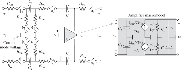
Switch Macromodel
As illustrated in Figure 4.2, switches are usually modeled as a linear switch on-resistance ![]() in series with an ideal switch, which is controlled by the corresponding clock phase, either
in series with an ideal switch, which is controlled by the corresponding clock phase, either ![]() or
or ![]() . Note that the switch model in SPICE-like simulators consists of a highly nonlinear resistor whose resistance depends on the control clock-phase voltage
. Note that the switch model in SPICE-like simulators consists of a highly nonlinear resistor whose resistance depends on the control clock-phase voltage ![]() as follows:
as follows:
4.1 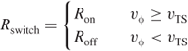
where ![]() stands for the switch off-resistance that is ideally
stands for the switch off-resistance that is ideally ![]() , and
, and ![]() stands for a threshold voltage that determines if the switch is either closed (on) or open (off). In practice, an almost ideal switch can be modeled in electrical simulators by setting
stands for a threshold voltage that determines if the switch is either closed (on) or open (off). In practice, an almost ideal switch can be modeled in electrical simulators by setting ![]() and
and ![]() just high/low enough to be negligible with respect to other circuit elements [3]. For instance, typical values of
just high/low enough to be negligible with respect to other circuit elements [3]. For instance, typical values of ![]() are chosen to be in the order of
are chosen to be in the order of ![]() , while a very high value of
, while a very high value of ![]() is considered, typically in the order of
is considered, typically in the order of ![]() .1
.1
Instead of using this simple model, a macromodel that is closer to the transistor-level topology implementation can be used. For instance, let us consider a CMOS switch similar to those shown in the sampling circuit of Figure 2.21. This switch is made up of a pMOS switch and an nMOS switch connected in parallel. Figure 4.4 shows an equivalent circuit that takes into account the on-resistance of both MOST switches as well as their associated parasitic capacitances, denoted as ![]() . Note that this macromodel keeps the symmetry of the original MOST-based circuit.
. Note that this macromodel keeps the symmetry of the original MOST-based circuit.
Figure 4.4 Macromodel of a CMOS switch.

OTA Macromodel
The OTA circuit is modeled by a well-known single-pole amplifier where ![]() ,
, ![]() , and
, and ![]() denote, respectively, the transconductance, output conductance, and output capacitance. In addition, the voltage-controlled current source used for modeling the OTA transconductance has two saturation limits,
denote, respectively, the transconductance, output conductance, and output capacitance. In addition, the voltage-controlled current source used for modeling the OTA transconductance has two saturation limits, ![]() . These limits model the minimum and maximum output currents provided by the OTA. This way, this equivalent circuit takes into account the finite DC gain, GB, and SR limitations of the OTA, respectively given by
. These limits model the minimum and maximum output currents provided by the OTA. This way, this equivalent circuit takes into account the finite DC gain, GB, and SR limitations of the OTA, respectively given by
4.2 ![]()
Note that real values of GB and SR deviate in practice from the above expressions because of the effect caused by bottom-plate parasitic capacitances, denoted as ![]() in Figure 4.3, as well as the capacitive load due to the SC network connected at the output of the integrator.
in Figure 4.3, as well as the capacitive load due to the SC network connected at the output of the integrator.
4.1.2 CT Integrator Macromodel
The equivalent circuit normally used for the macromodel of CT integrators is based on a one-pole (or two-pole) OTA model together with the additional circuit elements that are required to implement the integrator topology, that is, Gm-C, active-RC, etc. [5].
Active-RC Integrators
Figure 4.5 shows a simple macromodel circuit commonly used for active-RC implementations. In this example, a one-pole OTA model similar to that shown in Figures 4.2 and 4.3 is used, although higher dynamics can be implemented if necessary. In a similar way to SC integrators, parasitic and load capacitances of the OTA can also be considered.
Figure 4.5 Active-RC integrator macromodel: (a) single-ended schematic and (b) fully-differential schematic.

Gm-C Integrators
On the basis of the same OTA macromodel circuit, Gm-C integrators can be modeled by the equivalent circuit shown in Figure 4.6a, which includes a second pole modeled by the time constant ![]() . In this case, the
. In this case, the ![]() -domain transfer function of the integrator is given by
-domain transfer function of the integrator is given by
4.3 ![]()
Figure 4.6 Gm-C integrator macromodel: (a) two-pole linear model and (b) one-pole weakly nonlinear model.
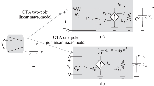
4.1.3 Nonlinear OTA Transconductor
The OTA macromodel considered in previous sections assumed a linear model for the transconductance ![]() and an output current saturation
and an output current saturation ![]() . In practice, the transconductor of the OTA is assumed to be weakly nonlinear, such that its static output current
. In practice, the transconductor of the OTA is assumed to be weakly nonlinear, such that its static output current ![]() is related to the OTA input voltage
is related to the OTA input voltage ![]() as follows [6]:
as follows [6]:

where ![]() denotes the sign function of
denotes the sign function of ![]() ,
, ![]() is the third-order nonlinear coefficient of the transconductor, IIP3 stands for the input-referred third-order intercept point, and
is the third-order nonlinear coefficient of the transconductor, IIP3 stands for the input-referred third-order intercept point, and ![]() is the maximum output current provided by the transconductor. It can be shown from Equation 4.4 that IIP3 and
is the maximum output current provided by the transconductor. It can be shown from Equation 4.4 that IIP3 and ![]() are related to
are related to ![]() and
and ![]() as follows:
as follows:
4.5 ![]()
4.6 ![]()
Figure 4.6b shows an equivalent circuit for the OTA macromodel that includes the weakly nonlinear transconductance element. Note that this equivalent circuit can be easily modeled in SPICE-like simulators using nonlinear voltage-controlled current sources [3]. Moreover, other sources of nonlinearities associated with the voltage dependency of integrated resistors and capacitors can also be included in the integrator macromodels using signal-dependent voltage/current sources. However, this kind of nonlinear effects are more accurately considered in the simulation when the circuit is modeled at device level, that is, taking into account the device models provided by the foundry, such as unsalicided polysilicon resistors or MiM capacitors.
4.1.4 Embedded Flash ADC Macromodel
Multibit/multilevel ADCs required to implement the quantizers embedded in ![]() Ms are typically implemented using a well-known flash architecture. This kind of ADCs is made up of a bank of comparators that compare the quantizer input signal (i.e., the output of the integrator connected to the quantizer) with a set of reference voltages generated in a resistor ladder [7]. These reference voltages correspond to the transition points between the different adjacent quantization intervals [8].
Ms are typically implemented using a well-known flash architecture. This kind of ADCs is made up of a bank of comparators that compare the quantizer input signal (i.e., the output of the integrator connected to the quantizer) with a set of reference voltages generated in a resistor ladder [7]. These reference voltages correspond to the transition points between the different adjacent quantization intervals [8].
As an illustration, Figure 4.7a shows the fully-differential schematic of a trilevel flash ADC, which is made up of two comparators and a resistive divider. The latter is made up of four unit resistors ![]() , which are connected in series between the negative reference voltage
, which are connected in series between the negative reference voltage ![]() and the positive reference voltage
and the positive reference voltage ![]() . In this example, there are two transition points,
. In this example, there are two transition points, ![]() and
and ![]() , in the quantizer differential characteristic illustrated in Figure 4.7b, which correspond to the differential tabs of the resistor ladder in Figure 4.7a. Thus, the quantizer input
, in the quantizer differential characteristic illustrated in Figure 4.7b, which correspond to the differential tabs of the resistor ladder in Figure 4.7a. Thus, the quantizer input ![]() is compared with
is compared with ![]() and
and ![]() , in the first and the second comparator, respectively. The thermometer code generated at the comparators outputs is converted into a 1-of-3 code (
, in the first and the second comparator, respectively. The thermometer code generated at the comparators outputs is converted into a 1-of-3 code (![]() ) using three AND gates.
) using three AND gates.
Figure 4.7 Macromodeling multilevel flash ADCs: (a) conceptual schematic of a trilevel flash ADC and (b) static differential transfer characteristic.

Figure 4.8 Verilog-A code used for simulating comparators in quantizer macromodels [10, 11].

The circuit shown in Figure 4.7a can be used for simulating ![]() Ms with macromodels. To this end, resistors are considered ideal circuit elements,2 while comparators and AND gates are modeled using Verilog-A. As an illustration, Figure 4.8 shows the Verilog-A code used for modeling the comparators in Figure 4.7. The model—based on the Open Verilog International (OVI) language reference manual [10, 11]—is quite simple and includes the input offset. The comparison only takes place when the clock signal named enable is in the high state. The static input–output transfer characteristic is computed by using an hyperbolic tangent function (tanh), which is scaled by a parameter named comp_slope. The latter determines the static resolution of the comparator by modifying the voltage gain around the input offset voltage, modeled by sigin_offset parameter.
Ms with macromodels. To this end, resistors are considered ideal circuit elements,2 while comparators and AND gates are modeled using Verilog-A. As an illustration, Figure 4.8 shows the Verilog-A code used for modeling the comparators in Figure 4.7. The model—based on the Open Verilog International (OVI) language reference manual [10, 11]—is quite simple and includes the input offset. The comparison only takes place when the clock signal named enable is in the high state. The static input–output transfer characteristic is computed by using an hyperbolic tangent function (tanh), which is scaled by a parameter named comp_slope. The latter determines the static resolution of the comparator by modifying the voltage gain around the input offset voltage, modeled by sigin_offset parameter.
4.1.5 Feedback DAC Macromodel
There are essentially two types of feedback DAC circuits used in ![]() Ms, namely SC DACs and current mode, also named current-steering (CS) DACs [12]. The former are mainly used in SC-
Ms, namely SC DACs and current mode, also named current-steering (CS) DACs [12]. The former are mainly used in SC-![]() Ms, although they are used also in some CT-
Ms, although they are used also in some CT-![]() Ms, specifically those implemented with active-RC integrators intended for low-frequency applications [13]. In contrast, switched-current3 or current-steering feedback DACs are commonly used in wideband CT-
Ms, specifically those implemented with active-RC integrators intended for low-frequency applications [13]. In contrast, switched-current3 or current-steering feedback DACs are commonly used in wideband CT-![]() Ms, particularly—but not only—those based on Gm-C loop-filter implementations.
Ms, particularly—but not only—those based on Gm-C loop-filter implementations.
As an example of SC DACs, let us consider again the trilevel ADC shown in Figure 4.7a. The 1-of-3 coded digital output ![]() is fed back to the
is fed back to the ![]() M loop-filter SC integrators by using three AND gates as illustrated in Figure 4.9. In this case, the macromodel of the DAC is simply based on the Verilog-A models of the AND gates as well as the macromodel circuits used for the switches described in Section 4.1.1.
M loop-filter SC integrators by using three AND gates as illustrated in Figure 4.9. In this case, the macromodel of the DAC is simply based on the Verilog-A models of the AND gates as well as the macromodel circuits used for the switches described in Section 4.1.1.
Figure 4.9 Macromodel of a trilevel SC DAC connected to an SC FE integrator within a ![]() M loop filter. Note that different SC branches, using two different sampling capacitors
M loop filter. Note that different SC branches, using two different sampling capacitors ![]() and
and ![]() , are used in this model. However, there are many situations in practice where a single SC branch is shared by both the input signal and the feedback DAC as will be shown later in this chapter.
, are used in this model. However, there are many situations in practice where a single SC branch is shared by both the input signal and the feedback DAC as will be shown later in this chapter.

Figure 4.10 Illustrating the macromodel of a trilevel current-steering DAC connected to a Gm-C integrator within a ![]() M loop filter.
M loop filter.

Following the same philosophy, a macromodel circuit that can be used for current-steering DACs is based on simple macromodels of current sources and switches.4 As an illustration, Figure 4.10 shows the macromodel of a fully-differential trilevel current-steering NRZ DAC. It consists of a set of current sources controlled, through switches, by a 1-of-3 coded digital data (![]() ). As will be discussed later in this chapter, the ideal operation of the current sources, and consequently the current-steering DAC, is degraded in practice by mismatch errors, finite output impedance (of the current sources), thermal gradients, etc. The majority of these errors, such as mismatch and technology-related errors, require doing a large number of simulations in order to evaluate their impact on the performance of the modulator. For that reason, these errors are usually considered at system-level behavioral models, for instance implemented in MATLAB/SIMULINK as described in Chapter 3. Some other nonidealities, such as output impedance of current sources, which also affect the dynamic operation of the modulator loop filter, can be easily macromodeled by simply including an output resistance in parallel with each unit (or reference) current source, as illustrated in Figure 4.10.
). As will be discussed later in this chapter, the ideal operation of the current sources, and consequently the current-steering DAC, is degraded in practice by mismatch errors, finite output impedance (of the current sources), thermal gradients, etc. The majority of these errors, such as mismatch and technology-related errors, require doing a large number of simulations in order to evaluate their impact on the performance of the modulator. For that reason, these errors are usually considered at system-level behavioral models, for instance implemented in MATLAB/SIMULINK as described in Chapter 3. Some other nonidealities, such as output impedance of current sources, which also affect the dynamic operation of the modulator loop filter, can be easily macromodeled by simply including an output resistance in parallel with each unit (or reference) current source, as illustrated in Figure 4.10.
4.1.6 Examples of  M Macromodels
To conclude this section, a couple of examples are described to illustrate the use of the macromodels for the implementation of ![]() Ms. The first one is based on SC circuits while the second one is implemented with active-RC circuits. In both cases, the well-known, single-loop, second-order
Ms. The first one is based on SC circuits while the second one is implemented with active-RC circuits. In both cases, the well-known, single-loop, second-order ![]() M is used as a demonstration vehicle, considering an embedded trilevel quantizer.
M is used as a demonstration vehicle, considering an embedded trilevel quantizer.
SC Second-Order Example
Figure 4.11 shows the conceptual schematic of the second-order SC-![]() M under study, which includes a trilevel embedded quantizer. The values of capacitors used are highlighted in the figure. The circuit elements forming this modulator—that is switches, amplifiers, a flash (trilevel) ADC, and an SC (trilevel) DAC—can be implemented using the macromodels described in previous section.
M under study, which includes a trilevel embedded quantizer. The values of capacitors used are highlighted in the figure. The circuit elements forming this modulator—that is switches, amplifiers, a flash (trilevel) ADC, and an SC (trilevel) DAC—can be implemented using the macromodels described in previous section.
Figure 4.11 Conceptual schematic of a second-order SC-![]() M with a trilevel embedded quantizer.
M with a trilevel embedded quantizer.

Figure 4.12 shows the schematic of the modulator in Figure 4.11 implemented in Cadence Design FrameWork, using Cadence Virtuoso Schematic. In this example, ideal clock phases (implemented with ideal voltage sources) are used for the sake of simplicity. This is a common practice at the very beginning of the design phase as the use of a clock-phase generator circuit—discussed later in this chapter—slows down the simulations unnecessarily.
Figure 4.12 Implementation of the modulator in Figure 4.11 using Cadence Virtuoso Schematics.

Note that each modulator building block in Figure 4.12 uses a suitable schematic symbol. This is very useful in practice to clearly identify the different parts of the modulator and to establish an appropriate hierarchic partitioning that allows us to systematize the design from a top-down/bottom-up approach. This way, designers can move through the modulator hierarchy, using the most convenient schematic representation according to the circuit part being analyzed. As an illustration, Figure 4.13 shows the macromodel of the first integrator in Figure 4.12, where the symbols for the switches, capacitors, and opamps are clearly identified.
Figure 4.13 Schematic of the SC first integrator of Figure 4.12.

As discussed earlier in this chapter, the use of even ideal macromodels allows designers to clearly define the electrical representation of a ![]() M circuit, including all their nodes and branches. These macromodels can be progressively replaced by their transistor-level implementations as the different building blocks are being sized. This is something that can be done very easily in some circuit design environments, such as in Cadence Design Framework. Figure 4.14 shows how to change the type of implementation, often referred to as view. Note that four different cell view names are available in this example: symbol (which is the highest abstraction level), macromodel, schematic (transistor-level), and layout.
M circuit, including all their nodes and branches. These macromodels can be progressively replaced by their transistor-level implementations as the different building blocks are being sized. This is something that can be done very easily in some circuit design environments, such as in Cadence Design Framework. Figure 4.14 shows how to change the type of implementation, often referred to as view. Note that four different cell view names are available in this example: symbol (which is the highest abstraction level), macromodel, schematic (transistor-level), and layout.
Figure 4.14 Illustrating the selection of a circuit view name in Cadence Design FrameWork.

As an illustration, Figure 4.15 shows the macromodel of different parts of the SC integrator in Figure 4.13. Figure 4.15a shows the macromodel of the fully-differential amplifier and Figure 4.15b depicts the macromodel of a CMOS switch. In both cases, the different model parameters can be set according to the building-block specifications derived from behavioral simulations, for instance using SIMSIDES as described in Chapter 3.
Figure 4.15 Illustrating the macromodel implementation of different circuit elements of SC integrators in Cadence Design FrameWork: (a) fully-differential amplifier and (b) switch.

Second-Order Active-RC  M
M
Figure 4.16 shows the conceptual schematic of a second-order active-RC ![]() M with trilevel embedded quantizer. For the sake of simplicity, the modulator does not include any excess-loop delay cancellation technique. The values and expressions of the resistances, capacitances, and feedback DAC currents are shown in the figure, where
M with trilevel embedded quantizer. For the sake of simplicity, the modulator does not include any excess-loop delay cancellation technique. The values and expressions of the resistances, capacitances, and feedback DAC currents are shown in the figure, where ![]() denotes the FS reference voltage of the modulator.
denotes the FS reference voltage of the modulator.
Figure 4.16 Conceptual schematic of a second-order active-RC ![]() M with a trilevel embedded quantizer and CS feedback DACs.
M with a trilevel embedded quantizer and CS feedback DACs.

The circuit shown in Figure 4.16 can be modeled very easily using the macromodel circuits described in previous sections. Figure 4.17 shows an example implemented in Cadence Virtuoso schematic editor, highlighting the main parts of the circuit. The opamp included in the active-RC model (Figure 4.17b) uses the macromodel described in Figure 4.5b. In this example, the trilevel quantization is implemented as illustrated in Figure 4.18. The ADC, depicted in Figure 4.18a, is modeled as shown in Figure 4.7b. However, for the sake of simplicity, the current-steering DAC, shown in Figure 4.18b, is modeled by two ideal voltage-controlled current sources, which emulate the ideal switches connected in series with the reference currents (Figure 4.10).
Figure 4.17 Schematic of the modulator in Figure 4.16 implemented in Cadence Virtuoso schematic editor: (a) modulator and (b) active-RC integrator.

Figure 4.18 Illustrating the macromodel implementation of a trilevel quantizer in Cadence Virtuoso schematic editor: (a) flash ADC and (b) current-steering DAC.

4.2 Including Noise in Transient Electrical Simulations of  Ms
Ms
As stated in Chapter 2, circuit noise is an ultimate limiting factor degrading the performance of ![]() Ms. Therefore, it is essential to take into account this effect in all steps of the design flow. At system level, accurate models described in Chapter 2 can be incorporated in behavioral simulations, for instance, using SIMSIDES as detailed in Chapter 3. At electrical level, however, the majority of SPICE-like simulators do not include noise sources in the transient analysis,5 which makes their analysis at transistor level more complicated.
Ms. Therefore, it is essential to take into account this effect in all steps of the design flow. At system level, accurate models described in Chapter 2 can be incorporated in behavioral simulations, for instance, using SIMSIDES as detailed in Chapter 3. At electrical level, however, the majority of SPICE-like simulators do not include noise sources in the transient analysis,5 which makes their analysis at transistor level more complicated.
This section describes a methodology that allows designers to do electrical (transistor-level) simulations of ![]() Ms including noise sources. The method—based on generating a noisy data sequence in MATLAB and then injecting this data sequence in the electrical simulation—can be used in most SPICE-like simulators such as PSPICE and HSPICE [4, 16].
Ms including noise sources. The method—based on generating a noisy data sequence in MATLAB and then injecting this data sequence in the electrical simulation—can be used in most SPICE-like simulators such as PSPICE and HSPICE [4, 16].
4.2.1 Generating and Injecting Noise Data Sequences in HSPICE
Let us consider the simple SC circuit shown in Figure 4.19a, in which a noise voltage source ![]() is sampled by an ideal switch
is sampled by an ideal switch ![]() and stored on capacitor
and stored on capacitor ![]() . This circuit can be simulated using the HSPICE netlist shown in Figure 4.19b. In this example
. This circuit can be simulated using the HSPICE netlist shown in Figure 4.19b. In this example ![]() pF, the switch off/on-resistances used in the ideal switch model are, respectively,
pF, the switch off/on-resistances used in the ideal switch model are, respectively, ![]() and
and ![]() and the clock frequency is
and the clock frequency is ![]() MHz. Note that the noise sequence data is
MHz. Note that the noise sequence data is ![]() in the HSPICE transient simulation through the use of the .DATA statement [16]. This command allows inclusion of data that has been externally generated. In this example, a two-column (time, voltage) format file, named noisedata, is loaded, and the transient analysis uses the time data provided in column 1 of file noisedata as the sweep input parameter.
in the HSPICE transient simulation through the use of the .DATA statement [16]. This command allows inclusion of data that has been externally generated. In this example, a two-column (time, voltage) format file, named noisedata, is loaded, and the transient analysis uses the time data provided in column 1 of file noisedata as the sweep input parameter.
Figure 4.19 Injecting noise data sequences in transient HSPICE simulations: (a) sampling circuit example and (b) SPICE netlist.

In order to compute the noise data used in the electrical simulations, it should be taken into account that ![]() is a random signal, and hence, its instantaneous value is not known. Instead, it can be described as a random process of zero mean and an amplitude uniformly distributed in the range
is a random signal, and hence, its instantaneous value is not known. Instead, it can be described as a random process of zero mean and an amplitude uniformly distributed in the range ![]() , where
, where ![]() denotes the rms value of
denotes the rms value of ![]() . In this case, the mean-square value of
. In this case, the mean-square value of ![]() is given by [17]
is given by [17]
4.7 
Assuming a band-limited noise source, the PSD of ![]() can be computed as
can be computed as
4.8 ![]()
where ![]() stands for the equivalent noise bandwidth of
stands for the equivalent noise bandwidth of ![]() . Hence, if
. Hence, if ![]() is sampled at
is sampled at ![]() , the value of
, the value of ![]() at instant
at instant ![]() can be computed as
can be computed as
where ![]() represents a random number in the range
represents a random number in the range ![]() and
and ![]() [18].
[18].
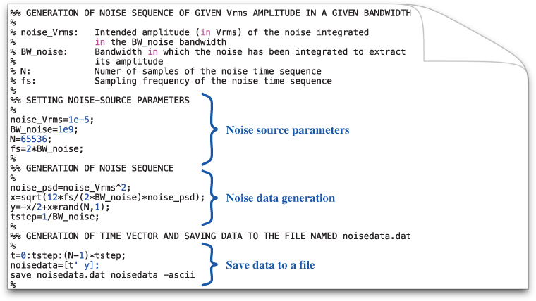
Figure 4.20 shows the MATLAB code used for generating an ![]() -point data sequence derived from Equation 4.9. Note that the data sequence is saved as a two-column format file, in which the first column represents the time series (i.e.,
-point data sequence derived from Equation 4.9. Note that the data sequence is saved as a two-column format file, in which the first column represents the time series (i.e., ![]() ) and the second column is the noise data sequence generated using Equation 4.9.
) and the second column is the noise data sequence generated using Equation 4.9.
Figure 4.20 MATLAB code used for generating an ![]() -point data sequence derived from Equation 4.9.
-point data sequence derived from Equation 4.9.
As an illustration, Figure 4.21 shows the PSD of the noise sampled and stored in the capacitor of Figure 4.19a, considering different values of ![]() . In this example, a noise source with
. In this example, a noise source with ![]() Vrms,
Vrms, ![]() GHz, and
GHz, and ![]() was considered in order to emulate an unlimited-band noise source. This way, the time interval between two consecutive samples is low enough (1 ns in this example), thus enabling to model the noise source as a CT source [19], which is filtered by the circuit made up of
was considered in order to emulate an unlimited-band noise source. This way, the time interval between two consecutive samples is low enough (1 ns in this example), thus enabling to model the noise source as a CT source [19], which is filtered by the circuit made up of ![]() and
and ![]() , with
, with ![]() being the switch on-resistance. This results in an equivalent bandwidth of the sampled noise given by
being the switch on-resistance. This results in an equivalent bandwidth of the sampled noise given by ![]() . As shown in Figure 4.21, aliasing occurs in this case because
. As shown in Figure 4.21, aliasing occurs in this case because ![]() . As a consequence the noise power increases within the Nyquist band, that is, from DC to
. As a consequence the noise power increases within the Nyquist band, that is, from DC to ![]() .
.
Figure 4.21 Illustrating the effect of sampling noise in HSPICE transient simulations. Output spectrum of the voltage stored in ![]() in Figure 4.19a, considering the following simulation data:
in Figure 4.19a, considering the following simulation data: ![]() ,
, ![]() pF,
pF, ![]() 1 MHz.
1 MHz.

4.2.2 Analyzing the Impact of Main Noise Sources in SC Integrators
The simulation technique formerly described can be used for verifying the impact of most critical noise sources on the performance of main ![]() building blocks through transient SPICE simulations. This is particularly critical in SC circuits because of the action of their sampled-data circuit nature, with the subsequent effect of the sampling process on noise sources.
building blocks through transient SPICE simulations. This is particularly critical in SC circuits because of the action of their sampled-data circuit nature, with the subsequent effect of the sampling process on noise sources.
As an illustration, let us consider an SC FE integrator similar to that shown in Figure 3.5a. As stated in Chapter 2, their main sources of circuit noise are generated in the switches and in the amplifier. Figure 4.22 shows the circuit schematics that can be used for evaluating the influence of these noise sources on SC integrators and Figure 4.23 shows the corresponding HSPICE netlist. Note that all circuits are built through simple macromodels for the switches and the amplifier in order to isolate the effect of the different error sources to be considered. Figure 4.22a shows the schematic used for simulating the thermal noise introduced by switches controlled by clock phase ![]() , and Figure 4.22b shows the corresponding test-bench schematic for the evaluation of thermal noise generated in the switches controlled by
, and Figure 4.22b shows the corresponding test-bench schematic for the evaluation of thermal noise generated in the switches controlled by ![]() . The test-bench schematic used for the noise sources generated in the amplifier is shown in Figure 4.22c. In the latter case, both thermal and flicker noise components need to be generated. This can be done as detailed in the next section.
. The test-bench schematic used for the noise sources generated in the amplifier is shown in Figure 4.22c. In the latter case, both thermal and flicker noise components need to be generated. This can be done as detailed in the next section.
Figure 4.22 Equivalent single-ended circuits used for simulating the effect of main noise sources in SC integrators: (a) noise contribution of switches controlled by ![]() and (b) noise contribution of switches controlled by
and (b) noise contribution of switches controlled by ![]() , and (c) noise contribution of the amplifier.
, and (c) noise contribution of the amplifier.

Figure 4.23 HSPICE netlist of the circuits shown in Figure 4.22.

4.2.3 Generating and Injecting Flicker Noise Sources in Electrical Simulations
The procedure described in Section 4.2.1 assumed white noise sources. However, some noise sources of noise in ![]() Ms also include flicker (
Ms also include flicker (![]() ) noise components that might be critical in low-bandwidth applications such as sensors, instrumentation, and biomedical applications.
) noise components that might be critical in low-bandwidth applications such as sensors, instrumentation, and biomedical applications.
Flicker noise can be generated as a colored noise sequence in MATLAB by filtering a white noise source through a filter with the following transfer function [20]
4.10 ![]()
where ![]() is a real number between 0 and 2. This way, the corresponding noise sequence data can be injected in HSPICE transient simulations using the same method as that described in previous sections.
is a real number between 0 and 2. This way, the corresponding noise sequence data can be injected in HSPICE transient simulations using the same method as that described in previous sections.
Alternatively, colored noise data sequence, including both ![]() and white noise components, can be generated by extracting the PSD data of the corresponding noise source using a .NOISE analysis in SPICE and then, generating a noise time sequence in MATLAB which is equivalent to the captured PSD, and that can be injected in transient simulations using the .DATA statement.
and white noise components, can be generated by extracting the PSD data of the corresponding noise source using a .NOISE analysis in SPICE and then, generating a noise time sequence in MATLAB which is equivalent to the captured PSD, and that can be injected in transient simulations using the .DATA statement.
Figure 4.24 shows a MATLAB code used for generating a time data sequence according to the electrical data captured from a .NOISE simulation in HSPICE. In this example, simulation output data resulting from the noise analysis in HSPICE is stored in a file named psd_eq_preamp_1f_white_RRF.dat, which is assumed to be expressed in ![]() Hz, that is, corresponding to a PSD curve. Both PSD and rms values of the
Hz, that is, corresponding to a PSD curve. Both PSD and rms values of the ![]() and white noise components are identified and computed, and the corresponding time data series are generated using Equation 4.9.
and white noise components are identified and computed, and the corresponding time data series are generated using Equation 4.9.
Figure 4.24 MATLAB code used for generating colored noise data sequence extracted from HSPICE .NOISE simulation.

As an illustration, Figure 4.25 shows the output spectra generated by the MATLAB routine in Figure 4.24. Note that a huge number of points (![]() in this example) are required to generate FFTs at low frequencies and see the flicker noise corner frequency.
in this example) are required to generate FFTs at low frequencies and see the flicker noise corner frequency.
Figure 4.25 Output spectrum generated by the MATLAB routine shown in Figure 4.24.

4.2.4 Test Bench to Include Noise in the Simulation of  Ms
Ms
At the end of the design phase, transistor-level simulations of the whole ![]() M are mandatory in order to check that the electrical performance agrees with system-level behavioral simulations, and consequently with target specifications. In this situation, injecting noise sources in SPICE transient simulations is required. To this end, the total input-referred noise source, including the effect of sampling, can be generated and injected at the input node of the modulator following the methodology described in previous sections.
M are mandatory in order to check that the electrical performance agrees with system-level behavioral simulations, and consequently with target specifications. In this situation, injecting noise sources in SPICE transient simulations is required. To this end, the total input-referred noise source, including the effect of sampling, can be generated and injected at the input node of the modulator following the methodology described in previous sections.
As an illustration, Figure 4.26a shows how to inject noise in transient simulations carried out using Cadence Virtuoso Schematic Editor [21] and Cadence-Spectre simulator [15]. The input-referred noise source is injected in the modulator (a fourth-order cascade 2-2 SC architecture in this example) by including a piece-wise linear (PWL) voltage source at the input node. The noise data sequence is loaded from a file as shown in Figure 4.26b. In this case, the noise data sequence is generated using the MATLAB code shown in Figure 4.27, where the standard deviation of the noise source is computed as
where ![]() is the sampling frequency of the modulator,
is the sampling frequency of the modulator, ![]() is the signal bandwidth, and
is the signal bandwidth, and ![]() (power_IBN in Figure 4.27) is the IBN due to the noise source—derived from the behavioral simulation data provided by SIMSIDES. Note that in this example, a Gaussian noise is generated using the randn function provided by MATLAB. Several cases of IBN are considered, which correspond to a reconfigurable
(power_IBN in Figure 4.27) is the IBN due to the noise source—derived from the behavioral simulation data provided by SIMSIDES. Note that in this example, a Gaussian noise is generated using the randn function provided by MATLAB. Several cases of IBN are considered, which correspond to a reconfigurable ![]() M for multistandard applications. As an illustration, Figure 4.28 shows the output spectrum of a fourth-order cascade 2-2 SC-
M for multistandard applications. As an illustration, Figure 4.28 shows the output spectrum of a fourth-order cascade 2-2 SC-![]() M, in which the effect of injecting thermal noise is highlighted. In this example, macromodels have been considered in all
M, in which the effect of injecting thermal noise is highlighted. In this example, macromodels have been considered in all ![]() building blocks in order to speed up the simulation, although the method is obviously valid for transistor-level simulations as well.
building blocks in order to speed up the simulation, although the method is obviously valid for transistor-level simulations as well.
Figure 4.26 Test-bench example to inject noise in transient simulations of ![]() Ms using Cadence-Spectre simulator: (a) schematic in the Virtuoso editor environment and (b) object properties windows highlighting how to load the noise data sequence file.
Ms using Cadence-Spectre simulator: (a) schematic in the Virtuoso editor environment and (b) object properties windows highlighting how to load the noise data sequence file.

Figure 4.27 MATLAB code used for generating an ![]() -point data sequence derived from Equation 4.11.
-point data sequence derived from Equation 4.11.

Figure 4.28 Output spectrum of a fourth-order cascade 2-2 SC-![]() M. The simulation was carried out in Cadence-Spectre, considering macromodels for all building blocks and injecting the input-referred noise source as illustrated in Figure 4.26.
M. The simulation was carried out in Cadence-Spectre, considering macromodels for all building blocks and injecting the input-referred noise source as illustrated in Figure 4.26.

4.3 Processing  M Output Results of Electrical Simulations
The ![]() M output bitstreams obtained by electrical simulations need to be properly processed in order to characterize main figures of merit, namely output spectrum, IBN, SNR/SNDR, THD, etc. To this purpose, the following step-by-step procedure can be followed:6
M output bitstreams obtained by electrical simulations need to be properly processed in order to characterize main figures of merit, namely output spectrum, IBN, SNR/SNDR, THD, etc. To this purpose, the following step-by-step procedure can be followed:6
Figure 4.29 shows a conceptual diagram of the step-by-step procedure formerly described, considering that the electrical simulations are carried out with Cadence-Spectre, and the results are processed using SIMSIDES. As an example, let us consider a fourth-order cascade 2-2 SC-![]() M with trilevel quantization in both stages. Figure 4.30a shows the test-bench schematic used in Cadence to simulate the modulator. In this example, the output of the front-end and the back-end stages of the modulator are, respectively, named Output1<1:3> and Output2<1:3>, where Outputj<i> corresponds to the
M with trilevel quantization in both stages. Figure 4.30a shows the test-bench schematic used in Cadence to simulate the modulator. In this example, the output of the front-end and the back-end stages of the modulator are, respectively, named Output1<1:3> and Output2<1:3>, where Outputj<i> corresponds to the ![]() th output bit of the
th output bit of the ![]() th stage quantizer, considering a 1-of-3 digital code as illustrated in Figure 4.7. Overall, six bitstreams are collected and stored in a text file. This task is implemented by the blocks named WRITE OUTPUT, which implement the Verilog-A code shown in Figure 4.30b. Note that the output data—consisting of the three bitstreams named Out1, Out2, Out3—are collected and stored in the text file at a rate of one sample per clock cycle as illustrated in Figure 4.30c. The event at which the data are collected is governed by a trigger signal, named trigger in this example. This trigger signal corresponds to the clock phase in which the comparator outputs are settled, which in this example is clock phase
th stage quantizer, considering a 1-of-3 digital code as illustrated in Figure 4.7. Overall, six bitstreams are collected and stored in a text file. This task is implemented by the blocks named WRITE OUTPUT, which implement the Verilog-A code shown in Figure 4.30b. Note that the output data—consisting of the three bitstreams named Out1, Out2, Out3—are collected and stored in the text file at a rate of one sample per clock cycle as illustrated in Figure 4.30c. The event at which the data are collected is governed by a trigger signal, named trigger in this example. This trigger signal corresponds to the clock phase in which the comparator outputs are settled, which in this example is clock phase ![]() .
.
Figure 4.29 Step-by-step procedure to process electrical simulation outputs.

Figure 4.30 Collecting and storing the output bitstreams of a ![]() M in an electrical simulation: (a) test-bench schematic in Cadence Design FrameWork, (b) Verilog-A code to capture simulation output results, and (c) excerpt of the generated output file (text format).
M in an electrical simulation: (a) test-bench schematic in Cadence Design FrameWork, (b) Verilog-A code to capture simulation output results, and (c) excerpt of the generated output file (text format).

Once the simulation output data has been stored in a multicolumn text file, this data can be loaded and processed using the MATLAB routine shown in Figure 4.31a. Note that the bitstreams of both stages are scaled from the values of the supply voltage (1.2V) to 1V and the 1-of-3 codification is transformed into a single-bit output format. Both output bitstreams are processed by a DCL implemented in SIMULINK as shown in Figure 4.31b. Once this DCL diagram is simulated, the overall modulator output is saved into the MATLAB workspace and can be processed using SIMSIDES post-processing facilities. As an illustration, the output spectrum shown in Figure 4.28 was obtained using the procedure and routines described in this section.
Figure 4.31 MATLAB routine used for processing ![]() M outputs from electrical simulations: (a) MATLAB code and (b) DCL block diagram implemented in SIMULINK.
M outputs from electrical simulations: (a) MATLAB code and (b) DCL block diagram implemented in SIMULINK.
4.4 Design Considerations and Simulation Test Benches of  M Basic Building Blocks
Once the modulator has been verified using macromodels and the performance has been evaluated considering main nonideal circuit and physical effects (including circuit noise), the next step is the electrical transistor-level design of ![]() M building blocks and circuit elements. In this book, we will distinguish between two different categories of
M building blocks and circuit elements. In this book, we will distinguish between two different categories of ![]() M building blocks or subcircuits. The first category, referred to as basic building blocks, includes the loop filter (essentially based on integrators and resonators) and the embedded quantizer, made up of an ADC (usually a flash ADC made of a bank of comparators) and a DAC. The second category includes a number of so-called auxiliary building blocks which are also needed to implement a
M building blocks or subcircuits. The first category, referred to as basic building blocks, includes the loop filter (essentially based on integrators and resonators) and the embedded quantizer, made up of an ADC (usually a flash ADC made of a bank of comparators) and a DAC. The second category includes a number of so-called auxiliary building blocks which are also needed to implement a ![]() M IC. Among others, the most important auxiliary blocks are the clock-phase generator, the master bias generator, the reference voltage generator, and the digital circuits required for buffering and signal processing.
M IC. Among others, the most important auxiliary blocks are the clock-phase generator, the master bias generator, the reference voltage generator, and the digital circuits required for buffering and signal processing.
This section deals with the design of basic ![]() M building blocks, focusing on their essential circuit elements, namely switches, comparators, OTAs, and DACs. The main design considerations concerning these circuits are described together with practical simulation test benches frequently used for characterizing their main electrical performance metrics, which have been derived from system-level behavioral simulations.
M building blocks, focusing on their essential circuit elements, namely switches, comparators, OTAs, and DACs. The main design considerations concerning these circuits are described together with practical simulation test benches frequently used for characterizing their main electrical performance metrics, which have been derived from system-level behavioral simulations.
4.4.1 Design Considerations of CMOS Switches
Practically, all switches used in SC-![]() Ms are of CMOS type, that is, based on a pMOS and an nMOS transistor connected in parallel, as illustrated in Figure 4.32.7 As stated in Chapters 2 and 3, the most important design specification of CMOS switches is the switch on-resistance
Ms are of CMOS type, that is, based on a pMOS and an nMOS transistor connected in parallel, as illustrated in Figure 4.32.7 As stated in Chapters 2 and 3, the most important design specification of CMOS switches is the switch on-resistance ![]() . The value of
. The value of ![]() is mainly constricted by dynamic considerations that affect the integrator transient response and consequently the effective resolution of the modulator [22].
is mainly constricted by dynamic considerations that affect the integrator transient response and consequently the effective resolution of the modulator [22].
Figure 4.32 Switch symbol and its equivalent CMOS circuit.

Let us consider that the CMOS switch of Figure 4.32 is switched on, that is, ![]() and
and ![]() . Assuming that the nMOS and pMOS transistors operate in the ohmic region, their on-resistances can be approximated by Equation 2.47, and the overall CMOS switch on-resistance is the result of the parallel connection of resistors
. Assuming that the nMOS and pMOS transistors operate in the ohmic region, their on-resistances can be approximated by Equation 2.47, and the overall CMOS switch on-resistance is the result of the parallel connection of resistors ![]() and
and ![]() .
.
Trade-Off Between  and the CMOS Switch Drain/Source Parasitic Capacitances
As discussed in Section 2.7.2, the value of ![]() can be reduced by increasing the aspect ratio (
can be reduced by increasing the aspect ratio (![]() ) of both transistors in the CMOS switch. However, this increases the transistors area, and consequently their associated drain/source parasitic capacitances, with the subsequent penalty in the transient response and integrators dynamics degradation. Therefore, there is a trade-off between the maximum value of
) of both transistors in the CMOS switch. However, this increases the transistors area, and consequently their associated drain/source parasitic capacitances, with the subsequent penalty in the transient response and integrators dynamics degradation. Therefore, there is a trade-off between the maximum value of ![]() that can be tolerated—which can be determined by behavioral simulation as shown in Chapter 3—and the drain/source parasitic capacitances associated with the CMOS switch that are in turn conditioned by the value of capacitors used in the SC branches. This way, switch transistor sizes can be scaled down across the modulator chain, using higher sizes in the front-end switches—where larger capacitors are chosen according to thermal noise considerations—while lower sizes are tolerated in back-end integrators, where smaller capacitors are normally used and hence the influence of switch parasitic capacitances is diminished.
that can be tolerated—which can be determined by behavioral simulation as shown in Chapter 3—and the drain/source parasitic capacitances associated with the CMOS switch that are in turn conditioned by the value of capacitors used in the SC branches. This way, switch transistor sizes can be scaled down across the modulator chain, using higher sizes in the front-end switches—where larger capacitors are chosen according to thermal noise considerations—while lower sizes are tolerated in back-end integrators, where smaller capacitors are normally used and hence the influence of switch parasitic capacitances is diminished.
Characterizing the Nonlinear Behavior of 
According to Equation 2.47, the values of ![]() and
and ![]() depend on the switch common-mode voltage,
depend on the switch common-mode voltage, ![]() , and hence on the drain and source voltages (denoted as
, and hence on the drain and source voltages (denoted as ![]() and
and ![]() in Figure 4.32) of the nMOS and pMOS transistors. As a consequence, the value of
in Figure 4.32) of the nMOS and pMOS transistors. As a consequence, the value of ![]() becomes a nonlinear function of the voltage being transmitted, thus generating harmonic distortion as discussed in Chapters 2 and 3.
becomes a nonlinear function of the voltage being transmitted, thus generating harmonic distortion as discussed in Chapters 2 and 3.
In order to evaluate the nonlinear characteristic of ![]() in CMOS switches, the circuit shown in Figure 4.33a can be used. The gate of nMOS transistor is connected to
in CMOS switches, the circuit shown in Figure 4.33a can be used. The gate of nMOS transistor is connected to ![]() and the gate of pMOS transistor is connected to
and the gate of pMOS transistor is connected to ![]() so that both transistors are switched on. A small voltage imbalance, typically in the order of 10–20 mV, is applied across the CMOS switch to guarantee that both nMOS and pMOS are properly biased and operate in the linear region. A DC common-mode voltage source is connected to the input node of the switch. This voltage is swept in a DC analysis in order to evaluate its impact on the variation of
so that both transistors are switched on. A small voltage imbalance, typically in the order of 10–20 mV, is applied across the CMOS switch to guarantee that both nMOS and pMOS are properly biased and operate in the linear region. A DC common-mode voltage source is connected to the input node of the switch. This voltage is swept in a DC analysis in order to evaluate its impact on the variation of ![]() .
.
Figure 4.33 Characterizing nonlinear switch on-resistance: (a) test-bench circuit, (b) HSPICE netlist, and (c) ![]() versus
versus ![]() considering a 90-nm CMOS technology with 1.2-V supply voltage.
considering a 90-nm CMOS technology with 1.2-V supply voltage.

Figure 4.33b shows the SPICE netlist used for simulating the circuit in Figure 4.33a. In this example, a 10-mV voltage, named vd, is applied across the switch and the common-mode voltage (vin in Figure 4.33a) is swept using a .DC analysis in SPICE. The value of ![]() can be extracted from each operating point in the .DC analysis by means of a parameter defined as PAR(1/(lx8(mp)+lx8(mn)) where lx8(mp,n) is an alias parameter used in HSPICE to represent the DC drain-source conductance of MOS transistors (
can be extracted from each operating point in the .DC analysis by means of a parameter defined as PAR(1/(lx8(mp)+lx8(mn)) where lx8(mp,n) is an alias parameter used in HSPICE to represent the DC drain-source conductance of MOS transistors (![]() and
and ![]() in Figure 4.33a). Thus, the values of
in Figure 4.33a). Thus, the values of ![]() and
and ![]() are extracted from 1/lx8(mn) and 1/lx8(mp), respectively [16].
are extracted from 1/lx8(mn) and 1/lx8(mp), respectively [16].
Figure 4.33c represents ![]() as a function of
as a function of ![]() , giving rise to a function similar to that shown in Figure 2.20b. The curves corresponding to both
, giving rise to a function similar to that shown in Figure 2.20b. The curves corresponding to both ![]() and
and ![]() are also depicted to illustrate the separate contribution of each transistor to the overall switch on-resistance. The maximum value of
are also depicted to illustrate the separate contribution of each transistor to the overall switch on-resistance. The maximum value of ![]() , denoted as ronmax, and the quiescent value of
, denoted as ronmax, and the quiescent value of ![]() , denoted as ronQ, can also be extracted from HSPICE simulations using the .meas command [16] as detailed in the netlist shown in Figure 4.33b.
, denoted as ronQ, can also be extracted from HSPICE simulations using the .meas command [16] as detailed in the netlist shown in Figure 4.33b.
The ![]() -versus-
-versus-![]() characteristic shown in Figure 4.33c has been obtained for
characteristic shown in Figure 4.33c has been obtained for ![]() , which according to Equation 2.47, gives an almost symmetrical function. An alternative approach consists of increasing
, which according to Equation 2.47, gives an almost symmetrical function. An alternative approach consists of increasing ![]() to equal
to equal ![]() , as illustrated in Figure 2.22. For the sake of completeness a similar figure is depicted in Figure 4.34, considering a 90-nm CMOS technology with a 1.2-V supply voltage. It can be noted how as
, as illustrated in Figure 2.22. For the sake of completeness a similar figure is depicted in Figure 4.34, considering a 90-nm CMOS technology with a 1.2-V supply voltage. It can be noted how as ![]() increases, the nonlinearity of the switch on-resistance increases, although its average value decreases. Hence, as discussed in Section 2.7.2, if the sizing of the nMOS and pMOS transistors in a CMOS switch compensates the difference in their transconductance parameters, the switch on-resistance nonlinearity is reduced, but the average on-resistance is larger than using the same sizes, that is,
increases, the nonlinearity of the switch on-resistance increases, although its average value decreases. Hence, as discussed in Section 2.7.2, if the sizing of the nMOS and pMOS transistors in a CMOS switch compensates the difference in their transconductance parameters, the switch on-resistance nonlinearity is reduced, but the average on-resistance is larger than using the same sizes, that is, ![]() . In the latter case, the area, and consequently the values of parasitic drain/source capacitances, increases as well although the overall effect of the finite switch on-resistance on the settling performance decreases [23]. Therefore, there is a design trade-off involving the switch on-resistance nonlinearity and its average value, which at the modulator level translates in the well-known analog design trade-off between speed (limited by the incomplete settling) and linearity (limited by nonlinear switch on-resistance) [22]. Nevertheless, in the majority of state-of-the-art SC-
. In the latter case, the area, and consequently the values of parasitic drain/source capacitances, increases as well although the overall effect of the finite switch on-resistance on the settling performance decreases [23]. Therefore, there is a design trade-off involving the switch on-resistance nonlinearity and its average value, which at the modulator level translates in the well-known analog design trade-off between speed (limited by the incomplete settling) and linearity (limited by nonlinear switch on-resistance) [22]. Nevertheless, in the majority of state-of-the-art SC-![]() Ms, CMOS switches are designed to keep a low enough average value of
Ms, CMOS switches are designed to keep a low enough average value of ![]() , while keeping a symmetrical
, while keeping a symmetrical ![]() -versus-
-versus-![]() characteristic similar to that shown in Figure 4.33c.
characteristic similar to that shown in Figure 4.33c.
Figure 4.34 ![]() versus
versus ![]() for different values of
for different values of ![]() , considering a 90-nm CMOS technology with 1.2-V supply voltage (
, considering a 90-nm CMOS technology with 1.2-V supply voltage (![]() nm).
nm).

Influence of Technology Downscaling
According to Equation 2.47, the reduction of the supply voltage caused by CMOS technology downscaling causes an increase of ![]() . However, this effect can be compensated by the lower channel lengths (
. However, this effect can be compensated by the lower channel lengths (![]() ) used in smaller technologies. This is illustrated in Figure 4.35, where
) used in smaller technologies. This is illustrated in Figure 4.35, where ![]() is represented versus
is represented versus ![]() for
for ![]() , considering different CMOS processes from 250 to 90 nm. Note that, generally speaking, the design of switches benefits from technology downscaling as lower values of
, considering different CMOS processes from 250 to 90 nm. Note that, generally speaking, the design of switches benefits from technology downscaling as lower values of ![]() can be obtained for the same (or even smaller) switch sizing, with the subsequent advantages in terms of silicon area and robustness against parasitic capacitances. It can be noticed how migrating from 180 to 130 nm has no effect on
can be obtained for the same (or even smaller) switch sizing, with the subsequent advantages in terms of silicon area and robustness against parasitic capacitances. It can be noticed how migrating from 180 to 130 nm has no effect on ![]() because the reduction in MOS transistor sizes is compensated by the voltage supply downscaling. However, comparing 130 nm with 90 nm, both using 1.2-V supply voltage, the downscaling process becomes beneficial.
because the reduction in MOS transistor sizes is compensated by the voltage supply downscaling. However, comparing 130 nm with 90 nm, both using 1.2-V supply voltage, the downscaling process becomes beneficial.
Figure 4.35 Illustrating the effect of technology downscaling on ![]() .
.

Evaluating Harmonic Distortion
Figure 4.36a shows the equivalent circuit that can be used for the evaluation of the harmonic distortion caused by the nonlinear sampling process because of the finite switch on-resistance. This test-bench circuit—which contains essentially the equivalent circuit shown in Figure 2.22—corresponds to the fully-differential implementation of the input SC branch in a typical front-end integrator used in SC-![]() Ms—conceptually illustrated in Figure 4.36a. As discussed in Section 2.7.2, as switch
Ms—conceptually illustrated in Figure 4.36a. As discussed in Section 2.7.2, as switch ![]() is directly connected to the input node, its nonlinear on-resistance may vary a lot during the sampling period, thus generating considerable harmonic distortion. In contrast, switch
is directly connected to the input node, its nonlinear on-resistance may vary a lot during the sampling period, thus generating considerable harmonic distortion. In contrast, switch ![]() has one of its terminals connected to a fixed voltage—the analog common-mode voltage—so that the voltage across this switch remains approximately constant over clock periods. As illustrated in Figure 4.36a, the voltage variations at the input node of
has one of its terminals connected to a fixed voltage—the analog common-mode voltage—so that the voltage across this switch remains approximately constant over clock periods. As illustrated in Figure 4.36a, the voltage variations at the input node of ![]() are considerably lower than that in
are considerably lower than that in ![]() . As a consequence, the effect of
. As a consequence, the effect of ![]() can be neglected in practice. Indeed, the test-bench circuit shown in Figure 4.36b will give essentially the same results as the circuit in Figure 4.36a in the majority of practical situations.
can be neglected in practice. Indeed, the test-bench circuit shown in Figure 4.36b will give essentially the same results as the circuit in Figure 4.36a in the majority of practical situations.
Figure 4.36 Characterizing harmonic distortion caused by nonlinear sampling: (a) test-bench equivalent circuit, (b) practical (simplified) version of the test-bench circuit, and (c) HSPICE netlist. (A test-bench circuit with ![]() and
and ![]() can be used as well.)
can be used as well.)

The corresponding SPICE netlist is shown in Figure 4.36c. A transient analysis is carried out considering different situations for the input signal, that is, a single tone signal, a two-tone signal, etc. To this end, a single-ended source is converted to a differential input signal using voltage-controlled voltage sources, while some subcircuits are used for representing the switches and sampling branches included in the test bench. A .TRAN analysis is carried out with a printing time step defined as the sampling period—10 ns in this example. The stop time is given by N/fs, where N is the number of simulation clock cycles (4096 in this example) and fs is the sampling frequency (100 MHz in this example).
As stated above, harmonic distortion is mainly caused by the switches that are directly connected to the input (![]() ) given that the voltages at the input/output nodes of the remaining ones remain approximately constant over clock periods, and consequently
) given that the voltages at the input/output nodes of the remaining ones remain approximately constant over clock periods, and consequently ![]() is approximately constant during the sampling phase time. The same reasoning applies to those switches that are in any of the following situations:
is approximately constant during the sampling phase time. The same reasoning applies to those switches that are in any of the following situations:
- Switches that are connected to nodes where the voltage keeps constant over the sampling period.
- Switches that are connected to the output of an SC circuit. For instance all switches of the back-end SC integrators, that is, all integrators except the front-end one. In all these switches, the voltages in their terminals remain constant over clock periods.
- Sampling switches that are connected to the input node of SC-
 Ms whenever the ratio between the input signal frequency and the sampling frequency is small, typically less than one-tenth.
The latter situation is illustrated in Figure 4.37, where a sinewave input signal with different values of the input frequency ![]() is represented within the sampling time period, from 0 to
is represented within the sampling time period, from 0 to ![]() , with
, with ![]() and
and ![]() MHz in this example. Note that as the ratio between
MHz in this example. Note that as the ratio between ![]() and
and ![]() increases, there are larger variations of
increases, there are larger variations of ![]() over the sampling period, which translates into a higher variation of
over the sampling period, which translates into a higher variation of ![]() , thus increasing the harmonic distortion.
, thus increasing the harmonic distortion.
Figure 4.37 Impact of increasing the input signal frequency on the variation of ![]() over the sampling period. A fully-differential sinewave input signal of frequency
over the sampling period. A fully-differential sinewave input signal of frequency ![]() is considered with
is considered with ![]() MHz. This figure plots both positive and negative single-ended inputs.
MHz. This figure plots both positive and negative single-ended inputs.

The analysis of the harmonic distortion caused by the nonlinear sampling process using the Volterra series method [24, 25] demonstrates that the third-order harmonic distortion caused by this dynamic nonlinearity is approximately given by [26]
where ![]() is the input signal amplitude,
is the input signal amplitude, ![]() denotes the switch-on voltage (either
denotes the switch-on voltage (either ![]() or
or ![]() ), and
), and ![]() is the maximum (worst-case) value of
is the maximum (worst-case) value of ![]() and
and ![]() .
.
The expression given in Equation 4.12 is consistent with the results highlighted in Figure 4.37, showing a direct dependency of ![]() on
on ![]() . This is illustrated in Figure 4.38, where several output spectra of the circuit in Figure 4.36b are depicted for different values of
. This is illustrated in Figure 4.38, where several output spectra of the circuit in Figure 4.36b are depicted for different values of ![]() , with
, with ![]() . These output spectra have been processed with SIMSIDES based on the use of a Kaiser FFT window.
. These output spectra have been processed with SIMSIDES based on the use of a Kaiser FFT window.
Figure 4.38 Illustrating the impact of increasing the input signal frequency on the harmonic distortion caused by nonlinear sampling process. Three cases of ![]() are considered:
are considered: ![]() ,
, ![]() , and
, and ![]() , where
, where ![]() MHz.
MHz.

In practical situations, ![]() is chosen to be
is chosen to be ![]() , with
, with ![]() being the signal bandwidth. This way, the third-order harmonic components fall into the signal bandwidth. This is not the case of BP-
being the signal bandwidth. This way, the third-order harmonic components fall into the signal bandwidth. This is not the case of BP-![]() Ms where the notch frequency (i.e., the center signal frequency) is typically placed at
Ms where the notch frequency (i.e., the center signal frequency) is typically placed at ![]() as stated in Chapter 1. In this case, other distortion metrics, such us the third-order intermodulation distortion
as stated in Chapter 1. In this case, other distortion metrics, such us the third-order intermodulation distortion ![]() is used. Thus, in this case a two-tone input signal is used in the test-bench circuit of Figure 4.36b. As an illustration, Figure 4.39 shows the output spectrum of Figure 4.36b considering two tones with amplitude
is used. Thus, in this case a two-tone input signal is used in the test-bench circuit of Figure 4.36b. As an illustration, Figure 4.39 shows the output spectrum of Figure 4.36b considering two tones with amplitude ![]() located at8
located at8
4.13 ![]()
![]() MHz and
MHz and ![]() MHz with
MHz with ![]() MHz.
MHz.
Figure 4.39 Intermodulation distortion caused by the nonlinear sampling operation. Data used in the simulation: 90-nm CMOS technology, ![]() V,
V, ![]() m,
m, ![]() m,
m, ![]() nm,
nm, ![]() .
.
4.4.2 Design Considerations of Operational Amplifiers
Voltage amplifiers are basic circuits of SC-![]() Ms used for building SC integrators and resonators. They are also used for implementing active-RC integrators in CT-
Ms used for building SC integrators and resonators. They are also used for implementing active-RC integrators in CT-![]() Ms. As already discussed in Chapters 2 and 3, the main electrical requirements of amplifiers can be determined from closed-form expressions and behavioral simulations, and usually comprise specifications for the DC gain, output swing, dynamic behavior, and input-referred noise.
Ms. As already discussed in Chapters 2 and 3, the main electrical requirements of amplifiers can be determined from closed-form expressions and behavioral simulations, and usually comprise specifications for the DC gain, output swing, dynamic behavior, and input-referred noise.
Typical Amplifier Topologies
Many different topologies can be considered in order to fulfill the derived amplifier specifications at the transistor level. Figure 4.40 depicts some of the most representative amplifier topologies that are widely used in ![]() M design, namely:
M design, namely:
- Telescopic Amplifier (Figure 4.40a). This single-stage topology is capable of providing a moderate DC gain and an excellent dynamic behavior while being very power efficient, as it employs a single current branch. However, the topology requires five stacked transistors, what results in a reduced output swing and complicates its design (or even prevents its use) in low-voltage
 implementations. Nevertheless, the telescopic amplifier should be considered the best option if high DC gain and high output swing are not required.
 - Folded Cascode Amplifier (Figure 4.40b). This single-stage topology exhibits an output swing larger than that of the telescopic amplifier—only four transistors are stacked—but doubles the power consumption because of the two current branches required. It provides a very good settling behavior, although its first nondominant pole—and thus its phase margin—is somewhat lower compared to the telescopic amplifier. Folded cascode amplifiers are often used if moderate DC gain is required in
 Ms with medium- and low-voltage supply.
 - Folded Cascode Amplifier with Gain Boosting (Figure 4.40c). This topology provides larger DC gain than the conventional folded cascode amplifier in Figure 4.40b by means of increasing its output resistance through the regulation of the cascode transistors. The auxiliary amplifiers are usually designed as simple as possible for their additional power consumption not to penalize that of the overall amplifier. Gain-boosting techniques are often employed in single-stage amplifiers, although especial attention must be paid so that the inner feedback loop does not degrade the amplifier frequency response, or even make it unstable in closed-loop form.
- Two-Stage Amplifier with Miller Compensation (Figure 4.40d). Two-stage amplifiers are capable of providing a high DC gain as well as a large output swing, as the voltage gain is obtained with two amplification stages rather than cascoding. However, their settling behavior becomes more complex than that of single-stage amplifiers—because of the additional poles and zeros that the internal compensation introduces—and they usually result in higher power consumption.
Figure 4.40 Amplifier topologies commonly employed in ![]() modulators: (a) telescopic amplifier, (b) folded cascode amplifier, (c) folded cascode amplifier with gain boosting, and (d) two-stage amplifier with Miller compensation.
modulators: (a) telescopic amplifier, (b) folded cascode amplifier, (c) folded cascode amplifier with gain boosting, and (d) two-stage amplifier with Miller compensation.
Common-Mode Feedback Networks
Single-ended implementations of ![]() Ms are only rarely seen and the vast majority of reported
Ms are only rarely seen and the vast majority of reported ![]() Ms—similar to most analog circuits—employ fully-differential circuits because of their reduced sensitivity to even order harmonics and their better power supply rejection ratio. In the case of SC-
Ms—similar to most analog circuits—employ fully-differential circuits because of their reduced sensitivity to even order harmonics and their better power supply rejection ratio. In the case of SC-![]() Ms, the differential implementation also helps to reduce the power consumption, as, for the same influence of the
Ms, the differential implementation also helps to reduce the power consumption, as, for the same influence of the ![]() noise, the sampling capacitors can be halved compared to the single-ended case thanks to the doubled input signal range. Also, the clock feedthrough and charge injection of the switches cancel to a common-mode signal.
noise, the sampling capacitors can be halved compared to the single-ended case thanks to the doubled input signal range. Also, the clock feedthrough and charge injection of the switches cancel to a common-mode signal.
These reasons lead to the use of fully-differential amplifier topologies—as those previously depicted in Figure 4.40—which thus require an additional circuit to set the common-mode component of the output voltage to the appropriate level, that is, a CMFB network. These nets operate by means of sensing the common-mode level of the output voltages, comparing it with the desired common-mode level ![]() , and adapting the bias conditions of the amplifier through negative feedback so that
, and adapting the bias conditions of the amplifier through negative feedback so that ![]() . These tasks can be done either continuously or in a discrete-time manner, leading to CT or SC CMFB nets, respectively.
. These tasks can be done either continuously or in a discrete-time manner, leading to CT or SC CMFB nets, respectively.
For the sake of illustration, Figure 4.41 shows an alternative version of the folded cascode amplifier in Figure 4.40b using a pMOS differential input pair, together with its bias circuit. Figure 4.42a and b, respectively, depict the DT or CT alternatives for implementing the corresponding CMFB net. Note from the SC CMFB net in Figure 4.42a that the common-mode voltage of amplifier nodes ![]() and
and ![]() is sensed and compared with
is sensed and compared with ![]() through capacitors that switch according to the nonoverlapping clock phases
through capacitors that switch according to the nonoverlapping clock phases ![]() and
and ![]() of the SC-
of the SC-![]() M. In the case of CT CMFB nets, as shown in Figure 4.42b, the output common-mode voltage is sensed through resistors and compared with
M. In the case of CT CMFB nets, as shown in Figure 4.42b, the output common-mode voltage is sensed through resistors and compared with ![]() using a differential pair.
using a differential pair.
Figure 4.41 Folded cascode amplifier: (a) core circuit and (b) bias circuit.

Figure 4.42 Alternative implementations of the common-mode feedback: (a) SC circuit, (b) CT circuit, and (c) ideal circuit for simulation purposes.
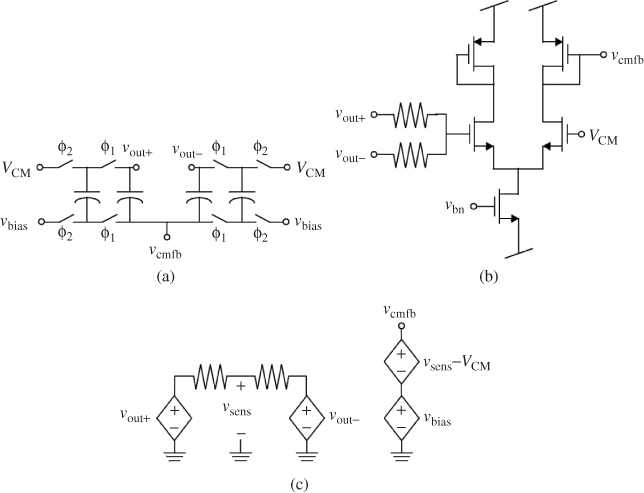
SC CMFB nets are often preferred in SC-![]() Ms to CT counterparts, as their design is straightforward, they lead to very small area overhead, and have no static power consumption. Conversely, although designing a CT CMFB net is usually not difficult, it leads to additional power consumption and involves a static inner feedback loop with sufficient gain that affects the dynamic response of the overall amplifier.
Ms to CT counterparts, as their design is straightforward, they lead to very small area overhead, and have no static power consumption. Conversely, although designing a CT CMFB net is usually not difficult, it leads to additional power consumption and involves a static inner feedback loop with sufficient gain that affects the dynamic response of the overall amplifier.
For the sake of completeness, Figure 4.42c shows an ideal CMFB net that can be employed together with the amplifier in Figure 4.41 for simulation purposes. Note that operation principle of the CMFB net is just macromodeled using voltage-controlled sources.
Characterization of the Amplifier in AC
Figure 4.43 shows the HSPICE netlist of the folded cascode amplifier in Figure 4.41. The included transistor-level sizing corresponds to an amplifier designed for an SC-![]() M implemented in a 0.13-
M implemented in a 0.13-![]() m CMOS process with 3.3-V supply [28]. The netlist includes the simulation test bench depicted in Figure 4.44a for the electrical characterization of the amplifier performance in an open-loop AC analysis, namely:
m CMOS process with 3.3-V supply [28]. The netlist includes the simulation test bench depicted in Figure 4.44a for the electrical characterization of the amplifier performance in an open-loop AC analysis, namely:
- DC gain (denoted as Av in the measurements section at the end of the netlist)
- Three decibel loss frequency (denoted as f3dB)
- Gain-bandwidth product (denoted as GB)
- Unity-gain bandwidth (denoted as UGBW)
- Phase margin (denoted as PM)
 noise component
- Thermal noise component
- Noise corner frequency
Figure 4.43 HSPICE netlist for the AC characterization of the folded cascode amplifier in Figure 4.41.
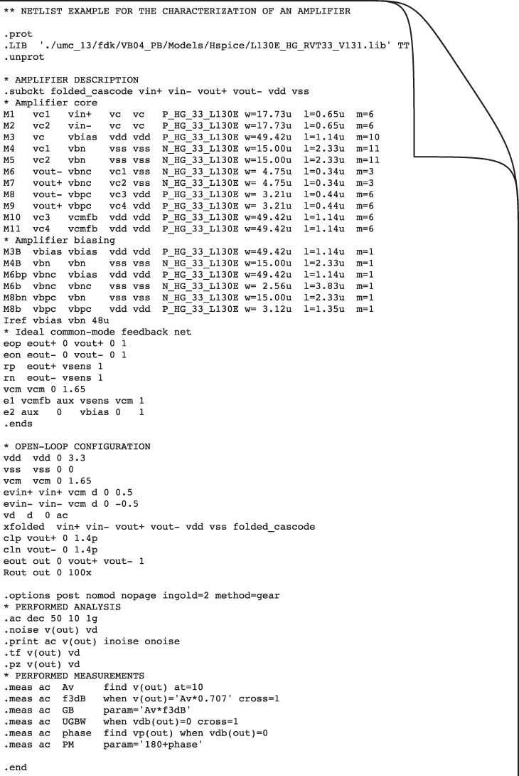
Figure 4.44 Amplifier simulation results obtained from an AC analysis in HSPICE: (a) test-bench circuit, (b) open-loop amplifier frequency response, and (c) input-referred noise PSD.

For that purpose an AC differential input signal is applied to the amplifier and its differential output voltage (![]() ) is computed. The test bench includes an ideal CMFB net as that shown in Figure 4.42c, as well as loading capacitors
) is computed. The test bench includes an ideal CMFB net as that shown in Figure 4.42c, as well as loading capacitors ![]() at the amplifier output nodes. The value of
at the amplifier output nodes. The value of ![]() (1.4 pF in the netlist in Figure 4.43) corresponds to an estimation of the equivalent amplifier load during the integration phase—
(1.4 pF in the netlist in Figure 4.43) corresponds to an estimation of the equivalent amplifier load during the integration phase—![]() in Equation 2.16.
in Equation 2.16.
Figure 4.44b shows the simulated frequency response of the amplifier gain, in which ![]() ,
, ![]() , and UGBW are identified. Their measured values are
, and UGBW are identified. Their measured values are ![]() ,
, ![]() , and
, and ![]() . The amplifier GB can be obtained from the
. The amplifier GB can be obtained from the ![]() product and equals
product and equals ![]() , that is, GB
, that is, GB ![]() UGBW, which is characteristic of a single-stage amplifier with a clearly dominant pole and results in a large phase margin (
UGBW, which is characteristic of a single-stage amplifier with a clearly dominant pole and results in a large phase margin (![]() in this case).
in this case).
Figure 4.44c shows the simulated PSD of the input-referred amplifier noise, in which the flicker and white components can be clearly identified, as well as the corner frequency (around 600 kHz in this case). Note that, as discussed in Section 4.2, the obtained PSD curve can also be used for generating a colored noise data sequence that captures the amplifier noise frequency response and injecting it in transient electrical simulations of the ![]() M.
M.
Characterization of the Amplifier in DC
Figure 4.45a illustrates a simulation test bench that allows to obtain the amplifier ![]() –
–![]() transfer characteristic and easily extract the amplifier transconductance
transfer characteristic and easily extract the amplifier transconductance ![]() and maximum output current
and maximum output current ![]() . For that purpose a DC differential signal ranging from
. For that purpose a DC differential signal ranging from ![]() to
to ![]() is applied at the amplifier input, while its output nodes are fixed to the common-mode level through voltage sources whose current is measured.
is applied at the amplifier input, while its output nodes are fixed to the common-mode level through voltage sources whose current is measured.
Figure 4.45 Amplifier simulation results obtained from a DC analysis in HSPICE: (a) test-bench circuit and (b) ![]() –
–![]() transfer characteristic, and (c) transconductance versus input voltage.
transfer characteristic, and (c) transconductance versus input voltage.

Figure 4.45b shows the simulated differential output current (![]() ) of the folded cascode amplifier in Figure 4.43 versus the differential input voltage
) of the folded cascode amplifier in Figure 4.43 versus the differential input voltage ![]() . From it the maximum amplifier output current can be measured (
. From it the maximum amplifier output current can be measured (![]() in this case).
in this case).
The amplifier transconductance DC characteristic can be easily obtained from the slope of the ![]() –
–![]() curve in the Figure 4.45b by simply computing
curve in the Figure 4.45b by simply computing ![]() . The resulting curve is depicted in Figure 4.45c, from which the amplifier transconductance at the quiescent point
. The resulting curve is depicted in Figure 4.45c, from which the amplifier transconductance at the quiescent point ![]() can be derived (
can be derived (![]() −1 in this example).9
−1 in this example).9
Characterization of the Amplifier Gain Nonlinearity
Figure 4.46a illustrates a different DC simulation test bench for extracting in this case the amplifier voltage transfer characteristic. From it the amplifier output swing OS and amplifier DC gain nonlinearity can be easily derived. For that purpose a DC differential signal ranging from ![]() to
to ![]() is again applied at the amplifier input, but with no loading conditions at its output nodes.
is again applied at the amplifier input, but with no loading conditions at its output nodes.
Figure 4.46 Amplifier simulation results obtained from a DC analysis in HSPICE: (a) test-bench circuit, (b) open-loop voltage transfer characteristic, and (c) amplifier gain versus output voltage.

Figure 4.46b shows the simulated differential output voltage (![]() ) versus the differential input voltage
) versus the differential input voltage ![]() for the folded cascode amplifier in Figure 4.43.
for the folded cascode amplifier in Figure 4.43.
The dependency of the amplifier gain on the output voltage level can be easily obtained from the data contained in the Figure 4.46b, just by computing ![]() from the curve and depicting the results against
from the curve and depicting the results against ![]() (instead of
(instead of ![]() ). Figure 4.46c shows the resulting gain curve for the folded cascode amplifier in the example, from which the DC gain at the quiescent point
). Figure 4.46c shows the resulting gain curve for the folded cascode amplifier in the example, from which the DC gain at the quiescent point ![]() can also be derived (
can also be derived (![]() , in accordance to low-frequency AC results in Figure 4.44b).
, in accordance to low-frequency AC results in Figure 4.44b).
Finally, note that the amplifier voltage characteristic in Figure 4.46b can be obtained from a relatively coarse DC sweep of the input voltage, whereas a very fine sweep is required to accurately obtain the amplifier gain curve in Figure 4.46c. For the sake of illustration, the DC input voltage was varied from ![]() to
to ![]() V in 10-mV steps to obtain the graphical representation in Figure 4.46b, whereas the DC simulation was run again with steps of only 50
V in 10-mV steps to obtain the graphical representation in Figure 4.46b, whereas the DC simulation was run again with steps of only 50 ![]() V (but only from
V (but only from ![]() to
to ![]() V) to have enough granularity in the
V) to have enough granularity in the ![]() axis in the results shown in Figure 4.46c.
axis in the results shown in Figure 4.46c.
4.4.3 Design Considerations of Transconductors
As already stated in this book, transconductors are essential building blocks of CT-![]() Ms. They are used for building Gm-C integrators and also to implement
Ms. They are used for building Gm-C integrators and also to implement ![]() M loop-filter coefficients. As an illustration, Figure 4.47 shows two different common examples of CT-
M loop-filter coefficients. As an illustration, Figure 4.47 shows two different common examples of CT-![]() M implementations. The first one, shown in Figure 4.47a, uses a front-end active-RC integrator, whereas the rest of loop-filter integrators are implemented using Gm-C topologies. This approach is normally chosen because of the better linearity performance achieved by active-RC integrators as compared with Gm-C integrators. If the linearity specification is not very restrictive, purely Gm-C implementations similar to that shown in Figure 4.47b are usually preferred because of their potential faster operation. Note that in both examples depicted in Figure 4.47, loop-filter coefficients are implemented using transconductors.
M implementations. The first one, shown in Figure 4.47a, uses a front-end active-RC integrator, whereas the rest of loop-filter integrators are implemented using Gm-C topologies. This approach is normally chosen because of the better linearity performance achieved by active-RC integrators as compared with Gm-C integrators. If the linearity specification is not very restrictive, purely Gm-C implementations similar to that shown in Figure 4.47b are usually preferred because of their potential faster operation. Note that in both examples depicted in Figure 4.47, loop-filter coefficients are implemented using transconductors.
Figure 4.47 Illustrating the use of transconductors in a third-order, single-loop CT-![]() M, considering: (a) an active-RC front-end integrator and (b) a Gm-C front-end integrator.
M, considering: (a) an active-RC front-end integrator and (b) a Gm-C front-end integrator.

The main electrical characteristics affecting the performance of transconductors used in ![]() Ms are the following: input/output swing, transconductance value and tuning range, finite DC gain, finite GB, mismatch error, and nonlinearity (usually characterized by the IIP3 parameter). The limit values of these design specifications are derived from behavioral system-level simulations that are further fine-tuned using macromodel electrical simulations as described in Section 4.1. Once these specifications have been clearly identified, a proper circuit topology is chosen and designed at the transistor level in order to meet them.
Ms are the following: input/output swing, transconductance value and tuning range, finite DC gain, finite GB, mismatch error, and nonlinearity (usually characterized by the IIP3 parameter). The limit values of these design specifications are derived from behavioral system-level simulations that are further fine-tuned using macromodel electrical simulations as described in Section 4.1. Once these specifications have been clearly identified, a proper circuit topology is chosen and designed at the transistor level in order to meet them.
Obviously, there are plenty of different transconductor circuits that can be used for implementing the loop filter of CT-![]() Ms. The detailed explanation of all of them is beyond the scope of this book. Instead, the following sections focus on two circuit examples. One of them is suited for the implementation of front-end, Gm-C integrators, while the other one is more appropriate to build Gm-C integrators embedded in the loop filter.
Ms. The detailed explanation of all of them is beyond the scope of this book. Instead, the following sections focus on two circuit examples. One of them is suited for the implementation of front-end, Gm-C integrators, while the other one is more appropriate to build Gm-C integrators embedded in the loop filter.
Example of Front-End Transconductor
One of the main limiting factors in open-loop Gm-C integrators is their poor linearity. Indeed, this is especially critical at the input node of ![]() Ms because harmonic distortion caused by the front-end
Ms because harmonic distortion caused by the front-end ![]() /
/![]() transconductor is directly translated to the digital domain without any attenuation. Thus, special emphasis should be put to design the front-end transconductor with high enough linearity, because it can severely degrade the performance of the modulator.
transconductor is directly translated to the digital domain without any attenuation. Thus, special emphasis should be put to design the front-end transconductor with high enough linearity, because it can severely degrade the performance of the modulator.
Figure 4.48 shows an example of front-end transconductor [29]. The circuit combines gain boosting techniques with resistive source degeneration in order to increase the linearity of the transconductance. Note that in this example, nMOS transistors are used in the input differential pair because a triple-well option is available in the technology where the transconductor is going to be integrated. This way, the MOS body effect can be avoided by simply connecting the source terminal to the substrate terminal. Otherwise, if the triple-well option is not available, pMOS transistors should be used for the differential input pair.
Figure 4.48 Example of ![]() M front-end transconductor with enhanced linearity [29].
M front-end transconductor with enhanced linearity [29].

As an example, let us consider that the circuit is placed at the front-end of a cascade 3-2 CT-![]() M with a front-end stage similar to that shown in Figure 4.47b, and that this modulator is intended to digitize 20-MHz signals with 12-bit effective resolution. According to behavioral simulations carried out in SIMSIDES, the following specifications are obtained for the front-end transconductor:
M with a front-end stage similar to that shown in Figure 4.47b, and that this modulator is intended to digitize 20-MHz signals with 12-bit effective resolution. According to behavioral simulations carried out in SIMSIDES, the following specifications are obtained for the front-end transconductor:
- Finite DC gain:
 70 dB
70 dB - Differential input/output swing: 0.3 V
- Third-order nonlinearity:
 86 dB.
In addition to the above specifications, input-referred thermal noise must be kept low enough not to degrade the effective resolution (12 bit) required by the modulator. Moreover, according to the synthesis of the ![]() M loop-filter coefficients, in this example the nominal input
M loop-filter coefficients, in this example the nominal input ![]() transconductance was chosen to be
transconductance was chosen to be ![]() A and the integration capacitance is 3.65 pF.
A and the integration capacitance is 3.65 pF.
In order to design the circuit in Figure 4.48 to cope with the above specifications, basic OTA design equations for the nominal transconductance, finite DC gain, SR, and GB are usually derived by hand [30] and used as initial point for the electrical design. Transistors are biased and sized in the saturation region using these by-hand equations and considering the voltage limits specified by the input/output swing. This initial design is fine tuned by electrical simulation in order to satisfy the required specifications with minimum power consumption. In addition, as in other essential ![]() M building blocks, the circuit must be simulated considering the effect of technology corners and mismatch deviations. The circuit in Figure 4.48 was designed in a
M building blocks, the circuit must be simulated considering the effect of technology corners and mismatch deviations. The circuit in Figure 4.48 was designed in a ![]() -
-![]() m CMOS technology to cope with the aforementioned specifications, achieving a DC gain of 73.8 dB, a maximum differential input/output swing of 0.3 V and
m CMOS technology to cope with the aforementioned specifications, achieving a DC gain of 73.8 dB, a maximum differential input/output swing of 0.3 V and ![]() dB, considering a single 1.2-V supply voltage [29].
dB, considering a single 1.2-V supply voltage [29].
Example of Loop-Filter Transconductor
Figure 4.49 shows an example of a transconductor (with its corresponding CMFB circuit) that can be used for building the loop-filter coefficients of CT-![]() Ms [29]. High-speed operation is achieved by using only feed-forward paths. These paths introduce a high frequency zero that extends the frequency range. The circuit uses a quadratic-term cancellation technique in order to improve the linearity of the transconductance. The basic idea behind this technique is to include an additional tail current source having its current in a quadratic dependence on the input signal, as conceptually illustrated in Figure 4.49. It can be shown that thequadratic term of the drain current of the differential-pair transistors can be cancellated if
Ms [29]. High-speed operation is achieved by using only feed-forward paths. These paths introduce a high frequency zero that extends the frequency range. The circuit uses a quadratic-term cancellation technique in order to improve the linearity of the transconductance. The basic idea behind this technique is to include an additional tail current source having its current in a quadratic dependence on the input signal, as conceptually illustrated in Figure 4.49. It can be shown that thequadratic term of the drain current of the differential-pair transistors can be cancellated if ![]() , where
, where ![]() is a gain factor that takes into account any signal scaling that may be applied to the input signal, and
is a gain factor that takes into account any signal scaling that may be applied to the input signal, and ![]() and
and ![]() stand for the large-signal transconductances of the input differential-pair transistor (
stand for the large-signal transconductances of the input differential-pair transistor (![]() ) and the extra MOS transistor added (
) and the extra MOS transistor added (![]() ), respectively.
), respectively.
Figure 4.49 Example of ![]() M loop-filter transconductor with quadratic-term cancellation technique [29].
M loop-filter transconductor with quadratic-term cancellation technique [29].

A very critical design consideration that must be taken into account in the design of CT-![]() M loop-filter circuit elements is their tunability. Thus, transconductors must be designed so that they can be tuned in order to keep the loop-filter time constants (
M loop-filter circuit elements is their tunability. Thus, transconductors must be designed so that they can be tuned in order to keep the loop-filter time constants (![]() ) unchanged over technology parameter variations. To this purpose, a circuit tuning strategy must be incorporated in the loop-filter transconductors in order to make the design of CT-
) unchanged over technology parameter variations. To this purpose, a circuit tuning strategy must be incorporated in the loop-filter transconductors in order to make the design of CT-![]() Ms feasible and robust against circuit element tolerances. In the example shown in Figure 4.49, the transconductance can be tuned through the tail bias current
Ms feasible and robust against circuit element tolerances. In the example shown in Figure 4.49, the transconductance can be tuned through the tail bias current ![]() . Note that, for voltage headroom reasons, this current source is connected between the positive supply voltage and the common source node. Thus, a variation of
. Note that, for voltage headroom reasons, this current source is connected between the positive supply voltage and the common source node. Thus, a variation of ![]() —through bias voltages named
—through bias voltages named ![]() —changes the value of the nominal transconductance, without significantly affecting the linearity of the transconductor.
—changes the value of the nominal transconductance, without significantly affecting the linearity of the transconductor.
Note that for the tuning to be effective, each transconductance of the ![]() M is usually implemented as the parallel connection of unit transconductors and a number of Monte Carlo simulations are required in order to guarantee that the performance of the transconductors—particularly the linearity—is not affected by the mismatch. In this example, a unit transconductance of
M is usually implemented as the parallel connection of unit transconductors and a number of Monte Carlo simulations are required in order to guarantee that the performance of the transconductors—particularly the linearity—is not affected by the mismatch. In this example, a unit transconductance of ![]() A V
A V![]() was used, while the values of
was used, while the values of ![]() ranged from
ranged from ![]() A to
A to ![]() A.
A.
As stated in the previous section, the linearity and gain specifications are not so demanding as in this case of front-end integrators. For instance, considering the same modulator specifications described in the previous section, the electrical specifications of the loop-filter transconductors will vary depending on their position in the modulator chain. The most restrictive specifications are the following:
- Finite DC gain:
 50 dB
50 dB - Differential input/output swing: 0.3 V
- Third-order nonlinearity:
 56 dB.
As an illustration, Figure 4.50 shows some typical characteristics obtained by electrical simulation of transconductors using the test-bench schematic shown in Figure 4.51. Figure 4.50a shows the output current as a function of the input current for different values of ![]() ranging from
ranging from ![]() A to
A to ![]() A in this example. The linearity of the transconductance can be calculated by computing the derivative of this
A in this example. The linearity of the transconductance can be calculated by computing the derivative of this ![]() –
–![]() characteristic. This is represented in Figure 4.50b. Following this procedure, the maximum transconductance variation for each of the values of
characteristic. This is represented in Figure 4.50b. Following this procedure, the maximum transconductance variation for each of the values of ![]() can be calculated. In this example, a deviation below
can be calculated. In this example, a deviation below ![]() is obtained in all cases within the specified input voltage range (0.3 V).
is obtained in all cases within the specified input voltage range (0.3 V).
Figure 4.50 Illustrating the electrical performance of ![]() M loop-filter transconductors: (a) output current versus input voltage for different values of the tuning current
M loop-filter transconductors: (a) output current versus input voltage for different values of the tuning current ![]() and (b) transconductance versus input voltage.
and (b) transconductance versus input voltage. ![]() ranges from
ranges from ![]() A to
A to ![]() A.
A.
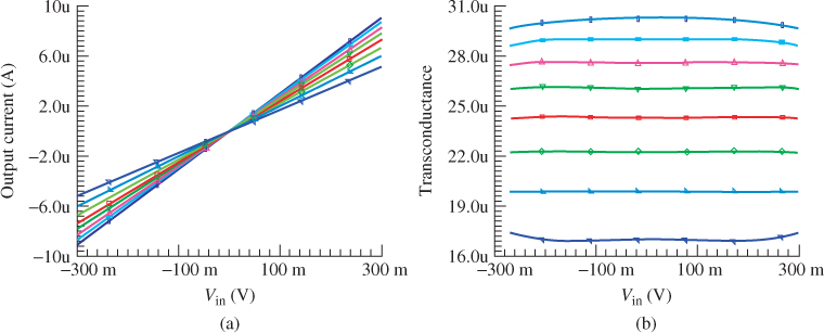
Figure 4.51 Test-bench schematic used for characterizing the ![]() M loop-filter transconductors. Note that this test bench can be used for DC, AC, and transient analysis. Alternatively, a load circuit can be connected at the output of the transconductor in order to emulate a circuit environment closer to the actual situation of loop-filter transconductors embedded in a CT-
M loop-filter transconductors. Note that this test bench can be used for DC, AC, and transient analysis. Alternatively, a load circuit can be connected at the output of the transconductor in order to emulate a circuit environment closer to the actual situation of loop-filter transconductors embedded in a CT-![]() M.
M.

Figure 4.52 shows the frequency response of a Gm-C integrator made up of a unit transconductor (with a nominal transconductance of ![]() A V
A V![]() ) and the unit integration capacitor (3.65 pF in this example). Note that the phase error at unity gain of the integrator is below
) and the unit integration capacitor (3.65 pF in this example). Note that the phase error at unity gain of the integrator is below ![]() , while the high-frequency poles are placed at a much higher frequency than the GB of the integrator. This is due to the fact that the transconductor in Figure 4.49 is essentially composed of feed-forward paths, which facilitates a higher speed of operation.
, while the high-frequency poles are placed at a much higher frequency than the GB of the integrator. This is due to the fact that the transconductor in Figure 4.49 is essentially composed of feed-forward paths, which facilitates a higher speed of operation.
Figure 4.52 Phase and gain response of the loop-filter (unit) transconductor in Figure 4.49.

4.4.4 Design Considerations of Comparators
Comparators are essential building blocks of ![]() ADCs. These circuits are used for building the quantizer embedded in the modulator. Because of their position in the modulator loop, the comparator specifications are not very demanding in most practical cases, as circuit errors are attenuated by NTF in the same way as the quantization noise. However, the design of main performance limitations (i.e., offset, hysteresis, and comparison time) must be carefully taken into account in order to optimize the performance of
ADCs. These circuits are used for building the quantizer embedded in the modulator. Because of their position in the modulator loop, the comparator specifications are not very demanding in most practical cases, as circuit errors are attenuated by NTF in the same way as the quantization noise. However, the design of main performance limitations (i.e., offset, hysteresis, and comparison time) must be carefully taken into account in order to optimize the performance of ![]() Ms. Typical static specifications require an offset and a hysteresis in the order of tens of millivolts, and a maximum comparison time of
Ms. Typical static specifications require an offset and a hysteresis in the order of tens of millivolts, and a maximum comparison time of ![]() of the clock period, that is, around one half of the time interval corresponding to the strobe phase.10 These specifications can be achieved by using the so-called regenerative latch topologies described in the following subsection.
of the clock period, that is, around one half of the time interval corresponding to the strobe phase.10 These specifications can be achieved by using the so-called regenerative latch topologies described in the following subsection.
Regenerative Latch-Based Comparators
The majority of comparator circuits used in ![]() Ms are based on a DT positive-feedback regenerative latch that is built by cross-coupling a pair of inverters as conceptually depicted in Figure 4.53a [31]. The inverters amplify the differential input voltage
Ms are based on a DT positive-feedback regenerative latch that is built by cross-coupling a pair of inverters as conceptually depicted in Figure 4.53a [31]. The inverters amplify the differential input voltage ![]() to obtain the saturated differential output
to obtain the saturated differential output ![]() , according to the characteristics drawn in Figure 4.53b. During the so-called reset phase (
, according to the characteristics drawn in Figure 4.53b. During the so-called reset phase (![]() high), the differential input is stored in the input sampling capacitors
high), the differential input is stored in the input sampling capacitors ![]() and the circuit is driven to the central state
and the circuit is driven to the central state ![]() (Figure 4.53b). During the comparison or strobe phase (
(Figure 4.53b). During the comparison or strobe phase (![]() high), the differential input is retrieved, forcing an initial state either on the right (
high), the differential input is retrieved, forcing an initial state either on the right (![]() or on the left (
or on the left (![]() of
of ![]() . From this initial state, the action of positive feedback forces the output to evolve either toward
. From this initial state, the action of positive feedback forces the output to evolve either toward ![]() (for
(for ![]() ) or toward
) or toward ![]() (for
(for ![]() ). In both cases, the dynamic evolution around the central point is realized at a high speed due to the action of positive feedback.
). In both cases, the dynamic evolution around the central point is realized at a high speed due to the action of positive feedback.
Figure 4.53 Positive-feedback regenerative latch: (a) conceptual schematic and (b) illustration of dynamic trajectories in the input–output characteristic.

Figure 4.54 shows some regenerative latch CMOS circuits [32–35] that are commonly used for implementing comparators in state-of-the-art ![]() Ms, all of them based on the conceptual model shown in Figure 4.53a. In practice, the static resolution of all these circuits is limited by dissymmetries between the positive and the negative branches of the fully-differential circuit, as well as other second-order circuit phenomena such as the kick-back noise on the integrator connected to the comparator. Thus, a preamplifier is usually placed at the input of the regenerative latch in order to improve the static resolution of these kinds of comparators [36].
Ms, all of them based on the conceptual model shown in Figure 4.53a. In practice, the static resolution of all these circuits is limited by dissymmetries between the positive and the negative branches of the fully-differential circuit, as well as other second-order circuit phenomena such as the kick-back noise on the integrator connected to the comparator. Thus, a preamplifier is usually placed at the input of the regenerative latch in order to improve the static resolution of these kinds of comparators [36].
Figure 4.54 Examples of CMOS latches frequently used in ![]() Ms: (a) [32], (b) [33], (c) [34], and (d) [35].
Ms: (a) [32], (b) [33], (c) [34], and (d) [35].

Figure 4.55 shows a typical example of a CMOS regenerative latch comparator with preamplifier.11 It consists of a pMOS differential input pair (![]() ), a CMOS regenerative latch circuit, and a set-reset (SR) flip-flop to store the voltage provided by the latch. The latch circuit is composed of an nMOS flip-flop (
), a CMOS regenerative latch circuit, and a set-reset (SR) flip-flop to store the voltage provided by the latch. The latch circuit is composed of an nMOS flip-flop (![]() ) with a pair of nMOS switches (
) with a pair of nMOS switches (![]() ) for strobing and an nMOS switch (
) for strobing and an nMOS switch (![]() ) for resetting, and a pMOS flip-flop (
) for resetting, and a pMOS flip-flop (![]() ) with a pair of pMOS precharge switches (
) with a pair of pMOS precharge switches (![]() ).
).
Figure 4.55 Example of a typical CMOS regenerative latch comparator with preamplifier.

The operation of the circuit in Figure 4.55 is as follows: During clock phase ![]() (reset phase), the latch is in reset mode and the input differential pair injects a current proportional to the differential input voltage (
(reset phase), the latch is in reset mode and the input differential pair injects a current proportional to the differential input voltage (![]() ), which generates an initial voltage imbalance across the on-resistance of switch
), which generates an initial voltage imbalance across the on-resistance of switch ![]() . The voltage difference across
. The voltage difference across ![]() is amplified when the latch becomes enabled during the comparison (amplification) phase
is amplified when the latch becomes enabled during the comparison (amplification) phase ![]() , achieving a very fast comparison time due to the action of positive feedback.
, achieving a very fast comparison time due to the action of positive feedback.
Design Guidelines
The design of the comparators used in ![]() Ms is carried out according to the high-level specifications extracted from behavioral simulations as described in Chapter 3. The main design parameters included in the behavioral models, which degrade the performance of
Ms is carried out according to the high-level specifications extracted from behavioral simulations as described in Chapter 3. The main design parameters included in the behavioral models, which degrade the performance of ![]() Ms, are essentially two static parameters, namely, offset and hysteresis. In addition, the transient response of the comparator must be fast enough to complete their operation within the comparison clock phase. Therefore, the analog sections12 of the comparator (i.e., the preamplifier and the latch) must be carefully sized accordingly to these specifications.
Ms, are essentially two static parameters, namely, offset and hysteresis. In addition, the transient response of the comparator must be fast enough to complete their operation within the comparison clock phase. Therefore, the analog sections12 of the comparator (i.e., the preamplifier and the latch) must be carefully sized accordingly to these specifications.
The preamplifier aims to fulfill several goals, namely, to obtain a high DC gain in order to reduce the comparator input-referred offset, a low kick-back noise, and high speed, while keeping low parasitic input capacitances. Therefore, the increase of the preamplifier DC gain should not be done exclusively by increasing the size of the input differential-pair transistor—in order to increase ![]() —for a given bias current, because this would also increase the input parasitic capacitance. This design trade-off can be solved using a preamplifier schematic with a high output resistance similar to that shown in Figure 4.56. In this circuit, transistors
—for a given bias current, because this would also increase the input parasitic capacitance. This design trade-off can be solved using a preamplifier schematic with a high output resistance similar to that shown in Figure 4.56. In this circuit, transistors ![]() and
and ![]() are biased in the ohmic region and hence used as resistors to increase the output resistance of the preamplifier.
are biased in the ohmic region and hence used as resistors to increase the output resistance of the preamplifier.
Figure 4.56 Single-stage preamplifier with ohmic-biased transistors (![]() and
and ![]() ) to increase the output resistance.
) to increase the output resistance.

Another important design trade-off that takes place in the latch involves the required mismatch specifications (which have a direct effect on the static resolution) and the comparator speed. This way, using minimum sizes for the inverter transistors (![]() in Figure 4.55) minimizes the MOS parasitic capacitances, thus benefiting the transient response. However, minimum-sized transistors increase the sensitivity to technology process variations.
in Figure 4.55) minimizes the MOS parasitic capacitances, thus benefiting the transient response. However, minimum-sized transistors increase the sensitivity to technology process variations.
A minimum length should be used for the switches involved (![]() in Figure 4.55) in order to reduce the switch on-resistance as well as the effect of charge injection. Note that the input voltage difference is sensed across switch
in Figure 4.55) in order to reduce the switch on-resistance as well as the effect of charge injection. Note that the input voltage difference is sensed across switch ![]() , and hence its on-resistance becomes critical for a correct operation of the comparator. Indeed, the performance of the latch is very sensitive to the size of
, and hence its on-resistance becomes critical for a correct operation of the comparator. Indeed, the performance of the latch is very sensitive to the size of ![]() , that has motivated some designers to use more robust topologies.
, that has motivated some designers to use more robust topologies.
This is the case of the latch shown in Figure 4.54d [35]. The operation of this circuit is governed by one clock phase, named ![]() in the figure. Thus, when strobe or amplification clock signal (
in the figure. Thus, when strobe or amplification clock signal (![]() ) triggers to a logic one, switch
) triggers to a logic one, switch ![]() turns on and transistors
turns on and transistors ![]() will process the differential output of the preamplifier. After a short time, one of the input differential-pair transistors will turn off depending on the sign of the input voltage imbalance, thus creating a differential voltage between nodes
will process the differential output of the preamplifier. After a short time, one of the input differential-pair transistors will turn off depending on the sign of the input voltage imbalance, thus creating a differential voltage between nodes ![]() and
and ![]() . Meanwhile,
. Meanwhile, ![]() and
and ![]() will turn on and, later, the cross-coupled scheme will start working, leading to a fast regeneration of the initial voltage imbalance [9].
will turn on and, later, the cross-coupled scheme will start working, leading to a fast regeneration of the initial voltage imbalance [9].
Although regenerative latch comparators are very fast, the comparison time and the dynamic resolution must be properly characterized at transistor level. The following sections give some practical ways to do this task.
Characterization of Offset and Hysteresis Based on the Input-Ramp Method
Comparator offset and hysteresis can be characterized in electrical simulations using the test-bench circuit shown in Figure 4.57a. A slow ramp-waveform input signal is applied to the comparator, so that the offset and hysteresis parameters can be extracted from the output voltage waveform as conceptually depicted in Figure 4.57b. Note that in order to obtain a more precise value of both performance metrics (offset and hysteresis), the voltage limits of the input ramp should be approximately of the same order as the specified offset and hysteresis.
Figure 4.57 Characterization of offset and hysteresis based on the input-ramp method: (a) Cadence Virtuoso test-bench schematic and (b) conceptual output response and computation of offset and hysteresis parameters.

Let us consider an example in which the target specifications for the offset and the hysteresis are ![]() and
and ![]() mV, respectively. In order to take into account the impact of mismatch and technology parameter variations, a large number of simulations considering all technology corners as well as a Monte Carlo analysis should be carried out. As an illustration, Figure 4.58 shows some typical output waveforms obtained in HSPICE for the characterization of the offset and hysteresis.
mV, respectively. In order to take into account the impact of mismatch and technology parameter variations, a large number of simulations considering all technology corners as well as a Monte Carlo analysis should be carried out. As an illustration, Figure 4.58 shows some typical output waveforms obtained in HSPICE for the characterization of the offset and hysteresis.
Figure 4.58 Illustrating the electrical characterization of hysteresis in regenerative latch comparators. Monte Carlo simulation in HSPICE.

The method based on the input ramp does not allow for memory or hysteresis issues in the comparator operation because the voltage value of the input signal is always increasing (or decreasing) in amplitude, which is not common in practice. A more realistic test bench consists of using a sinusoidal or triangular input signal. This way, the input signal is forced to take alternating signs in order to allow for memory effects [9].
Another disadvantage of the ramp-waveform, test-bench method is that a slower ramp is needed to obtain the required accuracy in the characterization of the offset and the hysteresis. The slower the input ramp is, the longer the transient simulation, which might lead to long CPU times, as typically 100–200 simulations are needed for an accurate Monte Carlo simulation.
Characterization of Offset and Hysteresis Based on the Bisectional Method
A more efficient way of characterizing the input offset of the comparator is based on the so-called bisectional method. In this method, graphically illustrated in Figure 4.59, a root-finding algorithm works by repeatedly halving an interval and then selecting the subinterval in which the root exists [37]. Given two points, ![]() and
and ![]() , such that
, such that ![]() and
and ![]() have opposite signs, the intermediate value theorem says that
have opposite signs, the intermediate value theorem says that ![]() must have at least one root in the interval
must have at least one root in the interval ![]() as long as
as long as ![]() is continuous. Thus, the bisection algorithm is then applied to the subinterval where the sign change occurs until a solution under a defined tolerance is obtained. It can be shown that the number of iterations required to reach convergence with a tolerance error
is continuous. Thus, the bisection algorithm is then applied to the subinterval where the sign change occurs until a solution under a defined tolerance is obtained. It can be shown that the number of iterations required to reach convergence with a tolerance error ![]() is
is ![]() [37].
[37].
Figure 4.59 Graphical illustration of the bisectional method algorithm.

Figure 4.60a shows the test bench used in Cadence Virtuoso Schematic editor for the comparator offset computation. The preamplifier and the regenerative latch are placed inside a feedback loop, in which the preamplifier input signal is controlled by a block that implements the bisectional algorithm described earlier. A Verilog-A code [1], shown in Figure 4.60b, is used for this purpose. The input of this block is the differential output of the regenerative latch, so the algorithm basically selects the next input voltage based on the comparator output, following the procedure depicted in Figure 4.59. Note that a delayed version of the strobe clock signal triggers the Verilog-A block corresponding to the bisectional algorithm. This time delay must be longer than the response time of the regenerative latch, but shorter than half of the cycle of the comparator strobe.
Figure 4.60 Test bench used for the characterization of the comparator offset based on the bisectional algorithm method: (a) Cadence Virtuoso Schematic and (b) Verilog-A code for the bisectional algorithm.

Characterizing the Comparison Time
Figure 4.61 illustrates the electrical simulation method that is usually followed to characterize the resolution speed and the comparison time of comparators. An input step of ![]() is applied, where
is applied, where ![]() is the specified static resolution of the comparator (
is the specified static resolution of the comparator (![]() mV in this example). The comparison time, also referred to as resolution time, is defined in this test bench as the time interval between the time instant in which the strobe phase becomes low at the end of the comparison phase and the time instant when the output reaches the corresponding logic level, that is,
mV in this example). The comparison time, also referred to as resolution time, is defined in this test bench as the time interval between the time instant in which the strobe phase becomes low at the end of the comparison phase and the time instant when the output reaches the corresponding logic level, that is, ![]() for a positive input step or
for a positive input step or ![]() otherwise. Monte Carlo and technology corner variations need to be checked and the worst-case values are usually taken as the design specification.
otherwise. Monte Carlo and technology corner variations need to be checked and the worst-case values are usually taken as the design specification.
Figure 4.61 Illustrating the characterization of comparison time in regenerative latch comparators.

4.4.5 Design Considerations of Current-Steering DACs
As already discussed earlier in this book, the DACs used in the feedback path of ![]() Ms are mainly implemented using SC and SI or current-steering circuit techniques.13 The design of SC feedback DACs involves taking into account considerations for the design of switches and capacitors according to the design criteria previously stated in this chapter and in Chapter 2. Indeed, the switches and capacitors used for building SC DACs are embedded in the SC integrators and quantizers (Figure 4.9). Thus, SC DACs do not require special attention apart from the design issues related to switches already discussed.
Ms are mainly implemented using SC and SI or current-steering circuit techniques.13 The design of SC feedback DACs involves taking into account considerations for the design of switches and capacitors according to the design criteria previously stated in this chapter and in Chapter 2. Indeed, the switches and capacitors used for building SC DACs are embedded in the SC integrators and quantizers (Figure 4.9). Thus, SC DACs do not require special attention apart from the design issues related to switches already discussed.
In contrast, CS DACs—mostly used in CT-![]() Ms—are essential building blocks affecting the performance of the modulator because of several nonideal circuit phenomena already discussed in Chapters 2 and 3, namely clock jitter error, transient response (and its effect on the excess loop delay error), and linearity (due to device mismatch of unit current sources). Indeed, CS DACs are specifically suited for wideband CT-
Ms—are essential building blocks affecting the performance of the modulator because of several nonideal circuit phenomena already discussed in Chapters 2 and 3, namely clock jitter error, transient response (and its effect on the excess loop delay error), and linearity (due to device mismatch of unit current sources). Indeed, CS DACs are specifically suited for wideband CT-![]() Ms because of their potential benefits in terms of high-speed operation and the convenience to interface with both Gm-C and active-RC CT-
Ms because of their potential benefits in terms of high-speed operation and the convenience to interface with both Gm-C and active-RC CT-![]() Ms [38]. This is illustrated in Figure 4.62 that shows a conceptual schematic of the input summing node of a CT-
Ms [38]. This is illustrated in Figure 4.62 that shows a conceptual schematic of the input summing node of a CT-![]() M. Note in Figure 4.62a that the output current of the feedback CS DAC is naturally14 added with the output current of the loop-filter Gm-C transconductor. In the case of active-RC implementations, the current-mode adding operation takes place at the virtual ground input node of the amplifier as illustrated in Figure 4.62b.
M. Note in Figure 4.62a that the output current of the feedback CS DAC is naturally14 added with the output current of the loop-filter Gm-C transconductor. In the case of active-RC implementations, the current-mode adding operation takes place at the virtual ground input node of the amplifier as illustrated in Figure 4.62b.
Figure 4.62 Illustrating the connection of CS DACs at the input summing node of (a) Gm-C ![]() Ms and (b) active-RC
Ms and (b) active-RC ![]() Ms.
Ms.

This section pays attention to the main design criteria usually taken into account in the design of CS DACs—from the circuit-level perspective—focusing on those issues that must be considered during the electrical (transistor-level) design of ![]() Ms. Special emphasis is put on their main performance metrics of CS DACs, showing how to characterize these metrics with practical test benches implemented in SPICE-like simulators.
Ms. Special emphasis is put on their main performance metrics of CS DACs, showing how to characterize these metrics with practical test benches implemented in SPICE-like simulators.
Fundamentals and Basic Concepts of CS DACs
Figure 4.63a and b show two conceptual schemes of a CS DAC [12], where the output current is obtained by adding a number of switched unit current cells together. The switches are controlled by the DAC input bits, which are in turn the outputs of the quantizer embedded in the ![]() M loop filter. Thus, if a binary code is used,
M loop filter. Thus, if a binary code is used, ![]() binary-weighted scaled current cells are required, as shown in Figure 4.63a. Note that, although this solution requires the minimum number of elements, they are more sensitive to device element mismatch, mainly because of the very different values of the cell currents. For that reason, a thermometer-coded CS DAC similar to that shown in Figure 4.63b is usually chosen to implement the feedback DACs of CT-
binary-weighted scaled current cells are required, as shown in Figure 4.63a. Note that, although this solution requires the minimum number of elements, they are more sensitive to device element mismatch, mainly because of the very different values of the cell currents. For that reason, a thermometer-coded CS DAC similar to that shown in Figure 4.63b is usually chosen to implement the feedback DACs of CT-![]() Ms. This approach relaxes the matching requirements at the price of exponentially increasing the number of unit elements, that is, the number of current cells and switches.
Ms. This approach relaxes the matching requirements at the price of exponentially increasing the number of unit elements, that is, the number of current cells and switches.
Figure 4.63 Conceptual schemes of switched-current DACs: (a) based on binary-weighted current cells, (b) based on thermometer-coded current cells, (c) single-ended current-steering DAC, and (d) fully-differential current-steering DAC.

Note that the circuit schemes shown in Figure 4.63a and b cannot be implemented in practice because of to the current glitches appearing when current cells are left open. For that reason, the scheme shown in Figure 4.63c—commonly referred to as current-steering—is usually preferred. In this approach, the currents provided by the cells are steered or redirected either to the DAC output summing node or to a dummy low-impedance node, by means of complementary switches.
The scheme in Figure 4.63c is particularly useful in fully-differential implementations, which is one of the most common situations in practice. In this case, conceptually depicted in Figure 4.63d, unit current cells are steered either to the positive or to the negative output current, depending on the corresponding input digital code.
Practical Implementation of CS DACs in  Ms
Ms
Figure 4.64a shows an alternative implementation to Figure 4.63d, which provides a fully-balanced (complementary) differential output current with maximized power efficiency. As conceptually highlighted in the figure, two different kinds of current cells, p-type and n-type, are used for providing the current sources and sinks needed. The main problem of this DAC topology is in achieving the required voltage headroom for both types of current cells.
Figure 4.64 Conceptual schemes of fully-balanced (complementary) current-steering DACs considering: (a) switchable p-type and n-type current cells, (b) fixed n-type current cells, (c) fixed p-type current cells, and (d) different output nodes for p-type and n-type current cells. P-type and n-type current cells are sometimes called current sources and current sinks, respectively.

In order to palliate this limitation, diverse DAC topologies have been proposed to relax the voltage headroom specification. The most common approach consists of keeping one of the current cell types fixed and the other switchable. This is conceptually illustrated in the CS DAC architectures depicted in Figure 4.64b and c. The former, which uses a fixed n-type current cell and switchable p-type current cells, allows a larger headroom for the (switchable) p-type current cells. The opposite situation is given in Figure 4.64c. In both cases, the power efficiency is reduced to ![]() . The choice of one of these two topologies will be conditioned by the voltage headroom requirement for each type of cells in a given design.
. The choice of one of these two topologies will be conditioned by the voltage headroom requirement for each type of cells in a given design.
Figure 4.64d shows a CS DAC architecture that keeps a power efficiency of ![]() with relaxed specifications for the voltage headroom of both types of current cells. In this approach, p-type and n-type current cells are connected to different nodes, which are strategically chosen to provide the highest headroom voltage for each type of cell. This approach was successfully proposed and implemented by the authors in [39]. In this case, illustrated in Figure 4.65, the p-type current cells are connected to the source node of the n-type cascode transistors of the Gm-C integrator output stage, while the p-type current cells are connected to the corresponding source terminal of the nMOS cascode transistors, maximizing thus the headroom for both types of cells. Note also that the source terminal of the cascode transistors provides a low-impedance node to the CS DAC output, thus reducing its output swing and making its design more robust [39].
with relaxed specifications for the voltage headroom of both types of current cells. In this approach, p-type and n-type current cells are connected to different nodes, which are strategically chosen to provide the highest headroom voltage for each type of cell. This approach was successfully proposed and implemented by the authors in [39]. In this case, illustrated in Figure 4.65, the p-type current cells are connected to the source node of the n-type cascode transistors of the Gm-C integrator output stage, while the p-type current cells are connected to the corresponding source terminal of the nMOS cascode transistors, maximizing thus the headroom for both types of cells. Note also that the source terminal of the cascode transistors provides a low-impedance node to the CS DAC output, thus reducing its output swing and making its design more robust [39].
Figure 4.65 Illustrating the use of CS DACs with p-type and n-type current cells connected at different nodes of Gm-C integrators as proposed in [39].

Current Cell Circuits, Error Limitations, and Design Criteria
The operation of CS DACs described above is degraded in practice by the effect of circuit implementation of switches and current cells. Among others, the main limiting factors15 affecting the performance of CS DACs in ![]() Ms are caused by random errors because of to device mismatch and systematic errors due to output impedance of the current cell, thermal gradients, layout edge effects, and incomplete settling error.
Ms are caused by random errors because of to device mismatch and systematic errors due to output impedance of the current cell, thermal gradients, layout edge effects, and incomplete settling error.
Therefore, current cells are designed to satisfy a number of design specifications that are derived from behavioral simulations. Some of these specifications involve the value of the output resistance, the transient response, mismatch, output swing, etc. Among others, there is usually a strong trade-off between the required cell mismatch and the settling time. Thus, in order to relax the mismatch requirements without penalizing the linearity of the modulator, linearization techniques—such as DEM or digital calibration—are used as described in Section 1.6.
Essentially, the following requirements should be taken into consideration for designing the current cells of CS DACs in CT-![]() Ms:
Ms:
- Reduce the mismatch among unit current cells.
- Increase the current cell output impedance, making use of cascode stages.
- Ensure that transistors operate in the saturation region for the specified integrator output swing. This is easier to achieve when
 M loop-filter integrators are active-RC, as the signal swing is limited at the virtual ground node of the OTA.
 - Reduce the clock feedthrough error, which can be controlled by keeping parasitic capacitances as low as possible. An additional strategy to reduce this error consists of minimizing the voltage difference between the switch on-state and the switch off-state. This technique—often referred to as soft-driving16 —reduces also the overshoot currents due to the clock-signal transitions and allows switches to operate also in the saturation region, thus acting as cascode transistors for further boosting the current cell output impedance.
- Reduce the CS DAC noise contribution to the required IBN specification of the modulator. Note that both thermal and flicker noise sources associatedwith current cells are summed at the
 M input node, thus constituting an ultimate limiting factor.
In order to cope with the aforementioned design criteria with optimized power consumption, a huge number of different current cell topologies have been proposed in the open literature for the implementation of CS DACs used in CT-![]() Ms. The circuit topologies span from basic cells—such as a single transistor—to simple cascode, regulated cascode, etc. The detailed description of all the different CS DAC current cell approaches goes beyond the scope of this book.
Ms. The circuit topologies span from basic cells—such as a single transistor—to simple cascode, regulated cascode, etc. The detailed description of all the different CS DAC current cell approaches goes beyond the scope of this book.
CS 4-bit DAC Example
As a case study, let us consider a CS 4-bit DAC based on the circuit topology shown in Figure 4.64c. It consists of two fixed p-type current sources and 15 (![]() ) n-type switchable current cells that are controlled through simple nMOS switches by a thermometer-coded input data. These data are entered into the DAC through a set of D-latches driving the switch gates as illustrated in Figure 4.66.
) n-type switchable current cells that are controlled through simple nMOS switches by a thermometer-coded input data. These data are entered into the DAC through a set of D-latches driving the switch gates as illustrated in Figure 4.66.
Figure 4.66 Illustrating the use of D-latches to connect the ![]() M quantizer output and the nMOS switches of CS DACs.
M quantizer output and the nMOS switches of CS DACs.

The 4-bit CS DAC was used for implementing the NRZ feedback DAC of a fifth-order cascade 3-2 Gm-C CT-![]() M intended to digitize 20-MHz signals with 12-bit effective resolution, with a sampling frequency of 240 MHz [29]. These modulator specifications were mapped onto building-block specifications using SIMSIDES as described in Section 3.6.2. As a result, the following specifications were defined for the CS DAC:
M intended to digitize 20-MHz signals with 12-bit effective resolution, with a sampling frequency of 240 MHz [29]. These modulator specifications were mapped onto building-block specifications using SIMSIDES as described in Section 3.6.2. As a result, the following specifications were defined for the CS DAC:
- Output resistance:
 M
M
- Settling time:
 ns
ns - Mismatch error:
 LSB.
LSB.
Among others, there is a strong design trade-off between the required mismatch error and the settling time error. This trade-off was relaxed in this design example by using DEM linearization techniques that reduced the mismatch requirement to ![]() LSB. The unit current cell was chosen to be
LSB. The unit current cell was chosen to be ![]() A, which leads to 360
A, which leads to 360 ![]() A (i.e.,
A (i.e., ![]() ) pMOS current sources.
) pMOS current sources.
Another important limitation of the CS DAC in this design example was caused by the headroom voltage required for the pMOS current cells. As the common-mode voltage of the modulator was set to 0.75 V (forced by a design requirement of the loop-filter transconductors) and the FS voltage range was 0.3 V, the headroom voltage for the pMOS and the nMOS current sources resulted in 0.3 and 0.6 V, respectively. In order to satisfy all these specifications, the gain-boosted pMOS current source similar to that shown in Figure 4.67a is considered, while regulated cascode topologies, depicted in Figure 4.67b, can be used for the nMOS current cells. These cells can be designed to satisfy the aforementioned specifications, while dissipating a reasonable power consumption of 0.49 and 0.1 mW, respectively, for the pMOS and the nMOS cell [29].
Figure 4.67 Examples of CS DAC current cells: (a) pMOS gain-boosted current cell and (b) nMOS regulated cascode current cell.

4.5 Auxiliary  M Building Blocks
As stated earlier in this chapter, in addition to the basic building blocks used for implementing the loop filter and the quantizer of a ![]() M, there are other subcircuits required to make an IC operative. This section overviews the most important blocks, showing their fundamental schematics as well as some practical considerations to take into account in their design.
M, there are other subcircuits required to make an IC operative. This section overviews the most important blocks, showing their fundamental schematics as well as some practical considerations to take into account in their design.
4.5.1 Clock-Phase Generators
As any sampled-data system, the operation of ![]() Ms is governed by a clock signal. Usually, CT-
Ms is governed by a clock signal. Usually, CT-![]() Ms require one clock signal and its complementary version. In contrast, SC-
Ms require one clock signal and its complementary version. In contrast, SC-![]() Ms need to divide the clock period into several time intervals or clock phases that are generated by a digital circuit, commonly referred to as clock-phase generator.
Ms need to divide the clock period into several time intervals or clock phases that are generated by a digital circuit, commonly referred to as clock-phase generator.
Phase Generation
Figure 4.68a and b show two well-known digital circuits frequently used for generating the clock phases needed in SC-![]() Ms. Essentially, the operation of both circuits is based on the use of bistable flip-flops to generate several periodic signals from an input signal, also named master clock. The scheme in Figure 4.68a consists of a feedback loop made up of two NAND gates, each one connected in series with a cascade of inverters. The number and sizes of these inverters provide the required clock-phase delays and nonoverlapping intervals.
Ms. Essentially, the operation of both circuits is based on the use of bistable flip-flops to generate several periodic signals from an input signal, also named master clock. The scheme in Figure 4.68a consists of a feedback loop made up of two NAND gates, each one connected in series with a cascade of inverters. The number and sizes of these inverters provide the required clock-phase delays and nonoverlapping intervals.
Figure 4.68 Conceptual schemes of clock-phase generators frequently used in SC-![]() Ms: (a) feedback loop made up of two NANDs and a cascade of inverters, (b) D-latch-based generator, and (c) master clock generated by an (on-chip) PLL frequency synthesizer and an (off-chip) crystal oscillator. The use of on-chip PLLs allows generation of high-frequency, high-precision (low-jitter) clock signals, usually at the price of increasing the power consumption.
Ms: (a) feedback loop made up of two NANDs and a cascade of inverters, (b) D-latch-based generator, and (c) master clock generated by an (on-chip) PLL frequency synthesizer and an (off-chip) crystal oscillator. The use of on-chip PLLs allows generation of high-frequency, high-precision (low-jitter) clock signals, usually at the price of increasing the power consumption.

Figure 4.68b shows an alternative implementation of the clock-phase generator, which is also based on the use of flip-flops [22]. In this case, there is no global feedback loop and the different clock phases are generated by connecting D-type latches in cascade to provide the required delays and inversions.
In some high-frequency applications that demand a very high-precision, high-speed, and low-jitter, clock-phase scheme, the master clock signal used in Figure 4.68a and b is synthesized by an on-chip phase-locked loop (PLL) and an off-chip well-controlled crystal oscillator [40, 41], as conceptually depicted in Figure 4.68c.17
Note that both clock drivers in Figure 4.68a and b generate two nonoverlapped clock phases—![]() —that control the sampling and integration operations of SC integrators. Delayed versions of the clock phases—
—that control the sampling and integration operations of SC integrators. Delayed versions of the clock phases—![]() —are also generated in order to attenuate the error caused by signal-dependent charge injection produced during the turn-off process of input switches in SC integrators [43]. Complementary versions of the four clock phases—that is,
—are also generated in order to attenuate the error caused by signal-dependent charge injection produced during the turn-off process of input switches in SC integrators [43]. Complementary versions of the four clock phases—that is, ![]() needed to control CMOS switches and some other
needed to control CMOS switches and some other ![]() M subcircuits (such as latch-based comparators)—are also synthesized by properly combining inverters and digital buffers as illustrated in Figure 4.68a and b.
M subcircuits (such as latch-based comparators)—are also synthesized by properly combining inverters and digital buffers as illustrated in Figure 4.68a and b.
Phase Buffering
All generated clock-phase signals need to be properly driven by a buffer tree similar to that conceptually shown in Figure 4.69. This way, the differences in capacitive load among all phases become equalized. This is very important in practice because, if clock phases are not properly equalized, the different load capacitances connected at each clock phase will have a direct influence on the delays (and nonoverlapping intervals) among the phases, and may thus destroy the clock scheme generated by the circuits in Figure 4.68a and b, and consequently the operation of the SC-![]() M.
M.
Figure 4.69 Example of buffer tree used for driving clock phases. The number and dimensions of inverters depends on the fan-out requirements of each clock phase.

In order to design the clock-phase buffer tree, the parasitic capacitance loading each clock phase has to be accurately calculated. This piece of information can be extracted from electrical simulations by summing up the input parasitic capacitances of all subcircuits (essentially CMOS switches and digital gates) to which the clock phases are connected.
Phase Distribution
As clock phases are used in many different parts of SC-![]() Ms, these signals need to be routed through the entire chip. To this purpose, a U-shaped bus—conceptually depicted in Figure 4.70a—is used, where each clock phase is isolated by implementing a Faraday cage with two ground walls at each side of the routed signals, as illustrated in Figure 4.70b. Note that each clock phase (
Ms, these signals need to be routed through the entire chip. To this purpose, a U-shaped bus—conceptually depicted in Figure 4.70a—is used, where each clock phase is isolated by implementing a Faraday cage with two ground walls at each side of the routed signals, as illustrated in Figure 4.70b. Note that each clock phase (![]() ) is closely routed with its complementary phase (
) is closely routed with its complementary phase (![]() ). Both clock phases are surrounded by ground (GND in Figure 4.70b) strips of the same metal as that used for the clock phases. The whole bus is covered by the same ground above and below the routed phases with plates implemented at the upper and lower metal layers, respectively.
). Both clock phases are surrounded by ground (GND in Figure 4.70b) strips of the same metal as that used for the clock phases. The whole bus is covered by the same ground above and below the routed phases with plates implemented at the upper and lower metal layers, respectively.
Figure 4.70 Clock-phase distribution and routing along a ![]() M chip: (a) conceptual U-Shape bus distribution, (b) clock-phase signal isolation using a Faraday cage, and (c) equivalent circuit model extracted from electromagnetic simulations. In some practical situations, the inverted versions of clock signals are not globally routed, but locally generated by an inverter. Similarly, clock phases can be either globally or locally buffered depending on the fan-out requirements in each case [9].
M chip: (a) conceptual U-Shape bus distribution, (b) clock-phase signal isolation using a Faraday cage, and (c) equivalent circuit model extracted from electromagnetic simulations. In some practical situations, the inverted versions of clock signals are not globally routed, but locally generated by an inverter. Similarly, clock phases can be either globally or locally buffered depending on the fan-out requirements in each case [9].

Figure 4.70c shows a lumped LCR equivalent circuit that takes into account the circuit parasitics of the actual transmission line in Figure 4.70b, in which the values of ![]() , and
, and ![]() can be extracted using electromagnetic simulations that take into account the technological data of the different metal layers and dielectrics involved [9]. Note that post-layout simulations of the circuit in Figure 4.70c, together with the buffer tree described above, have to be carried out in order to optimize the design of clock-phase generators in terms of silicon area and power consumption.
can be extracted using electromagnetic simulations that take into account the technological data of the different metal layers and dielectrics involved [9]. Note that post-layout simulations of the circuit in Figure 4.70c, together with the buffer tree described above, have to be carried out in order to optimize the design of clock-phase generators in terms of silicon area and power consumption.
4.5.2 Generation of Common-Mode Voltage, Reference Voltage, and Bias Currents
The following reference and bias voltages are needed for a correct operation of ![]() Ms:
Ms:
- Reference voltage, used in the embedded quantizer, that is, the reference ladder of the flash ADC and the feedback DAC.
- Common-mode voltage, extensively used by all
 M subcircuits.
 - Bias currents, required to bias all
 M building blocks.
These reference and bias voltages and currents must have reduced dependence on the temperature, supply voltage, and technology process parameters in order to design robust ![]() Ms. To this purpose, dedicated circuits have to be incorporated in
Ms. To this purpose, dedicated circuits have to be incorporated in ![]() M ICs in order to generate the aforementioned DC quantities.
M ICs in order to generate the aforementioned DC quantities.
Bandgap Circuit
As in other analog ICs, the majority of ![]() Ms generate their internal reference voltages and bias currents from a DC temperature-independent voltage. This voltage is generated using the well-known bandgap-reference generator circuits, often referred to as bandgap circuits.
Ms generate their internal reference voltages and bias currents from a DC temperature-independent voltage. This voltage is generated using the well-known bandgap-reference generator circuits, often referred to as bandgap circuits.
Figure 4.71 shows an example of bandgap circuit [44] used in ![]() Ms [9]. The circuit makes use of lateral bipolar transistors usually available in standard CMOS technologies to generate a DC voltage given by [44]:
Ms [9]. The circuit makes use of lateral bipolar transistors usually available in standard CMOS technologies to generate a DC voltage given by [44]:
where ![]() is the forward-biased emitter-base voltage of transistor
is the forward-biased emitter-base voltage of transistor ![]() ,
, ![]() , and
, and ![]() stands for the difference between the emitter-base voltages of
stands for the difference between the emitter-base voltages of ![]() and
and ![]() .
.
Figure 4.71 Example of bandgap circuit [44] used in some ![]() Ms [9].
Ms [9].

Figure 4.72 Example of reference voltage generator circuit [9].

Considering that ![]() mV K
mV K![]() and
and ![]() mV K
mV K![]() , a bandgap voltage (
, a bandgap voltage (![]() ) with zero temperature coefficient can be achieved if
) with zero temperature coefficient can be achieved if ![]() . Taking this condition into account and assuming that
. Taking this condition into account and assuming that ![]() V in Equation 4.14, a bandgap voltage of
V in Equation 4.14, a bandgap voltage of ![]() V can be generated [44].
V can be generated [44].
Reference Voltage Generator
The reference voltage ![]() required for the modulator operation can be obtained as a linear function of the bandgap voltage
required for the modulator operation can be obtained as a linear function of the bandgap voltage
4.15 ![]()
where ![]() is a proportionality factor. For instance, if
is a proportionality factor. For instance, if ![]() , then a reference voltage of
, then a reference voltage of ![]() V is obtained. This can be easily implemented18 using a fully-differential amplifier in inverting configuration, as that shown in Figure 4.72. This way, by simply choosing
V is obtained. This can be easily implemented18 using a fully-differential amplifier in inverting configuration, as that shown in Figure 4.72. This way, by simply choosing ![]() , a reference voltage of
, a reference voltage of ![]() V is obtained. Note that a buffer—that can be implemented by using a simple (asymmetric) OTA circuit—is used for driving the bandgap voltage
V is obtained. Note that a buffer—that can be implemented by using a simple (asymmetric) OTA circuit—is used for driving the bandgap voltage ![]() .
.
The main design considerations that must be taken into account for the generation of reference voltages in ![]() Ms are a fast dynamic response (settling) as well as a low output impedance between the
Ms are a fast dynamic response (settling) as well as a low output impedance between the ![]() and
and ![]() lines, so that no dynamic distortion is introduced in the loop-filter integrators. To this end, the example shown in Figure 4.72 uses an off-chip capacitor which is connected between
lines, so that no dynamic distortion is introduced in the loop-filter integrators. To this end, the example shown in Figure 4.72 uses an off-chip capacitor which is connected between ![]() and
and ![]() . The value of this capacitor must be chosen according to the parasitic capacitances connected at these nodes (because of the bonding pads, bonding wires, lead frame, and package pin), so that the spurious components around half the sampling frequency are removed from the differential reference voltage. In addition, a damping network that is made up of an RC circuit based on MOS capacitors connected in antiparallel configuration, is used for removing ringing voltages added to the reference voltages [9].
. The value of this capacitor must be chosen according to the parasitic capacitances connected at these nodes (because of the bonding pads, bonding wires, lead frame, and package pin), so that the spurious components around half the sampling frequency are removed from the differential reference voltage. In addition, a damping network that is made up of an RC circuit based on MOS capacitors connected in antiparallel configuration, is used for removing ringing voltages added to the reference voltages [9].
Master Bias Current Generator
All current sources and sinks required to bias the ![]() M subcircuits (opamps, comparators, etc.) need to be generated internally (on-chip) from a master bias current by a single circuit, commonly referred to as master bias current generator. Figure 4.73 shows an example of master bias current generator where a single master current is generated from the bandgap voltage and an external (off-chip) resistor. This resistor can be also implemented on-chip using unsalicided poly resistors. The generated master bias current is mirrored and properly scaled to bias all amplifiers (used in integrators), the preamplifying stages of comparators, as well as other auxiliary (analog)
M subcircuits (opamps, comparators, etc.) need to be generated internally (on-chip) from a master bias current by a single circuit, commonly referred to as master bias current generator. Figure 4.73 shows an example of master bias current generator where a single master current is generated from the bandgap voltage and an external (off-chip) resistor. This resistor can be also implemented on-chip using unsalicided poly resistors. The generated master bias current is mirrored and properly scaled to bias all amplifiers (used in integrators), the preamplifying stages of comparators, as well as other auxiliary (analog) ![]() M building blocks such as the reference voltage generator and the common-mode voltage generator (described in the next section).
M building blocks such as the reference voltage generator and the common-mode voltage generator (described in the next section).
Figure 4.73 Example of master bias current generator. The resistor used for generating the master bias current ![]() can alternatively be implemented on-chip using unsalicided poly resistors.
can alternatively be implemented on-chip using unsalicided poly resistors.

In some applications, adaptive bias currents are implemented by means of programmable current mirrors based on the combination of switchable transistors and unit resistors. This way, the performance of the core amplifiers, and consequently the ![]() M, can be adapted to a different set of specifications with optimized power consumption [45].
M, can be adapted to a different set of specifications with optimized power consumption [45].
Common-Mode Voltage Generator
The common-mode voltage ![]() is usually defined as a half of the supply voltage, that is,
is usually defined as a half of the supply voltage, that is, ![]() . This operation can be easily performed by a resistor divider and a buffer as illustrated in the example shown in Figure 4.74. This circuit implements the required ratio of
. This operation can be easily performed by a resistor divider and a buffer as illustrated in the example shown in Figure 4.74. This circuit implements the required ratio of ![]() in a simple and robust way using two identical resistors and a simple OTA configured as a buffer. Similar to the case of the reference voltage generators, a large (off-chip) capacitor may be used in combination with an on-chip damping network in order to “clean” the generated voltage and keep it constant and stable despite the switching-noise activity propagated across the substrate.
in a simple and robust way using two identical resistors and a simple OTA configured as a buffer. Similar to the case of the reference voltage generators, a large (off-chip) capacitor may be used in combination with an on-chip damping network in order to “clean” the generated voltage and keep it constant and stable despite the switching-noise activity propagated across the substrate.
Figure 4.74 Example of common-mode voltage generator circuit [9].

4.5.3 Additional Digital Logic
Apart from the extra analog circuits formerly described, some ![]() M ICs require the incorporation of additional digital circuits in order to carry out some specific tasks. Among others, the following digital signal processing may be necessary in some applications:
M ICs require the incorporation of additional digital circuits in order to carry out some specific tasks. Among others, the following digital signal processing may be necessary in some applications:
- Output digital buffers driving the modulator outputs in order to drive the load capacitance due to either the bonding pads (in stand-alone IC implementations) or the decimation filter connected at the modulator output.
- Multibit DAC linearization techniques, for instance, based on DEM algorithms such as DWA.
- Decoders used in quantizers, such as thermometric-to-binary decoders, frequently used in embedded flash ADCs.
- Serial-to-parallel registers, sometimes used for managing a large number of digital control signals, for instance, in reconfigurable
 Ms.
Ms. - Digital power-down signals, used for turning off/on some parts of the circuits when needed in order to optimize the power consumption.
The practical implementation of the aforementioned digital circuits will strongly depend on the specific purpose and application. The detailed description of the diverse techniques that can be used is beyond the scope of this book. Instead, the interested reader can find diverse examples of these logic circuits in a number of state-of-the-art references collected at the end of Chapter 5.
4.6 Layout Design, Floorplanning, and Practical Issues
As in any other mixed-signal IC, layout implementation is one of the most critical steps in the design process of ![]() Ms. The performance of a
Ms. The performance of a ![]() M can be completely destroyed if the layout is not carefully designed and this will be illustrated later in this section. To this purpose, a number of design strategies and practical tricks must be followed. Some of these layout techniques are based on general rules used in the design of analog IC circuits, while others are specific to the design of
M can be completely destroyed if the layout is not carefully designed and this will be illustrated later in this section. To this purpose, a number of design strategies and practical tricks must be followed. Some of these layout techniques are based on general rules used in the design of analog IC circuits, while others are specific to the design of ![]() Ms. This section gives an overview of the most important and critical recommendations to implement a high-quality
Ms. This section gives an overview of the most important and critical recommendations to implement a high-quality ![]() M layout.
M layout.
4.6.1 Layout Floorplanning
At the very beginning of the layout design stage, it is essential to make an appropriate partitioning and placement or floorplan of the different parts that constitute the layout of the ![]() M. This floorplan must take into account the recommendations discussed subsequently.
M. This floorplan must take into account the recommendations discussed subsequently.
Divide the Layout into Different Parts or Regions
The most usual layout partition considers three different regions corresponding to the analog, mixed-signal, and digital parts of the modulator:
- The analog part
should include all analog subcircuits of the
 M core, such as OTAs, the preamplifiers used in the latched comparators, capacitors, resistors, inductors, as well as any other auxiliary analog circuit, that is, master bias current generator, reference voltage generator, etc. This part of the layout must also include critical parts that may affect the performance of the modulators, such as for instance some control circuits required to implement reconfiguration techniques, power-down switches, as well as any other control (analog) circuit.
 - The mixed-signal part usually includes CMOS switches (in SC-
 Ms), the latches used in the comparators, as well as any other
  M subcircuit handling both analog and digital signals.
 - The digital part includes the clock-phase generator, digital buffers, as well as any other digital logic circuit required for the operation of the modulator, such as DEM logic, decoders used the quantizers, digital registers, etc.
It is very important to keep in mind that there is not a direct correspondence between the schematic building blocks and their corresponding parts in the layout of the modulator. For instance, an SC integrator is made up of three essential circuit elements: opamps, capacitors, and CMOS switches. However, the first two parts (opamps and capacitors) are placed in the analog region of the layout, whereas CMOS switches are included in the mixed-signal region. So the routing between these parts is also especially critical because their associated parasitics may severely degrade the performance of the modulator. Another example is the embedded multibit flash ADCs. These circuits are made up of a resistor ladder and a bank of comparators. The former are included in the analog part, while the latter are in turn subdivided into three different circuit blocks: preamplifiers, latches, and SR flip-flops (Figure 4.55), respectively included in the analog, mixed-signal, and digital sections of the layout.
Shield Sensitive  M Analog Subcircuits from Switching Noise
The placement of analog and digital parts should be carried out in such a way that there is an increased distance among the most sensitive analog blocks and the noisy digital parts. Nevertheless, given that the majority of standard CMOS technologies have a low-resistivity substrate, the switching activity of digital circuits may severely degrade the performance of the chip. Hence, additional layout techniques are frequently incorporated to attenuate the impact of noisy signals propagating across the substrate. Some of these techniques are the following:
- Use guard rings with dedicated bonding pads and pins surrounding each section of the circuit. Although these well-known techniques are not so effective in low-resistivity bulk epitaxial processes, it provides some attenuation at least for the noisy surface currents propagating in the epitaxial layer [46].
- Use separate voltage supplies for the different parts of the modulator. This strategy implies using dedicated power supplies (
 and
and  ), each one with their bonding pad and chip package pin for the analog, mixed-signal, and digital parts, as well as for the guard rings.
 - Extensive use of decoupling capacitors throughout the chip for each supply voltage (
 ) and its corresponding ground (
 ). This well-known technique allows to keep supply voltages clean.
Use Buses to Distribute Signals Shared by Different Parts of the Modulator
There are a number of signals that are shared by a number of ![]() M building blocks, and consequently, must be distributed across the entire chip. These signals include, among others, the digital clock phases, DAC control signals, power-down signals, supply voltages, bias currents, reference voltages, and common-mode voltages. All these signals must be routed based on a U-shaped bus configurationsimilar to the one discussed in Figure 4.70.
M building blocks, and consequently, must be distributed across the entire chip. These signals include, among others, the digital clock phases, DAC control signals, power-down signals, supply voltages, bias currents, reference voltages, and common-mode voltages. All these signals must be routed based on a U-shaped bus configurationsimilar to the one discussed in Figure 4.70.
Be Obsessive About Layout Symmetry and Details of Analog Parts
The layout of the critical parts of the modulator, particularly the subcircuits forming the loop filter, must be designed paying attention to any minor detail, following the most useful layout rules of high-performance analog circuits including, among others:
- Use common-centroid layout structures with unit circuit elements (capacitors, resistors, transistors) in order to maximize the matching performance.
- Use fully-differential topologies to reduce common-mode interferences.
- Use multiple contacts and vias in order to reduce the parasitic resistances associated with each connection and to avoid catastrophic failures derived from microfractures in the metal connections.
- Use single-finger transistors to build CMOS switches. This strategy helps to avoid crossings among digital signals (clock phases connected at the gate of transistors) and analog signals (connected at the drain/source terminals).19
- Optimize the width of metal connections taking into account the maximum current density flowing through each metal path and their parasitic resistances and capacitances.
- Use stacked metal layers to reduce the parasitic resistances.
As an illustration of the abovementioned recommendations, Figure 4.75 shows the layout floorplanning of a cascade 2-1 SC-![]() M. A number of the aforementioned rules are highlighted in the figure. Note that, in addition to previous recommendations, there are many other basic layout rules that must be followed in order to maximize the performance of analog circuits. The interested reader can find plenty of excellent papers and books dealing with this topic [44, 47, 48].
M. A number of the aforementioned rules are highlighted in the figure. Note that, in addition to previous recommendations, there are many other basic layout rules that must be followed in order to maximize the performance of analog circuits. The interested reader can find plenty of excellent papers and books dealing with this topic [44, 47, 48].
Figure 4.75 Example of layout floorplanning of ![]() Ms: (a) schematic of the modulator (cascade 2-1 SC-
Ms: (a) schematic of the modulator (cascade 2-1 SC-![]() M) and (b) layout floorplanning. Each layout region, as well as its corresponding guard rings, has dedicated supply voltages.
M) and (b) layout floorplanning. Each layout region, as well as its corresponding guard rings, has dedicated supply voltages.

4.6.2 I/O Pad Ring
The design of the I/O pad ring enclosing the ![]() M core layout is also very critical to guarantee a correct operation of the modulator. A number of practical rules must be followed in order to avoid any performance degradation caused by a nonideal behavior associated with the design, placement, and/or routing of bonding pads. Among others, the following recipes should be taken into account:
M core layout is also very critical to guarantee a correct operation of the modulator. A number of practical rules must be followed in order to avoid any performance degradation caused by a nonideal behavior associated with the design, placement, and/or routing of bonding pads. Among others, the following recipes should be taken into account:
- Divide the pad ring into different parts (analog, mixed-signal, digital, etc.) to further improve the isolation among the different
 M regions and to avoid switching noise coupling. To this purpose, divide the power ring using power-cut cells, that is, cells that provide a virtual cut through diodes in antiparallel configuration, as conceptually depicted in Figure 4.76 [49].
 - Place the switching (noisy) pads as far as possible from the most sensitive analog pads.
- Use pads with ESD protection where needed, for instance for signals driving transistor gates.
Figure 4.76 Conceptual illustration of the virtual connection among different grounds in the power ring using diodes in antiparallel configuration.

As an illustration, Figure 4.77 shows the conceptual floorplanning of an I/O pad ring, highlighting some of the most important strategies stated earlier.
Figure 4.77 Conceptual illustration of an I/O pad ring which can be used in ![]() Ms.
Ms.

4.6.3 Importance of Layout Verification and Catastrophic Failures
As it is well known, the use of suitable layout CAD tools, such as Design Rule Checker (DRC) and Layout Versus Schematic (LVS) tools, are very useful for designers to guarantee that their layouts are free of errors. In addition, layout-extracted simulations including technology parasitics are also quite convenient to ensure a correct performance of the chip before sending it for fabrication.
Despite the usefulness of the aforementioned tools, in many practical situations (particularly in some industrial first-silicon prototypes) it is very common to work with technologies which are still under development.20 However, one of the consequences of using such new technologies is that the design kits (i.e., the technology files including electrical device models, layout rules, etc.) are also under development, which adds extra effort to designers. For instance, it is relatively common for parasitic extraction tools such as Layout Parasitic Extractors (LPEs) to be unavailable and consequently, designers have to be very careful and conservative during the design process—especially at the layout stage.
In this scenario, it is especially critical to pay attention not only to the error messages provided by CAD tools (such as DRC/LVS) but also to the warning messages. The latter may look like insignificant problems—particularly for novel designers! However, catastrophic failures may be caused by these (apparently a priori) minor problems. To illustrate this issue, which may appear in many practical circumstances, let us consider again the SC-![]() M shown in Figure 4.75a. The circuit implementation of this modulator involves over 1000 transistors, which requires a tedious and careful design and layout verification.
M shown in Figure 4.75a. The circuit implementation of this modulator involves over 1000 transistors, which requires a tedious and careful design and layout verification.
Let us assume that, owing to a design error, the NWELL enclosing the pMOS transistors of the CMOS switches highlighted in Figure 4.78a are floating, that is, there is not any well contact. This error is displayed as a warning message by the DRC/LVS tools. Assuming that there is no LPE available, the layout-extracted netlist is essentially the same as that of the schematic. Therefore, transistor-level simulations will give good results, masking an error that obviously affects the signal transmitted from the first integrator to the second integrator. As a consequence, as illustrated in Figure 4.78b, experimental measurements reveal a severe performance degradation as compared to the transistor-level (HSPICE) simulations. That is, a single missing connection in an NWELL enclosing only six pMOS transistors may completely destroy the performance of a ![]() M made up of more than 1000 transistors.
M made up of more than 1000 transistors.
Figure 4.78 Illustrating the performance degradation in the SC-![]() M shown in Figure 4.75a caused by a floating NWELL: (a) SC schematic of the front-end stage of Figure 4.75a, highlighting the CMOS switches with floating NWELL and (b) comparison between experimental and simulated modulator output spectra, showing how the noise-shaping performance becomes severely degraded as a consequence of the floating NWELL.
M shown in Figure 4.75a caused by a floating NWELL: (a) SC schematic of the front-end stage of Figure 4.75a, highlighting the CMOS switches with floating NWELL and (b) comparison between experimental and simulated modulator output spectra, showing how the noise-shaping performance becomes severely degraded as a consequence of the floating NWELL.
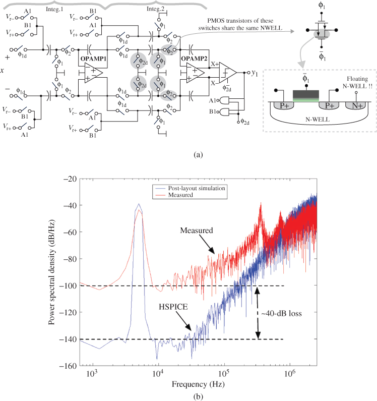
In conclusion, the layout phase of ![]() Ms is a critical stage of the design procedure and it must be carefully verified and checked using verification CAD tools without underestimating any warning message or apparently minor issue, which may become the cause of a catastrophic failure.
Ms is a critical stage of the design procedure and it must be carefully verified and checked using verification CAD tools without underestimating any warning message or apparently minor issue, which may become the cause of a catastrophic failure.
4.7 Chip Package, Test PCB, and Experimental Set-Up
The last stage of the design phase of ![]() Ms deals with a number of tasks required to prepare the chip for testing its performance experimentally in a laboratory. The most important and critical considerations to take into account are the bonding diagram and chip package, the test PCB, and the experimental set-up. Some of these issues must be addressed before sending the chip for fabrication. This section describes the most important practical issues to be considered regarding packaging, prototyping, and testing of
Ms deals with a number of tasks required to prepare the chip for testing its performance experimentally in a laboratory. The most important and critical considerations to take into account are the bonding diagram and chip package, the test PCB, and the experimental set-up. Some of these issues must be addressed before sending the chip for fabrication. This section describes the most important practical issues to be considered regarding packaging, prototyping, and testing of ![]() Ms, assuming that they are going to be measured as stand-alone ICs. Similar recommendations can be followed in case the
Ms, assuming that they are going to be measured as stand-alone ICs. Similar recommendations can be followed in case the ![]() M is embedded in a system-on-chip (SoC) implementation.
M is embedded in a system-on-chip (SoC) implementation.
4.7.1 Bonding Diagram and Package
The bonding of the modulator chip has to be deeply analyzed, concerning the pad-ring placement described in previous section, the number of pads and pins assigned to supplies, guard rings, reference voltages, etc. Therefore, the selection of the most suitable chip package is a critical issue because the parasitics associated with the package and with its bonding connections to the chip may severely affect the performance of the modulator, particularly when high speed and/or high resolution are demanded.
Indeed, the effect of package and bonding-wire parasitics can be analyzed in detail by using dedicated CAD tools (such as Cadence Allegro), which allow to simulate the circuit considering these parasitic effects. Some tools, such as Cadence PKG, allow modeling of the package by an equivalent LCR circuit that is synthesized from the physical and electrical characteristics of a given package. Among others, the most important limitations come from the parasitic bonding inductances. It is recommendable to use surface-mount devices (SMDs) such as ball grid array (BGA) or quad flat package (QFP)—the latter being quite commonly used for testing ASIC prototypes in general and ![]() ICs in particular.
ICs in particular.
Some critical considerations must be also taken into account. On the one hand, bonding pads of the same type (analog, mixed-signal, digital, or digital I/Os) must be placed together and apart from the rest using power-cut diode cells similar to those shown in Figure 4.76. This allows power separation and avoids cross-talk. Moreover, supply pads and pins should be placed in parallel to reduce the total parasitic inductance due to the compensation given by the complementary mutual inductances [44]. On the other hand, double-bonding techniques and multiple pins are frequently used for the supplies of the different sections in order to reduce the inductance of the paths to the chip and decrease supply bounce. Note that if reference voltages are provided externally (off-chip), double bonding should be also used for the reference pads/pins in order to halve their bonding parasitic inductances as well.
4.7.2 Test PCB
In order to characterize the ![]() M IC, a special-purpose PCB is needed in order to connect the chip to the different test instruments providing the necessary signals, biasing, and supply voltages, as well as to capture the modulator output data for further processing in a computer. Owing to the aforementioned practical limitations associated with the chip packages, other testing approaches are considered, particularly in very high-speed applications. For instance, the modulator die can be directly bonded to the test PCB, without using any package, in order to reduce the dimensions of bonding and consequently the parasitic inductances [9]. Alternatively, low-temperature co-fired ceramic (LTCC) substrates—commonly used in RF applications—can be used for reducing the effect of off-chip circuit element parasitics, as these elements can be embedded together with the modulator die into the same ceramic package.
M IC, a special-purpose PCB is needed in order to connect the chip to the different test instruments providing the necessary signals, biasing, and supply voltages, as well as to capture the modulator output data for further processing in a computer. Owing to the aforementioned practical limitations associated with the chip packages, other testing approaches are considered, particularly in very high-speed applications. For instance, the modulator die can be directly bonded to the test PCB, without using any package, in order to reduce the dimensions of bonding and consequently the parasitic inductances [9]. Alternatively, low-temperature co-fired ceramic (LTCC) substrates—commonly used in RF applications—can be used for reducing the effect of off-chip circuit element parasitics, as these elements can be embedded together with the modulator die into the same ceramic package.
Let us consider the most common approach that consists of a chip package connected to the necessary circuits for testing in a multilayer PCB. Figure 4.79 shows the conceptual schematic of a PCB used for testing the ![]() M of Figure 4.75 [50]. In this example, a 32-pin QFP package is used. Note that, in addition to the effect of circuit parasitics themselves, external electromagnetic interferences are injected into the
M of Figure 4.75 [50]. In this example, a 32-pin QFP package is used. Note that, in addition to the effect of circuit parasitics themselves, external electromagnetic interferences are injected into the ![]() M chip through both inductive and capacitive coupling. In order to reduce the impact of off-chip circuit parasitics and to obtain a robust test circuit, the following circuit strategies are usually incorporated in the test PCB (some of them highlighted in Figure 4.79):
M chip through both inductive and capacitive coupling. In order to reduce the impact of off-chip circuit parasitics and to obtain a robust test circuit, the following circuit strategies are usually incorporated in the test PCB (some of them highlighted in Figure 4.79):
- Separate the PCB into different areas or planes corresponding to the analog, mixed-signal, and digital signals. Ground planes should be separated—usually with a gap larger than 1/8—and connected only in one point. This way noisy return currents are minimized.
- Use regulators to keep the values of the supply voltages stable.
- Use decoupling capacitors in the supply, biasing, and reference voltage lines. It is a common practice to combine a large tantalum capacitor with a small ceramic capacitor connected in parallel, in such a way that the ceramic capacitor is placed as close as to the package pin. Both capacitors are usually connected together with one inductor in a
 -filter configuration, as illustrated in Figure 4.79.
 - Keep digital signal paths as far as possible from the sensitive analog pins.
- Use termination resistors for impedance coupling in the digital output lines.
- Use ESD protection diodes for sensitive input pins, particularly if they are not used in the corresponding bonding pads.
Figure 4.79 Conceptual schematic of a test PCB used for measuring the performance of the modulator in Figure 4.75. Note that this is a simplified version of the modulator presented in [50], which included a programmable-gain front-end integrator and a preamplifier connected to the modulator. The additional pins required to include these circuits have been omitted for the sake of simplicity. Moreover, the values of circuit elements in this test chip correspond to the signal specifications reported in [50]: ![]() kHz and DR
kHz and DR ![]() dB.
dB.
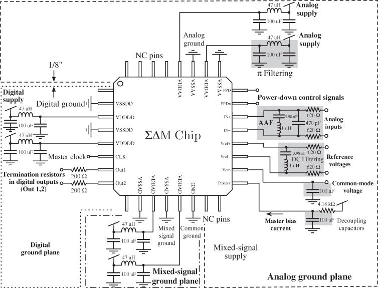
Apart from the aforementioned techniques, PCBs used for testing ![]() Ms should contain an AAF. A low-order (typically first- or second-order) RC filter is enough in the majority of practical situations.
Ms should contain an AAF. A low-order (typically first- or second-order) RC filter is enough in the majority of practical situations.
4.7.3 Experimental Test Set-Up
The test set-up and instruments used for measuring the performance of ![]() Ms in the laboratory are also very important and need to be carefully planned. The number and type of laboratory equipment depend on different factors including the nature of the signal to be tested (low-pass, band-pass, sinewave, modulated signal, etc.), the target modulator specifications (in-band noise power, linearity, etc.), the type of performance metrics to be measured (output spectrum, SNR/SNDR, HD3, IM3, INL, etc.), and so forth.
Ms in the laboratory are also very important and need to be carefully planned. The number and type of laboratory equipment depend on different factors including the nature of the signal to be tested (low-pass, band-pass, sinewave, modulated signal, etc.), the target modulator specifications (in-band noise power, linearity, etc.), the type of performance metrics to be measured (output spectrum, SNR/SNDR, HD3, IM3, INL, etc.), and so forth.
Planning the Types and Number of Equipment Needed
It should be noted, however, that every additional circuit element or laboratory instrument included in the measurement set-up is a potential source of errors and interference that may degrade the modulator performance. For that reason, it is very important to think in advance—preferably during the design phase—of the kind of measurements that will be needed and the type and number of instruments which will be required. In many practical situations, the performance of the chip cannot be properly characterized experimentally because of limitations imposed by the lab equipment and instruments. Some examples of these limitations are the jitter error of the clock generators, the maximum frequency/linearity provided by the signal generator, the maximum capture rate of the logic analyzer, etc.
Generally speaking, regardless of the specific measurements to be carried out, at least the following instruments are commonly needed for testing ![]() Ms:
Ms:
- Power supply generators to generate the supply voltages, reference voltages, common-mode voltage as well as any other DC voltage or bias current required. Whenever possible, it is highly recommended to use a voltage regulator circuit—embedded in the test PCB—to generate all DC and bias signals from a single voltage supply to minimize the number of instruments and wires.
- Analog (input) signal generators, at least one sinewave generator, if possible providing balanced fully-differential signals with the required bandwidth and accuracy—in terms of noise and linearity. Note that the same common-mode voltage generator must be used for both the signal generator and the modulator chip. Otherwise, a systematic offset will be introduced at the modulator inputs, which may severely degrade the performance of the modulator.
- Clock generator with the required performance in terms of frequency, logic levels, and clock jitter error.
- Data acquisition systems, such as logic analyzers or SoC test units (for instance, Agilent 93000), are essential for capturing the modulator output bitstreams, which are transferred to a personal computer or to a workstation in order to process the data.21
As mentioned previously, apart from the “essential” instruments, other laboratory equipment may eventually be needed, such as spectrum analyzers to check the frequency spectrum of a given signal “on the fly,” multimeters to measure the DC operating point, etc.
Connecting Laboratory Instruments
The connection of the different instruments to the test PCB is critical, and must be implemented in such a way that their parasitics are minimized. Among others, the following recommendations must be followed:
- Use the appropriate connectors for each instrument in the PCB, as illustrated in Figure 4.80.
- Reduce the length and number of cables used for connecting the instruments.
- Make sure that the ground of each instrument is connected to its corresponding ground in the PCB, that is, instruments providing analog signals should have their grounds connected to the analog ground in the PCB.
- Make sure that all grounds are connected in star configuration as conceptually depicted in Figure 4.81a. Do not use the scheme shown in Figure 4.81b, where the ground of one instrument is connected to the ground of another instrument and so on.
Figure 4.80 Illustrating some connectors of different instruments in a ![]() M IC test PCB.
M IC test PCB.

Figure 4.81 Illustrating the ground connection of different laboratory instruments to the test PCB.

Last but not least, another important issue to take into account in the set-up deals with turn-on/off sequence followed to switch on/off the different instruments involved. Thus, the turn-on sequence should start with the supply voltage, followed by the clock-signal generator, and finally, the analog signal generator. The turn-off sequence should be carried out in the opposite way.
Measurement Set-Up Example
Figure 4.82 shows the conceptual diagram of a measurement set-up based on a logic analyzer as the data acquisition system [9]. In this case, an Agilent A3631A unit generates the voltage supply, whereas the fully-differential input signal is generated by a Tektronix SG5010 audio oscillator. An optional SRS CG635 clock generator can be used for generating the clock signal, whereas an Agilent A16823B logic analyzer22 is used for acquiring the modulator output bitstreams and also for generating the digital control signals required to test the modulator. After bitstream acquisition, data is post-processed in MATLAB. Note that, in the case of cascade modulators in which the DCL is not implemented on-chip, a procedure similar to that described in Section 4.3 can be followed to process the output results.
Figure 4.82 Conceptual example of a ![]() M measurement set-up based on a logic analyzer.
M measurement set-up based on a logic analyzer.
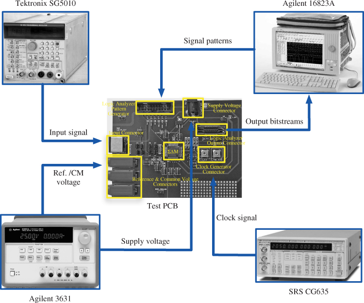
4.8 Summary
This chapter presented a design guide that includes a collection of practical recipes to be taken into account in the electrical design and characterization of ![]() Ms, going from macromodel representation of their building blocks to their transistor-level and physical-level implementation, including layout, packaging, and test set-up. A complete description of the macromodels frequently used for the main building blocks has been presented, giving some examples on how to use them in both SC and CT-
Ms, going from macromodel representation of their building blocks to their transistor-level and physical-level implementation, including layout, packaging, and test set-up. A complete description of the macromodels frequently used for the main building blocks has been presented, giving some examples on how to use them in both SC and CT-![]() Ms. At the transistor level, the most important design considerations of
Ms. At the transistor level, the most important design considerations of ![]() M circuit blocks have been detailed, including amplifiers, transconductors, switches, comparators, and DACs. Several design examples and simulation test benches have been illustrated, emphasizing on their implementation in Cadence Design FrameWork II. Apart from the building-block design itself, a number of practical issues related to the electrical characterization of
M circuit blocks have been detailed, including amplifiers, transconductors, switches, comparators, and DACs. Several design examples and simulation test benches have been illustrated, emphasizing on their implementation in Cadence Design FrameWork II. Apart from the building-block design itself, a number of practical issues related to the electrical characterization of ![]() Ms, such as the injection of noise sources in transient electrical simulations and the post-processing of simulation results, have been also addressed.
Ms, such as the injection of noise sources in transient electrical simulations and the post-processing of simulation results, have been also addressed.
The diverse aspects covered in this chapter close the design flow of ![]() Ms discussed in this book, going from ideal fundamentals and architecture considerations given in Chapter 1, to the impact of nonideal errors at system level discussed in Chapter 2, and to their application to the high-level synthesis and verification using behavioral models and simulation, which is detailed in Chapter 3. This systematic top-down/bottom-up design methodology is complemented in Chapter 5 with an exhaustive study of the state-of-the-art on
Ms discussed in this book, going from ideal fundamentals and architecture considerations given in Chapter 1, to the impact of nonideal errors at system level discussed in Chapter 2, and to their application to the high-level synthesis and verification using behavioral models and simulation, which is detailed in Chapter 3. This systematic top-down/bottom-up design methodology is complemented in Chapter 5 with an exhaustive study of the state-of-the-art on ![]() Ms in order to help designers select the optimum
Ms in order to help designers select the optimum ![]() M architecture and circuit technique for their applications together with identifying the trends, challenges, and practical solutions which have been proposed in each case by the
M architecture and circuit technique for their applications together with identifying the trends, challenges, and practical solutions which have been proposed in each case by the ![]() M design community.
M design community.
References
[1] K. Kundert and O. Zinke, The Designer's Guide to Verilog-AMS, Kluwer Academic Publishers, 2004.
[2] G. Suárez, M. Jiménez, and F. O. Fernández, “Behavioral Modeling Methods for Switched-Capacitor ![]() Modulators,” IEEE Transactions on Circuits and Systems - I: Regular Papers, vol. 54, pp. 1236–1244, June 2007.
Modulators,” IEEE Transactions on Circuits and Systems - I: Regular Papers, vol. 54, pp. 1236–1244, June 2007.
[3] J. M. Rabaey, SPICE 3 User Guide. [Online]. Available: http://bwrc.eecs.berkeley.edu/classes/icbook/ spice/.
[4] A. Vladimirescu, The SPICE Book. John Wiley & Sons, 1994.
[5] Y. Tsividis, “Integrated Continuous-Time Filter Design—An Overview,” IEEE Journal of Solid-State Circuits, vol. 29, pp. 166–176, March 1994.
[6] S. Pavan, “Efficient Simulation of Weak Nonlinearities in Continuous Time Oversampling Converters,” IEEE Transactions on Circuits and Systems I—Regular Papers, vol. 57, pp. 1925–1934, August 2010.
[7] B. Razavi, Principles of Data Conversion System Design, IEEE Press, 1995.
[8] F. Maloberti, Data Converters, Springer, 2007.
[9] A. Morgado, R. del Río, and J. M. de la Rosa, Nanometer CMOS Sigma-Delta Modulators for Software Defined Radio, Springer, 2011.
[10] Verilog-A. Language Reference Manual: Analog Extensions to Verilog HDL, Open Verilog International, 1996.
[11] Cadence Verilog-A Language Reference, Cadence Design Systems Inc., 2006.
[12] J. Gonzálex and E. Alarcón, “Current-Steering High-Speed D/A Converters for Communications,” Chapter 3 in CMOS Telecom Data Converters (A. Rodríguez-Vázquez, F. Medeiro, and E. Janssens, Editors), Kluwer Academic Publishers, 2003.
[13] M. Ortmanns and F. Gerfers, Continuous-Time Sigma-Delta A/D Conversion: Fundamentals, Performance Limits and Robust Implementations, Springer, 2006.
[14] J. M. de la Rosa, B. Pérez-Verdú, and A. Rodríguez-Vázquez, Systematic Design of CMOS Switched-Current Bandpass Sigma-Delta Modulators for Digital Communication Chips, Kluwer Academic Publishers, 2002.
[15] Virtuoso® Spectre® Circuit Simulator User Guide, Cadence Design Systems Inc., 2010.
[16] The HSPICE Documentation Set, Synopsys Inc., 2005.
[17] W. Bennett, “Spectra of Quantized Signals,” Bell System Technical Journal, vol. 27, pp. 446–472, July 1948.
[18] F. Medeiro, B. Pérez-Verdú, and A. Rodríguez-Vázquez, Top-Down Design of High-Performance Sigma-Delta Modulators, Kluwer Academic Publishers, 1999.
[19] Y. Dong and A. Opal, “Time-Domain Thermal Noise Simulation of Switched Capacitor Circuits and Delta-Sigma Modulators,” IEEE Transactions on Computer Aided Design of Integrated Circuits and Systems, vol. 19, pp. 473–481, April 2000.
[20] J. Kasdin, “Discrete Simulation of Colored Noise and Stochastic Processes and ![]() : Power Law Noise Generation,” Proceedings of the IEEE, vol. 83, pp. 802–827, February 1995.
: Power Law Noise Generation,” Proceedings of the IEEE, vol. 83, pp. 802–827, February 1995.
[21] Virtuoso® Schematic Editor L User Guide, Cadence Design Systems Inc., 2008.
[22] R. del Río, F. Medeiro, B. Pérez-Verdú, J. M. de la Rosa, and A. Rodríguez-Vázquez, CMOS Cascade ![]() Modulators for Sensors and Telecom: Error Analysis and Practical Design, Springer, 2006.
Modulators for Sensors and Telecom: Error Analysis and Practical Design, Springer, 2006.
[23] Y. Geerts, M. Steyaert, and W. Sansen, Design of Multi-bit Delta-Sigma A/D Converters, Kluwer Academic Publishers, 2002.
[24] S. Narayanan, “Application of Volterra Series to Intermodulation Distortion of Transistor Feedback Amplifier,” IEEE Transactions Circuit Theory, pp. 518–527, November 1970.
[25] P. Wambacq, G. Gielen, P. Kinget, and W. Sansen, “High-Frequency Distortion Analysis of Analog Integrated Circuits,” IEEE Transactions on Circuits and Systems—II: Analog and Digital Signal Processing, vol. 46, pp. 335–345, March 1999.
[26] W. Yu, S. Sen, and B. Leung, “Distortion Analysis of MOS Track-and-hold Sampling Mixers Using Time-varying Volterra Series,” IEEE Transactions on Circuits and Systems—II: Analog and Digital Signal Processing, vol. 46, pp. 101–113, February 1999.
[27] R. Schreier and G. C. Temes, Understanding Delta-Sigma Data Converters, IEEE Press, 2005.
[28] A. Morgado, R. del Río, J. M. de la Rosa, R. Castro-López, and B. Pérez-Verdú, “A 0.13 ![]() m CMOS Adaptive Sigma-Delta Modulator for Triple-Mode GSM/Bluetooth/UMTS Applications,” Microelectronics Journal, vol. 41, pp. 277–290, 2010.
m CMOS Adaptive Sigma-Delta Modulator for Triple-Mode GSM/Bluetooth/UMTS Applications,” Microelectronics Journal, vol. 41, pp. 277–290, 2010.
[29] R. Tortosa, A. Aceituno, J. M. de la Rosa, A. Rodríguez-Vázquez, and F. V. Fernández, “A 12-bit, 40MS/s Gm-C Cascade 3-2 Continuous-Time Sigma-Delta Modulator,” Proc. of the IEEE Intl. Symp. on Circuits and Systems, pp. 1–4, 2007.
[30] P. Allen and D. Holberg, CMOS Analog Circuit Design, 2nd edn, Oxford University Press, 2002.
[31] A. Rodríguez-Vázquez et al., “Comparator Circuits,” Wiley Encyclopedia of Electrical and Electronics Engineering, pp. 577–600, John Wiley & Sons, 1999.
[32] B. Nikoli et al., “Improved Sense-Amplifier-Based Flip-Flop: Design and Measurements,” IEEE Journal of Solid-State Circuits, vol. 35, pp. 876–884, June 2000.
[33] T. Kobayashi et al., “A Current-Controlled Latch Sense Amplifier and a Static Power-Saving Input Buffer for Low-Power Architecture,” IEEE Journal of Solid-State Circuits, vol. 28, pp. 523–527, April 1993.
[34] A. Yukawa, “A CMOS 8-bit High-Speed Converter IC,” IEEE Journal of Solid-State Circuits, vol. 20, pp. 775–779, June 1985.
[35] Y. Wang and B. Razavi, “An 8-Bit 150-MHz CMOS A/D Converter,” IEEE Journal of Solid-State Circuits, vol. 35, pp. 308–317, March 2000.
[36] G. Yin et al., “A High-Speed CMOS Comparator with 8-b Resolution,” IEEE Journal of Solid-State Circuits, vol. 27, pp. 208–211, February 1992.
[37] W. Press et al., Numerical Recipes in C. The Art of Scientific Computing, 2nd edn, Cambridge University Press, 1992.
[38] S. Yan and E. Sánchez-Sinencio, “A Continuous-Time ![]() Modulator With 88-dB Dynamic Range and 1.1-MHz Signal Bandwidth,” IEEE Journal of Solid-State Circuits, vol. 39, pp. 75–86, January 2004.
Modulator With 88-dB Dynamic Range and 1.1-MHz Signal Bandwidth,” IEEE Journal of Solid-State Circuits, vol. 39, pp. 75–86, January 2004.
[39] P. Crombez et al., “A Single-Bit 500 kHz-10 MHz Multimode Power-Performance Scalable 83-to-67 dB DR CT ![]() Modulator for SDR in 90 nm Digital CMOS,” IEEE Journal of Solid-State Circuits, vol. 45, pp. 1159–1171, June 2010.
Modulator for SDR in 90 nm Digital CMOS,” IEEE Journal of Solid-State Circuits, vol. 45, pp. 1159–1171, June 2010.
[40] L. Breems, R. Rutten, and G. Wetzker, “A Cascaded Continuous-Time ![]() Modulator with 67-dB Dynamic Range in 10-MHz Bandwidth,” IEEE Journal of Solid-State Circuits, vol. 39, pp. 2152–2160, December 2004.
Modulator with 67-dB Dynamic Range in 10-MHz Bandwidth,” IEEE Journal of Solid-State Circuits, vol. 39, pp. 2152–2160, December 2004.
[41] G. Mitteregger, C. Ebner, S. Mechnig, T. Blon, C. Holuigue, and E. Romani, “A 20-mW 640-MHz CMOS Continuous-Time ![]() ADC With 20-MHz Signal Bandwidth, 80-dB Dynamic Range and 12-bit ENOB,” IEEE Journal of Solid-State Circuits, vol. 41, pp. 2641–2649, December 2006.
ADC With 20-MHz Signal Bandwidth, 80-dB Dynamic Range and 12-bit ENOB,” IEEE Journal of Solid-State Circuits, vol. 41, pp. 2641–2649, December 2006.
[42] M. Bolatkale et al., “A 4GHz Continuous-Time ![]() ADC With 70dB DR and –74 dBFS THD in 125 MHz BW,” IEEE Journal of Solid-State Circuits, vol. 46, pp. 2857–2868, December 2011.
ADC With 70dB DR and –74 dBFS THD in 125 MHz BW,” IEEE Journal of Solid-State Circuits, vol. 46, pp. 2857–2868, December 2011.
[43] K. Lee and R. Meyer, “A Current-Controlled Latch Sense Amplifier and a Static Power-Saving Input Buffer for Low-Power Architecture,” IEEE Journal of Solid-State Circuits, vol. 20, pp. 1103–1113, December 1985.
[44] B. Razavi, Design of Analog CMOS Integrated Circuits, McGraw-Hill, 2000.
[45] A. Morgado, R. del Río, J. M. de la Rosa, L. Bos, J. Ryckaert, and G. van der Plas, “A 100kHz-10MHz BW, 78-to-52dB DR,4.6-to-11mW Flexible SC ![]() Modulator in 1.2-V 90-nm CMOS,” Proc. of the IEEE European Solid-State Circuits Conf., pp. 418–421, September 2010.
Modulator in 1.2-V 90-nm CMOS,” Proc. of the IEEE European Solid-State Circuits Conf., pp. 418–421, September 2010.
[46] M. Felder and J. Ganger, “Analysis of Ground-Bounce Induced Substrate Noise Coupling in a Low Resistive Bulk Epitaxial Process: Design Strategies to Minimize Noise Effects on a Mixed-Signal Chip,” IEEE Transactions on Circuits and Systems—II: Analog and Digital Signal Processing, vol. 46, pp. 1427–1436, October 1999.
[47] F. Maloberti, “Layout of Analog and Mixed Analog-Digital Circuits,” Chapter 11 in Design of Analog-Digital VLSI Circuits for Telecommunications and Signal Processing (J. Franca and Y. Tsividis, Editors), Prentice-Hall, 1994.
[48] Y. Tsividis, Mixed Analog-Digital VLSI Devices and Technology: An Introduction, McGraw-Hill, 1996.
[49] S. Cao et al., “ESD Design Strategies for High-Speed Digital and RF Circuits in Deeply Scaled Silicon Technologies,” IEEE Transactions on Circuits and Systems—I: Regular Papers, vol. 57, pp. 2301–2311, September 2010.
[50] J. M. de la Rosa et al., “A CMOS 110-dB@40-kS/s Programmable-Gain Chopper-Stabilized Third-Order 2-1 Cascade Sigma-Delta Modulator for Low-Power High-Linearity Automotive Sensor ASICs,” IEEE Journal of Solid-State Circuits, vol. 40, pp. 2246–2264, November 2005.
1 Note that quasi ideal values of ![]() and
and ![]() can cause tolerance and convergence problems in electrical simulations. This can be controlled by properly setting the corresponding numerical tolerance parameters in the simulation options [4].
can cause tolerance and convergence problems in electrical simulations. This can be controlled by properly setting the corresponding numerical tolerance parameters in the simulation options [4].
2 These resistors are commonly implemented in practice using unsalicided ![]() poly layers [9].
poly layers [9].
3 Current-mode feedback DACs are also used in SI-![]() Ms, which are a particular case of DT-
Ms, which are a particular case of DT-![]() Ms where the loop filter processes current-mode signals, and it is implemented with SI integrators instead of SC integrators [14]. The difference between switched-current cells and current-steering DACs will be discussed later on in this chapter.
Ms where the loop filter processes current-mode signals, and it is implemented with SI integrators instead of SC integrators [14]. The difference between switched-current cells and current-steering DACs will be discussed later on in this chapter.
4 Alternatively, a more ideal macromodel can be simply based on voltage-controlled current sources as will be illustrated later in this chapter.
5 The majority of examples included in this book used Synopsis® HSPICE®. However, recent versions of some SPICE-like simulators, such as Cadence-Spectre [15] incorporates the possibility to include noise sources in transient analysis. However, the method described in this section allows to isolate the effect of a given noise source instead of considering all noise sources acting together, as done in a regular noise analysis in CADENCE-SPECTRE. Moreover, the methodology explained in this book is well known and can be applied to the majority of SPICE-like simulators, including SPECTRE as well.
6 The procedure described in this section can be applied to the experimental output results measured in the laboratory, discussed later in this chapter.
7 Some subcircuits, such as some types of SC common-mode feedback (CMFB) circuits or the latches used in some comparators, may use either nMOS or pMOS switches. However, the vast majority of switches in SC-![]() Ms are implemented as CMOS transmission gates.
Ms are implemented as CMOS transmission gates.
8 The input sinewave frequency ![]() should be located precisely in an FFT bin in order to avoid signal power to spread to adjacent bins [27]. To this end, the number of periods
should be located precisely in an FFT bin in order to avoid signal power to spread to adjacent bins [27]. To this end, the number of periods ![]() of the input signal within the simulated time (
of the input signal within the simulated time (![]() , where
, where ![]() stands for the number of points in the FFT and
stands for the number of points in the FFT and ![]() for the sampling frequency) must be an integer. To meet this constraint, the value of the input frequency can thus be adjusted according to
for the sampling frequency) must be an integer. To meet this constraint, the value of the input frequency can thus be adjusted according to
9 Note that the measured values for ![]() and GB, and the loading capacitor
and GB, and the loading capacitor ![]() , can be combined to provide an estimation of the amplifier output parasitic capacitor
, can be combined to provide an estimation of the amplifier output parasitic capacitor ![]() . Given that
. Given that ![]() in a single-stage amplifier,
in a single-stage amplifier, ![]() for the folded cascode amplifier under consideration.
for the folded cascode amplifier under consideration.
10 Strobe phase is the clock phase in which the comparator is active, that is, it is comparing the input signals. This phase is sometimes referred to as amplification phase or simply comparison phase.
11 Some comparators used in SC-![]() Ms with feed-forward paths include an SC network at the input of the preamplifier to merge with SC adders. These SC networks may be used also for improving the preamplifier performance and for implementing reconfiguration of the number of bits of the embedded quantizer [9].
Ms with feed-forward paths include an SC network at the input of the preamplifier to merge with SC adders. These SC networks may be used also for improving the preamplifier performance and for implementing reconfiguration of the number of bits of the embedded quantizer [9].
12 The SR flip-flop is a digital circuit that in the majority of cases can be designed using minimum sizes.
13 The difference between SI and CS techniques is discussed later.
14 As will be discussed later, the high impedance output node of a Gm-C transconductor may be not suited to inject the feedback current provided by a CS DAC because of two main reasons. On the one hand, large signal swings reduce the voltage headroom required to keep the current cell transistors in the saturation region. On the other hand, the high impedance node causes that small current errors result in large voltage errors on the capacitors.
15 Design considerations of switches described in Section 4.4.1 must also be taken into account. In most practical cases, simple nMOS/pMOS switches satisfy the required specifications of CS DACs.
16 One of the main disadvantages of using soft-driving techniques is that an additional level-shifter circuit is required to generate the switch control voltages.
17 Some CT-![]() Ms using clock signals in the gigahertz range use off-chip ultra-low-jitter signal sources and
Ms using clock signals in the gigahertz range use off-chip ultra-low-jitter signal sources and ![]() -hybrid circuits to generate the master clock and its complementary signal [42].
-hybrid circuits to generate the master clock and its complementary signal [42].
18 In a design prototype, ![]() M reference voltages can be optionally provided by an off-chip circuit included in a test PCB as will be discussed later. However, this solution is neither practical nor robust if the
M reference voltages can be optionally provided by an off-chip circuit included in a test PCB as will be discussed later. However, this solution is neither practical nor robust if the ![]() M is embedded in a chip together with other circuit components which form a given electronic system.
M is embedded in a chip together with other circuit components which form a given electronic system.
19 If single-finger transistors are used, the analog signals can be directly routed to the transistor diffusions, while the digital signals can be connected to the transistor gate either using polysilicon or metal layers.
20 Many times, industrial partners working in a given project are interested in testing high-performance analog cells such as ![]() Ms in a cutting-edge technology.
Ms in a cutting-edge technology.
21 Many logic analyzers at present have an embedded PC, so that the same instrument is used for capturing the ![]() M output data and for processing this data, for instance, using MATLAB. Alternatively, some logic analyzers and SoC test units can be also used for generating the input signal waveforms, supply voltages, digital control signals, etc.
M output data and for processing this data, for instance, using MATLAB. Alternatively, some logic analyzers and SoC test units can be also used for generating the input signal waveforms, supply voltages, digital control signals, etc.
22 Depending on the electrical characteristics demanded for the clock signal, particularly the jitter error specification, it can be generated by a logic analyzer. If a very low-jitter clock signal is required, then an appropriate clock-signal generator should be used instead.