
CHAPTER 4 RF/IF Circuits
Chapter Introduction
From cellular phones to two-way pagers to wireless Internet access, the world is becoming more connected, even though wirelessly. No matter the technology, these devices are basically simple radio transceivers (transmitters and receivers). In the vast majority of cases the receivers and transmitters are a variation on the superheterodyne radio shown in Figure 4-1 for the receiver and Figure 4-2 for the transmitter.


The basic concept of operation is as follows. For the receiver, the signal from the antenna is amplified in the radio frequency (RF) stage. The output of the RF stage is one input of a mixer. A local oscillator (LO) is the other input. The output of the mixer is at the intermediate frequency (IF). The concept here is that it is much easier to build a high gain amplifier string at a narrow frequency band than it is to build a wideband, high gain amplifier. Also, the modulation bandwidth is typically very much smaller than the carrier frequency. A second mixer stage converts the signal to the baseband. The signal is then demodulated (demod). The modulation technique is independent from the receiver technology. The modulation scheme could be amplitude modulation (AM), frequency modulation (FM), phase modulation, or some form of quadrature amplitude modulation (QAM), which is a combination of amplitude and phase modulation.
To put some numbers around it, let us consider a broadcast FM signal. The carrier frequency is in the range of 98–108 MHz. The IF frequency is almost always 10.7 MHz. The baseband is 0 Hz–15 kHz. This is the sum of the right and left audio frequencies. There is also a modulation band centered at 38 kHz that is the difference of the left and right audio signals. This difference signal is demodulated and summed with the sum signal to generate the separate left and right audio signals.
On the transmit side the mixers convert the frequencies up instead of down.
These simplified block diagrams neglect some of the refinements that may be incorporated into these designs, such as power monitoring and control of the transmitter power amplifier as achieved with the “Tru-Power” circuits.
As technology has improved, we have seen the proliferation of IF sampling. Analog-to-digital converters (ADCs) of sufficient performance have been developed which allow the sampling of the signal at the IF frequency range, with demodulation occurring in the digital domain. This allows for system simplification by eliminating a mixer stage.
In addition to the basic building blocks that are the subject of this chapter, these circuit blocks often appear as building blocks in larger application specific integrated circuits (ASIC).
SECTION 4-1 Mixers
The Ideal Mixer
An idealized mixer is shown in Figure 4-3. An RF (or IF) mixer (not to be confused with video and audio mixers) is an active or passive device that converts a signal from one frequency to another. It can either modulate or demodulate a signal. It has three signal connections, which are called ports in the language of radio engineers. These three ports are the RF input, the LO input, and the IF output.

A mixer takes an RF input signal at a frequency fRF, mixes it with a LO signal at a frequency fLO, and produces an IF output signal that consists of the sum and difference frequencies, fRF ± fLO. The user provides a bandpass filter that follows the mixer and selects the sum (fRF + fLO) or difference (fRF −fLO) frequency.
Some points to note about mixers and their terminology:
• When the sum frequency is used as the IF, the mixer is called an upconverter; when the difference is used, the mixer is called a downconverter. The former is typically used in a transmit channel; the latter in a receive channel.
• In a receiver, when the LO frequency is below the RF, it is called low side injection and the mixer a low side downconverter; when the LO is above the RF, it is called high side injection, and the mixer a high side downconverter.
• Each of the outputs is only half the amplitude (one-quarter the power) of the individual inputs; thus, there is a loss of 6 dB in this ideal linear mixer. (In a practical multiplier, the conversion loss may be greater than 6 dB, depending on the scaling parameters of the device. Here, we assume a mathematical multiplier, having no dimensional attributes).
A mixer can be implemented in several ways, using active or passive techniques.
Ideally, to meet the low noise, high linearity objectives of a mixer we need some circuit that implements a polarity-switching function in response to the LO input. Thus, the mixer can be reduced to Figure 4-4, which shows the RF signal being split into in-phase (0°) and antiphase (180°) components; a changeover switch, driven by the LO signal, alternately selects the in-phase and antiphase signals. Thus reduced to essentials, the ideal mixer can be modeled as a sign-switcher.

In a perfect embodiment, this mixer would have no noise (the switch would have zero resistance), no limit to the maximum signal amplitude, and would develop no intermodulation between the various RF signals. Although simple in concept, the waveform at the IF output can be very complex for even a small number of signals in the input spectrum. Figure 4-6 shows the result of mixing just a single input at 11 MHz with an LO of 10 MHz.

The wanted IF at the difference frequency of 1 MHz is still visible in this waveform, and the 21 MHz sum is also apparent. How are we to analyze this?
We still have a product, but now it is that of a sinusoid (the RF input) at ωRF and a variable that can only have the values +1 or −1, that is, a unit square wave at ωLO. The latter can be expressed as a Fourier series.
Thus, the output of the switching mixer is its RF input, which we can simplify as sin ωRFt, multiplied by the above expansion for the square wave, producing:
Now expanding each of the products, we obtain:
 (4-3)
(4-3)or simply
The most important of these harmonic components are sketched in Figure 4-5 for the particular case used to generate the waveform shown in Figure 4-6, that is, fRF = 11 MHz and fLO = 10 MHz. Because of the 2/π term, a mixer has a minimum 3.92 dB insertion loss (and noise figure) in the absence of any gain.

Note that the ideal (switching) mixer has exactly the same problem of image response to ωLO −ωRF as the linear multiplying mixer. The image response is somewhat subtle, as it does not immediately show up in the output spectrum: it is a latent response, awaiting the occurrence of the “wrong” frequency in the input spectrum.
Diode-Ring Mixer
For many years, the most common mixer topology for high performance applications has been the diodering mixer, one form of which is shown in Figure 4-7. The diodes, which may be silicon junction, silicon Schottky-barrier, or gallium–arsenide (GaAs) types, provide the essential switching action. We do not need to analyze this circuit in great detail, but note in passing that the LO drive needs to be quite high—often a substantial fraction of 1 W—in order to ensure that the diode conduction is strong enough to achieve low noise and to allow large signals to be converted without excessive spurious nonlinearity.
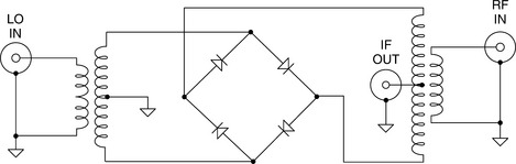
Because of the highly nonlinear nature of the diodes, the impedances at the three ports are poorly controlled, making matching difficult. Furthermore, there is considerable coupling between the three ports; this, and the high power needed at the LO port, make it very likely that there will be some component of the (highly distorted) LO signal coupled back toward the antenna. Finally, it will be apparent that a passive mixer such as this cannot provide conversion gain; in the idealized scenario, there will be a conversion loss of 2/π (as Eq. 4-4 shows), or 3.92 dB. A practical mixer will have higher losses, due to the resistances of the diodes and the losses in the transformers.
Users of this type of mixer are accustomed to judging the signal-handling capabilities by a “Level” rating. Thus, a Level-17 mixer needs +17 dBm (50 mW) of LO drive and can handle an RF input as high as + 10 dBm (± 1 V). A typical mixer in this class would be the Mini-Circuits LRMS-1H, covering 2–500 MHz, having a nominal insertion loss of 6.25 dB (8.5 dB maximum), a worst-case LO–RF isolation of 20 dB, and a worst-case LO–IF isolation of 22 dB (these figures for an LO frequency of 250–500 MHz). The price of this component is approximately $10.00 in small quantities. Even the most expensive diode-ring mixers have similar drive power requirements, high losses, and high coupling from the LO port.
The diode-ring mixer not only has certain performance limitations, but also is not amenable to fabrication using integrated circuit (IC) technologies, at least in the form shown in Figure 4-7. In the mid-1960s it was realized that the four diodes could be replaced by four transistors to perform essentially the same switching function. This formed the basis of the now-classical bipolar circuit shown in Figure 4-8, which is a minimal configuration for the fully balanced version. Millions of such mixers have been made, including variants in complementary-MOS (CMOS) and GaAs. We will limit our discussion to the bipolar junction transistor (BJT) form, an example of which is the Motorola MC1496, which, although quite rudimentary in structure, has been a mainstay in semi-discrete receiver designs for about 25 years.

The active mixer is attractive for the following reasons:
• It can be monolithically integrated with other signal processing circuitry.
• It can provide conversion gain, whereas a diode-ring mixer always has an insertion loss. (Note: active mixers may have gain. The Analog Devices’ AD831 active mixer, example, amplifies the result in Eq. 4-4 by π/2 to provide unity gain from RF to IF.)
• It requires much less power to drive the LO port.
• It provides excellent isolation between the signal ports.
• Is far less sensitive to load matching, requiring neither diplexer nor broadband termination.
Using appropriate design techniques it can provide tradeoffs between third-order intercept (3OI or IP3) and the 1 dB gain-compression point (P1dB), on the one hand, and total power consumption (PD) on the other. (That is, including the LO power, which in a passive mixer is “hidden” in the drive circuitry.)
Basic Operation of the Active Mixer
Unlike the diode-ring mixer, which performs the polarity-reversing switching function in the voltage domain, the active mixer performs the switching function in the current domain. Thus the active mixer core (transistors Q3–Q6 in Figure 4-8) must be driven by current-mode signals. The voltage-to-current converter formed by Q1 and Q2 receives the voltage-mode RF signal at their base terminals and transforms it into a differential pair of currents at their collectors.
A second point of difference between the active mixer and diode-ring mixer, therefore, is that the active mixer responds only to magnitude of the input voltage, not to the input power; that is, the active mixer is not matched to the source. (The concept of matching is that both the current and the voltage at some port are used by the circuitry which forms that port.) By altering the bias current, IEE, the transconductance of the input pair Q1–Q2 can be set over a wide range. Using this capability, an active mixer can provide variable gain.
A third point of difference is that the output (at the collectors of Q3–Q6) is in the form of a current, and can be converted back to a voltage at some other impedance level to that used at the input; hence, it can provide further gain. By combining both output currents (typically, using a transformer) this voltage gain can be doubled. Finally, it will be apparent that the isolation between the various ports, in particular, from the LO port to the RF port, is inherently much lower than can be achieved in the diode-ring mixer, due to the reversed-biased junctions that exist between the ports.
Briefly stated, though, the operation is as follows. In the absence of any voltage difference between the bases of Q1 and Q2, the collector currents of these two transistors are essentially equal. Thus, a voltage applied to the LO input results in no change of output current. Should a small DC offset voltage be present at the RF input (due typically to mismatch in the emitter areas of Q1 and Q2), this will only result in a small feedthrough of the LO signal to the IF output, which will be blocked by the first IF filter.
Conversely, if an RF signal is applied to the RF port, but no voltage difference is applied to the LO input, the output currents will again be balanced. A small offset voltage (due now to emitter mismatches in Q3–Q6) may cause some RF signal feedthrough to the IF output; as before, this will be rejected by the IF filters. It is only when a signal is applied to both the RF and LO ports that a signal appears at the output; hence, the term doubly balanced mixer.
Active mixers can realize their gain in one other way: the matching networks used to transform a 50 Ω source to the (usually) high input impedance of the mixer provide an impedance transformation and thus voltage gain due to the impedance step up. Thus, an active mixer that has loss when the input is terminated in a broadband 50 ω termination can have “gain” when an input matching network is used.
1 B. Gilbert, ISSCC Digest of Technical Papers 1968, February, 16, 1968, pp. 114–115.
2 Gilbert B. Journal of Solid State Circuits. 1968;Vol. SC-3:353–372. December
3 Ruthroff C.L. Some Broadband Transformers. Proceedings of the I.R.E. 1959;Vol. 47:1337–1342. August
4 J.M. Bryant, “Mixers for High Performance Radio,” Wescon 1981: Session 24, Electronic Conventions, Inc., Sepulveda Blvd., El Segundo, CA
5 P.E. Chadwick, “High Performance IC Mixers,” IERE Conference on Radio Receivers and Associated Systems, Leeds, 1981, IERE Conference Publication No. 50.
6 Chadwick P.E. Phase Noise, Intermodulation, and Dynamic Range January. CA: RF Expo, Anaheim, 1986.
SECTION 4-2 Modulators
Modulators (sometimes called balanced modulators, doubly balanced modulators, or even on occasions high level mixers) can be viewed as sign-changers. The two inputs, X and Y, generate an output W, which is simply one of these inputs (say, Y) multiplied by just the sign of the other (say, X), that is W = Y × sign(X). Therefore, no reference voltage is required. A good modulator exhibits very high linearity in its signal path, with precisely equal gain for positive and negative values of Y, and precisely equal gain for positive and negative values of X. Ideally, the amplitude of the X input needed to fully switch the output sign is very small; that is, the X-input exhibits a comparator-like behavior. In some cases, where this input may be a logic signal, a simpler X-channel can be used.
As an example, the AD8345 is a silicon RFIC quadrature modulator, designed for use from 250 to 1,000 MHz. Its excellent phase accuracy and amplitude balance enable the high performance direct modulation of an IF carrier (Figure 4-9).

The AD8345 accurately splits the external LO signal into two quadrature components through the polyphase phase-splitter network. The two I and Q LO components are mixed with the baseband I and Q differential input signals. Finally, the outputs of the two mixers are combined in the output stage to provide a single-ended 50 Ω drive at VOUT.
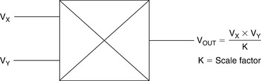
SECTION 4-3 Analog Multipliers
A multiplier is a device having two input ports and an output port. The signal at the output is the product of the two input signals. If both input and output signals are voltages, the transfer characteristic is the product of the two voltages divided by a scaling factor, K, which has the dimension of voltage (see Figure 4-10). From a mathematical point of view, multiplication is a “four-quadrant” operation—that is to say that both inputs may be either positive or negative and the output can be positive or negative (Figure 4-11). Some of the circuits used to produce electronic multipliers, however, are limited to signals of one polarity. If both signals must be unipolar, we have a “single-quadrant” multiplier, and the output will also be unipolar. If one of the signals is unipolar, but the other may have either polarity, the multiplier is a “two-quadrant” multiplier, and the output may have either polarity (and is “bipolar”). The circuitry used to produce one- and two-quadrant multipliers may be simpler than that required for four-quadrant multipliers, and since there are many applications where full four-quadrant multiplication is not required, it is common to find accurate devices which work only in one or two quadrants. An example is the AD539, a wideband dual two-quadrant multiplier which has a single unipolar VY input with a relatively limited bandwidth of 5 MHz, and two bipolar VX inputs, one per multiplier, with bandwidths of 60 MHz. A block diagram of the AD539 is shown in Figure 4-12.


The simplest electronic multipliers use logarithmic amplifiers. The computation relies on the fact that the antilog of the sum of the logs of two numbers is the product of those numbers (see Figure 4-13).

The disadvantages of this type of multiplication are the very limited bandwidth and single-quadrant operation. A far better type of multiplier uses the “Gilbert Cell.” This structure was invented by Barrie Gilbert, now of Analog Devices, in the late 1960s (see References 1 and 2).
There is a linear relationship between the collector current of a silicon junction transistor and its transconductance (gain) which is given by:
where IC is the collector current, VBE is the base–emitter voltage, q is the electron charge (1.60219 × 10⁻¹⁹), k is Boltzmann’s constant (1.38062 × 10⁻²³), and T is the absolute temperature.
This relationship may be exploited to construct a multiplier with a differential (long-tailed) pair of silicon transistors, as shown in Figure 4-14.

This is a rather poor multiplier because (1) the Y input is offset by the VBE which changes nonlinearly with VY; (2) the X input is nonlinear as a result of the exponential relationship between IC and VBE; and (3) the scale factor varies with temperature.
Gilbert realized that this circuit could be linearized and made temperature stable by working with currents, rather than voltages, and by exploiting the logarithmic IC/VBE properties of transistors (see Figure 4-15). The X input to the Gilbert Cell takes the form of a differential current, and the Y input is a unipolar current. The differential X currents flow in two diode-connected transistors, and the logarithmic voltages compensate for the exponential VBE/IC relationship. Furthermore, the q/kT scale factors cancel. This gives the Gilbert Cell the linear transfer function.

As it stands, the Gilbert Cell has three inconvenient features: (1) its X input is a differential current; (2) its output is a differential current; and (3) its Y input is a unipolar current—so the cell is only a two-quadrant multiplier.
By cross-coupling two such cells and using two voltage-to-current converters (as shown in Figure 4-16), we can convert the basic architecture to a four-quadrant device with voltage inputs, such as the AD534. At low and medium frequencies, a subtractor amplifier may be used to convert the differential current at the output to a voltage. Because of its voltage output architecture, the bandwidth of the AD534 is only about 1 MHz, although the AD734, a later version, has a bandwidth of 10 MHz.
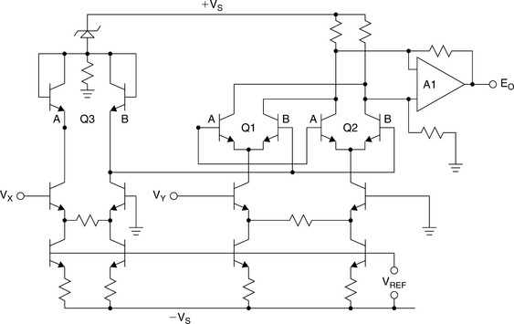
In Figure 4-16, Q1A and Q1B, and Q2A and Q2B form the two core long-tailed pairs of the two Gilbert Cells, while Q3A and Q3B are the linearizing transistors for both cells. In Figure 3-35 there is an operational amplifier acting as a differential current to single-ended voltage converter, but for higher speed applications, the cross-coupled collectors of Q1 and Q2 form a differential open collector current output (as in the AD834 500 MHz multiplier).
The translinear multiplier relies on the matching of a number of transistors and currents. This is easily accomplished on a monolithic chip. Even the best IC processes have some residual errors, however, and these show up as four DC error terms in such multipliers. Offset voltage on the X input shows up as feedthrough of the Y input. Conversely, offset voltage on the Y input shows up as feedthrough of the X input. Offset voltage on the Z input causes offset of the output signal, and resistor mismatch causes gain error. In early Gilbert Cell multipliers, these errors had to be trimmed by means of resistors and potentiometers external to the chip, which was somewhat inconvenient. With modern analog processes, which permit the laser trimming of SiCr thin film resistors on the chip itself, it is possible to trim these errors during manufacture so that the final device has very high accuracy. Internal trimming has the additional advantage that it does not reduce the high frequency performance, as may be the case with external trimpots.
Because the internal structure of the translinear multiplier is necessarily differential, the inputs are usually differential as well (after all, if a single-ended input is required it is not hard to ground one of the inputs). This is not only convenient in allowing common-mode signals to be rejected, it also permits more complex computations to be performed. The AD534 (shown previously in Figure 4-16) is the classic example of a four-quadrant multiplier based on the Gilbert Cell. It has an accuracy of 0.1% in the multiplier mode, fully differential inputs, and a voltage output. However, as a result of its voltage output architecture, its bandwidth is only about 1 MHz.
For wideband applications, the basic multiplier with open collector current outputs is used. The AD834 is an 8-pin device with differential X inputs, differential Y inputs, differential open collector current outputs, and a bandwidth of over 500 MHz. A block diagram is shown in Figure 4-17.
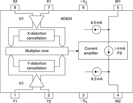
The AD834 is a true linear multiplier with a transfer function of:
Its X and Y offsets are trimmed to 500 μV (3 mV maximum), and it may be used in a wide variety of applications including multipliers (broadband and narrowband), squarers, frequency doublers, and high frequency power measurement circuits. A consideration when using the AD834 is that, because of its very wide bandwidth, its input bias currents, approximately 50 μA/input, must be considered in the design of input circuitry lest, flowing in source resistances, they give rise to unplanned offset voltages.
A basic wideband multiplier using the AD834 is shown in Figure 4-18. The differential output current flows in equal load resistors, R1 and R2, to give a differential voltage output. This is the simplest application circuit for the device. Where only the high frequency outputs are required, transformer coupling may be used, with either simple transformers (see Figure 4-19), or for better wideband performance, transmission line or “Ruthroff” transformers.


Low speed multipliers are also discussed in Chapter 2 (Section 2-11).
SECTION 4-4 Logarithmic Amplifiers
In Chapter 2 (Section 2-8) we discussed low frequency logarithmic (log) amps. In this section we discuss high frequency applications.
The classic diode/op amp (or transistor/op amp) log amp suffers from limited frequency response, especially at low levels. For high frequency applications, detecting and true log architectures are used. Although these differ in detail, the general principle behind their design is common to both: instead of one amplifier having a logarithmic characteristic, these designs use a number of similar cascaded linear stages having well-defined large signal behavior.
Consider N cascaded limiting amplifiers, the output of each driving a summing circuit as well as the next stage (Figure 4-20). If each amplifier has a gain of A dB, the small signal gain of the strip is NA dB.

If the input signal is small enough for the last stage not to limit, the output of the summing amplifier will be dominated by the output of the last stage.
As the input signal increases, the last stage will limit, and so will not add any more gain. Therefore it will now make a fixed contribution to the output of the summing amplifier, but the incremental gain to the summing amplifier will drop to (N −1)A dB. As the input continues to increase, this stage in turn will limit and make a fixed contribution to the output, and the incremental gain will drop to (N −2)AdB, and so forth—until the first stage limits, and the output ceases to change with increasing signal input.
The response curve is thus a set of straight lines as shown in Figure 4-21. The total of these lines, though, is a very good approximation to a logarithmic curve, and in practical cases, is an even better one, because few limiting amplifiers, especially high frequency ones, limit quite as abruptly as this model assumes.
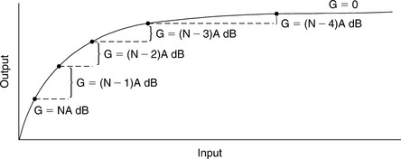
The choice of gain, A, will also affect the log linearity. If the gain is too high, the log approximation will be poor. If it is too low, too many stages will be required to achieve the desired dynamic range. Generally, gains of 10–12 dB (3 times to 4 times) are chosen.
This is, of course, an ideal and very general model—it demonstrates the principle, but its practical implementation at very high frequencies is difficult. Assume that there is a delay in each limiting amplifier of t ns (this delay may also change when the amplifier limits but let’s consider first-order effects!).
The signal which passes through all N stages will undergo delay of Nt ns, while the signal which only passes one stage will be delayed only t ns. This means that a small signal is delayed by Nt ns, while a large one is “smeared,” and arrives spread over Nt ns. A nanosecond equals a foot at the speed of light, so such an effect represents a spread in position of Nt feet in the resolution of a radar system which may be unacceptable in some systems (for most log amp applications this is not a problem).
A solution is to insert delays in the signal paths to the summing amplifier, but this can become complex. Another solution is to alter the architecture slightly so that instead of limiting gain stages, we have stages with small signal gain of A and large signal (incremental) gain of unity (0 dB). We can model such stages as two parallel amplifiers, a limiting one with gain, and a unity gain buffer, which together feed a summing amplifier as shown in Figure 4-22.

Figure 4-22: Structure and performance of “true” log amp element and of a log amp formed by several such elements
The successive detection log amp consists of cascaded limiting stages as described above, but instead of summing their outputs directly, these outputs are applied to detectors, and the detector outputs are summed as shown in Figure 4-23. If the detectors have current outputs, the summing process may involve no more than connecting all the detector outputs together.

Log amps using this architecture have two outputs: the log output and a limiting output. In many applications, the limiting output is not used, but in some (e.g., FM receivers with “S”-meters), both are necessary. The limited output is especially useful in extracting the phase information from the input signal in polar demodulation techniques.
The log output of a successive detection log amplifier generally contains amplitude information, and the phase and frequency information is lost. This is not necessarily the case, however, if a half-wave detector is used, and attention is paid to equalizing the delays from the successive detectors—but the design of such log amps is demanding.
The specifications of log amps will include noise, dynamic range, frequency response (some of the amplifiers used as successive detection log amp stages have low frequency as well as high frequency cutoff), the slope of the transfer characteristic (which is expressed as V/dB or mA/dB depending on whether we are considering a voltage- or current-output device), the intercept point (the input level at which the output voltage or current is zero), and the log linearity (see Figures 4-24).

In the past, it has been necessary to construct high performance, high frequency successive detection log amps (called log strips) using a number of individual monolithic limiting amplifiers such as the Plessey SL-1521-series. Recent advances in IC processes, however, have allowed the complete log strip function to be integrated into a single chip, thereby eliminating the need for costly hybrid log strips.
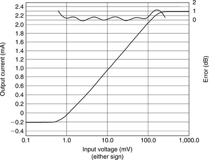
The AD641 log amp contains five limiting stages (10 dB/stage) and five full-wave detectors in a single IC package, and its logarithmic performance extends from DC to 250 MHz. Furthermore, its amplifier and full-wave detector stages are balanced so that, with proper layout, instability from feedback via supply rails is unlikely. A block diagram of the AD641 is shown in Figure 4-25. Unlike many previous IC log amps, the AD641 is laser trimmed to high absolute accuracy of both slope and intercept, and is fully temperature compensated. The transfer function for the AD641 as well as the log linearity is shown in Figure 4-26.

Because of its high accuracy, the actual waveform driving the AD641 must be considered when calculating responses. When a waveform passes through a log function generator, the mean value of the resultant waveform changes. This does not affect the slope of the response, but the apparent intercept is modified.
The AD641 is calibrated and laser trimmed to give its defined response to a DC level or a symmetrical 2 kHz square wave. It is also specified to have an intercept of 2 mV for a sinewave input (that is to say a 2 kHz sinewave of amplitude 2 mV peak (not peak-to-peak) gives the same mean output signal as a DC or square wave signal of 1 mV).
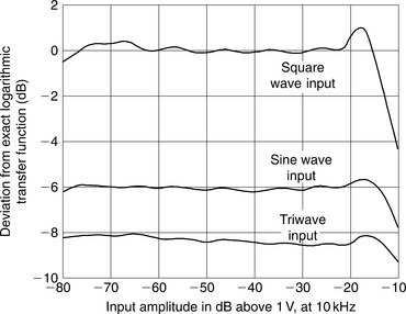
The waveform also affects the ripple or nonlinearity of the log response. This ripple is greatest for DC or square wave inputs because every value of the input voltage maps to a single location on the transfer function, and thus traces out the full nonlinearities of the log response. By contrast, a general time-varying signal has a continuum of values within each cycle of its waveform. The averaged output is thereby “smoothed” because the periodic deviations away from the ideal response, as the waveform “sweeps over” the transfer function, tend to cancel. As is clear in Figure 4-27, this smoothing effect is greatest for a triwave.

Each of the five stages in the AD641 has a gain of 10 dB and a full-wave detected output. The transfer function for the device was shown in Figure 4-26 along with the error curve. Note the excellent log linearity over an input range of 1–100 mV (40 dB)(Figure 4-28). Although well suited to RF applications, the AD641 is DC-coupled throughout. This allows it to be used in low frequency and very low frequency systems, including audio measurements, sonar, and other instrumentation applications requiring operation to low frequencies or even DC.
The limiter output of the AD641 has better than 1.6 dB gain flatness (–44 dBm–0 dBm @ 10.7 MHz) and less than 2° phase variation, allowing it to be used as a polar demodulator.
References: Logarithmic Amplifiers
1 Sheingold D.H., ed. Nonlinear Circuits Handbook. Norwood, MA.: Analog Devices, Inc., 1974.
2 Hughes R.S. Logarithmic Amplifiers. Dedham, MA.: Artech House, Inc., 1986.
3 Barber W.L., Brown E.R. A True Logarithmic Amplifier for Radar IF Applications. IEEE Journal of Solid State Circuits. 1980;Vol. SC-15(3):291–295. June
4 Broadband Amplifier Applications. MA.: Plessey Co. Publication P.S. Norwood; 1984. 1938 September.
5 Gay M.S. SL521 Application Note. Plessey Co., 1966.
6 Amplifier Applications Guide. Norwood, MA.: Analog Devices, Inc.; 1992. Section 9.
7 Ask the Applications Engineer −28 Logarithmic Amplifiers-Explained. Analog Dialogue. Vol. 33(3), 1999. March.
8 Detecting Fast RF Bursts Using Log Amps. Analog Dialogue. Vol. 36(5), 2002. September-October.
9 R. Moghimi, “Log-Ratio Amplifier has Six-decade Dynamic Range,” EDN, November, 2003.
SECTION 4-5 Tru-Power Detectors
In many systems, cellular phones as an example, monitoring of the transmit signal amplitude is required. The AD8362 is a true root mean square (RMS)-responding power detector that has a 60 dB measurement range (Figures 4-29 and 4-30). It is intended for use in a variety of high frequency communication systems and in instrumentation requiring an accurate response to signal power. It can operate from arbitrarily low frequencies to over 2.7 GHz and can accept inputs that have RMS values from 1 mV to at least 1 VRMS, with peak crest factors of up to 6, exceeding the requirements for accurate measurement of CDMA signals. Unlike earlier RMS-to-DC converters, the response bandwidth is completely independent of the signal magnitude. The −3 dB point occurs at about 3.5 GHz.


The input signal is applied to a resistive ladder attenuator that comprises the input stage of a variable gain amplifier (VGA). The 12-tap points are smoothly interpolated using a proprietary technique to provide a continuously variable attenuator, which is controlled by a voltage applied to the VSET pin. The resulting signal is applied to a high performance broadband amplifier. Its output is measured by an accurate square-law detector cell. The fluctuating output is then filtered and compared with the output of an identical squarer, whose input is a fixed DC voltage applied to the VTGT pin, usually the accurate reference of 1.25 V provided at the VREF pin.
The difference in the outputs of these squaring cells is integrated in a high gain error amplifier, generating a voltage at the VOUT pin with rail-to-rail capabilities. In a controller mode, this low noise output can be used to vary the gain of a host system’s RF amplifier, thus balancing the setpoint against the input power.
Optionally, the voltage at VSET may be a replica of the RF signal’s AM, in which case the overall effect is to remove the modulation component prior to detection and lowpass filtering. The corner frequency of the averaging filter may be lowered without limit by adding an external capacitor at the CLPF pin.
The AD8362 can be used to determine the true power of a high frequency signal having a complex low FM envelope (or simply as a low frequency RMS voltmeter). The high pass corner generated by its offset-nulling loop can be lowered by a capacitor added on the CHPF pin (Figure 4-31).

Used as a power measurement device, VOUT is strapped to VSET, and the output is then proportional to the logarithm of the RMS value of the input; that is, the reading is presented directly in decibels, and is conveniently scaled 1 V/decade, that is, 50 mV/dB; other slopes are easily arranged. In controller modes, the voltage applied to VSET determines the power level required at the input to null the deviation from the setpoint. The output buffer can provide high load currents.
The AD8362 can be powered down by a logic high applied to the PWDN pin (i.e., the consumption is reduced to about 1.3 mW). It powers up within about 20 μs to its nominal operating current of 20 mA at 25°C.
SECTION 4-6 VGAs
Voltage Controlled Amplifiers
Many monolithic VGAs use techniques that share common principles that are broadly classified as translinear, a term referring to circuit cells whose functions depend directly on the very predictable properties of BJTs, notably the linear dependence of their transconductance on collector current. Since the discovery of these cells in 1967, and their commercial exploitation in products developed during the early 1970s, accurate wide bandwidth analog multipliers, dividers, and VGAs have invariably employed translinear principles.
While these techniques are well understood, the realization of a high performance VGA requires special technologies and attention to many subtle details in its design. As an example, the AD8330 is fabricated on a proprietary silicon-on-insulator, complementary bipolar IC process and draws on decades of experience in developing many leading-edge products using translinear principles to provide an unprecedented level of versatility. Figure 4-32 shows a basic representative cell comprising just four transistors. This, or a very closely related form, is at the heart of most translinear multipliers, dividers, and VGAs. The key concepts are as follows: First, the ratio of the currents in the left-hand and right-hand pairs of transistors are identical; this is represented by the modulation factor, x, which may have values between −1 and +1. Second, the input signal is arranged to modulate the fixed tail current ID to cause the variable value of x introduced in the left-hand pair to be replicated in the right-hand pair, and thus generate the output by modulating its nominally fixed tail current IN. Third, the current gain of this cell is very exactly G = IN/ID over many decades of variable bias current.

In practice, the realization of the full potential of this circuit involves many other factors, but these three elementary ideas remain essential. By varying IN, the overall function is that of a two-quadrant analog multiplier, exhibiting a linear relationship to both the signal modulation factor x and this numerator current. On the other hand, by varying ID, a two-quadrant analog divider is realized, having a hyperbolic gain function with respect to the input factor x, controlled by this denominator current. The AD8330 exploits both modes of operation. However, since a hyperbolic gain function is generally of less value than one in which the decibel gain is a linear function of a control input, a special interface is included to provide either increasing or decreasing exponential control of ID.
The VGA core of the AD8330 (Figure 4-33) contains a much elaborated version of the cell shown in Figure 4-32. The current called ID is controlled exponentially (linear in decibels) through the decibel gain interface at the pin VDBS and its local common CMGN. The gain span (i.e., the decibel difference between maximum and minimum values) provided by this control function is slightly more than 50 dB. The absolute gain from input to output is a function of source and load impedance and also depends on the voltage on a second gain—control pin, VMAG.

X-AMP®
Most voltage controlled amplifiers (VCAs) made with analog multipliers have gain which is linear in volts with respect to the control voltage; moreover they tend to be noisy. There is a demand, however, for a VCA which combines a wide gain range with constant bandwidth and phase, low noise with large signal-handling capabilities, and low distortion with low power consumption, while providing accurate, stable, linear-in-dB gain. The X-AMP® family achieves these demanding and conflicting objectives with a unique and elegant solution (for exponential amplifier). The concept is simple: a fixed-gain amplifier follows a passive, broadband attenuator equipped with special means to alter its attenuation under the control of a voltage (see Figure 4-34). The amplifier is optimized for low input noise, and negative feedback is used to accurately define its moderately high gain (about 30–40 dB) and minimize distortion. Because this amplifier’s gain is fixed, so also are its AC and transient response characteristics, including distortion and group delay; Because its gain is high, its input is never driven beyond a few millivolts. Therefore, it is always operating within its small signal response range.

The attenuator is a 7-section (8-tap) R–2R ladder network. The voltage ratio between all adjacent taps is exactly 2, or 6.02 dB. This provides the basis for the precise linear-in-dB behavior. The overall attenuation is 42.1 4 dB. As will be shown, the amplifier’s input can be connected to any one of these taps, or even interpolated between them, with only a small deviation error of about ±0.2 dB. The overall gain can be varied all the way from the fixed (maximum) gain to a value 42.14 dB less. For example, in the AD600, the fixed gain is 41.07 dB (a voltage gain of 113); using this choice, the full gain range is −1.07 dB to +41.07 dB. The gain is related to the control voltage by the relationship GdB = 32 VG + 20 where VG is in volts.
The gain at VG = 0 is laser trimmed to an absolute accuracy of ±0.2 dB. The gain scaling is determined by an on-chip bandgap reference (shared by both channels), laser trimmed for high accuracy and low temperature coefficient. Figure 4-35 shows the gain versus the differential control voltage for both the AD600 and the AD602.

In order to understand the operation of the X-AMP® family, consider the simplified diagram shown in Figure 4-36. Notice that each of the eight taps is connected to an input of one of eight bipolar differential pairs, used as current controlled transconductance (gm) stages; the other input of all these gm stages is connected to the amplifier’s gain-determining feedback network, RF1/RF2. When the emitter bias current, IE, is directed to one of the eight transistor pairs (by means not shown here), it becomes the input stage for the complete amplifier.

When IE is connected to the pair on the left-hand side, the signal input is connected directly to the amplifier, giving the maximum gain. The distortion is very low, even at high frequencies, due to the careful open-loop design, aided by the negative feedback. If IE were now to be abruptly switched to the second pair, the overall gain would drop by exactly 6.02 dB, and the distortion would remain low, because only one gm stage remains active.
In reality, the bias current is gradually transferred from the first pair to the second. When IE is equally divided between two gm stages, both are active, and the situation arises where we have an op amp with two input stages fighting for control of the loop, one getting the full signal and the other getting a signal exactly half as large.
Analysis shows that the effective gain is reduced, not by 3 dB, as one might first expect, but rather by 20 log 1.5, or 3.52 dB. This error, when divided equally over the whole range, would amount to a gain ripple of ±0.25 dB; however, the interpolation circuit actually generates a Gaussian distribution of bias currents, and a significant fraction of IE always flows in adjacent stages. This smoothes the gain function and actually lowers the ripple. As IE moves further to the right, the overall gain progressively drops.
The total input-referred noise of the X-AMP® is 1.4 nV/![]() ; only slightly more than the thermal noise of a 100 Ω resistor, which is 1.29 nV/
; only slightly more than the thermal noise of a 100 Ω resistor, which is 1.29 nV/![]() at 25°C. The input-referred noise is constant regardless of the attenuator setting; therefore, the output noise is always constant and independent of gain.
at 25°C. The input-referred noise is constant regardless of the attenuator setting; therefore, the output noise is always constant and independent of gain.
The AD8367 is a high performance 45 dB VGA with linear-in-dB gain control for use from low frequencies up to several hundred megahertz (Figure 4-37). It includes an onboard detector which is used to build an automatic gain-controlled amplifier. The range, flatness, and accuracy of the gain response are achieved using Analog Devices’ X-AMP® architecture, the most recent in a series of powerful proprietary concepts for variable gain applications, which far surpasses what can be achieved using competing techniques.

The input is applied to a 200 Ω resistive ladder network, having nine sections each of 5 dB loss, for a total attenuation of 45 dB. At maximum gain, the first tap is selected; at progressively lower gains, the tap moves smoothly and continuously toward higher attenuation values. The attenuator is followed by a 42.5 dB fixed-gain feedback amplifier—essentially an operational amplifier with a gain bandwidth product of 100 GHz—and is very linear, even at high frequencies. The output third-order intercept is +20 dBV at 100 MHz (+27 dBm re200 Ω), measured at an output level of 1 Vp–p with VS = 5 V. The analog gain-control interface is very simple to use. It is scaled at 20 mV/dB, and the control voltage, VGAIN, runs from 50 mV at −2.5 dB to 950 mV at +42.5 dB. In the inverse-gain mode of operation, selected by a simple pin-strap, the gain decreases from +42.5 dB at VGAIN = 50 mV to −2.5 dB at VGAIN = 950 mV. This inverse mode is needed in AGC applications, which are supported by the integrated square-law detector, whose setpoint is chosen to level the output to 354 mVRMS, regardless of the waveshape. A single external capacitor sets up the loop averaging time.
Digitally Controlled VGAs
In some cases it may be advantageous to have the control of the signal level under digital control. The AD8370 is a low cost, digitally controlled VGA that provides precision gain control, high IP3, and low noise figure (Figure 4-38). The AD8370 has excellent distortion performance and wide bandwidth. For wide input, dynamic range applications, the AD8370 provides two input ranges: high gain mode and low gain mode. A Vernier 7-bit transconductance (Gm) stage provides 28 dB of gain range at better than 2 dB resolution, and 22 dB of gain range at better than 1 dB resolution. A second gain range, 17 dB higher than the first, can be selected to provide improved noise performance. The AD8370 is powered on by applying the appropriate logic level to the PWUP pin. When powered down, the AD8370 consumes less than 4 mA and offers excellent input to output isolation. The gain setting is preserved when operating in a power-down mode.

Gain control of the AD8370 is through a serial 8-bit gain-control word. The most significant bit (MSB) selects between the two gain ranges, and the remaining 7 bits adjust the overall gain in precise linear gain steps.
VGAs are also discussed in Chapter 2 (Sections 2-3 and 2-14).
1 B. Gilbert, “A Low Noise Wideband Variable-Gain Amplifier Using an Interpolated Ladder Attenuator,” IEEE ISSCC Technical Digest, 1991, pp. 280, 281, 330.
2 Gilbert B. “A Monolithic Microsystem for Analog Synthesis of Trigonometric Functions and Their Inverses”. IEEE Journal of Solid State Circuits. 1982;Vol. SC-17(6):1179–1191. December
3 Linear Design Seminar, Analog Devices, 1995, Section 3.
4 Newman E. X-amp, A New 45-dB, 500-MHz Variable-Gain Amplifier (VGA) Simplifies Adaptive Receiver Designs. Analog Dialogue. Vol. 36(1), 2002. January–February.
5 B. Gilbert and E. Nash, A 10.7 MHz, 120 dB Logarithmic Amp … An extract from “Demodulating Logamps Bolster Wide-Dynamic-Range Measurements” Microwaves and RF, March, 1998.
6 S. Bonadio and E. Newman, “Variable Gain Amplifiers Enable Cost Effective IF Sampling Receiver Designs,” Microwave Product Digest, October, 2003.
7 E. Newman and S. Lee, “Linear-in-dB Variable Gain Amplifier Provides True RMS Power nts,” Wireless Design 2004.
8 P. Halford and E. Nash, “Integrated VGA Aids Precise Gain Control,” Microwaves & RF, March, 2002.
SECTION 4-7 Direct Digital Synthesis
A frequency synthesizer generates multiple frequencies from one or more frequency references. These devices have been used for decades, especially in communications systems. Many are based on switching and mixing frequency outputs from a bank of crystal oscillators. Others have been based on well understood techniques utilizing phase-locked loops (PLLs). These will be discussed in the following section.
DDS (Direct Digital Synthesis)
With the widespread use of digital techniques in instrumentation and communications systems, a digitally controlled method of generating multiple frequencies from a reference frequency source has evolved called direct digital synthesis (DDS). The basic architecture is shown in Figure 4-39. In this simplified model, a stable clock drives a programmable-read-only memory (PROM) which stores one or more integral number of cycles of a sinewave (or other arbitrary waveform, for that matter). As the address counter steps through each memory location, the corresponding digital amplitude of the signal at each location drives a digital-to-analog converter (DAC) which in turn generates the analog output signal. The spectral purity of the final analog output signal is determined primarily by the DAC. The phase noise is basically that of the reference clock.

Because a DDS system is a sampled data system, all the issues involved in sampling must be considered: quantization noise, aliasing, filtering, etc. For instance, the higher order harmonics of the DAC output frequencies fold back into the Nyquist bandwidth, making them unfilterable; whereas, the higher order harmonics of the output of PLL-based synthesizers can be filtered. There are other considerations which will be discussed shortly.
A fundamental problem with this simple DDS system is that the final output frequency can be changed only by changing the reference clock frequency or by reprogramming the PROM, making it rather inflexible. A practical DDS system implements this basic function in a much more flexible and efficient manner using digital hardware called a numerically controlled oscillator (NCO). A block diagram of such a system is shown in Figure 4-40.

The heart of the system is the phase accumulator whose content is updated once each clock cycle (Figure 4-41). Each time the phase accumulator is updated, the digital number, M, stored in the delta phase register is added to the number in the phase accumulator register. Assume that the number in the delta phase register is 00 … 01 and that the initial content of the phase accumulator is 00 … 00. The phase accumulator is updated by 00 … 01 on each clock cycle. If the accumulator is 32-bits wide, 232 clock cycles (over 4 billion) are required before the phase accumulator returns to 00 … 00, and the cycle repeats.

The truncated output of the phase accumulator serves as the address to a sine (or cosine) lookup table. Each address in the lookup table corresponds to a phase point on the sinewave from 0° to 360°. The lookup table contains the corresponding digital amplitude information for one complete cycle of a sinewave. (Actually, only data for 90° is required because the quadrature data are contained in the two MSBs.) The lookup table therefore maps the phase information from the phase accumulator into a digital amplitude word, which in turn drives the DAC.
Consider the case for n = 32, and M = 1. The phase accumulator steps through each of 232 possible outputs before it overflows and restarts. The corresponding output sinewave frequency is equal to the input clock frequency divided by 232. If M = 2, then the phase accumulator register “rolls over” twice as fast, and the output frequency is doubled. This can be generalized as follows.
For an n-bit phase accumulator (n generally ranges from 24 to 32 in most DDS systems), there are 2n possible phase points. The digital word in the delta phase register, M, represents the amount the phase accumulator is incremented each clock cycle. If fc is the clock frequency, then the frequency of the output sinewave is equal to:
This equation is known as the DDS “tuning equation.” Note that the frequency resolution of the system is equal to fc/2n. For n = 32, the resolution is greater than one part in four billion! In a practical DDS system, all the bits out of the phase accumulator are not passed on to the lookup table but are truncated, leaving only the first 13–15 MSBs. This reduces the size of the lookup table and does not affect the frequency resolution. The phase truncation only adds a small but acceptable amount of phase noise to the final output. The resolution of the DAC is typically 2–4 bits less than the width of the lookup table. Even a perfect N-bit DAC will add quantization noise to the output. Figure 4-42 shows the calculated output spectrum for a 32-bit phase accumulator, 15-bit phase truncation, and an ideal 12-bit DAC. The value of M was chosen so that the output frequency was slightly offset from 0.25 times the clock frequency. Note that the spurs caused by the phase truncation and the finite DAC resolution are all at least 90 dB below the full-scale output. This performance far exceeds that of any commercially available 12-bit DAC and is adequate for most applications.

Figure 4-42: Calculated output spectrum shows 90 dB SFDR for a 15-bit phase truncation and an ideal 12-bit DAC
The basic DDS system described above is extremely flexible and has high resolution. The frequency can be changed instantaneously with no phase discontinuity by simply changing the contents of the M-register. However, practical DDS systems first require the execution of a serial, or byte-loading sequence to get the new frequency word into an internal buffer register which precedes the parallel-output M-register. This is done to minimize package pin count. After the new word is loaded into the buffer register, the parallel-output delta phase register is clocked, thereby changing all the bits simultaneously. The number of clock cycles required to load the delta phase buffer register determines the maximum rate at which the output frequency can be changed.
Aliasing in DDS Systems
There is one important limitation to the range of output frequencies that can be generated from the simple DDS system. The Nyquist criteria state that the clock frequency (sample rate) must be at least twice the output frequency. Practical limitations restrict the actual highest output frequency to about 1/3 the clock frequency. Figure 4-43 shows the output of a DAC in a DDS system where the output frequency is 30 MHz and the clock frequency is 100 MHz. An antialiasing filter must follow the reconstruction DAC to remove the lower image frequency (100–30 = 70 MHz) as shown in Figure 4-43.

Note that the amplitude response of the DAC output (before filtering) follows a sin(x)/x response with zeros at the clock frequency and multiples thereof. The exact equation for the normalized output amplitude, A(fo), is given by:
 (4-9)
(4-9)where fo is the output frequency and fc is the clock frequency.
This rolloff is because the DAC output is not a series of zero-width impulses (as in a perfect re-sampler), but a series of rectangular pulses whose width is equal to the reciprocal of the update rate. The amplitude of the sin(x)/x response is down 3.92 dB at the Nyquist frequency (1/2 the DAC update rate). In practice, the transfer function of the reconstruction (antialiasing) filter can be designed to compensate for the sin(x)/x rolloff so that the overall frequency response is relatively flat up to the maximum output DAC frequency (generally 1/3 the update rate).
Another important consideration is that, unlike a PLL-based system, the higher order harmonics of the fundamental output frequency in a DDS system will fold back into the baseband because of aliasing. These harmonics cannot be removed by the antialiasing filter. For instance, if the clock frequency is 100 MHz, and the output frequency is 30 MHz, the second harmonic of the 30 MHz output signal appears at 60 MHz (out of band), but also at 100–60 = 40 MHz (the aliased component). Similarly, the third harmonic (which would occur at 90 MHz) appears in band at 100–90 = 10 MHz, and the fourth harmonic at 120–100 MHz = 20 MHz. Higher order harmonics also fall within the Nyquist bandwidth (DC to fc/2). The location of the first four harmonics is shown in Figure 4-43.
DDS Systems as ADC Clock Drivers
DDS systems such as the AD9850 provide an excellent method of generating the sampling clock to the ADC, especially when the ADC sampling frequency must be under software control and locked to the system clock (see Figure 4-44). The true DAC output current Iout, drives a 200 Ω, 42 MHz lowpass filter which is source and load terminated, thereby making the equivalent load 100 Ω. The filter removes spurious frequency components above 42 MHz. The filtered output drives one input of the AD9850 internal comparator. The complementary DAC output current drives a 100 Ω load. The output of the 100 kΩ resistor divider placed between the two outputs is decoupled and generates the reference voltage for the internal comparator.

The comparator output has a 2 ns rise and fall time and generates a TTL/CMOS-compatible square wave. The jitter of the comparator output edges is less than 20 ps RMS. True and complementary outputs are available if required.
In the circuit shown (Figure 4-44), the total output RMS jitter for a 40 MSPS ADC clock is 50 ps RMS, and the resulting degradation in SNR must be considered in wide dynamic range applications
AM in a DDS System
AM in a DDS system can be accomplished by placing a digital multiplier between the lookup table and the DAC input as shown in Figure 4-45. Another method to modulate the DAC output amplitude is to vary the reference voltage to the DAC. In the case of the AD9850, the bandwidth of the internal reference control amplifier is approximately 1 MHz. This method is useful for relatively small output amplitude changes as long as the output signal does not exceed the +1 V compliance specification.

Spurious Free Dynamic Range Considerations in DDS Systems
In many DDS applications, the spectral purity of the DAC output is of primary concern. Unfortunately, the measurement, prediction, and analysis of this performance is complicated by a number of interacting factors.
Even an ideal N-bit DAC will produce harmonics in a DDS system. The amplitude of these harmonics is highly dependent on the ratio of the output frequency to the clock frequency. This is because the spectral content of the DAC quantization noise varies as this ratio varies, even though its theoretical RMS value remains equal to q/12 (where q is the weight of the least significant bit (LSB)). The assumption that the quantization noise appears as white noise and is spread uniformly over the Nyquist bandwidth is simply not true in a DDS system (it is more apt to be a true assumption in an ADC-based system, because the ADC adds a certain amount of noise to the signal which tends to “dither” or randomize the quantization error. However, a certain amount of correlation still exists). For instance, if the DAC output frequency is set to an exact submultiple of the clock frequency, then the quantization noise will be concentrated at multiples of the output frequency (i.e., it is highly signal dependent). If the output frequency is slightly offset, however, the quantization noise will become more random, thereby giving an improvement in the effective spurious free dynamic range (SFDR).
This is illustrated in Figure 4-46, where a 4096 (4 k) point Fourier transform (FFT) is calculated based on digitally generated data from an ideal 12-bit DAC. In the left-hand diagram, the ratio between the clock frequency and the output frequency was chosen to be exactly 32 (128 cycles of the sinewave in the FFT record length), yielding an SFDR of about 78 dBc. In the right-hand diagram, the ratio was changed to 32.25196850394 (127 cycles of the sinewave within the FFT record length), and the effective SFDR is now increased to 92 dBc. In this ideal case, we observed a change in SFDR of 14 dB just by slightly changing the frequency ratio.

Figure 4-46: Effect of ratio of clock to output frequency on theoretical 12-bit DAC SFDR using 4096-point FFT
Best SFDR can therefore be obtained by the careful selection of the clock and output frequencies. However, in some applications, this may not be possible. In ADC-based systems, adding a small amount of random noise to the input tends to randomize the quantization errors and reduce this effect. The same thing can be done in a DDS system as shown in Figure 4-47 (Reference 5). The pseudo-random digital noise generator output is added to the DDS sine amplitude word before being loaded into the DAC. The amplitude of the digital noise is set to about 1/2 LSB. This accomplishes the randomization process at the expense of a slight increase in the overall output noise floor. In most DDS applications, however, there is enough flexibility in selecting the various frequency ratios so that dithering is not required.

References: Direct Digital Synthesis
1 Ask the Application Engineer—33: All About Direct Digital Synthesis. Analog Dialogue. Vol. 38, 2004. August.
2 Innovative Mixed-Signal Chipset Targets Hybrid-Fiber Coaxial Cable Modems. Analog Dialogue. Vol. 31(3), 1997.
3 Single-Chip Direct Digital Synthesis vs. the Analog PLL. Analog Dialogue. Vol. 30(3), 1996.
4 Kroupa V., ed. Direct Digital Frequency Synthesizers. Wiley-IEEE Press, 1998.
5 D. Brandon, DDS Design, Analog Devices, Inc.
6 Jitter Reduction in DDS Clock Generator Systems Copyright ©. Analog Devices, Inc.
7 A Technical Tutorial on Digital Signal Synthesis Copyright © 1999 Analog Devices, Inc.
SECTION 4-8 PLLs
A PLL is a feedback system combining a voltage-controlled oscillator (VCO) and a phase comparator so connected that the oscillator maintains a constant phase angle relative to a reference signal. PLLs can be used, for example, to generate stable output frequency signals from a fixed low frequency signal. The PLL can be analyzed in general as a negative feedback system with a forward gain term and a feedback term. A simple block diagram of a voltage-based negative feedback system is shown in Figure 4-48.

In a PLL, the error signal from the phase comparator is proportional to the relative phase of the input and feedback signals. The average output of the phase detector will be constant when the input and feedback signals are the same frequency. The usual equations for a negative feedback system apply.
Because of the integration in the loop, at low frequencies the steady state gain, G(s), is high and,
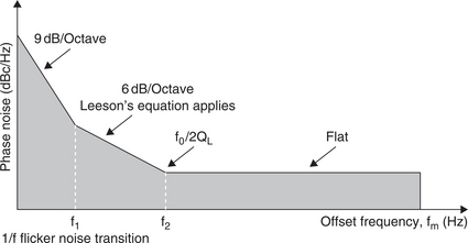
The components of a PLL that contribute to the loop gain include (Figure 4-49):
1. The phase detector (PD) and charge pump (CP).
2. The loop filter, with a transfer function of Z(s).

If a linear element like a four-quadrant multiplier is used as the phase detector, and the loop filter and VCO are also analog elements, this is called an analog, or linear PLL (LPLL). If a digital phase detector (Exclusive-or (EXOR) gate or J–K flip-flop) is used, and everything else stays the same, the system is called a digital PLL (DPLL). If the PLL is built exclusively from digital blocks, without any passive components or linear elements, it becomes an all-digital PLL (ADPLL).
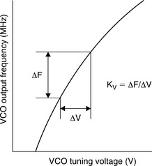
In commercial PLLs, the phase detector and CP together form the error detector block. When Fo × N FREF, the error detector will output source/sink current pulses to the lowpass loop filter. This smoothes the current pulses into a voltage which in turn drives the VCO. The VCO frequency will then increase or decrease as necessary, by Kv × ΔV, where Kv is the VCO sensitivity in MHz/V and ΔV is the change in VCO input voltage. This will continue until e(s) is zero and the loop is locked. The CP and VCO thus serves as an integrator, seeking to increase or decrease its output frequency to the value required so as to restore its input (from the phase detector) to zero.
The overall transfer function (CLG or closed-loop gain) of the PLL can be expressed simply by using the CLG expression for a negative feedback system as given above.
When GH is much greater than 1, we can say that the closed-loop transfer function for the PLL system is N and so:
The loop filter is a lowpass type, typically with one pole and one zero. The transient response of the loop depends on:
All of the above must be taken into account when designing the loop filter. In addition, the filter must be designed to be stable (usually a phase margin of 90° is recommended). The 3-dB cutoff frequency of the response is usually called the loop bandwidth, BW. Large loop bandwidths result in very fast transient response. However, this is not always advantageous, since there is a tradeoff between fast transient response and reference spur attenuation.
PLL Synthesizer Basic Building Blocks
A PLL synthesizer can be considered in terms of several basic building blocks. Already touched on, they will now be dealt with in greater detail:
The heart of a synthesizer is the phase detector—or PFD. This is where the reference frequency signal is compared with the signal fed back from the VCO output, and the resulting error signal is used to drive the loop filter and VCO. In a DPLL the phase detector or PFD is a logical element.
The three most common implementations are:
Here we will consider only the PFD, the element used in the ADF411X and ADF421X synthesizer families, because—unlike the EXOR gate and the J–K flip-flop—its output is a function of both the frequency difference and the phase difference between the two inputs when it is in the unlocked state. One implementation of a PFD, basically consisting of two D-type flip-flops is shown in Figure 4-51. One Q output enables a positive current source, and the other Q output enables a negative current source. Assuming that, in this design, the D-type flip-flop is positive-edge triggered, the states are these (Q1, Q2):
11—both outputs high, is disabled by the AND gate (U3) back to the CLR pins on the flip-flops.
00—both P1 and N1 are turned off and the output, OUT, is essentially in a high impedance state.
10—P1 is turned on, N1 is turned off, and the output is at V +.
01—P1 is turned off, N1 is turned on, and the output is at V−.

Consider now how the circuit behaves if the system is out of lock and the frequency at + IN is much higher than the frequency at –IN, as exemplified in Figure 4-52.
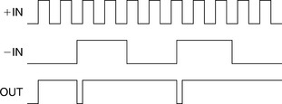
Since the frequency at +IN is much higher than that at –IN, the output spends most of its time in the high state. The first rising edge on +IN forces the output high and this state is maintained until the first rising edge occurs on −IN. In a practical system this means that the output, and thus the input to the VCO, is driven higher, resulting in an increase in frequency at −IN. This is exactly what is desired. If the frequency on + IN were much lower than on −IN, the opposite effect would occur. The output at OUT would spend most of its time in the low condition. This would have the effect of driving the VCO in the negative direction and again bring the frequency at −IN much closer to that at + IN, to approach the locked condition. Figure 4-53 shows the waveforms when the inputs are frequency-locked and close to phase lock.
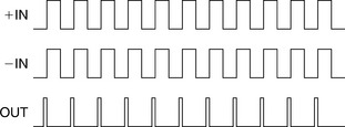
Since +IN is leading –IN, the output is a series of positive current pulses. These pulses will tend to drive the VCO so that the –IN signal become phase-aligned with that on + IN.
When this occurs, if there were no delay element between U3 and the CLR inputs of U1 and U2, it would be possible for the output to be in high impedance state, producing neither positive nor negative current pulses. This would not be a good situation. The VCO would drift until a significant phase error developed and started producing either positive or negative current pulses once again. Over a relatively long period of time, the effect of this cycling would be for the output of the CP to be modulated by a signal that is a subharmonic of the PFD input reference frequency. Since this could be a low frequency signal, it would not be attenuated by the loop filter and would result in very significant spurs in the VCO output spectrum, a phenomenon known as the backlash effect. The delay element between the output of U3 and the CLR inputs of U1 and U2 ensures that it does not happen. With the delay element, even when the + IN and −IN are perfectly phase-aligned, there will still be a current pulse generated at the CP output. The duration of this delay is equal to the delay inserted at the output of U3 and is known as the antibacklash pulse width.
The Reference Counter
In the classical integer-N synthesizer, the resolution of the output frequency is determined by the reference frequency applied to the phase detector. So, for example, if 200 kHz spacing is required (as in GSM phones), then the reference frequency must be 200 kHz. However, getting a stable 200 kHz frequency source is not easy. A sensible approach is to take a good crystal-based high frequency source and divide it down. For example, the desired frequency spacing could be achieved by starting with a 10 MHz frequency reference and dividing it down by 50. This approach is shown in the diagram in Figure 4-54.

The Feedback Counter, N
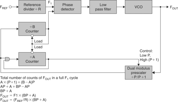
The N counter, also known as the N divider, is the programmable element that sets the relationship between the input and output frequencies in the PLL. The complexity of the N counter has grown over the years. In addition to a straightforward N counter, it has evolved to include a prescaler, which can have a dual modulus.
This structure has emerged as a solution to the problems inherent in using the basic divide-by-N structure to feed back to the phase detector when very high frequency outputs are required. For example, let’s assume that a 900 MHz output is required with 10 kHz spacing. A 10 MHz reference frequency might be used, with the R divider set at 1,000. Then, the N-value in the feedback would need to be of the order of 90,000. This would mean at least a 17-bit counter capable of operating at an input frequency of 900 MHz.
To handle this range, it makes sense to precede the programmable counter with a fixed counter element to bring the very high input frequency down to a range at which standard CMOS counters will operate. This counter, called a prescaler, is shown in Figure 4-55.

However, using a standard prescaler introduces other complications. The system resolution is now degraded (F1 × P). This issue can be addressed by using a dual-modulus prescaler (Figure 4-56). It has the advantages of the standard prescaler but without any loss in system resolution. A dual-modulus prescaler is a counter whose division ratio can be switched from one value to another by an external control signal. By using the dual-modulus prescaler with an A and B counter, one can still maintain output resolution of F1.
However, the following conditions must be met:
1. The output signals of both counters are high if the counters have not timed out.
2. When the B counter times out, its output goes low, and it immediately loads both counters to their preset values.
3. The value loaded to the B counter must always be greater than that loaded to the A counter.
Assume that the B counter has just timed out and both counters have been reloaded with the values A and B. Let’s find the number of VCO cycles necessary to get to the same state again.
As long as the A counter has not timed out, the prescaler is dividing down by P + 1. So, both the A and B counters will count down by 1 every time the prescaler counts (P+ 1) VCO cycles. This means the A counter will time out after ((P + 1) × A) VCO cycles.
At this point the prescaler is switched to divide-by-P. It is also possible to say that at this time the B counter still has (B – A) cycles to go before it times out. How long will it take to do this: ((B – A) × P). The system is now back to the initial condition where we started.
The total number of VCO cycles needed for this to happen is:
When using a dual-modulus prescaler, it is important to consider the lowest and highest values of N. What we really want here is the range over which it is possible to change N in discrete integer steps. Consider the expression N = A + BP. To ensure a continuous integer spacing for N, A must be in the range 0 to (P −1). Then, every time B is incremented there is enough resolution to fill in all the integer values between BP and (B + 1)P. As was already noted for the dual-modulus prescaler, B must be greater than or equal to A for the dual-modulus prescaler to work. From these we can say that the smallest division ratio possible while being able to increment in discrete integer steps is:
The highest value of N is given by:
In this case AMAX and BMAX are simply determined by the size of the A and B counters.
Now for a practical example with the ADF4111, let’s assume that the prescaler is programmed to 32/33. The A counter is 6-bits wide, which means A can be 26 −1 = 63. The B counter is 13-bits wide, which means B can be 213 −1 = 8191.
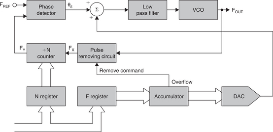
Fractional-N Synthesizers
Many of the emerging wireless communication systems have a need for faster switching and lower phase noise in the LO. Integer-N synthesizers require a reference frequency that is equal to the channel spacing. This can be quite low and thus necessitates a high N. This high N produces a phase noise that is proportionally high. The low reference frequency limits the PLL lock time. Fractional-N synthesis is a means of achieving both low phase noise and fast lock time in PLLs. The technique was originally developed in the early 1970s. This early work was done mainly by Hewlett Packard and Racal. The technique originally went by the name of “digiphase,” but it later became popularly named fractional-N. In the standard synthesizer, it is possible to divide the RF signal by an integer only. This necessitates the use of a relatively low reference frequency (determined by the system channel spacing) and results in a high value of N in the feedback. Both of these facts have a major influence on the system settling time and the system phase noise. The low reference frequency means a long settling time, and the high value of N means larger phase noise.
If division by a fraction could occur in the feedback, it would be possible to use a higher reference frequency and still achieve the desired channel spacing. This lower fractional number would also mean lower phase noise.
In fact it is possible to implement division by a fraction over a long period of time by alternately dividing by two integers (divide by 2.5 can be achieved by dividing successively by 2 and 3). So, how does one divide by X or (X + 1) (assuming that the fractional number is between these two values)?
Well, the fractional part of the number can be allowed to accumulate at the reference frequency rate. Then every time the accumulator overflows, this signal can be used to change the N divide ratio. This is done in Figure 4-57 by removing one pulse being fed to the N counter. This effectively increases the divide ratio by one every time the accumulator overflows. Also, the bigger the number in the F-register, the more often the accumulator overflows and the more often division by the larger number occurs. This is exactly what is desired from the circuit. There are some added complications, however. The signal being fed to the phase detector from the divide-by-N circuit is not a uniform stream of regularly spaced pulses. Instead the pulses are being modulated at a rate determined by the reference frequency and the programmed fraction. This in turn modulates the phase detector output and drives the VCO input. The end result is a high spurious content at the output of the VCO. Major efforts are currently under way to minimize these spurs. Up to now, monolithic fractional-N synthesizers have failed to live up to expectations but the eventual benefits that may be realized mean that development is continuing at a rapid pace.
Noise in Oscillator Systems
In any oscillator design, frequency stability is of critical importance. We are interested in both long-term and short-term stability. Long-term frequency stability is concerned with how the output signal varies over a long period of time (hours, days, or months). It is usually specified as the ratio, Δf/f for a given period of time, expressed as a percentage or in dB. Short-term stability, on the other hand, is concerned with variations that occur over a period of seconds or less. These variations can be random or periodic. A spectrum analyzer can be used to examine the short-term stability of a signal. Figure 4-58 shows a typical spectrum, with random and discrete frequency components causing both a broad skirt and spurious peaks.
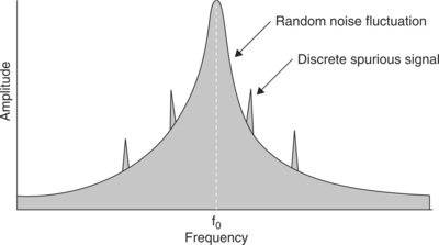
The discrete spurious components could be caused by known clock frequencies in the signal source, power line interference, and mixer products. The broadening caused by random noise fluctuation is due to phase noise. It can be the result of thermal noise, shot noise, and/or flicker noise in active and passive devices.
Phase Noise in VCOs
Before we look at phase noise in a PLL system, it is worth considering the phase noise in a VCO. An ideal VCO would have no phase noise. Its output as seen on a spectrum analyzer would be a single spectral line. In practice, of course, this is not the case. There will be jitter on the output, and a spectrum analyzer would show phase noise. To help understand phase noise, consider a phasor representation, such as that shown in Figure 4-59.

A signal of angular velocity ωO and peak amplitude VSPK is shown. Superimposed on this is an error signal of angular velocity ωm. ΔθRMS represents the RMS value of the phase fluctuations and is expressed in RMS degrees.
In many radio systems, an overall integrated phase error specification must be met. This overall phase error is made up of the PLL phase error, the modulator phase error, and the phase error due to base band components. In GSM, for example, the total allowed is 5° RMS.
Leeson’s Equation
Leeson (see Reference 6) developed an equation to describe the different noise components in a VCO.
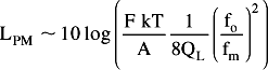 (4-27)
where LPM is single-sideband phase noise density (dBc/Hz), F is the device noise factor at operating power level A (linear), k is Boltzmann’s constant, 1.38 × 10⁻²³ J/K, T is temperature (K), A is oscillator output power (W), QL is loaded Q (dimensionless), fO is the oscillator carrier frequency, and fm is the frequency offset from the carrier.
For Leeson’s equation to be valid, the following must be true:
• fm, the offset frequency from the carrier, is greater than the 1/f;
Q includes the effects of component losses, device loading and buffer loading;
Leeson’s equation only applies in the knee region between the break (f1) to the transition from the “1/f” (more generally 1/fg) flicker noise frequency to a frequency beyond which amplified white noise dominates (f2). This is shown in Figure 4-60 (g = 3). f1 should be as low as possible; typically, it is less than 1 kHz, while f2 is in the region of a few MHz. High performance oscillators require devices specially selected for low 1/f transition frequency.
Some guidelines to minimizing the phase noise in VCOs are:
1. Keep the tuning voltage of the varactor sufficiently high (typically between 3 and 3.8 V).
2. Use filtering on the DC voltage supply.
3. Keep the inductor Q as high as possible. Typical off-the-shelf coils provide a Q of between 50 and 60.
4. Choose an active device that has minimal noise figure as well as low flicker frequency. The flicker noise can be reduced by the use of feedback elements.
5. Most active device exhibit a broad U-shaped noise figure versus bias-current curve. Use this information to choose the optimal operating bias current for the device.
6. Maximize the average power at the tank circuit output.
7. When buffering the VCO, use devices with the lowest possible noise figure.
Closing the Loop
Having looked at phase noise in a free-running VCO and how it can be minimized, we will now consider the effect of closing the loop on phase noise.
Figure 4-61 shows the main phase noise contributors in a PLL. The system transfer function may be described by the following equations.

For the discussion that follows, we will define SREF as the noise that appears on the reference input to the phase detector. It is dependent on the reference divider circuitry and the spectral purity of the main reference signal. SN is the noise due to the feedback divider appearing at the frequency input to the phase detector. SCP is the noise due to the phase detector (depending on its implementation). And SVCO is the phase noise of the VCO as described by equations developed earlier.
 (4-31)
The overall phase noise performance at the output depends on the terms described above. All the effects at the output are added in an RMS fashion to give the total noise of the system. Thus:
where STOT2 is the total phase noise power at the output, X2 is the noise power at the output due to SN and SREF, Y2 is the noise power at the output due to SCP, and Z2 is the noise power at the output due to SVCO.
The noise terms at the PD inputs, SREF and SN, will be operated on in the same fashion as FREF and will be multiplied by the CLG of the system.
 (4-33)
At low frequencies, inside the loop bandwidth,
and
At high frequencies, outside the loop bandwidth,
and
The overall output noise contribution due to the phase detector noise, SCP, can be calculated by referencing SCP back to the input of the PFD. The equivalent noise at the PD input is SCP/Kd. This is then multiplied by the CLG:
 (4-38)
Finally, the contribution of the VCO noise, SVCO, to the output phase noise is calculated in a similar manner. The forward gain this time is simply 1. Therefore its contribution to the output noise is:
 (4-39)
G, the forward loop gain of the closed-loop response, is usually a lowpass function; it is very large at low frequencies and small at high frequencies. H is a constant, 1/N. The denominator of the above expression is therefore lowpass, so SVCO is actually highpass filtered by the closed loop. A similar description of the noise contributors in a PLL/VCO can be found in Reference 1. Recall that the closed-loop response is a lowpass filter with a 3 dB cutoff frequency, BW, denoted the loop bandwidth. For frequency offsets at the output less than BW, the dominant terms in the output phase noise response are X and Y, the noise terms due to reference noise, N (counter noise), and CP noise.
Keeping SN and SREF to a minimum, keeping Kd large and keeping N small will thus minimize the phase noise inside the loop bandwidth, BW. Because N programs the output frequency, it is not generally available as a factor in noise reduction. For frequency offsets much greater than BW, the dominant noise term is that due to the VCO, SVCO. This is due to the highpass filtering of the VCO phase noise by the loop. A small value of BW would be desirable as it would minimize the total integrated output noise (phase error). However a small BW results in a slow transient response and increased contribution from the VCO phase noise inside the loop bandwidth. The loop bandwidth calculation therefore must tradeoff transient response and total output integrated phase noise.
To show the effect of closing the loop on a PLL, Figure 4-62 shows an overlay of the output of a free-running VCO and the output of a VCO as part of a PLL. Note that the in-band noise of the PLL has been attenuated compared to that of the free-running VCO.

Phase Noise Measurement
One of the most common ways of measuring phase noise is with a high frequency spectrum analyzer (Figure 4-64). Figure 4-65 is a typical example of what would be seen.


With the spectrum analyzer we can measure the spectral density of phase fluctuations per unit bandwidth. VCO phase noise is best described in the frequency domain where the spectral density is characterized by measuring the noise sidebands on either side of the output signal center frequency. Phase noise power is specified in decibels relative to the carrier (dBc/Hz) at a given frequency offset from the carrier. The following equation describes this single side band (SSB) phase noise (dBc/Hz).
The 10 MHz, 0 dBm reference oscillator, available on the spectrum analyzer’s rear-panel connector, has excellent phase noise performance. The R divider, N divider, and the phase detector are part of ADF4112 frequency synthesizer. These dividers are programmed serially under the control of a PC. The frequency and phase noise performance are observed on the spectrum analyzer.

Figure 4-65 illustrates a typical phase noise plot of a PLL synthesizer using an ADF4112 PLL with a Murata VCO, MQE520-1880. The frequency and phase noise were measured in a 5 kHz span. The reference frequency used was fREF = 200 kHz (R = 50) and the output frequency was 1880 MHz (N = 9400). If this were an ideal world PLL synthesizer, a single discrete tone would be displayed rising up above the spectrum analyzer’s noise floor. What is displayed here is the tone, with the phase noise due to the loop components. The loop filter values were chosen to give a loop bandwidth of approximately 20 kHz. The flat part of the phase noise for frequency offsets less than the loop bandwidth is actually the phase noise as described by X2 and Y2 in the section “closing the loop” for cases where f is inside the loop bandwidth. It is specified at a 1 kHz offset. The value measured, the phase noise power in a 1 Hz bandwidth, was 85.86 dBc/Hz. It is made up of the following:
1. Relative power in dBc between the carrier and the sideband noise at 1 kHz offset.
2. The spectrum analyzer displays the power for a certain resolution bandwidth (RBW). In the plot, a 10 Hz RBW is used. To represent this power in a 1 Hz bandwidth, 10log(RBW) must be subtracted from the value obtained from (1).
3. A correction factor, which takes into account the implementation of the RBW, the log display mode and detector characteristic, must be added to the result obtained in (2).
4. Phase noise measurement with the HP 8561E can be made quickly by using the marker noise function, MKR NOISE. This function takes into account the above three factors and displays the phase noise in dBc/Hz.
The phase noise measurement above is the total output phase noise at the VCO output. If we want to estimate the contribution of the PLL device (noise due to phase detector, R and N dividers, and the phase detector gain constant), the result must be divided by N2 (or 20 × log N be subtracted from the above result). This gives a phase noise floor of (–85.86 −20 × log(9400)) = −165.3 dBc/Hz.
Reference Spurs
In an integer-N PLL (where the output frequency is an integer multiple of the reference input), reference spurs are caused by the fact that the CP output is being continuously updated at the reference frequency rate. Consider again the basic model for the PLL. This is shown again in Figure 4-66.

When the PLL is in lock, the phase and frequency inputs to the PFD (fREF and fN) are essentially equal, and, in theory, one would expect that there to be no output from the PFD. However, this can create problems so the PFD is designed such that, in the locked condition, the current pulses from the CP will typically be as shown in Figure 4-67.

Although these pulses have a very narrow width, the fact that they exist means that the DC voltage driving the VCO is modulated by a signal of frequency fREF. This produces reference spurs in the RF output occurring at offset frequencies that are integer multiples of fREF. A spectrum analyzer can be used to detect reference spurs. Simply increase the span to greater than twice the reference frequency. A typical plot is shown in Figure 4-68.

In this case the reference frequency is 200 kHz and the diagram clearly shows reference spurs at ±200 kHz from the RF output of 1880 MHz. The level of these spurs is −90 dB. If the span were increased to more than 4 times the reference frequency, we would also see the spurs at (2 × fREF).
CP Leakage Current
When the CP output from the synthesizer is programmed to the high impedance state, there should, in theory, be no leakage current flowing. In practice, in some applications the level of leakage current will have an impact on overall system performance. For example, consider an application where a PLL is used in open-loop mode for FM—a simple and inexpensive way of implementing FM that also allows higher data rates than modulating in closed-loop mode. For FM, a closed-loop method works fine but the data rate is limited by the loop bandwidth.
A system that uses open-loop modulation is the European cordless telephone system, DECT. The output carrier frequencies are in a range of 1.77–1.90 GHz and the data rate is high, 1.152 Mbps.
A block diagram of open-loop modulation is shown in Figure 4-69. The principle of operation is as follows: The loop is initially closed to lock the RF output, fout = N fREF. The modulating signal is turned on and at first the modulation signal is simply the DC mean of the modulation. The loop is then opened, by putting the CP output of the synthesizer into high impedance mode, and the modulation data are fed to the Gaussian filter. The modulating voltage then appears at the VCO where it is multiplied by KV. When the data burst finishes, the loop is returned to the closed-loop mode of operation.
As the VCO usually has a high sensitivity (typical figures are between 20 and 80 MHz/V), any small voltage drift before the VCO will cause the output carrier frequency to drift. This voltage drift, and hence the system frequency drift, is directly dependent on the leakage current of the CP, when in the high impedance state. This leakage will cause the loop capacitor to charge or discharge depending on the polarity of the leakage current. For example, a leakage current of 1 nA would cause the voltage on the loop capacitor (1,000 pF for example) to charge or discharge by dV/dt = I/C (1 V/s in this case). This, in turn, would cause the VCO to drift. So, if the loop is open for 1 ms and the KV of the VCO is 50 MHz/V, the frequency drift caused by 1 nA leakage into a 1,000 pF loop capacitor would be 50 kHz. In fact, the DECT bursts are generally shorter (0.5 ms), so the drift will be even less in practice for the loop capacitance and leakage current used in the example. However, it does serve to illustrate the importance of charge pump leakage in this type of application.
1 Best R.E. Phase-Locked Loops. New York: McGraw-Hill, 1984.
2 Gardner F.M. Phaselock Techniques, 2nd Edition, New York: John Wiley, 1979.
3 Phase-Locked Loop Design Fundamentals, Applications Note AN-535, Motorola, Inc.
4 The ARRL Handbook for Radio Amateurs. Newington, CT: American Radio Relay League; 1992.
5 R.J. Kerr and L.A. Weaver, “Pseudorandom Dither for Frequency Synthesis Noise,” United States Patent Number 4,901,265, February 13, 1990.
6 H.T. Nicholas, III and H. Samueli, “An Analysis of the Output Spectrum of Direct Digital Frequency Synthesizers in the Presence of Phase-Accumulator Truncation,” IEEE 41st Annual Frequency Control Symposium Digest of Papers, 1987, pp. 495–502, IEEE Publication No. CH2427-3/87/0000-495.
7 H.T. Nicholas, III and H. Samueli, “The Optimization of Direct Digital Frequency Synthesizer Performance in the Presence of Finite Word Length Effects,” IEEE 42nd Annual Frequency Control Symposium Digest of Papers, 1988, pp. 357–363, IEEE Publication No. CH2588-2/88/0000-357.
8 Curtin M., O’Brien P. Phase-Locked Loops for High-Frequency Receivers and Transmitters-Part 1. Analog Dialogue. Vol. 33(3), 1999.
9 Curtin M., O’Brien P. Phase-Locked Loops for High-Frequency Receivers and Transmitters-Part 2. Analog Dialogue. Vol. 33(5), 1999.
10 Curtin M., O’Brien P. Phase Locked Loops for High-Frequency Receivers and Transmitters—Part 3. Analog Dialogue. Vol. 33(7), 1999.
11 VCO Designers’ Handbook. Mini-Circuits Corporation; 1996.
12 Couch L.W. Digital and Analog Communications Systems. New York: Macmillan Publishing Company, 1990.
13 Vizmuller P. RF Design Guide. Artech House, 1995.
14 Best R.L. Phase Locked Loops: Design, Simulation and Applications, 3rd Edition, New York: McGraw-Hill, 1997.
15 D.E. Fague, “Open Loop Modulation of VCOs for Cordless Telecommunications,” RF Design, 1994.
16 Leeson D.B. A Simplified Model of Feedback Oscillator Noise Spectrum. Proceedings of the IEEE. 1965;Vol. 42:329–330. February