
CHAPTER 3 Sensors
SECTION 3-1 Positional Sensors
Linear Variable Differential Transformers
The linear variable differential transformer (LVDT) is an accurate and reliable method for measuring linear distance. LVDTs find uses in modern machine-tool, robotics, avionics, and computerized manufacturing.
The LVDT (see Figure 3-1) is a position-to-electrical sensor whose output is proportional to the position of a movable magnetic core. The core moves linearly inside a transformer consisting of a center primary coil and two outer secondary coils wound on a cylindrical form. The primary winding is excited with an AC voltage source (typically several kHz), inducing secondary voltages which vary with the position of the magnetic core within the assembly. The core is usually threaded in order to facilitate attachment to a non-ferromagnetic rod which in turn is attached to the object whose movement or displacement is being measured.
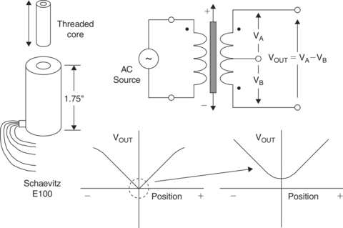
The secondary windings are wound out of phase with each other, and when the core is centered the voltages in the two secondary windings oppose each other, and the net output voltage is zero. When the core is moved off center, the voltage in the secondary toward which the core is moved increases, while the opposite voltage decreases. The result is a differential voltage output which varies linearly with the core’s position. Linearity is excellent over the design range of movement, typically 0.5% or better. The LVDT offers good accuracy, linearity, sensitivity, infinite resolution, as well as frictionless operation and ruggedness.
A wide variety of measurement ranges are available in different LVDTs, typically from ± 100 μm to ±25 cm. Typical excitation voltages range from 1 V to 24 VRMS, with frequencies from 50 Hz to 20 kHz. Note that a true null does not occur when the core is in center position because of mismatches between the two secondary windings and leakage inductance. Also, simply measuring the output voltage VOUT will not tell on which side of the null position the core resides.
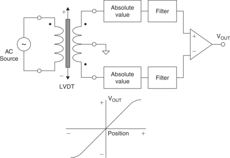
A signal conditioning circuit which removes these difficulties is shown in Figure 3-2 where the absolute values of the two output voltages are subtracted. Using this technique, both positive and negative variations about the center position can be measured. While a diode/capacitor-type rectifier could be used as the absolute value circuit, the precision rectifier shown in Figure 3-3 is more accurate and linear. The input is applied to a V/I converter which in turn drives an analog multiplier. The sign of the differential input is detected by the comparator whose output switches the sign of the V/I output via the analog multiplier. The final output is a precision replica of the absolute value of the input. These circuits are well-understood by integrated circuit (IC) designers and are easy to implement on modern bipolar processes.

The industry-standard AD598 LVDT signal conditioner shown in Figure 3-4 (simplified form) performs all required LVDT signal processing. The on-chip excitation frequency oscillator can be set from 20 Hz to 20 kHz with a single external capacitor. Two absolute value circuits followed by two filters are used to detect the amplitude of the A and B channel inputs. Analog circuits are then used to generate the ratiometric function (A − B)/(A + B). Note that this function is independent of the amplitude of the primary winding excitation voltage, assuming the sum of the LVDT output voltage amplitudes remains constant over the operating range. This is usually the case for most LVDTs, but the user should always check with the manufacturer if it is not specified on the LVDT data sheet. Note also that this approach requires the use of a five-wire LVDT.
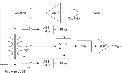
A single external resistor sets the AD598 excitation voltage from approximately 1 to 24 VRMS. Drive capability is 30 mARMS. The AD598 can drive an LVDT at the end of 300 feet of cable, since the circuit is not affected by phase shifts or absolute signal magnitudes. The position output range of VOUT is ± 11 V for a 6 mA load, and it can drive up to 1,000 feet of cable. The VA and VB inputs can be as low as 100 mVRMS.
The AD698 LVDT signal conditioner (see Figure 3-5) has similar specifications as the AD598 but processes the signals slightly differently and uses synchronous demodulation. The A and B signal processors each consist of an absolute value function and a filter. The A output is then divided by the B output to produce a final output which is ratiometric and independent of the excitation voltage amplitude. Note that the sum of the LVDT secondary voltages does not have to remain constant in the AD698.

The AD698 can also be used with a half-bridge (similar to an auto-transformer) LVDT as shown in Figure 3-6. In this arrangement, the entire secondary voltage is applied to the B processor, while the center-tap voltage is applied to the A processor. The half-bridge LVDT does not produce a null voltage, and the A/B ratio represents the range-of-travel of the core.

It should be noted that the LVDT concept can be implemented in rotary form, in which case the device is called a rotary variable differential transformer (RVDT). The shaft is equivalent to the core in an LVDT, and the transformer windings are wound on the stationary part of the assembly. However, the RVDT is linear over a relatively narrow range of rotation and is not capable of measuring a full 360° rotation. Although capable of continuous rotation, typical RVDTs are linear over a range of about ±40° about the null position (0°). Typical sensitivity is 2–3 mV/V/degree of rotation, with input voltages in the range of 3 VRMS at frequencies between 400 Hz and 20 kHz. The 0° position is marked on the shaft and the body.
Hall Effect Magnetic Sensors
If a current flows in a conductor (or semiconductor) and there is a magnetic field present which is perpendicular to the current flow, then the combination of current and magnetic field will generate a voltage perpendicular to both (see Figure 3-7). This phenomenon is called the Hall Effect, was discovered by E. H. Hall in 1879.

The voltage, VH, is known as the Hall Voltage. VH is a function of the current density, the magnetic field, and the charge density and carrier mobility of the conductor.
The Hall Effect may be used to measure magnetic fields (and hence in contact-free current measurement), but its commonest application is in motion sensors where a fixed Hall sensor and a small magnet attached to a moving part can replace a cam and contacts with a great improvement in reliability. (Cams wear and contacts arc become fouled, but magnets and Hall sensors can contact free and do neither.) Since VH is proportional to magnetic field and not to the rate of change of magnetic field like an inductive sensor, the Hall Effect provides a more reliable low speed sensor than an inductive pickup.
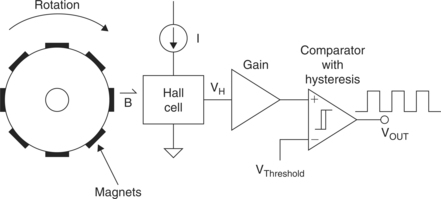
Although several materials can be used for Hall Effect sensors, silicon has the advantage that signal conditioning circuits can be integrated on the same chip as the sensor. Complementary-MOS (CMOS) processes are common for this application. A simple rotational speed detector can be made with a Hall sensor, a gain stage, and a comparator as shown in Figure 3-8. The circuit is designed to detect rotation speed as in automotive applications. It responds to small changes in field, and the comparator has built-in hysteresis to prevent oscillation. Several companies manufacture such Hall switches, and their usage is widespread.
There are many other applications, particularly in automotive throttle, pedal, suspension, and valve position sensing, where a linear representation of the magnetic field is desired. The AD22151 is a linear magnetic field sensor whose output voltage is proportional to a magnetic field applied perpendicularly to the package top surface (see Figure 3-9). The AD22151 combines integrated bulk Hall cell technology and conditioning circuitry to minimize temperature-related drifts associated with silicon Hall cell characteristics.

The architecture maximizes the advantages of a monolithic implementation while allowing sufficient versatility to meet varied application requirements with a minimum number of external components. Principal features include dynamic offset drift cancellation using a chopper-type op amp and a built-in temperature sensor. Designed for single +5 V supply operation, low offset, and gain drift allows operation over a −40°C to + 150°C range. Temperature compensation (set externally with a resistor R1) can accommodate a number of magnetic materials commonly utilized in position sensors. Output voltage range and gain can be easily set with external resistors. Typical gain range is usually set from 2 mV/G to 6 mV/G. Output voltage can be adjusted from fully bipolar (reversible) field operation to fully unipolar field sensing. The voltage output achieves near rail-to-rail dynamic range (+0.5 V to +4.5 V), capable of supplying 1 mA into large capacitive loads. The output signal is ratiometric to the positive supply rail in all configurations.
Resolvers and Synchros
Machine-tool and robotics manufacturers have increasingly turned to resolvers and synchros to provide accurate angular and rotational information. These devices excel in demanding factory applications requiring small size, long-term reliability, absolute position measurement, high accuracy, and low noise operation.
A diagram of a typical synchro and resolver is shown in Figure 3-10. Both synchros and resolvers employ single-winding rotors that revolve inside fixed stators. In the case of a simple synchro, the stator has three windings oriented 120° apart and electrically connected in a Y-connection. Resolvers differ from synchros in that their stators have only two windings oriented at 90°.

Because synchros have three stator coils in a 120° orientation, they are more difficult to manufacture than resolvers and are therefore more costly. Today, synchros find decreasing use, except in certain military and avionic retrofit applications.
Modern resolvers, in contrast, are available in a brushless form that employ a transformer to couple the rotor signals from the stator to the rotor. The primary winding of this transformer resides on the stator, and the secondary on the rotor. Other resolvers use more traditional brushes or slip rings to couple the signal into the rotor winding. Brushless resolvers are more rugged than synchros because there are no brushes to break or dislodge, and the life of a brushless resolver is limited only by its bearings. Most resolvers are specified to work over 2 V–40 VRMS and at frequencies from 400 Hz to 10 kHz. Angular accuracies range from 5 arc-minutes to 0.5 arc-minutes. (There are 60 arc-minutes in 1°, and 60 arc-seconds in 1 arc-minute. Hence, 1 arc-minute is equal to 0.0167°.)
In operation, synchros and resolvers resemble rotating transformers. The rotor winding is excited by an AC reference voltage, at frequencies up to a few kHz. The magnitude of the voltage induced in any stator winding is proportional to the sine of the angle (θ) between the rotor coil axis and the stator coil axis. In the case of a synchro, the voltage induced across any pair of stator terminals will be the vector sum of the voltages across the two connected coils.
For example, if the rotor of a synchro is excited with a reference voltage, V sin ωt, across its terminals R1 and R2, then the stator’s terminal will see voltages in the form:
where θ is the shaft angle.
In the case of a resolver, with a rotor AC reference voltage of V sin ωt, the stator’s terminal voltages will be:
It should be noted that the three-wire synchro output can be easily converted into the resolver-equivalent format using a Scott-T transformer. Therefore, the following signal processing example describes only the resolver configuration.
A typical resolver-to-digital converter (RDC) is shown functionally in Figure 3-11. The two outputs of the resolver are applied to cosine and sine multipliers. These multipliers incorporate sine and cosine lookup tables and function as multiplying digital-to-analog converters (DACs). Begin by assuming that the current state of the up/down counter is a digital number representing a trial angle, ϕ. The converter seeks to adjust the digital angle, ϕ, continuously to become equal to, and to track θ, the analog angle being measured. The resolver’s stator output voltages are written as:
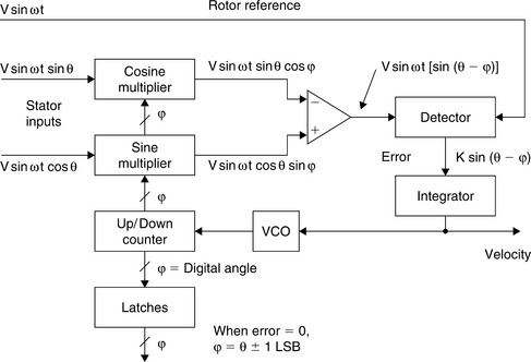
where θ is the angle of the resolver’s rotor. The digital angle ϕ is applied to the cosine multiplier, and its cosine is multiplied by V1 to produce the term:
The digital angle ϕ is also applied to the sine multiplier and multiplied by V2 to produce the term:
These two signals are subtracted from each other by the error amplifier to yield an AC error signal of the form:
Using a simple trigonometric identity, this reduces to:
The detector synchronously demodulates this AC error signal, using the resolver’s rotor voltage as a reference. This results in a DC error signal proportional to sin(θ – ϕ).
The DC error signal feeds an integrator, the output of which drives a voltage-controlled-oscillator (VCO). The VCO, in turn, causes the up/down counter to count in the proper direction to cause:
and therefore
to within one count. Hence, the counter’s digital output, ϕ, represents the angle θ. The latches enable this data to be transferred externally without interrupting the loop’s tracking.
Inductosyns
Synchros and resolvers inherently measure rotary position, but they can make linear position measurements when used with lead screws. An alternative, the Inductosyn™ (registered trademark of Farrand Controls, Inc.) measures linear position directly. In addition, Inductosyns are accurate and rugged, well-suited to severe industrial environments, and do not require ohmic contact.
The linear Inductosyn consists of two magnetically coupled parts; it resembles a multipole resolver in its operation (see Figure 3-12). One part, the scale, is fixed (e.g., with epoxy) to one axis, such as a machine-tool bed. The other part, the slider, moves along the scale in conjunction with the device to be positioned (e.g., the machine-tool carrier).

The scale is constructed of a base material such as steel, stainless steel, aluminum, or a tape of spring steel, covered by an insulating layer. Bonded to this is a printed circuit trace, in the form of a continuous rectangular waveform pattern. The pattern typically has a cyclic pitch of 0.1 inch, 0.2 inch, or 2 mm. The slider, about 4 inches long, has two separate but identical printed circuit traces bonded to the surface that faces the scale. These two traces have a waveform pattern with exactly the same cyclic pitch as the waveform on the scale, but one trace is shifted one-quarter of a cycle relative to the other. The slider and the scale remain separated by a small air gap of about 0.007 inch.
Inductosyn operation resembles that of a resolver. When the scale is energized with a sinewave, this voltage couples to the two slider windings, inducing voltages proportional to the sine and cosine of the slider’s spacing within the cyclic pitch of the scale. If S is the distance between pitches, and X is the slider displacement within a pitch, and the scale is energized with a voltage V sin ωt, then the slider windings will see terminal voltages of:
As the slider moves the distance of the scale pitch, the voltages produced by the two slider windings are similar to those produced by a resolver rotating through 360°. The absolute orientation of the Inductosyn is determined by counting successive pitches in either direction from an established starting point. Because the Inductosyn consists of a large number of cycles, some form of coarse control is necessary in order to avoid ambiguity. The usual method of providing this is to use a resolver or synchro operated through a rack and pinion or a lead screw.
In contrast to a resolver’s highly efficient transformation of 1:1 or 2:1, typical Inductosyns operate with transformation ratios of 100:1. This results in a pair of sinusoidal output signals in the millivolt range which generally require amplification.
Since the slider output signals are derived from an average of several spatial cycles, small errors in conductor spacing have minimal effects. This is an important reason for the Inductosyn’s very high accuracy. In combination with 12-bit RDCs, linear Inductosyns readily achieve 25 μ inch resolutions.
Rotary Inductosyns can be created by printing the scale on a circular rotor and the slider’s track pattern on a circular stator. Such rotary devices can achieve very high resolutions. For instance, a typical rotary Inductosyn may have 360 cyclic pitches per rotation, and might use a 12-bit RDC. The converter effectively divides each pitch into 4,096 sectors. Multiplying by 360 pitches, the rotary Inductosyn divides the circle into a total of 1,474,560 sectors. This corresponds to an angular resolution of less than 0.9 arc-seconds. As in the case of the linear Inductosyn, a means must be provided for counting the individual pitches as the shaft rotates. This may be done with an additional resolver acting as the coarse measurement.
Accelerometers
Accelerometers are widely used to measure tilt, inertial forces, shock, and vibration. They find wide usage in automotive, medical, industrial control, and other applications. Modern micromachining techniques allow these accelerometers to be manufactured on CMOS processes at low cost with high reliability. Analog Devices iMEMS® (integrated micro electro mechanical systems) accelerometers represent a breakthrough in this technology. A significant advantage of this type of accelerometer over piezoelectric-type charge-output accelerometers is that DC acceleration can be measured (e.g., they can be used in tilt measurements where the acceleration is a constant 1 g).
The basic unit cell sensor building block for these accelerometers is shown in Figure 3-13. The surface-micromachined sensor element is made by depositing polysilicon on a sacrificial oxide layer that is then etched away leaving the suspended sensor element. The actual sensor has tens of unit cells for sensing acceleration, but the diagram shows only one cell for clarity. The electrical basis of the sensor is the differential capacitor (CS1 and CS2) which is formed by a center plate which is part of the moving beam and two fixed outer plates. The two capacitors are equal at rest (no applied acceleration). When acceleration is applied, the mass of the beam causes it to move closer to one of the fixed plates while moving further from the other. This change in differential capacitance forms the electrical basis for the conditioning electronics as shown in Figure 3-14.


The sensor’s fixed capacitor plates are driven differentially by a 1 MHz square wave: the two square wave amplitudes are equal but are 180° out of phase. When at rest, the values of the two capacitors are the same, and therefore the voltage output at their electrical center (i.e., at the center plate attached to the movable beam) is zero. When the beam begins to move, a mismatch in the capacitance produces an output signal at the center plate. The output amplitude will increase with the acceleration experienced by the sensor. The center plate is buffered by A1 and applied to a synchronous demodulator. The direction of beam motion affects the phase of the signal, and synchronous demodulation is therefore used to extract the amplitude information. The synchronous demodulator output is amplified by A2 which supplies the acceleration output voltage, VOUT.
An interesting application of low-g accelerometers is measuring tilt. Figure 3-15 shows the response of an accelerometer to tilt. The accelerometer output on the diagram has been normalized to 1 g full-scale. The accelerometer output is proportional to the sine of the tilt angle with respect to the horizon. Note that maximum sensitivity occurs when the accelerometer axis is perpendicular to the acceleration. This scheme allows tilt angles from −90° to + 90° (180° of rotation) to be measured. However, in order to measure a full 360° rotation, a dual axis accelerometer must be used.

Figure 3-16 shows a simplified block diagram of the ADXL202 dual axis ±2 g accelerometer. The output is a pulse whose duty cycle contains the acceleration information. This type of output is extremely useful because of its high noise immunity, and the data are transmitted over a single wire. Standard low cost microcontrollers have timers which can be easily used to measure the T1 and T2 intervals. The acceleration in g is then calculated using the formula:

Note that a duty cycle of 50% (T1 = T2) yields a 0 g output. T2 does not have to be measured for every measurement cycle. It need only be updated to account for changes due to temperature. Since the T2 time period is shared by both X and Y channels, it is necessary to measure it on only one channel. The T2 period can be set from 0.5 ms to 10 ms with an external resistor.
Analog voltages representing acceleration can be obtained by buffering the signal from the XFILT and YFILT outputs or by passing the duty cycle signal through an RC filter to reconstruct its DC value.
A single accelerometer cannot work in all applications. Specifically, there is a need for both low-g and high-g accelerometers. Low-g devices are useful in such applications as tilt measurements, but higher-g accelerometers are needed in applications such as airbag crash sensors.
iMEMS® Angular-Rate-Sensing Gyroscope
The ADXRS150 and ADXRS300 gyros, with full-scale ranges of 150°/seconds and 300°/seconds, represent a quantum jump in gyro technology. The first commercially available surface-micromachined angular-rate sensors with integrated electronics, are smaller—with lower power consumption, and better immunity to shock and vibration—than any gyros having comparable functionality.
Gyroscope Description
Gyroscopes are used to measure angular rate—how quickly an object turns. The rotation is typically measured in reference to one of three axes: yaw, pitch, or roll. Figure 3-17 shows a diagram representing each axis of sensitivity relative to a package mounted to a flat surface. Depending on how a gyro normally sits, its primary axis of sensitivity can be one of the three axes of motion: yaw, pitch, or roll. The ADXRS150 and ADXRS300 are yaw-axis gyros, but they can measure rotation about other axes by appropriate mounting orientation. For example, at the right of Figure 3-17 a yaw-axis device is positioned to measure roll.

A gyroscope with one axis of sensitivity can also be used to measure other axes by mounting the gyro differently, as shown in the right-hand diagram. Here, a yaw-axis gyro, such as the ADXRS150 or ADXRS300, is mounted on its side so that the yaw-axis becomes the roll axis.
As an example of how a gyro could be used, a yaw-axis gyro mounted on a turntable rotating at 33 1/3 rpm (revolutions per minute) would measure a constant rotation of 360° times 33 1/3 rpm divided by 60 seconds, or 200°/seconds. The gyro would output a voltage proportional to the angular rate, as determined by its sensitivity, measured in millivolts per degree per second (mV/°/s). The full-scale voltage determines how much angular rate can be measured, so in the example of the turntable, a gyro would need to have a full-scale voltage corresponding to at least 200°/seconds. Full-scale is limited by the available voltage swing divided by the sensitivity. The ADXRS300, for example, with 1.5 V full-scale and a sensitivity of 5 mV/°/seconds, handles a full-scale of 300°/seconds. The ADXRS150, has a more limited full-scale of 150°/seconds but a greater sensitivity of 12.5 mV/°/seconds.
One practical application is to measure how quickly a car turns by mounting a gyro inside the vehicle; if the gyro senses that the car is spinning out of control, differential braking engages to bring it back into control. The angular rate can also be integrated over time to determine angular position—particularly useful for maintaining continuity of GPS-based navigation when the satellite signal is lost for short periods of time.
Coriolis Acceleration
Analog Devices’ (ADI) ADXRS gyros measure angular rate by means of Coriolis acceleration. The Coriolis effect can be explained as follows, starting with Figure 3-18. Consider yourself standing on a rotating platform, near the center. Your speed relative to the ground is shown as the arrow lengths in Figure 3-18. If you were to move to a point near the outer edge of the platform, your speed would increase relative to the ground, as indicated by the longer arrow. The rate of increase of your tangential speed, caused by your radial velocity, is the Coriolis acceleration (after Gaspard G. de Coriolis, 1792–1843—a French mathematician).

If Ω is the angular rate and r the radius, the tangential velocity is Ωr. So, if r changes at speed, v, there will be a tangential acceleration Ωv. This is half of the Coriolis acceleration. There is another half from changing the direction of the radial velocity giving a total of 2 Ωv. If you have mass, M, the platform must apply a force, 2 MΩv, to cause that acceleration, and the mass experiences a corresponding reaction force.
Motion in two dimensions
Consider the position coordinate, z = rεiθ, in the complex plane. Differentiating with respect to time, t, the velocity is:
The two terms are the respective radial and tangential components, the latter arising from the angular rate. Differentiating again, the acceleration is:
 (3-19)
The first term is the radial linear acceleration and the fourth term is the tangential component arising from angular acceleration. The last term is the familiar centripetal acceleration needed to constrain r. The second and third terms are tangential and are the Coriolis acceleration components. They are equal, respectively arising from the changing direction of the radial velocity and from the changing magnitude of the tangential velocity. If the angular rate and radial velocities are constant,
and
where the angular component, iεiθ, indicates a tangential direction in the sense of positive θ for the Coriolis acceleration, 2 Ωv, and −εiθ indicates toward the center (i.e., centripetal) for the Ω2r component.
The ADXRS gyros take advantage of this effect by using a resonating mass analogous to the person moving out and in on a rotating platform. The mass is micromachined from polysilicon and is tethered to a polysilicon frame so that it can resonate along only one direction.
Figure 3-19 shows that when the resonating mass moves toward the outer edge of the rotation, it is accelerated to the right and exerts on the frame a reaction force to the left. When it moves toward the center of the rotation, it exerts a force to the right, as indicated by the arrows.

To measure the Coriolis acceleration, the frame containing the resonating mass is tethered to the substrate by springs at 90° relative to the resonating motion, as shown in Figure 3-20. This figure also shows the Coriolis sense fingers that are used to capacitively sense displacement of the frame in response to the force exerted by the mass, as described in Figure 3-19, a demonstration of the Coriolis effect in response to a resonating silicon mass suspended inside a frame. The arrows indicate the force applied to the structure, based on the status of the resonating mass.

In Figure 3-21 the frame and resonating mass are displaced laterally in response to the Coriolis effect. The displacement is determined from the change in capacitance between the Coriolis sense fingers on the frame and those attached to the substrate.
If the springs have a stiffness, K, then the displacement resulting from the reaction force will be 2 ΩνM/K.
Figure 3-21, which shows the complete structure, demonstrates that as the resonating mass moves, and as the surface to which the gyro is mounted rotates, the mass and its frame experience the Coriolis acceleration and are translated 90° from the vibratory movement. As the rate of rotation increases, so does the displacement of the mass and the signal derived from the corresponding capacitance change.
It should be noted that the gyro may be placed anywhere on the rotating object and at any angle, as long as its sensing axis is parallel to the axis of rotation. The above explanation is intended to give an intuitive sense of the function and has been simplified by the placement of the gyro.
Capacitive Sensing
ADXRS gyros measure the displacement of the resonating mass and its frame due to the Coriolis effect through capacitive sensing elements attached to the resonator, as shown in Figures 3-19, 20, and 21. These elements are silicon beams inter-digitated with two sets of stationary silicon beams attached to the substrate, thus forming two nominally equal capacitors. Displacement due to angular rate induces a differential capacitance in this system. If the total capacitance is C and the spacing of the beams is g, then the differential capacitance is 2 ΩvMC/gK, and is directly proportional to the angular rate. The fidelity of this relationship is excellent in practice, with nonlinearity less than 0.1%.
The ADXRS gyro electronics can resolve capacitance changes as small as 12 × 10−21F (12 zF) from beam deflections as small as 0.00016 Å (16 fm). The only way this can be utilized in a practical device is by situating the electronics, including amplifiers and filters, on the same die as the mechanical sensor. The differential signal alternates at the resonator frequency and can be extracted from the noise by correlation.
These sub-atomic displacements are meaningful as the average positions of the surfaces of the beams, even though the individual atoms on the surface are moving randomly by much more. There are about 1,012 atoms on the surfaces of the capacitors, so the statistical averaging of their individual motions reduces the uncertainty by a factor of 106. So why can’t we do 100 times better? The answer is that the impact of the air molecules causes the structure to move—although similarly averaged, their effect is far greater! So why not remove the air? The device is not operated in a vacuum because it is a very fine, thin film weighing only 4 μg; its flexures, only 1.7 μ wide, are suspended over the silicon substrate. Air cushions the structure, preventing it from being destroyed by violent shocks—even those experienced during firing of a guided shell from a howitzer (as demonstrated recently).
Figure 3-22 shows that the ADXRS gyros include two structures to enable differential sensing in order to reject environmental shock and vibration.

Integration of electronics and mechanical elements is a key feature of products such as the ADXRS150 and ADXRS300, because it makes possible the smallest size and cost for a given performance level. Figure 3-23 is a photograph of the ADXRS die, highlighting the integration of the mechanical rate sensor and the signal conditioning electronics.

The ADXRS150 and ADXRS300 are housed in an industry-standard package that simplifies users’ product development and production. The ceramic package—a 32-pin ball grid array (BGA)—measures 7 mm wide by 7 mm deep by 3 mm tall. It is at least 100 times smaller than any other gyro having similar performance. Besides their small size, these gyros consume 30 mW, far less power than similar gyros. The combination of small size and low power make these products ideally suited for consumer applications such as toy robots, scooters, and navigation devices.
Immunity to Shock and Vibration
One of the most important concerns for a gyro user is the device’s ability to reliably provide an accurate angular-rate output signal—even in the presence of environmental shock and vibration. One example of such an application is automotive rollover detection, in which a gyro is used to detect whether or not a car (or SUV) is rolling over. Some rollover events are triggered by an impact with another object, such as a curb, that results in a shock to the vehicle. If the shock saturates the gyro sensor, and the gyro cannot filter it out, then the airbags may not deploy. Similarly, if a bump in the road results in a shock or vibration that translates into a rotational signal, the airbags might deploy when not needed—a considerable safety hazard!
As can be seen, the ADXRS gyros employ a novel approach to angular-rate sensing that makes it possible to reject shocks of up to 1,000 g—they use two resonators to differentially sense signals and reject common-mode external accelerations that are unrelated to angular motion. This approach is, in part, the reason for the excellent immunity of the ADXRS gyros to shock and vibration. The two resonators in Figure 3-22 are mechanically independent, and they operate antiphase. As a result, they measure the same magnitude of rotation, but give outputs in opposite directions. Therefore, the difference between the two sensor signals is used to measure angular rate. This cancels non-rotational signals that affect both sensors. The signals are combined in the internal hard-wiring ahead of the very sensitive preamplifiers. Thus, extreme acceleration overloads are largely prevented from reaching the electronics—thereby allowing the signal conditioning to preserve the angular-rate output during large shocks. This scheme requires that the two sensors be well-matched, precisely fabricated copies of each other.
References: Positional Sensors
1 Schaevitz H. The Linear Variable Differential Transformer. Proceedings of the SASE. Vol. 4(2), 1946.
2 Dr. E.D.D. Schmidt, “Linear Displacement—Linear Variable Differential Transformers – LVDTs,” Schaevitz Sensors, http://www.schaevitz.com.
3 E-Series LVDT Data Sheet, Schaevitz Sensors, http://www.schaevitz.com. Schaevitz Sensors is now a division of Lucas Control Systems, 1000 Lucas Way, Hampton, VA 23666.
4 Pallas-Areny R., Webster J.G. Sensors and Signal Conditioning. New York: John Wiley, 1991.
5 Trietley H.L. Transducers in Mechanical and Electronic Design. Inc.: Marcel Dekker, 1986.
6 AD598 and AD698 Data Sheet, Analog Devices, Inc., http://www.analog.com.
7 Travis B. Hall-Effect Sensor ICs Sport Magnetic Personalities. EDN. 1998;Vol. XX:81–91. April 9
8 AD22151 Data Sheet, Analog Devices, Inc., http://www.analog.com
9 Sheingold D. Analog-Digital Conversion Handbook, 3rd Edition, Norwood, MA: Prentice-Hall, 1986.
10 F.P. Flett, “Vector Control Using a Single Vector Rotation Semiconductor for Induction and Permanent Magnet Motors,” PCIM Conference, Intelligent Motion, September 1992 Proceedings, Available from Analog Devices.
11 F.P. Flett, “Silicon Control Algorithms for Brushless Permanent Magnet Synchronous Machines,” PCIM Conference, Intelligent Motion, June 1991 Proceedings, Available from Analog Devices.
12 P.J.M. Coussens, et al., “Three Phase Measurements with Vector Rotation Blocks in Mains and Motion Control,” PCIM Conference, Intelligent Motion, April 1992 Proceedings, Available from Analog Devices.
13 Dennis Fu, “Digital to Synchro and Resolver Conversion with the AC Vector Processor AD2S100,” Available from Analog Devices.
14 Dennis Fu, “Circuit Applications of the AD2S90 Resolver-to-Digital Converter, AN-230,” Analog Devices.
15 A. Murray and P. Kettle, “Towards a Single Chip DSP Based Motor Control Solution,” Proceedings PCIM—Intelligent Motion, May 1996, Nurnberg, Germany, pp. 315–326. Also available at http://www.analog.com.
16 D.J. Lucey, P.J. Roche, M.B. Harrington, and J.R. Scannell, “Comparison of Various Space Vector Modulation Strategies,” Proceedings Irish DSP and Control Colloquium, July 1994, Dublin, Ireland, pp. 169–175.
17 N. Lyne, “ADCs Lend Flexibility to Vector Motor Control Application,” Electronic Design, May 1, 1998, pp. 93–100.
18 F. Goodenough, “Airbags Boom when IC Accelerometer Sees 50 g,” Electronic Design, 1991.
SECTION 3-2 Temperature Sensors
Introduction
Measurement of temperature is critical in modern electronic devices, especially expensive laptop computers and other portable devices with densely packed circuits which dissipate considerable power in the form of heat. Knowledge of system temperature can also be used to control battery charging as well as prevent damage to expensive microprocessors.
Compact high power portable equipment often has fan cooling to maintain junction temperatures at proper levels. In order to conserve battery life, the fan should only operate when necessary. Accurate control of the fan requires a knowledge of critical temperatures from the appropriate temperature sensor.
Accurate temperature measurements are required in many other measurement systems such as process control and instrumentation applications. In most cases, because of low level nonlinear outputs, the sensor output must be properly conditioned and amplified before further processing can occur.
Except for IC sensors, all temperature sensors have nonlinear transfer functions. In the past, complex analog conditioning circuits were designed to correct for the sensor nonlinearity. These circuits often required manual calibration and precision resistors to achieve the desired accuracy. Today, however, sensor outputs may be digitized directly by high resolution analog-to-digital converters (ADCs). Linearization and calibration is then performed digitally, thereby reducing cost and complexity.
Resistance Temperature Detectors (RTDs) are accurate, but require excitation current and are generally used in bridge circuits. Thermistors have the most sensitivity but are the most nonlinear. However, they are popular in portable applications such as measurement of battery temperature and other critical temperatures in a system.
Modern semiconductor temperature sensors offer high accuracy and high linearity over an operating range of about −55°C to + 150°C. Internal amplifiers can scale the output to convenient values, such as 10 mV/°C. They are also useful in cold-junction compensation circuits for wide temperature range thermocouples. Semiconductor temperature sensors can be integrated into multi-function ICs which perform a number of other hardware monitoring functions.
Figure 3-24 lists the most popular types of temperature transducers and their characteristics.

Semiconductor Temperature Sensors
Modern semiconductor temperature sensors offer high accuracy and high linearity over an operating range of about −55°C to + 150°C. Internal amplifiers can scale the output to convenient values, such as 10 mV/°C. They are also useful in cold-junction compensation circuits for wide temperature range thermocouples.
All semiconductor temperature sensors make use of the relationship between a bipolar junction transistor’s (BJT) base-emitter voltage to its collector current:
 (3-23)
where k is Boltzmann’s constant, T is the absolute temperature, q is the charge of an electron, and Is is a current related to the geometry and the temperature of the transistors. (The equation assumes a voltage of at least a few hundred mV on the collector, and ignores early effects.)
If we take N transistors identical to the first (see Figure 3-25) and allow the total current Ic to be shared equally among them, we find that the new base-emitter voltage is given by the equation

 (3-24)
Neither of these circuits is of much use by itself because of the strongly temperature dependent current Is, but if we have equal currents in one BJT and N similar BJTs then the expression for the difference between the two base-emitter voltages is proportional to absolute temperature (PTAT) and does not contain Is.
 (3-25)
 (3-26)
 (3-27)
The circuit shown in Figure 3-26 implements the above equation and is known as the “Brokaw Cell” (see Reference 10). The voltage ΔVBE = VBE −VN appears across resistor R2. The emitter current in Q2 is therefore ΔVBE/R2. The op amp’s servo loop and the resistors, R, force the same current to flow through Q1. The Q1 and Q2 currents are equal and are summed and flow into resistor R1. The corresponding voltage developed across R1 is PTAT and given by:

The bandgap cell reference voltage, VBANDGAP, appears at the base of Q1 and is the sum of VBE(Q1) and VPTAT. VBE(Q1) is complementary to absolute temperature (CTAT), and summing it with VPTAT causes the bandgap voltage to be constant with respect to temperature (assuming proper choice of R1/R2 ratio and N to make the bandgap voltage equal to 1.205 V). This circuit is the basic bandgap temperature sensor and is widely used in semiconductor temperature sensors.
Current Out Temperature Sensors
This type of temperature sensor produces a current output PTAT. For supply voltages between 4 V and 30 V the device acts as a high impedance constant current regulator with an output PTAT with a typical transfer function of 1 μA/°K. This means that at 25°C there will be 298 μA flowing in the loop.
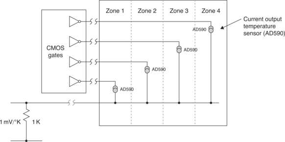
A current output temperature sensor such as the AD590 is particularly useful in remote sensing applications. These devices are insensitive to voltage drops over long lines due to their high impedance current outputs. The output characteristics also make this type of device easy to multiplex: the current can be switched by a simple logic gate as shown in Figure 3-27.
Current and Voltage Output Temperature Sensors
The concepts used in the bandgap temperature sensor discussion above can be used as the basis for a variety of IC temperature sensors to generate either current or voltage outputs.
In some cases, it is desirable for the output of a temperature sensor to be ratiometric with its supply voltage. The AD22100 (see Figure 3-28) has an output that is ratiometric with its supply voltage (nominally 5 V) according to the equation:

The circuit shown in Figure 3-28 uses the AD22100 power supply as the reference to the ADC, thereby eliminating the need for a precision voltage reference.
The thermal time constant of a temperature sensor is defined to be the time required for the sensor to reach 63.2% of the final value for a step change in the temperature. Figure 3-29 shows the thermal time constant of the ADT45/ADT50 series of sensors with the SOT-23-3 package soldered to 0.338″ × 0.307″ copper PC board as a function of air flow velocity. Note the rapid drop from 32 seconds to 12 seconds as the air velocity increases from 0 (still air) to 100 LFPM. As a point of reference, the thermal time constant of the ADT45/ADT50 series in a stirred oil bath is less than 1 second, which verifies that the major part of the thermal time constant is determined by the case.

The power supply pin of these sensors should be bypassed to ground with a 0.1 μF ceramic capacitor having very short leads (preferably surface mount) and located as close to the power supply pin as possible.
Since these temperature sensors operate on very little supply current and could be exposed to very hostile electrical environments, it is important to minimize the effects of electromagnetic interference (EMI)/radio frequency interference (RFI) on these devices. The effect of RFI on these temperature sensors is manifested as abnormal DC shifts in the output voltage due to rectification of the high frequency noise by the internal IC junctions. In those cases where the devices are operated in the presence of high frequency radiated or conducted noise, a large value tantalum electrolytic capacitor (>2.2 μF) placed across the 0.1 μF ceramic may offer additional noise immunity.
Thermocouple Principles and Cold-Junction Compensation
Thermocouples are small, rugged, relatively inexpensive, and operate over the widest range of all temperature sensors. They are especially useful for making measurements at extremely high temperatures (up to +2300°C) in hostile environments. They produce only millivolts of output, however, and require precision amplification for further processing. They also require cold-junction compensation (CJC) techniques which will be discussed shortly. They are more linear than many other sensors, and their nonlinearity has been well-characterized. Some common thermocouples are shown in Figure 3-30. The most common metals used are Iron, Platinum, Rhodium, Rhenium, Tungsten, Copper, Alumel (composed of Nickel and Aluminum), Chromel (composed of Nickel and Chromium), and Constantan (composed of Copper and Nickel).
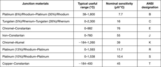
Figure 3-31 shows the voltage-temperature curves of three commonly used thermocouples, referred to a 0°C fixed-temperature reference junction. Of the thermocouples shown, Type J thermocouples are the most sensitive, producing the largest output voltage for a given temperature change. On the other hand, Type S thermocouples are the least sensitive. These characteristics are very important to consider when designing signal conditioning circuitry in that the thermocouples’ relatively low output signals require low noise, low-drift, high gain amplifiers.

To understand thermocouple behavior, it is necessary to consider the nonlinearities in their response to temperature differences. Figure 3-31 shows the relationships between sensing junction temperature and voltage output for a number of thermocouple types (in all cases, the reference cold junction is maintained at 0°C). It is evident that the responses are not quite linear, but the nature of the nonlinearity is not so obvious.
Figure 3-32 shows how the Seebeck coefficient (the change of output voltage with change of sensor junction temperature—i.e., the first derivative of output with respect to temperature) varies with sensor junction temperature (we are still considering the case where the reference junction is maintained at 0°C).

When selecting a thermocouple for making measurements over a particular range of temperature, we should choose a thermocouple whose Seebeck coefficient varies as little as possible over that range.
For example, a Type J thermocouple has a Seebeck coefficient which varies by less than 1 μV/°C between 200 and 500°C, which makes it ideal for measurements in this range.
Presenting these data on thermocouples serves two purposes. First, Figure 3-30 illustrates the range and sensitivity of the three thermocouple types so that the system designer can, at a glance, determine that a Type S thermocouple has the widest useful temperature range, but a Type J thermocouple is more sensitive. Second, the Seebeck coefficients provide a quick guide to a thermocouple’s linearity. Using Figure 3-31 the system designer can choose a Type K thermocouple for its linear Seebeck coefficient over the range of 400°C−800°C or a Type S over the range of 900°C–1,700°C. The behavior of a thermocouple’s Seebeck coefficient is important in applications where variations of temperature rather than absolute magnitude are important. These data also indicate what performance is required of the associated signal conditioning circuitry.
To use thermocouples successfully we must understand their basic principles. Consider the diagrams in Figure 3-33.

If we join two dissimilar metals at any temperature above absolute zero, there will be a potential difference between them (their “thermoelectric e.m.f.” or “contact potential”) which is a function of the temperature of the junction (Figure 3-33(A)). If we join the two wires at two places, two junctions are formed (Figure 3-33(B)). If the two junctions are at different temperatures, there will be a net e.m.f. in the circuit, and a current will flow determined by the e.m.f. and the total resistance in the circuit (Figure 3-33(B)). If we break one of the wires, the voltage across the break will be equal to the net thermoelectric e.m.f. of the circuit, and if we measure this voltage, we can use it to calculate the temperature difference between the two junctions (Figure 3-33(C)). We must always remember that a thermocouple measures the temperature difference between two junctions, not the absolute temperature at one junction. We can only measure the temperature at the measuring junction if we know the temperature of the other junction (often called the “reference” junction or the “cold” junction).
But it is not so easy to measure the voltage generated by a thermocouple. Suppose that we attach a voltmeter to the circuit in Figure 3-33(C) (Figure 3-33(D)). The wires attached to the voltmeter will form further thermojunctions where they are attached. If both these additional junctions are at the same temperature (it does not matter what temperature), then the “Law of Intermediate Metals” states that they will make no net contribution to the total e.m.f. of the system. If they are at different temperatures, they will introduce errors. Since every pair of dissimilar metals in contact generates a thermoelectric e.m.f. (including copper/solder, kovar/copper (kovar is the alloy used for IC leadframes) and aluminum/kovar (at the bond inside the IC)), it is obvious that in practical circuits the problem is even more complex, and it is necessary to take extreme care to ensure that all the junction pairs in the circuitry around a thermocouple, except the measurement and reference junctions themselves, are at the same temperature.
Thermocouples generate a voltage, albeit a very small one, and do not require excitation. As shown in Figure 3-33(D), however, two junctions (T1, the measurement junction and T2, the reference junction) are involved. If T2 = T1, then V2 = V1, and the output voltage V = 0. Thermocouple output voltages are often defined with a reference junction temperature of 0°C (hence the term cold or ice-point junction), so the thermocouple provides an output voltage of 0 V at 0°C. To maintain system accuracy, the reference junction must therefore be at a well-defined temperature (but not necessarily 0°C). A conceptually simple approach to this need is shown in Figure 3-34. Although an ice/water bath is relatively easy to define, it is quite inconvenient to maintain.
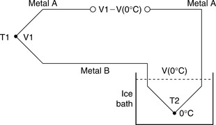
Today an ice-point reference, and its inconvenient ice/water bath, is generally replaced by electronics. A temperature sensor of another sort (often a semiconductor sensor, sometimes a thermistor) measures the temperature of the cold junction and is used to inject a voltage into the thermocouple circuit which compensates for the difference between the actual cold-junction temperature and its ideal value (usually 0°C) as shown in Figure 3-35. Ideally, the compensation voltage should be an exact match for the difference voltage required, which is why the diagram gives the voltage as f(T2) (a function of T2) rather than KT2, where K is a simple constant. In practice, since the cold junction is rarely more than a few tens of degrees from 0°C, and generally varies by little more than ± 10°C, a linear approximation (V = KT2) to the more complex reality is sufficiently accurate and is what is often used. (The expression for the output voltage of a thermocouple with its measuring junction at T°C and its reference at 0°C is a polynomial of the form V = K1T + K2T2 + K3T3 + …, but the values of the coefficients K2, K3, etc. are very small for most common types of thermocouple. References 8 and 9 give the values of these coefficients for a wide range of thermocouples.)

When electronic cold-junction compensation is used, it is common practice to eliminate the additional thermocouple wire and terminate the thermocouple leads in the isothermal block in the arrangement shown in Figure 3-36. The metal A (copper) and the metal B (copper) junctions, if at the same temperature, are equivalent to the metal A–metal B thermocouple junctions in Figure 3-35.

The circuit in Figure 3-37 conditions the output of a Type K thermocouple, while providing cold-junction compensation, for temperatures between 0°C and 250°C. The circuit operates from single +3.3 V to + 12 V supplies and has been designed to produce an output voltage transfer characteristic of 10 mV/°C.

A Type K thermocouple exhibits a Seebeck coefficient of approximately 41 μV/°C; therefore, at the cold junction, the TMP35 voltage output sensor with a temperature coefficient (TC) of 10 mV/°C is used with R1 and R2 to introduce an opposing cold-junction TC of −41 μV/°C. This prevents the isothermal, cold-junction connection between the circuit’s printed circuit board traces and the thermocouple’s wires from introducing an error in the measured temperature. This compensation works extremely well for circuit ambient temperatures in the range of 20–50°C. Over a 250°C measurement temperature range, the thermocouple produces an output voltage change of 10.151 mV. Since the required circuit’s output full-scale voltage change is 2.5 V, the gain of the circuit is set to 246.3. Choosing R4 equal to 4.99 kΩ sets R5 equal to 1.22 MΩ. Since the closest 1% value for R5 is 1.21 MΩ, a 50 kΩ potentiometer is used with R5 for fine trim of the full-scale output voltage. Although the OP193 is a single-supply op amp, its output stage is not rail-to-rail, and will only go down to about 0.1 V above ground. For this reason, R3 is added to the circuit to supply an output offset voltage of about 0.1 V for a nominal supply voltage of 5 V. This offset (10°C) must be subtracted when making measurements referenced to the OP193 output. R3 also provides an open thermocouple detection, forcing the output voltage to greater than 3 V should the thermocouple open. Resistor R7 balances the DC input impedance of the OP193, and the 0.1 μF film capacitor reduces noise coupling into its non-inverting input.
The AD594/AD595 is a complete instrumentation amplifier and thermocouple cold-junction compensator on a monolithic chip (see Figure 3-38). It combines an ice-point reference with a precalibrated amplifier to provide a high level (10 mV/°C) output directly from the thermocouple signal. Pin-strapping options allow it to be used as a linear amplifier–compensator or as a switched output setpoint controller using either fixed or remote setpoint control. It can be used to amplify its compensation voltage directly, thereby becoming a stand-alone Celsius transducer with 10 mV/°C output. In such applications it is very important that the IC chip is at the same temperature as the cold junction of the thermocouple, which is usually achieved by keeping the two in close proximity and isolated from any heat sources.

The AD594/AD595 includes a thermocouple failure alarm that indicates if one or both thermocouple leads open. The alarm output has a flexible format which includes TTL drive capability. The device can be powered from a single-ended supply (which may be as low as +5 V), but by including a negative supply, temperatures below 0°C can be measured. To minimize self-heating, an unloaded AD594/AD595 will operate with a supply current of 160 μA, but is also capable of delivering ± 5 mA to a load.
The AD594 is precalibrated by laser wafer trimming to match the characteristics of type J (iron/constantan) thermocouples, and the AD595 is laser trimmed for type K (chromel/alumel). The temperature transducer voltages and gain control resistors are available at the package pins so that the circuit can be recalibrated for other thermocouple types by the addition of resistors. These terminals also allow more precise calibration for both thermocouple and thermometer applications. The AD594/AD595 is available in two performance grades. The C and the A versions have calibration accuracies of ± 1°C and ± 3°C, respectively. Both are designed to be used with cold junctions between 0°C and + 50°C. The circuit shown in Figure 3-38 will provide a direct output from a type J thermocouple (AD594) or a type K thermocouple (AD595) capable of measuring 0 to +300°C.
The AD596/AD597 are monolithic setpoint controllers which have been optimized for use at elevated temperatures as are found in oven control applications. The device cold-junction compensates and amplifies a type J/K thermocouple to derive an internal signal proportional to temperature. They can be configured to provide a voltage output (10 mV/°C) directly from type J/K thermocouple signals. The device is packaged in a 10-pin metal can and is trimmed to operate over an ambient range from +25°C to + 100°C. The AD596 will amplify thermocouple signals covering the entire −200°C to + 760°C temperature range recommended for type J thermocouples while the AD597 can accommodate −200°C to + 1,250°C type K inputs. They have a calibration accuracy of ± 4°C at an ambient temperature of 60°C and an ambient temperature stability specification of 0.05°C/°C from +25°C to +100°C.
None of the thermocouple amplifiers previously described compensates for thermocouple nonlinearity; they only provide conditioning and voltage gain. High resolution ADCs such as the AD77XX family can be used to digitize the thermocouple output directly, allowing a microcontroller to perform the transfer function linearization as shown in Figure 3-39. The two multiplexed inputs to the ADC are used to digitize the thermocouple voltage and the cold-junction temperature sensor outputs directly. The input programmable gain amplifier (PGA) gain is programmable from 1 to 128, and the ADC resolution is between 16 and 22 bits (depending on the particular ADC selected). The microcontroller performs both the cold-junction compensation and the linearization arithmetic.

Auto-Zero Amplifier for Thermocouple Measurements
In addition to the devices mentioned above, ADI has released an auto-zero instrumentation amplifier, the AD8230, designed to amplify thermocouple and bridge outputs. Through the use of auto-zeroing, this product has an offset voltage drift of less than 50 nV/°C which is 1,000 times less than the signal produced by a typical thermocouple. This allows very accurate measurement of the thermocouple signal. In addition, the instrumentation amplifier architecture rejects common-mode voltages that often appear when using thermocouples for temperature measurement. This product is typically used in applications involving a bank of thermocouples with one temperature reference point which is compensated for in the system microcontroller. Other applications include highly accurate bridge transducer measurements.
Auto-zeroing is a dynamic offset and drift cancellation technique that reduces input referred voltage offset to the μV level and voltage offset drift to the nV/°C level. A further advantage of dynamic offset cancellation is the reduction of low frequency noise, in particular the 1/f component.
The AD8230 is an instrumentation amplifier that uses an auto-zeroing topology and combines it with high common-mode signal rejection. The internal signal path consists of an active differential sample-and-hold stage (preamp) followed by a differential amplifier (gain amp). Both amplifiers implement auto-zeroing to minimize offset and drift. A fully differential topology increases the immunity of the signals to parasitic noise and temperature effects. Amplifier gain is set by two external resistors for convenient TC matching.
The signal sampling rate is controlled by an on-chip, 6 kHz oscillator and logic to derive the required non-overlapping clock phases. For simplification of the functional description, two sequential clock phases, A and B, are used to distinguish the order of internal operation as depicted in the first figure, respectively.
During Phase A (Figure 3-40), the sampling capacitors are connected to the inputs. The input signal’s difference voltage, VDIFF, is stored across the sampling capacitors, CSAMPLE. Since the sampling capacitors only retain the difference voltage, the common-mode voltage is rejected. During this period, the gain amplifier is not connected to the preamplifier so its output remains at the level set by the previously sampled input signal held on CHOLD, as shown in Figure 3-41.

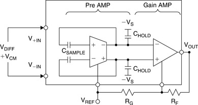
In Phase B, the differential signal is transferred to the hold capacitors refreshing the value stored on CHOLD. The output of the preamplifier is held at a common-mode voltage determined by the reference potential, VREF. In this manner, the AD8230 is able to condition the difference signal and set the output voltage level. The gain amplifier conditions the updated signal stored on the hold capacitors, CHOLD.
Resistance Temperature Detectors
The resistance temperature detector, or the RTD, is a sensor whose resistance changes with temperature. Typically built of a platinum (Pt) wire wrapped around a ceramic bobbin, the RTD exhibits behavior which is more accurate and more linear over wide temperature ranges than that of a thermocouple. Figure 3-42 illustrates the TC of a 100 Ω RTD and the Seebeck coefficient of a Type S thermocouple. Over the entire range (approximately −200°C to + 850°C), the RTD is a more linear device. Hence, linearizing an RTD is less complex.

Unlike a thermocouple, however, an RTD is a passive sensor and requires current excitation to produce an output voltage. The RTD’s low TC of 0.385%/°C requires similar high performance signal conditioning circuitry to that used by a thermocouple; however, the voltage drop across an RTD is much larger than a thermocouple output voltage. A system designer may opt for large value RTDs with higher output, but large-valued RTDs exhibit slow response times. Furthermore, although the cost of RTDs is higher than that of thermocouples, they use copper leads, and thermoelectric effects from terminating junctions do not affect their accuracy. And finally, because their resistance is a function of the absolute temperature, RTDs require no cold-junction compensation.
Caution must be exercised using current excitation because the current through the RTD causes heating. This self-heating changes the temperature of the RTD and appears as a measurement error. Hence, careful attention must be paid to the design of the signal conditioning circuitry so that self-heating is kept below 0.5°C. Manufacturers specify self-heating errors for various RTD values and sizes in still and in moving air. To reduce the error due to self-heating, the minimum current should be used for the required system resolution, and the largest RTD value chosen that results in acceptable response time.
Another effect that can produce measurement error is voltage drop in RTD lead wires. This is especially critical with low value two-wire RTDs because the TC and the absolute value of the RTD resistance are both small. If the RTD is located at a long distance from the signal conditioning circuitry, then the lead resistance can be ohms or tens of ohms, and a small amount of lead resistance can contribute a significant error to the temperature measurement. To illustrate this point, let us assume that a 100 Ω platinum RTD with 30-gauge copper leads is located about 100 feet from a controller’s display console. The resistance of 30-gauge copper wire is 0.105 Ω/feet, and the two leads of the RTD will contribute a total 21 Ω to the network which is shown in Figure 3-43. This additional resistance will produce a 55°C error in the measurement! The leads’ TC can contribute an additional, and possibly significant, error to the measurement. To eliminate the effect of the lead resistance, a four-wire technique is used.

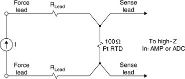
In Figure 3-44, a four-wire, or Kelvin, connection is made to the RTD. A constant current is applied though the FORCE leads of the RTD, and the voltage across the RTD itself is measured remotely via the SENSE leads. The measuring device can be a digital voltmeter (DVM) or an instrumentation amplifier, and high accuracy can be achieved provided that the measuring device exhibits high input impedance and/or low input bias current. Since the SENSE leads do not carry appreciable current, this technique is insensitive to lead wire length. Sources of errors are the stability of the constant current source and the input impedance and/or bias currents in the amplifier or DVM.
RTDs are generally configured in a four-resistor bridge circuit. The bridge output is amplified by an instrumentation amplifier for further processing. However, high resolution measurement ADCs such as the AD77XX series allow the RTD output to be digitized directly. In this manner, linearization can be performed digitally, thereby easing the analog circuit requirements.
Figure 3-45 shows a 100 Ω Pt RTD driven with a 400 μA excitation current source. The output is digitized by one of the AD77XX series ADCs. Note that the RTD excitation current source also generates the 2.5 V reference voltage for the ADC via the 6.25 kΩ resistor. Variations in the excitation current do not affect the circuit accuracy, since both the input voltage and the reference voltage vary ratiometrically with the excitation current. However, the 6.25 kΩ resistor must have a low TC to avoid errors in the measurement. The high resolution of the ADC and the input PGA (gain of 1–128) eliminates the need for additional conditioning circuits.

The ADT70 is a complete Pt RTD signal conditioner which provides an output voltage of 5 mV/°C when using a 1 kΩ RTD (see Figure 3-46). The Pt RTD and the 1 kΩ reference resistor are both excited with 1 mA matched current sources. This allows temperature measurements to be made over a range of approximately −50°C to +800°C.

The ADT70 contains the two matched current sources, a precision rail-to-rail output instrumentation amplifier, a 2.5 V reference, and an uncommitted rail-to-rail output op amp. The ADT71 is the same as the ADT70 except the internal voltage reference is omitted. A shutdown function is included for battery powered equipment that reduces the quiescent current from 3 mA to 10 μA. The gain or full-scale range for the Pt RTD and ADT701 system is set by a precision external resistor connected to the instrumentation amplifier. The uncommitted op amp may be used for scaling the internal voltage reference, providing a “Pt RTD open” signal or “over temperature” warning, providing a heater switching signal, or other external conditioning determined by the user. The ADT70 is specified for operation from −40°C to + 125°C and is available in 20-pin DIP and SOIC packages.
Thermistors
Similar in function to the RTD, thermistors are low cost temperature-sensitive resistors and are constructed of solid semiconductor materials which exhibit a positive or negative temperature coefficient (NTC). Although positive TC devices are available, the most commonly used thermistors are those with an NTC. Figure 3-47 shows the resistance–temperature characteristic of a commonly used NTC thermistor. The thermistor is highly nonlinear and, of the three temperature sensors discussed, is the most sensitive.

The thermistor’s high sensitivity (typically, −44,000 ppm/°C at 25°C, as shown in Figure 3-48), allows it to detect minute variations in temperature which could not be observed with an RTD or thermocouple. This high sensitivity is a distinct advantage over the RTD in that four-wire Kelvin connections to the thermistor are not needed to compensate for lead wire errors. To illustrate this point, suppose a 10 kΩ NTC thermistor, with a typical 25°C TC of −44,000 ppm/°C, were substituted for the 100 Ω Pt RTD in the example given earlier; then a total lead wire resistance of 21 Ω would generate less than 0.05°C error in the measurement. This is roughly a factor of 500 improvements in error over an RTD.

However, the thermistor’s high sensitivity to temperature does not come without a price. As was shown in Figure 3-48, the TC of thermistors does not decrease linearly with increasing temperature as it does with RTDs; therefore, linearization is required for all but the narrowest of temperature ranges. Thermistor applications are limited to a few hundred degrees at best because they are more susceptible to damage at high temperatures. Compared to thermocouples and RTDs, thermistors are fragile in construction and require careful mounting procedures to prevent crushing or bond separation. Although a thermistor’s response time is short due to its small size, its small thermal mass makes it very sensitive to self-heating errors.
Thermistors are very inexpensive, highly sensitive temperature sensors. However, we have shown that a thermistor’s TC varies from −44,000 ppm/°C at 25°C to −29,000 ppm/°C at 100°C. Not only is this nonlinearity the largest source of error in a temperature measurement, but also it limits useful applications to very narrow temperature ranges if linearization techniques are not used.
It is possible to use a thermistor over a wide temperature range only if the system designer can tolerate a lower sensitivity to achieve improved linearity. One approach to linearizing a thermistor is simply shunting it with a fixed resistor. Paralleling the thermistor with a fixed resistor increases the linearity significantly. As shown in Figure 3-49, the parallel combination exhibits a more linear variation with temperature compared to the thermistor itself. Also, the sensitivity of the combination still is high compared to a thermocouple or RTD. The primary disadvantage to this technique is that linearization can only be achieved within a narrow range.

The value of the fixed resistor can be calculated from the following equation:
where RT1 is the thermistor resistance at T1, the lowest temperature in the measurement range, RT3 is the thermistor resistance at T3, the highest temperature in the range, and RT2 is the thermistor resistance at T2, the midpoint, T2 = (T1 + T3)/2.
For a typical 10 kΩ NTC thermistor, RT1 = 32,650 Ω at 0°C, RT2 = 6,532 Ω at 35°C, and RT3 = 1,752 Ω at 70°C. This results in a value of 5.17 kΩ for R. The accuracy needed in the signal conditioning circuitry depends on the linearity of the network. For the example given above, the network shows a nonlinearity of −2.3°C/+2.0°C.
The output of the network can be applied to an ADC to perform further linearization as shown in Figure 3-50. Note that the output of the thermistor network has a slope of approximately −10 mV/°C, which implies a 12-bit ADC has more than sufficient resolution.

Digital Output Temperature Sensors
Temperature sensors which have digital outputs have a number of advantages over those with analog outputs, especially in remote applications. Opto-isolators can also be used to provide galvanic isolation between the remote sensor and the measurement system. A voltage-to-frequency converter driven by a voltage output temperature sensor accomplishes this function; however, more sophisticated ICs are now available which are more efficient and offer several performance advantages.
The TMP03/TMP04 digital output sensor family includes a voltage reference, VPTAT generator, sigma–delta ADC, and a clock source (see Figure 3-51). The sensor output is digitized by a first-order sigma–delta modulator, also known as the “charge balance” type ADC. This converter utilizes time-domain oversampling and a high accuracy comparator to deliver 12 bits of effective accuracy in an extremely compact circuit.
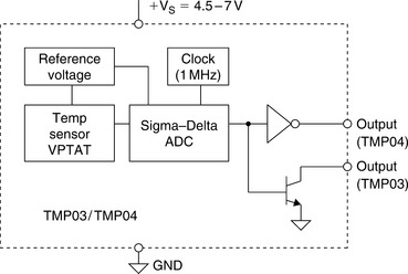
The output of the sigma–delta modulator is encoded using a proprietary technique which results in a serial digital output signal with a mark-space ratio format (see Figure 3-52) that is easily decoded by any microprocessor into either degrees centigrade or degrees Fahrenheit, and readily transmitted over a single wire. Most importantly, this encoding method avoids major error sources common to other modulation techniques, as it is clock-independent. The nominal output frequency is 35 Hz at +25°C, and the device operates with a fixed high level pulse width (T1) of 10 ms.

The TMP03/TMP04 output is a stream of digital pulses, and the temperature information is contained in the mark-space ratio as per the equations:
Popular microcontrollers, such as the 80C51 and 68HC11, have on-chip timers which can easily decode the mark-space ratio of the TMP03/TMP04. A typical interface to the 80C51 is shown in Figure 3-53. Two timers, labeled Timer 0 and Timer 1, are 16 bits in length. The 80C51’s system clock, divided by 12, provides the source for the timers. The system clock is normally derived from a crystal oscillator, so timing measurements are quite accurate. Since the sensor’s output is ratiometric, the actual clock frequency is not important. This feature is important because the microcontroller’s clock frequency is often defined by some external timing constraint, such as the serial baud rate.
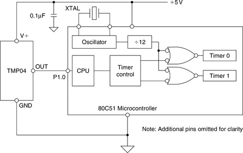
Software for the sensor interface is straightforward. The microcontroller simply monitors I/O port P1.0, and starts Timer 0 on the rising edge of the sensor output. The microcontroller continues to monitor P1.0, stopping Timer 0 and starting Timer 1 when the sensor output goes low. When the output returns high, the sensor’s T1 and T2 times are contained in registers Timer 0 and Timer 1, respectively. Further software routines can then apply the conversion factor shown in the equations above and calculate the temperature.
Thermostatic Switches and Setpoint Controllers
Temperature sensors used in conjunction with comparators can act as thermostatic switches. ICs such as the AD22105 accomplish this function at low cost and allow a single external resistor to program the setpoint to 2°C accuracy over a range of −40°C to + 150°C (see Figure 3-54). The device asserts an open collector output when the ambient temperature exceeds the user-programmed setpoint temperature. The ADT05 has approximately 4°C of hysteresis which prevents rapid thermal on/off cycling. The ADT05 is designed to operate on a single-supply voltage from + 2.7 to + 7.0 V facilitating operation in battery powered applications as well as industrial control systems. Because of low power dissipation (200 μW@ 3.3 V), self-heating errors are minimized, and battery life is maximized. An optional internal 200 kΩ pull-up resistor is included to facilitate driving light loads such as CMOS inputs.

The setpoint resistor is determined by the equation:
The setpoint resistor should be connected directly between the RSET pin (Pin 4) and the GND pin (Pin 5). If a ground plane is used, the resistor may be connected directly to this plane at the closest available point.
The setpoint resistor can be of nearly any resistor type, but its initial tolerance and thermal drift will affect the accuracy of the programmed switching temperature. For most applications, a 1% metal-film resistor will provide the best tradeoff between cost and accuracy. Once RSET has been calculated, it may be found that the calculated value does not agree with readily available standard resistors of the chosen tolerance. In order to achieve a value as close as possible to the calculated value, a compound resistor can be constructed by connecting two resistors in series or parallel.
The TMP01 is a dual setpoint temperature controller which also generates a PTAT output voltage (see Figure 3-55). It also generates a control signal from one of two outputs when the device is either above or below a specific temperature range. Both the high/low temperature trip points and hysteresis band are determined by user-selected external resistors.

The TMP01 consists of a bandgap voltage reference combined with a pair of matched comparators. The reference provides both a constant 2.5 V output and a PTAT output voltage which has a precise TC of 5 mV/K and is 1.49 V (nominal) at +25°C. The comparators compare VPTAT with the externally set temperature trip points and generate an open collector output signal when one of their respective thresholds has been exceeded.
Hysteresis is also programmed by the external resistor chain and is determined by the total current drawn out of the 2.5 V reference. This current is mirrored and used to generate a hysteresis offset voltage of the appropriate polarity after a comparator has been tripped. The comparators are connected in parallel, which guarantees that there is no hysteresis overlap and eliminates erratic transitions between adjacent trip zones.
Microprocessor Temperature Monitoring
Today’s computers require that hardware as well as software operate properly, in spite of the many things that can cause a system crash or lockup. The purpose of hardware monitoring is to monitor the critical items in a computing system and take corrective action so that problems do not occur.
Microprocessor supply voltage and temperature are two critical parameters. If the supply voltage drops below a specified minimum level, further operations should be halted until the voltage returns to acceptable levels. In some cases, it is desirable to reset the microprocessor under “brownout” conditions. It is also common practice to reset the microprocessor on power-up or power-down. Switching to a battery backup may be required if the supply voltage is low.
Under low voltage conditions it is mandatory to inhibit the microprocessor from writing to external CMOS memory by inhibiting the Chip Enable signal to the external memory.
Many microprocessors can be programmed to periodically output a “watchdog” signal. Monitoring this signal gives an indication that the processor and its software are functioning properly and that the processor is not stuck in an endless loop.
The need for hardware monitoring has resulted in a number of ICs, traditionally called “microprocessor supervisory products,” which perform some or all of the above functions. These devices range from simple manual reset generators (with debouncing) to complete microcontroller-based monitoring sub-systems with on-chip temperature sensors and ADCs. ADI’ ADM family of products is specifically to perform the various microprocessor supervisory functions required in different systems.
CPU temperature is critically important in the Pentium microprocessors. For this reason, all new Pentium devices have an on-chip substrate PNP transistor which is designed to monitor the actual chip temperature. The collector of the substrate PNP is connected to the substrate, and the base and emitter are brought out on two separate pins of the Pentium II.
The ADM1021 Microprocessor Temperature Monitor is specifically designed to process these outputs and convert the voltage into a digital word representing the chip temperature. The simplified analog signal processing portion of the ADM1021 is shown in Figure 3-56.

The technique used to measure the temperature is identical to the “ΔVBE” principle previously discussed. Two different currents (I and N·I) are applied to the sensing transistor, and the voltage measured for each. In the ADM1021, the nominal currents are I = 6 μA, (N = 17), N·I = 102 μA.
The change in the base-emitter voltage, ΔVBE, is a PTAT voltage and given by the equation:
Figure 3-56 shows the external sensor as a substrate transistor, provided for temperature monitoring in the microprocessor, but it could equally well be a discrete transistor. If a discrete transistor is used, the collector should be connected to the base and not grounded. To prevent ground noise interfering with the measurement, the more negative terminal of the sensor is not referenced to ground, but is biased above ground by an internal diode. If the sensor is operating in a noisy environment, C may be optionally added as a noise filter. Its value is typically 2200 pF, but should be no more than 3000 Pf.
To measure ΔVBE, the sensing transistor is switched between operating currents of I and N·I. The resulting waveform is passed through a 65 kHz lowpass filter to remove noise, then to a chopper-stabilized amplifier which performs the function of amplification and synchronous rectification. The resulting DC voltage is proportional to ΔVBE and is digitized by an 8-bit ADC. To further reduce the effects of noise, digital filtering is performed by averaging the results of 16 measurement cycles.
In addition, the ADM1021 contains an on-chip temperature sensor, and its signal conditioning and measurement are performed in the same manner.
One least significant bit (LSB) of the ADC corresponds to 1°C, so the ADC can theoretically measure from −128°C to + 127°C, although the practical lowest value is limited to −65°C due to device maximum ratings. The results of the local and remote temperature measurements are stored in the local and remote temperature value registers, and are compared with limits programmed into the local and remote high and low limit registers as shown in Figure 3-57. An ALERT output signals when the on-chip or remote temperature is out of range. This output can be used as an interrupt, or as a system management bus (SMBus) alert.

The limit registers can be programmed, and the device controlled and configured, via the serial SMBus. The contents of any register can also be read back by the SMBus. Control and configuration functions consist of: switching the device between normal operation and standby mode, masking or enabling the ALERT output, and selecting the conversion rate which can be set from 0.0625 to 8 Hz.
References: Temperature Sensors
1 Pallas-Areny R., Webster J.G. Sensors and Signal Conditioning. New York: John Wiley, 1991.
2 Sheingold D., ed. Transducer Interfacing Handbook. Inc.: Analog Devices, 1980. Norwood, Ma.
3 Kester W., ed. 1992 Amplifier Applications Guide, Section 2, 3. Inc.: Analog Devices, 1992. Norwood, Ma.
4 Kester W., ed. System Applications Guide, Section 1, 6. Inc.: Analog Devices, 1993. Norwood, Ma.
5 Sheingold D. Nonlinear Circuits Handbook. Inc.: Analog Devices, 1980. Norwood, Ma.
6 J. Wong, “Temperature Measurements Gain from Advances in High-precision Op Amps,” Electronic Design, May 15, 1986.
7 OMEGA Temperature Measurement Handbook, Omega Instruments, Inc.
8 Handbook of Chemistry and Physics, CRC
9 P. Brokaw, “A Simple Three-Terminal IC Bandgap Voltage Reference,” IEEE Journal of Solid State Circuits, No. SC-9, 1974.
SECTION 3-3 Charge Coupled Devices
Charge coupled devices (CCDs) contain a large number of small photocells called photosites or pixels which are arranged either in a single row (linear arrays) or in a matrix (area arrays). CCD area arrays are commonly used in video applications, while linear arrays are used in facsimile machines, graphics scanners, and pattern recognition equipment.
The linear CCD array consists of a row of image sensor elements (photosites, or pixels) which are illuminated by light from the object or document. During one exposure period each photosite acquires an amount of charge which is proportional to its illumination. These photosite charge packets are subsequently switched simultaneously via transfer gates to an analog shift register. The charge packets on this shift register are clocked serially to a charge detector (storage capacitor) and buffer amplifier (source follower), which convert them into a string of photo-dependent output voltage levels (see Figure 3-58). While the charge packets from one exposure are being clocked out to the charge detector, another exposure is underway. The analog shift register typically operates at frequencies between 1 and 10 MHz.

The charge detector readout cycle begins with a reset pulse which causes a FET switch to set the output storage capacitor to a known voltage. The switching FET’s capacitive feedthrough causes a reset glitch at the output as shown in Figure 3-59. The switch is then opened, isolating the capacitor, and the charge from the last pixel is dumped onto the capacitor causing a voltage change. The difference between the reset voltage and the final voltage (video level), shown in Figure 3.59, represents the amount of charge in the pixel. CCD charges may be as low as 10 electrons, and a typical CCD output sensitivity is 0.6 μV/electron. Most CCDs have a saturation output voltage of about 1 V (see Reference 16).
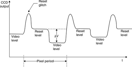
Since CCDs are generally fabricated on MOS processes, they have limited capability to perform on-chip signal conditioning. Therefore the CCD output is generally processed by external conditioning circuits.
CCD output voltages are small and quite often buried in noise. The largest source of noise is the thermal noise in the resistance of the FET reset switch. This noise may have a typical value of 100–300 electrons root mean square (RMS) (approximately 60–180 mVRMS). This noise occurs as a sample-to-sample variation in the CCD output level and is common to both the reset level and the video level for a given pixel period. A technique called correlated double sampling (CDS) is often used to reduce the effect of this noise. Figure 3.60 shows two circuit implementations of the CDS scheme. In the top circuit, the CCD output drives both sample-and-hold amplifiers (SHAs). At the end of the reset interval, SHA1 holds the reset voltage level. At the end of the video interval, SHA2 holds the video level. The SHA outputs are applied to a difference amplifier which subtracts one from the other. In this scheme, there is only a short interval during which both SHA outputs are stable, and their difference represents ΔV, so the difference amplifier must settle quickly.

Another arrangement is shown in the bottom half of Figure 3-60, which uses three SHAs and allows for either faster operation or more time for the difference amplifier to settle. In this circuit, SHA1 holds the reset level so that it occurs simultaneously with the video level at the input to SHA2 and SHA3. When the video clock is applied simultaneously to SHA2 and SHA3, the input to SHA2 is the reset level, and the input to SHA3 the video level. This arrangement allows the entire pixel period (less the acquisition time of SHA2 and SHA3) for the difference amplifier to settle.
References: Charge Coupled Devices
1 Kester W., ed. 1992 Amplifier Applications Guide, Section 2, 3. Inc.: Analog Devices, 1992. Norwood, Ma.
2 Kester W., ed. System Applications Guide, Section 1, 6. Inc.: Analog Devices, 1993. Norwood, Ma.
3 Optoelectronics Data Book. St. Louis, MO: EG&G Vactec; 1990.
4 Silicon Detector Corporation, Camarillo, CA, Part Number SD-020-12-001 Data Sheet.
5 Photodiode 1991 Catalog, Hamamatsu Photonics, Bridgewater, NJ
6 Morrison R. Grounding and Shielding Techniques in Instrumentation, 3rd Edition, Inc.: John Wiley, 1986.
7 Ott H.W. Noise Reduction Techniques in Electronic Systems, 2nd Edition, Inc.: John Wiley, 1988.
8 An Introduction to the Imaging CCD Array. Beaverton, OR: Tektronix, Inc.; 1987. Technical Note 82W-4022.