CHAPTER 2 Other Linear Circuits
![]() Section 2-1: Buffer Amplifiers
Section 2-1: Buffer Amplifiers
![]() Section 2-3: Instrumentation Amplifiers
Section 2-3: Instrumentation Amplifiers
![]() Section 2-4: Differential Amplifiers
Section 2-4: Differential Amplifiers
![]() Section 2-5: Isolation Amplifiers
Section 2-5: Isolation Amplifiers
![]() Section 2-6: Digital Isolation Techniques
Section 2-6: Digital Isolation Techniques
![]() Section 2-7: Active Feedback Amplifiers
Section 2-7: Active Feedback Amplifiers
![]() Section 2-8: Logarithmic Amplifiers
Section 2-8: Logarithmic Amplifiers
![]() Section 2-9: High Speed Clamping Amplifiers
Section 2-9: High Speed Clamping Amplifiers
![]() Section 2-11: Analog Multipliers
Section 2-11: Analog Multipliers
![]() Section 2-12: RMS to DC Converters
Section 2-12: RMS to DC Converters
![]() Section 2-13: Programmable Gain Amplifiers
Section 2-13: Programmable Gain Amplifiers
SECTION 2-1 Buffer Amplifiers
In the early days of high speed circuits, simple emitter followers were often used as high speed buffers. The term buffer was generally accepted to mean a unity-gain, open-loop amplifier. With the availability of matching PNP transistors, a simple emitter follower can be improved, as shown in Figure 2-1(A). This complementary circuit offers first-order cancellation of DC offset voltage, and can achieve bandwidths greater than 100 MHz. Typical offset voltages without trimming are usually less than 50 mV, even with unmatched discrete transistors.

If high input impedance is required, a dual FET can be used as an input stage ahead of a complementary emitter follower, as shown in Figure 2-1(B). This form of the buffer circuit was implemented by both National Semiconductor Corporation as the LH0033, and by Analog Devices as the ADLH0033.
Circuits such as these achieved bandwidths of about 100 MHz at fairly respectable levels of harmonic distortion, typically better than −60 dBc. However, they suffered from DC and AC nonlinearities when driving loads less than 500 Ω.
One of the first totally monolithic implementations of these functions was the Precision Monolithics, Inc. BUF03 shown in Figure 2-2 (see Reference 1). PMI is now a division of Analog Devices. This open-loop IC buffer achieved a bandwidth of about 50 MHz for a 2 V peak-to-peak signal.

The BUF03 circuit is interesting because it demonstrates techniques that eliminated the requirement for the slow, bandwidth-limited vertical PNP transistors associated with most IC processes available at the time of the design (approximately 1979).
One of the problems with all the open-loop buffers discussed thus far is that although high bandwidths can be achieved, the devices discussed do not take advantage of negative feedback. Distortion and DC performance suffer considerably when open-loop buffers are loaded with typical video impedance levels of 50, 75, or 100 Ω. The solution is to use a properly compensated wide bandwidth op amp in a unity-gain follower configuration. In the early days of monolithic op amps, process limitations prevented this, so the open-loop approach provided a popular interim solution (Figure 2-3).
Practically all unity-gain stable voltage or current feedback op amps can be used in a simple follower configuration. Usually, however, the general-purpose op amps are compensated to operate over a wide range of gains and feedback conditions. Therefore, bandwidth suffers somewhat at low gains, especially in the unity-gain non-inverting mode, and additional external compensation is usually required, as shown in Figure 2-4.
A practical solution is to compensate the op amp for the desired closed-loop gain, while including the gain-setting resistors on-chip. Note that this form of op amp, internally configured as a buffer, may typically have no feedback pin. Also, putting the resistors and compensation on-chip serves to reduce parasitics.
There are a number of op amps optimized in this manner. Roy Gosser’s AD9620 (see Reference 2) was probably the earliest monolithic implementation. The AD9620 was a 1990 product release, and achieved a bandwidth of 600 MHz using ±5 V supplies. It was optimized for unity gain, and used the voltage feedback architecture. A newer design based on similar techniques is the AD9630, which achieves a 750 MHz bandwidth.
The BUF04 unity-gain buffer (see Reference 3) was released in 1994 and achieves a bandwidth of 120 MHz. This device was optimized for large signals and operates on supplies from ±5 V to ± 15 V. Because of the wide supply range, the BUF04 is useful not only as a standalone unit-gain buffer, but also within a feedback loop with a standard op amp, to boost output.
Although the common definition of a buffer is unity-gain device, sometimes the term is used for a circuit with a gain of two. Closed-loop buffers with a gain of two find wide applications as transmission line drivers, as shown in Figure 2-5. The internally configured fixed gain of the amplifier compensates for the loss incurred by the source and load termination. Impedances of 50, 75, and 100 Ω are popular cable impedances. The AD8074/AD8075 500 MHz triple buffers are optimized for gains of 1 and 2, respectively. The dual AD8079A/AD8079B 260 MHz buffer is optimized for gains of 2 and 2.2, respectively.

In implementing a high speed unity-gain buffer with a voltage feedback op amp, there will typically be no resistor required in the feedback loop, which considerably simplifies the circuit. Note that this is not a 100% hard-and-fast rule however, so always check the device data sheet to be sure. A unity-gain buffer with a current feedback op amp will always require a feedback resistor, typically in the range of 500–1,000 Ω. So, be sure to use a value appropriate to not only the basic part, but also the specific power supplies in use.
SECTION 2-2 Gain Blocks
While the op amp allows gain to be set with external resistors, there are a group of circuits that are designed to operate at a fixed gain. These parts are typically RF components. They are also typically designed to be operated in a 50 Ω environment, with the inputs and outputs matched internally. Often the gain blocks are available in several gain settings.
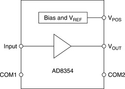
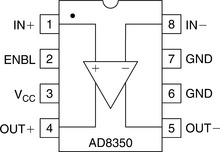
For example, the AD8354 RF gain block is a fixed-gain amplifier with single-ended input and output ports whose impedances are nominally equal to 50 Ω over the frequency range 100 MHz to 2.7 GHz. Consequently, it can be directly inserted into a 50 Ω system with no impedance matching circuitry required. The input and output impedances are sufficiently stable versus variations in temperature and supply voltage that no impedance matching compensation is required (Figure 2-6).
Differential input and output gain blocks are also available. An example of a differential input, single-ended output device is the AD8129 (see Figure 2-7).

Fully differential input and output devices are also available, such as the AD8350 (see Figure 2-8).
SECTION 2-3 Instrumentation Amplifiers
The instrumentation amp is primarily used to amplify small differential voltages in the presence of (typically) larger common-mode (CM) voltages.
In Amp Definitions
An in amp is a precision closed-loop gain block. It has a pair of differential input terminals, and a single-ended output that works with respect to a reference or common terminal, as shown in Figure 2-9. The input impedances are balanced and high in value, typically ≥ 109 Ω. Again, unlike an op amp, an in amp uses an internal feedback resistor network, plus one (usually) gain set resistance, RG. Also unlike an op amp is the fact that the internal resistance network and RG are isolated from the signal input terminals. In amp gain can also be preset via an internal RG by pin selection (again isolated from the signal inputs). Typical in amp gains range from 1 to 1,000.

The in amp develops an output voltage which is referenced to a pin usually designated REFERENCE or VREF. In many applications, this pin is connected to circuit ground, but it can be connected to other voltages, as long as they lie within the rated compliance range of the in amp. This feature is especially useful in single-supply applications, where the output voltage is usually referenced to mid-supply (i.e., +2.5 V in the case of a + 5 V supply).
In order to be effective, an in amp needs to be able to amplify microvolt-level signals, while simultaneously rejecting volts of CM signal at its inputs. This requires that in amps have very high common-mode rejection (CMR). Typical values of in amp CMR are from 70 to over 100 dB (at DC), with CMR usually improving at higher gains.
It is important to note that a CMR specification for DC inputs alone is not sufficient in most practical applications. In industrial applications, the most common cause of external interference is 50/60 Hz AC power-related noise (including harmonics). In differential measurements, this type of interference tends to be induced equally onto both in amp inputs, so the interference appears as a CM input signal. Therefore, specifying CMR over frequency is just as important as specifying its DC value. Note that imbalance in the two source impedances will degrade the CMR of some in amps. Analog Devices fully specifies in amp CMR at 50/60 Hz, with a source impedance imbalance of 1 kΩ.
Op Amp/In Amp Functionality Differences
An op amp is a general-purpose gain block—user-configurable in myriad ways using external feedback components of R, C, and (sometimes) L. The final configuration and circuit function using an op amp is truly whatever you make of it.
In contrast to this, an instrumentation amp (in amp) is a more constrained device in terms of functioning, and also the allowable range(s) of operating gain. People also often confuse in amps as to their function, calling them “op amps.” But the converse is seldom (if ever) true. It should be understood that an in amp is not just a special type op amp; the function of the two devices is actually fundamentally different.
Perhaps a good way to differentiate the two devices is to remember that an op amp can be programmed to do almost anything, by virtue of its feedback flexibility. In contrast to this, an in amp cannot be programmed to do just anything. It can only be programmed for gain, and then over a specific range. An op amp is configured via a number of external components, while an in amp is configured by either one resistor, or by pin-selectable taps for its working gain.
Subtractor or Difference Amplifiers
A simple subtractor or difference amplifier can be constructed with four resistors and an op amp as shown in Figure 2-10. It should be noted that this is not a true in amp, but it is often used in applications where a simple differential to single-ended conversion is required. Because of its popularity, this circuit will be examined in more detail in order to understand its fundamental limitations before discussing true in amp architectures.
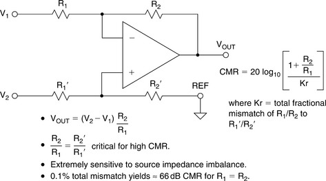
There are several fundamental problems with this simple circuit. First, the input impedance seen by V1 and V2 is not balanced. The input impedance seen by V1 is R1, but the input impedance seen by V2 is R1′+R2′. The configuration can also be quite problematic in terms of CMR, since even a small source impedance imbalance will degrade the workable CMR. This problem can be solved with well-matched open-loop buffers in series with each input (e.g., using a precision dual op amp). But this adds complexity to a simple circuit, and may introduce offset drift and nonlinearity.
The second problem with this circuit is that the CMR is primarily determined by the resistor ratio matching, not the op amp. The resistor ratios R1/R2 and R1′/R2′ must match extremely well to reject CM noise—at least as well as a typical op amp CMR of 100 dB. Note also that the absolute resistor values are relatively unimportant.
Picking four 1% resistors from a single batch may yield a net ratio matching of 0.1%, which will achieve a CMR of 66 dB (assuming R1 = R2). But if one resistor differs from the rest by 1%, the CMR will drop to only 46 dB. Clearly, very limited performance is possible using ordinary discrete resistors in this circuit (without resorting to hand matching). This is because the best standard off-the-shelf RNC/RNR style resistor tolerances are on the order of 0.1% (see Reference 1).
In general, the worst-case CMR for a circuit of this type is given by the following equation (see References 2 and 3):
where Kr is the individual resistor tolerance in fractional form, for the case where four discrete resistors are used. This equation shows that the worst-case CMR for a tolerance build-up for four unselected same-nominal-value 1% resistors is no better than 34 dB.
A single resistor network with a net matching tolerance of Kr would probably be used for this circuit, in which case the expression would be as noted in the Figure, or:
A net matching tolerance of 0.1% in the resistor ratios therefore yields a worst-case DC CMR of 66 dB using Eq. (2-2), and assuming R1 = R2. Note that either case assumes a significantly higher amplifier CMR (i.e., >100 dB). Clearly for high CMR, such circuits need four single-substrate resistors, with very high absolute and TC matching. Such networks using thick-/thin-film technology are available from companies such as Caddock and Vishay, in ratio matches of 0.01% or better.
In implementing the simple difference amplifier, rather than incurring the higher costs and PCB real estate limitations of a precision op amp plus a separate resistor network, it is usually better to seek out a completely monolithic solution.
An interesting variation on the simple difference amplifier is found in the AD629 difference amplifier, optimized for high CM input voltages. A typical current-sensing application is shown in Figure 2-11. The AD629 is a differential to single-ended amplifier with a gain of unity. It can handle a CM voltage of ±270 V with supply voltages of ± 15 V, with a small signal bandwidth of 500 kHz.

The high CM voltage range is obtained by attenuating the non-inverting input (pin 3) by a factor of 20 times, using the R1−R2 divider network. On the inverting input, resistor R5 is chosen such that R5?R3 equals resistor R2. The noise gain of the circuit is equal to 20 [1 + R4/(R3‖R5)], thereby providing unity gain for differential input voltages. Laser wafer trimming of the R1−R5 thin-film resistors yields a minimum CMR of 86 dB @ 500 Hz for the AD629B. Within an application, it is good practice to maintain balanced source impedances on both inputs, so dummy resistor RCOMP is chosen to equal to the value of the shunt-sensing resistor RSHUNT.
The Three Op Amp Instrumentation Amplifier Topology
For the highest precision and performance, the three op amp instrumentation amplifier topology is optimum for bridge and other offset transducer applications where high accuracy and low nonlinearity are required (Figure 2-12).

Resistor RG sets the overall gain of this amplifier. It may be internal, external, or (software or pin-strap) programmable, depending on the particular in amp. In this configuration, CMR depends on the ratio matching of R3/R2 to R3′/R2′. Furthermore, CM signals are only amplified by a factor of 1 regardless of gain (no CM voltage will appear across RG, hence, no CM current will flow in it because the input terminals of an op amp will have no significant potential difference between them).
As a result of the high ratio of differential to CM gain in A1–A2, CMR of this in amp theoretically increases in proportion to gain. Large CM signals (within the A1–A2 op amp headroom limits) may be handled at all gains. Finally, because of the symmetry of this configuration, CM errors in the input amplifiers, if they track, tend to be canceled out by the subtractor output stage. These features explain the popularity of this three op amp in amp configuration—it is capable of delivering the highest performance.
The classic three op amp configuration has been used in a number of monolithic IC in amps (see References 8 and 9). Besides offering excellent matching between the three internal op amps, thin-film laser-trimmed resistors provide excellent ratio matching and gain accuracy at much lower cost than using discrete precision op amps and resistor networks. The AD620 (see Reference 10) is an excellent example of monolithic IC in amp technology. A simplified device schematic is shown in Figure 2-13.

The AD620 is a highly popular in amp and is specified for power supply voltages from ±2.3 V to ± 18 V. Input voltage noise is only 9 nV/Hz @ 1 kHz. Maximum input bias current is only 1 nA, due to the use of superbeta transistors for Q1–Q2.
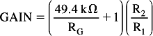
Overvoltage protection is provided, in part, by the internal 400 Ω thin-film current-limit resistors in conjunction with the diodes connected from the emitter-to-base of Q1 and Q2. The gain G is set with a single external RG resistor, as noted by Eq. (2-3):
 (2-3)
(2-3)As can be noted from this expression and Figure 2-13, the AD620 internal resistors are trimmed so that standard 1% or 0.1% resistors can be used to set gain to popular values. Single-supply operation of the three op amp in amp requires an understanding of the internal node voltages. Figure 2-14 shows a generalized diagram of the in amp operating on a single + 5 V supply. The maximum and minimum allowable output voltages of the individual op amps are designated VOH (maximum high output) and VOL (minimum low output), respectively.

Note that the gain from the CM voltage to the outputs of A1 and A2 is unity. It can be stated that the sum of the CM voltage and the signal voltage at these outputs must fall within the amplifier output voltage range. Obviously this configuration cannot handle input CM voltages of either 0 V or +5 V, because of saturation of A1 and A2. The output reference is positioned halfway between VOH and VOL to allow for bipolar differential input signals.
While there are a number of good single supply in amps, such as the AD627, the highest performance devices are still among those specified for traditional dual-supply operation, i.e., the just-discussed AD620. For certain applications, even devices such as the AD620, which has been designed for dual-supply operation, can be used with full precision on a single-supply power system.
Precision Single-Supply Composite In Amp
One way to achieve both high precision and single-supply operation takes advantage of the fact that many popular sensors (e.g., strain gauges) provide an output signal which is inherently centered around an approximate midpoint of the supply voltage (and/or the reference voltage). Taking advantage of this basic point allows the inputs of a signal conditioning in amp to be biased at “mid-supply.” As a consequence of this step, the inputs need not operate near ground or the positive supply voltage, and the in amp can still be used with all its precision.
Under these conditions, an AD620 dual-supply in amp referenced to the supply midpoint followed by a rail-to-rail op amp output-gain stage provides very high DC precision. Figure 2-15 illustrates one such high performance in amp, which operates on a single + 5 V supply.

This circuit uses the AD620 as a low cost precision in amp for the input stage, along with an AD822 JFET input dual rail-to-rail output op amp for the output stage, comprising A1 and A2. The output stage operates at a fixed gain of 3, with overall gain set by RG.
In this circuit, R3 and R4 form a voltage divider which splits the supply voltage nominally in half to +2.5 V, with fine adjustment provided by a trimming potentiometer, P1. This voltage is applied to the input of A1, an AD822 voltage follower, which buffers it and provides a low impedance source needed to drive the AD620’s reference pin as well as providing the output reference voltage VREF. Note that this feature allows a bipolar VOUT to be measured with respect to this +2.5 V reference (not to GND). This is despite the fact that the entire circuit operates from a single (unipolar) supply.
The other half of the AD822 is connected as a gain of 3 inverter, so that it can output ±2.5 V, “rail-to-rail,” with only ±0.83 V required of the AD620. This output voltage level of the AD620 is well within the AD620’s capability, thus ensuring high linearity for the front end.
The general-gain expression for this composite in amp is the product of the gain of the AD620 stage, and the gain of inverting amplifier:
 (2-4)
(2-4)For this example, an overall gain of 10 is realized with RG = 21.5 kΩ (closest standard value). The table shown in Figure 2-16 summarizes various RG gain values, and the resulting performance for gains ranging from 10 to 1,000.
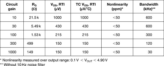
In this application, the allowable input voltage on either input to the AD620 must lie between + 2 V and + 3.5 V in order to maintain linearity. For example, at an overall circuit gain of 10, the CM input voltage range spans from 2.25 V to 3.25 V, allowing room for the ±0.25 V full-scale differential input voltage required to drive the output ±2.5 V about VREF.
The inverting configuration was chosen for the output buffer to facilitate system output offset voltage adjustment by summing currents into the A2 stage buffer’s feedback summing node. These offset currents can be provided by an external DAC, or from a resistor connected to a reference voltage.
To reduce the effects of unwanted noise pickup, a filter capacitor is recommended across A2’s feedback resistance to limit the circuit bandwidth to the frequencies of interest. This capacitor forms a first-order lowpass filter with R2. The corner frequency is 10 Hz as shown, but this may be easily modified. The capacitor should be a high quality film type, such as polypropylene.
The Two Op Amp Instrumentation Amplifier Topology
The circuit shown in Figure 2-17 is referred to as the two op amp in amp. It is particularly applicable in single-supply systems. Dual IC op amps are used in most cases for good matching, such as the OP297 or the OP284. Most often a rail-to-rail op amp is indicated. The resistors are often a thin-film laser-trimmed array, possibly on the same chip. The in amp gain can be easily set with an external resistor, RG. Without RG, the gain is simply 1 + R2/R1. In a practical application, the R2/R1 ratio is chosen for the desired minimum in amp gain.

The input impedance of the two op amp in amp is inherently high, permitting the impedance of the signal sources to be high and unbalanced. The DC CM rejection is limited by the matching of R1/R2 to R1′/R2′. If there is a mismatch in any of the four resistors, the DC CM rejection is limited to:
Notice that the net CMR of the circuit increases proportionally with the working gain of the in amp, an effective aid to high performance at higher gains.
IC in amps are particularly well suited to meeting the combined needs of ratio matching and temperature tracking of the gain-setting resistors. While thin-film resistors fabricated on silicon have an initial tolerance of up to ± 20%, laser trimming during production allows the ratio error (not absolute value) between the resistors to be reduced to 0.01% (100 ppm). Furthermore, the tracking between the temperature coefficients of the thin-film resistors is inherently low and is typically less than 3 ppm/°C (0.0003%/°C).
When dual supplies are used, VREF is normally connected directly to ground. In single-supply applications, VREF is usually connected to a low impedance voltage source equal to one-half the supply voltage. The gain from VREF to node “A” is R1/R2, and the gain from node “A” to the output is R2′/R1′. This makes the gain from VREF to the output equal to unity, assuming perfect ratio matching. Note that it is critical that the source impedance seen by VREF be low; otherwise, CMR will be degraded.
One major disadvantage of the two op amp in amp design is that CM voltage input range must be traded off against gain. The amplifier A1 must amplify the signal at V1 by 1 + R1/R2. If R1 ![]() R2 (a low gain example in Figure 2-18), A1 will saturate if the V1 CM signal is too high, leaving no A1 headroom to amplify the wanted differential signal. For high gains (R1
R2 (a low gain example in Figure 2-18), A1 will saturate if the V1 CM signal is too high, leaving no A1 headroom to amplify the wanted differential signal. For high gains (R1 ![]() R2), there is correspondingly more headroom at node “A,” allowing larger CM input voltages.
R2), there is correspondingly more headroom at node “A,” allowing larger CM input voltages.

The AC CM rejection of this configuration is generally poor because the signal path from V1 to VOUT has the additional phase shift of A1. In addition, the two amplifiers are operating at different closed-loop gains (and thus at different bandwidths). The use of a small trim capacitor “C” as shown in Figure 2-17 can improve the AC CMR somewhat.
A low gain (G = 2) single-supply two op amp in amp configuration results when RG is not used, and is shown in Figure 2-18. The input CM and differential signals must be limited to values which prevent saturation of either A1 or A2. In the example, the op amps remain linear to within 0.1 V of the supply rails, and their upper and lower output limits are designated VOH and VOL, respectively. These saturation voltage limits would be typical for a single-supply, rail–rail output op amp (such as the AD822).
Using the Figure 2-18 equations, the voltage at V1 must fall between 1.3 V and 2.4 V to prevent A1 from saturating. Notice that VREF is connected to the average of VOH and VOL (2.5 V). This allows for bipolar differential input signals with VOUT referenced to +2.5 V.
A high gain (G = 100) single-supply two op amp in amp configuration is shown in Figure 2-19. Using the same equations, note that voltage at V1 can now swing between 0.124 V and 4.876 V. VREF is again 2.5 V, to allow for bipolar input and output signals.

All of these discussions show that the conventional two op amp in amp architecture is fundamentally limited, when operating from a single power supply. These limitations can be viewed in one sense as a restraint on the allowable input CM range for a given gain. Or, alternately, it can be viewed as limitation on the allowable gain range, for a given CM input voltage.
In summary, regardless of gain, the basic structure of the common two op amp in amp does not allow for CM input voltages of zero when operated on a single supply. The only route to removing these restrictions for single-supply operation is to modify the in amp architecture.
In Amp DC Error Sources
The DC and noise specifications for in amps differ slightly from conventional op amps, so some discussion is required in order to fully understand the error sources.
The gain of an in amp is usually set by a single resistor. If the resistor is external to the in amp, its value is either calculated from a formula or chosen from a table on the data sheet, depending on the desired gain.
Absolute value laser wafer trimming allows the user to program gain accurately with this single resistor. The absolute accuracy and temperature coefficient of this resistor directly affects the in amp gain accuracy and drift. Since the external resistor will never exactly match the internal thin-film resistor tempcos, a low TC (<25 ppm/°C) metal film resistor should be chosen, preferably with a 0.1% or better accuracy.
Often specified as having a gain range of 1 to 1,000, or 1 to 10,000, many in amps will work at higher gains, but the manufacturer will not guarantee a specific level of performance at these high gains. In practice, as the gain-setting resistor becomes smaller, any errors due to the resistance of the metal runs and bond wires become significant. These errors, along with an increase in noise and drift, may make higher single-stage gains impractical. In addition, input offset voltages can become quite sizable when reflected to output at high gains. For instance, a 0.5 mV input offset voltage becomes 5 V at the output for a gain of 10,000. For high gains, the best practice is to use an in amp as a preamplifier; then use a post amplifier for further amplification.
In a pin-programmable-gain in amp such as the AD621, the gain-set resistors are internal, well matched, and the device gain accuracy and gain drift specifications include their effects. The AD621 is otherwise generally similar to the externally gain-programmed AD620.
The gain error specification is the maximum deviation from the gain equation. Monolithic in amps such as the AD624C have very low factory trimmed gain errors, with its maximum error of 0.02% at G = 1 and 0.25% at G = 500 being typical for this high quality in amp. Notice that the gain error increases with increasing gain. Although externally connected gain networks allow the user to set the gain exactly, the temperature coefficients of the external resistors and the temperature differences between individual resistors within the network all contribute to the overall gain error. If the data is eventually digitized and presented to a digital processor, it may be possible to correct for gain errors by measuring a known reference voltage and then multiplying by a constant.
Nonlinearity is defined as the maximum deviation from a straight line on the plot of output versus input. The straight line is drawn between the end-points of the actual transfer function. Gain nonlinearity in a high quality in amp is usually 0.01% (100 ppm) or less, and is relatively insensitive to gain over the recommended gain range.
The total input offset voltage of an in amp consists of two components (see Figure 2-20): input offset voltage, VOSI, is the input offset component that is reflected to the output of the in amp by the gain G; output offset voltage, VOSO, is independent of gain.

At low gains, output offset voltage is dominant, while at high gains input offset dominates. The output offset voltage drift is normally specified as drift at G = 1 (where input effects are insignificant), while input offset voltage drift is given by a drift specification at a high gain (where output offset effects are negligible).
The total output offset error, referred to the input (RTI), is equal to VOSI + VOSO/G. In amp data sheets may specify VOSI and VOSO separately, or give the total RTI input offset voltage for different values of gain.
Input bias currents may also produce offset errors in in amp circuits (Figure 2-20, again). If the source resistance, RS, is unbalanced by an amount, ΔRS, (often the case in bridge circuits), then there is an additional input offset voltage error due to the bias current, equal to IBΔRS (assuming that IB+ ≈ IB− = IB). This error is reflected to the output, scaled by the gain G.
The input offset current, IOS, creates an input offset voltage error across the source resistance, RS + ΔRS, equal to IOS(RS + ΔRS), which is also reflected to the output by the gain, G.
In amp CM error is a function of both gain and frequency. Analog Devices specifies in amp CMR for a 1 kΩ source impedance unbalance at a frequency of 60 Hz. The RTI CM error is obtained by dividing the CM voltage, VCM, by the common-mode rejection ratio (CMRR).
Figure 2-21 shows the CMR for the AD620 in amp as a function of frequency, with a 1 kΩ source impedance imbalance.

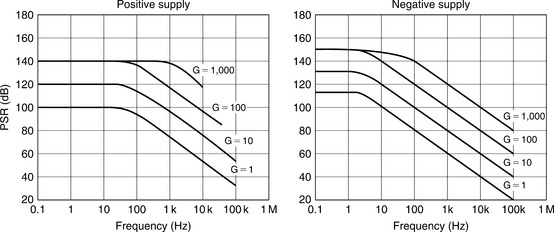
Power supply rejection (PSR) is also a function of gain and frequency. For in amps, it is customary to specify the sensitivity to each power supply separately, as shown in Figure 2-22 for the AD620. The RTI PSR error is obtained by dividing the power supply deviation from nominal by the power supply rejection ratio (PSRR).
Because of the relatively poor PSR at high frequencies, decoupling capacitors are required on both power pins to an in amp. Low inductance ceramic capacitors (0.01–0.1 μF) are appropriate for high frequencies. Low ESR electrolytic capacitors should also be located at several points on the PC board for low frequency decoupling.
Note that these decoupling requirements apply to all linear devices, including op amps and data converters. Further details on power supply decoupling are found in Chapter 7.
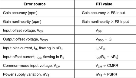
Now that all DC error sources have been accounted for, a worst-case DC error budget can be calculated by reflecting all the sources to the in amp input, as is illustrated by the table of Figure 2-23.
It should be noted that the DC errors can be referred to the in amp output (RTO) by simply multiplying the RTI error by the in amp gain.
In Amp Noise Sources
Since in amps are primarily used to amplify small precision signals, it is important to understand the effects of all the associated noise sources. The in amp noise model is shown in Figure 2-24.

There are two sources of input voltage noise. The first is represented as a noise source, VNI, in series with the input, as in a conventional op amp circuit. This noise is reflected to the output by the in amp gain, G. The second noise source is the output noise, VNO, represented as a noise voltage in series with the in amp output. The output noise, shown here referred to VOUT, can be RTI by dividing by the gain, G.
There are also two noise sources associated with the input noise currents IN+ and IN−. Even though IN+ and IN− are usually equal (IN+ ≈ IN− = IN), they are uncorrelated, and therefore, the noise they each create must be summed in a root-sum-squares (RSS) fashion. IN+ flows through one-half of RS, and IN− the other half. This generates two noise voltages, each having an amplitude INRS/2. Each of these two noise sources is reflected to the output by the in amp gain, G.
The total output noise is calculated by combining all four noise sources in an RSS manner:
 (2-6)
(2-6) (2-7)
(2-7)The total noise, RTI is simply the above expression divided by the in amp gain, G:
 (2-8)
(2-8)In amp data sheets often present the total voltage noise RTI as a function of gain. This noise spectral density includes both the input (VNI) and output (VNO) noise contributions. The input current noise spectral density is specified separately.
As in the case of op amps, the total in amp noise RTI must be integrated over the applicable in amp closed-loop bandwidth to compute an RMS value. The bandwidth may be determined from data sheet curves that show frequency response as a function of gain.
Regarding this bandwidth, some care must be taken in computing it, as it is often not constant bandwidth product relationship, as is true with VFB op amps. In the case of the AD620 in amp family, e.g., the gain-bandwidth pattern is more like that of a CFB op amp. In such cases, the safest way to predict the bandwidth at a given gain is to use the curves supplied within the data sheet.
In Amp Bridge Amplifier Error Budget Analysis
It is important to understand in amp error sources in a typical application. Figure 2-25 shows a 350 Ω load cell with a full-scale output of 100 mV when excited with a 10 V source. The AD620 is configured for a gain of 100 using the external 499 Ω gain-setting resistor. The table shows how each error source contributes to a total unadjusted error of 2,145 ppm. Note however that the gain, offset, and CMR errors can all be removed with a system calibration. The remaining errors—gain nonlinearity and 0.1–10 Hz noise—cannot be removed with calibration and ultimately limit the system resolution to 42.8 ppm (approximately 14-bit accuracy).

This example is of course just an illustration, but should be useful toward the importance of addressing performance-limiting errors such as gain nonlinearity and low frequency noise.
In Amp Input Overvoltage Protection
In their typical application as interface amplifiers for data acquisition systems, in amps are often subjected to input overloads, i.e., voltage levels in excess of the full-scale for the selected gain range. The manufacturer’s “absolute maximum” input ratings for the device should be closely observed. As with op amps, many in amps have absolute maximum input voltage specifications equal to ± VS.
In some cases, external series resistors (for current limiting) and diode clamps may be used to prevent overload, if necessary (see Figure 2-26). Some in amps have built-in overload protection circuits in the form of series resistors. For example, the AD620 series have thin-film resistors, and the substrate isolation they provide allows input voltages that can exceed the supplies. Other devices use series-protection FETs, e.g. the AMP02 and the AD524, because they act as a low impedance during normal operation, and a high impedance during overvoltage fault conditions. In any instance however, there are always finite safe limits to applied overvoltage (Figure 2-26, again).
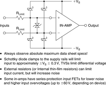
In some instances, an additional transient voltage suppressor (TVS) may be required across the input pins to limit the maximum differential input voltage. This is especially applicable to three op amp in amps operating at high gain with low values of RG.
A more detailed discussion of input overvoltage and EMI/RFI protection can be found in Chapter 11 of this book.
SECTION 2-4 Differential Amplifiers
Many high performance analog-to-digital converters (ADCs) are now being designed with differential inputs. A fully differential ADC design offers the advantages of good CM rejection, reduction in second-order distortion products, and simplified DC trim algorithms. Although they can be driven single ended, a fully differential driver usually optimizes overall performance.
One of the most common ways to drive a differential input ADC is with a transformer. However, there are many applications where the ADCs cannot be driven with transformers because the frequency response must extend to DC. In these cases, differential drivers are required.
A block diagram of the AD813X family of fully differential amplifiers optimized for ADC driving is shown in Figure 2-27 (see References 3–5). Figure 2-27(A) shows the details of the internal circuit, and Figure 2-27(B) shows the equivalent circuit. The gain is set by the external RF and RG resistors, and the

CM voltage is set by the voltage on the VOCM pin. The internal CM feedback forces the VOUT+ and VOUT− outputs to be balanced, i.e., the signals at the two outputs are always equal in amplitude but 180° out of phase as per the equation:
The circuit can be used with either a differential or a single-ended input, and the voltage gain is equal to the ratio of RF to RG.
If a buffered differential voltage output is required from a current output DAC, the AD813X-series of differential amplifiers can be used as shown in Figure 2-28.

The DAC output current is first converted into a voltage that is developed across the 25 Ω resistors. The voltage is amplified by a factor of 5 using the AD813X. This technique is used in lieu of a direct I/V conversion to prevent fast slewing DAC currents from overloading the amplifier and introducing distortion. Care must be taken so that the DAC output voltage is within its compliance rating.
The VOCM input on the AD813X can be used to set a final output CM voltage within the range of the AD813X. If transmission lines are to be driven at the output, adding a pair of 75 Ω resistors will allow this.
Note also that these amplifiers can be used with single-ended inputs as well. Grounding one of the inputs turns these amplifiers into single ended to differential converters.
SECTION 2-5 Isolation Amplifiers
Analog Isolation Techniques
There are many applications where it is desirable, or even essential, for a sensor to have no direct (“galvanic”) electrical connection with the system to which it is supplying data. This might be in order to avoid the possibility of dangerous voltages or currents from one-half of the system doing damage in the other, or to break an intractable ground loop. Such a system is said to be “isolated,” and the arrangement that passes a signal without galvanic connections is known as an isolation barrier.
The protection of an isolation barrier works in both directions, and may be needed in either, or even in both. The obvious application is where a sensor may encounter high voltages, such as monitoring the current in an AC induction motor, and the system it is driving must be protected. Or a sensor may need to be isolated from accidental high voltages arising downstream, in order to protect its environment: examples include the need to prevent the ignition of explosive gases by sparks at sensors and the protection from electric shock of patients whose ECG, EEG, or EMG is being monitored. The ECG case is interesting, as protection may be required in both directions: the patient must be protected from accidental electric shock, but if the patient’s heart should stop, the ECG machine must be protected from the very high voltages (>7.5 kV) applied to the patient by the defibrillator which will be used to attempt to restart it.
Just as interference, or unwanted information, may be coupled by electric or magnetic fields, or by electromagnetic radiation, these phenomena may be used for the transmission of wanted information in the design of isolated systems.
The most common isolation amplifiers use transformers, which exploit magnetic fields, and another common type uses small high voltage capacitors, exploiting electric fields. Optoisolators, which consist of an LED and a photocell, provide isolation by using light, a form of electromagnetic radiation. Different isolators have differing performance: some are sufficiently linear to pass high accuracy analog signals across an isolation barrier. With others, the signal may need to be converted to digital form before transmission for accuracy is to be maintained (note this is a common V/F converter application).
Transformers are capable of analog accuracy of 12–16 bits and bandwidths up to several hundred kHz, but their maximum voltage rating rarely exceeds 10 kV, and is often much lower. Capacitively coupled isolation amplifiers have lower accuracy, perhaps 12 bits maximum, lower bandwidth, and lower voltage ratings—but they are low cost. Optical isolators are fast and cheap, and can be made with very high voltage ratings (4–7 kV is one of the more common ratings), but they have poor analog domain linearity, and are not usually suitable for direct coupling of precision analog signals.
Linearity and isolation voltage are not the only issues to be considered in the choice of isolation systems. Operating power is of course, essential. Both the input and the output circuitry must be powered, and unless there is a battery on the isolated side of the isolation barrier (which is possible, but rarely convenient), some form of isolated power must be provided. Systems using transformer isolation can easily use a transformer (either the signal transformer or another one) to provide isolated power, but it is impractical to transmit useful amounts of power by capacitive or optical means. Systems using these forms of isolation must make other arrangements to obtain isolated power supplies—this is a powerful consideration in favor of choosing transformer isolated isolation amplifiers: they almost invariably include an isolated power supply.
The isolation amplifier has an input circuit that is galvanically isolated from the power supply and the output circuit. In addition, there is minimal capacitance between the input and the rest of the device. Therefore, there is no possibility for DC current flow, and minimum AC coupling. Isolation amplifiers are intended for applications requiring safe, accurate measurement of low frequency voltage or current (up to about 100 kHz) in the presence of high CM voltage (to thousands of volts) with high CMR. They are also useful for line-receiving of signals transmitted at high impedance in noisy environments, and for safety in general-purpose measurements, where DC and line-frequency leakage must be maintained at levels well below certain mandated minimums. Principal applications are in electrical environments of the kind associated with medical equipment, conventional and nuclear power plants, automatic test equipment, and industrial process control systems.
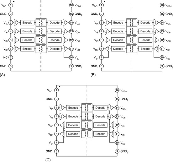
AD210 Three-Port Isolator
A basic form of isolator is the three-port isolator (input, power, output all isolated) shown in Figure 2-29. Note that in this diagram, the input circuits, output circuits, and power source are all isolated from one another. This Figure represents the circuit architecture of a self-contained isolator, the AD210 (see References 1 and 2).

An isolator of this type requires power from a two-terminal DC power supply (PWR, PWR COM). An internal oscillator (50 kHz) converts the DC power to AC, which is transformer-coupled to the shielded input section, then converted to DC for the input stage and the auxiliary power output. The output current capability of this output is typically limited to ± 15 mA.
The AC carrier is also modulated by the input stage amplifier output, transformer-coupled to the output stage, demodulated by a phase-sensitive demodulator (using the carrier as the reference), filtered, and buffered using isolated DC power derived from the carrier.
The AD210 allows the user to select gains from 1 to 100, using external resistors with the input section op amp. Bandwidth is 20 kHz, and voltage isolation is 2,500 VRMS (continuous) and ± 3,500 VPEAK (continuous).
The AD210 is a three-port isolation amplifier, thus the power circuitry is isolated from both the input and the output stages and may therefore be connected to either (or to neither), without change in functionality. It uses transformer isolation to achieve 3,500 V isolation with 12-bit accuracy.
Motor Control Isolation Amplifier
A typical isolation amplifier application using the AD210 is shown in Figure 2-30. The AD210 is used with an AD620 instrumentation amplifier in a current-sensing system for motor control. The input of the AD210, being isolated, can be directly connected to a 110 or 230 V power line without protection being necessary. The input section’s isolated ± 15 V powers the AD620, which senses the voltage drop in a small value current-sensing resistor. The AD210 input stage op amp is simply connected as a unity-gain follower, which minimizes its error contribution. The 110 or 230 VRMS CM voltage is ignored by this isolated system.

Within this system the AD620 preamp is used as the system scaling control point, and will produce an output voltage proportional to motor current, as scaled by the sensing resistor value and gain as set by the AD620’s RG. The AD620 also improves overall system accuracy, as the AD210’s VOS is 15 mV, versus the AD620’s 30 μV (with less drift also). Note that if higher DC offset and drift are acceptable, the AD620 may be omitted and the AD210 connected at a gain of 100.
Optional Noise Reduction Post Filter
Due to the nature of this type of carrier-operated isolation system, there will be certain operating situations where some residual AC carrier component will be superimposed on the recovered output DC signal. When this occurs, a low impedance passive RC filter section following the output stage may be used (if the following stage has a high input impedance, i.e., non-loading to this filter). Note that it will be the case for many high input impedance sampling ADCs, which appear essentially as small capacitors. A 150 Ω resistance and 1 nF capacitor will provide a corner frequency of about 1 kHz. Note also that the capacitor should be a film type for low errors, such as polypropylene. As an option an active filter may be utilized. Since the output of the filter is low impedance (the output of an op amp), it may be used where the low output is required. Also note that it may be possible to include the anti-aliasing requirement of the ADC into this filter.
Two-Port Isolator
A two-port isolator differs from a three-port isolator in that the power section is not isolated from the output section. The AD215 is an example of a high speed, two-port isolation amplifier, designed to isolate and amplify wide bandwidth analog signals (see Reference 3). The innovative circuit and transformer design of the AD215 ensures wide-band dynamic characteristics, while preserving DC performance specifications. An AD215 block diagram is shown in Figure 2-31.
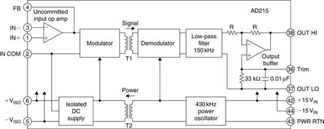
The AD215 provides complete galvanic isolation between the input and output of the device, which also includes the user-available front-end isolated bipolar power supply. The functionally complete design, powered by a ± 15 V DC supply on the output side, eliminates the need for a user supplied isolated DC/DC converter. This permits the designer to minimize circuit overhead and reduce overall system design complexity and component costs.
The AD215 has a ± 10 V input/output range, a specified gain range of 1 V/V to 10 V/V, a buffered output with offset trim and a user-available isolated front-end power supply which produces ± 15 V DC at ± 10 mA.
SECTION 2-6 Digital Isolation Techniques
While not a linear circuit, digital isolation is closely related to isolation amplifiers, so they will be discussed here.
Analog isolation amplifiers find many applications where a high isolation is required, such as in medical instrumentation. Digital isolation techniques provide similar galvanic isolation and are a reliable method of transmitting digital signals without ground noise.
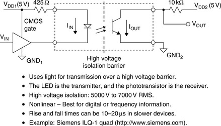
Optocouplers (also called optoisolators) are useful and available in a wide variety of styles and packages. A typical optocoupler based on an LED and a phototransistor is shown in Figure 2-32. A current of approximately 10 mA drives an LED transmitter, with light output received by a phototransistor. The light produced by the LED saturates the phototransistor. Input/output isolation of 5,000 VRMS to 7,000 VRMS is common. Although fine for digital signals, optocouplers are too nonlinear for most analog applications. In addition, the transfer characteristics of the optocoupler change with time. Also, since the phototransistor is often being saturated, response times can range from 10 to 20 μs in slower devices, limiting high speed applications.
A much faster optocoupler architecture is shown in Figure 2-33 and is based on an LED and a photodiode. The LED is again driven with a current of approximately 10 mA. This produces a light output sufficient to generate enough current in the receiving photodiode to develop a valid high logic level at the output of the transimpedance amplifier. Speed can vary widely between optocouplers, and the fastest ones have propagation delays of 20 ns typical, and 40 ns maximum, and can handle data rates up to 25 MBd for NRZ data. This corresponds to a maximum square wave operating frequency of 12.5 MHz, and a minimum allowable passable pulse width of 40 ns.

AD260/AD261 High Speed Logic Isolators
The AD260/AD261 family of digital isolators operates on a principle of transformer-coupled isolation (see Reference 4). They provide isolation for five digital control signals to/from high speed DSPs, microcontrollers, or microprocessors. The AD260 also has a 1.5 W transformer for a 3.5 kVRMS isolated external AC/DC power supply circuit.
Each line of the AD260 can handle digital signals up to 20 MHz (40 MBd) with a propagation delay of only 14 ns which allows for extremely fast data transmission. Output waveform symmetry is maintained to within ± 1 ns of the input so the AD260 can be used to accurately isolate time-based pulse width modulator (PWM) signals.
A simplified schematic of one channel of the AD260/AD261 is shown in Figure 2-34. The data input is passed through a Schmitt trigger circuit, through a latch, and a special transmitter circuit which differentiates the edges of the digital input signal and drives the primary winding of a proprietary transformer with a “set-high/set-low” signal.

The secondary of the isolation transformer drives a receiver with the same “set-high/set-low” data, which regenerates the original logic waveform. An internal circuit operating in the background interrogates all inputs about every 5 μs, and in the absence of logic transitions, sends appropriate “set-high/set-low” data across the interface. Recovery time from a fault condition or at power-up is thus between 5 μs and 10 μs.
The power transformer (available on the AD260) is designed to operate between 150 kHz and 250 kHz and will easily deliver more than 1 W of isolated power when driven push–pull (5 V) on the transmitter side. Different transformer taps, rectifier and regulator schemes will provide combinations of ±5 V, 15 V, 24 V, or even 30 V or higher.
The transformer output voltage when driven with a low voltage drop drive will be 37 Vp−p across the entire secondary with a 5 V push–pull drive. The availability of low cost digital isolators such as those previously discussed solves most system isolation problems in data acquisition systems as shown in Figure 2-35. In the upper example, digitizing the signal first and then using digital isolation eliminates the problem of analog isolation amplifiers. While digital isolation can be used with parallel output ADCs provided the bandwidth of the isolator is sufficient, it is more practical with ADCs that have serial outputs. This minimizes cost and component count. A three-wire interface (data, serial clock, framing clock) is all that is required in these cases.
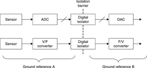
An alternative (lower example) is to use a voltage-to-frequency converter (VFC) as a transmitter and a frequency-to-voltage converter (FVC) as a receiver. In this case, only one digital isolator is required.
iCoupler® Technology
In many industrial applications, such as process control systems or data acquisition and control systems, digital signals must be transmitted from various sensors to a central controller for processing and analysis. The controller then needs to transmit commands as a result of the analysis performed, coupled with user inputs to various actuators, to achieve certain operations. To maintain safety voltage at the user interface and to prevent transients from being transmitted from the sources, galvanic isolation is required. There are three commonly known classes of isolation devices: optocouplers, capacitively coupled isolators, and transformer-based isolators. Optocouplers rely on light emitting diodes to convert the electrical signals to light signals and on photo detectors to convert the light signals back to electrical signals. The intrinsic low conversion efficiencies for electrical light conversion and slow response photo detectors lead to optocoupler limitations in terms of lifetime, speed, and power assumption. The capacitively coupled isolators have limitations in their size and ability to reject CM voltage transients, while the traditional transformer assembly based isolators are bulky and expensive. All these isolators are restricted, moreover, because of integrated circuit integration limitations and the fact that they often need hybrid packaging.
Recently iCoupler®, a new isolation technology, based on chip scale transformers, was developed by Analog Devices. The first product was the ADuM1100 single-channel digital isolator. iCoupler® technology leverages thick-film processing techniques to build microscale on-chip transformers and achieves thousands of volts of isolation on a chip.
iCoupler® isolated transformers can be monolithically integrated with standard silicon ICs and can be fabricated in single- or multichannel configurations. The bidirectional nature of inductive coupling further facilitates bidirectional signal transfer. The combination of high bandwidth for these on-chip transformers and fine-scale CMOS circuitry leads to isolators of unmatched performance characteristics in power, speed, timing accuracy, and ease of use.
ADuM1100 Architecture: A Single-Channel Digital Isolator
The ADuM1100 is a single-channel 100 Mbps digital isolator. It has two ICs packaged in an eight-lead SOIC package. A cross-section view of the ADuM1100 is shown in Figure 2-36. There are two lead frame paddles inside the package, with a gap between them of about 0.4 mm. The molding compound has breakdown strength over 25 kV/mm, so the 0.4 mm gap filled with molding compound provides greater than 10 kV insulation between the substrates of two IC chips.
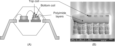
Figure 2-36: (A) Cross-sectional view of ADuM1100 in an eight-lead SOIC package. (B) Cross-sectional view of the top coil and polyimide layers
The driver chip sitting on the left paddle takes the input digital signal, encodes it, and drives the encoded differential signal through bond wires to the top coils of the transformers built on top of the receiver chip sitting on the right paddle. The driver die is a standard CMOS chip, and the receiver die is a CMOS chip with the additional structures of two polyimide layers and transformer primary coil fabricated on top of the passivation. The polyimide between the top and bottom coils is about 20 μm thick. The breakdown strength of the cured polyimide film is greater than 300 V/m, so 20 μm of polyimide provides greater than 6 kV of insulation between a given transformer’s coils. This provides a comfortable margin over the production test voltage of 3 kVRMS.
Because of the structural quality of these wafer processed polyimide films, no partial discharge over 5 pC can be detected, even at 3 kVRMS. The top coil is gold plated, with a 4-μm thick layer, and the coil track width and spacing between the turns are all 4 μm. The polyimide layers have good mechanical elongation and tensile strength, which also helps the adhesion between the polyimide layers or between the polyimide layer and deposited metal layer. The minimum interaction between the gold film and the polyimide film, coupled with high temperature stability of the polyimide film, results in a system that provides reliable insulation when subjected to various types of environmental stress.
In addition to the fact that thousands of volts of isolation can be achieved on-chip, the ADuM110 also makes it possible to transmit very high bandwidth signals very efficiently, accurately, and reliably. Figure 2-37 shows a simplified schematic of the ADuM1100. To guarantee input stability, the front glitch filter filters out pulses narrower than a pulse width of approximately 2 ns. Upon the receipt of a signal edge, a 1 ns pulse is sent to either Coil 1 or Coil 2. (For a leading edge signal it is sent to Coil 1, and for a falling edge signal to Coil 2.) Once the short pulses are transmitted to the secondary coils (the bottom coils in this case), they are amplified and the input signal is reconstructed through an SR flip-flop to appear as an isolated output. The wide bandwidth of these microscale transformers and high speed CMOS makes the transmission of these short nanosecond pulses possible. Since only signal edges are being used, this transmission scheme is very power efficient. With a very energetic pulse having a current ramping to 100 mA within 1 ns, the average current for a 1 Mbps input signal is only 50 μA. Some additional power is dissipated by the switching of the surrounded CMOS gates. At 5 V, an additional 50 μA/Mbps is needed if the total capacitance of the CMOS gates is 20 pF. The typical optocoupler, on the other hand, dissipates over 10 mA, even operating at 1 Mbps. This represents two orders of magnitude (100×) improvement in power dissipation provided by iCoupler® isolators.

If there is no input change for a certain period of time, approximately 1 μs, the monostable generates a 1 ns pulse and sends it to Coil 1 or Coil 2, depending on the input logic level. The 1 ns refreshing pulse is sent to Coil 1 if input is high and is sent to Coil 2 if input is low. This helps maintain DC correctness for the isolator because normally pulses are transmitted only on reception of a signal edge. The receiver includes a watchdog circuit that will timeout at 2 μs if it is not reset by an incoming pulse. If a timeout happens, the receiver output will return to a default safe level (logic high in the ADuM1100). The combination of refresh and watchdog functions provides the additional advantage of detecting the failure of any field device on the system side. With other isolators, this would ordinarily require the use of an extra isolated data channel.
The bandwidth of the isolator is dependent on the input filter bandwidth within. For example, 500 Mbps can be achieved with a 2 ns input filter. For the ADuM1100, we chose a signal bandwidth of 100 MBd, still 2 times faster than the fastest optocouplers. Very tight edge symmetry between input and output logic signals is also preserved due to the instantaneous nature of the inductive coupling between these microscale on-chip coils.
The ADuM1100 has edge symmetry of better than 2 ns for 5 V operation. As the bandwidth of isolation systems continues to expand, the iCoupler® technology will be capable of meeting the challenge while optocoupler technology is likely to struggle.
In addition to the improvements in efficiency and bandwidth iCoupler® technology provides, it also offers a more robust and reliable isolation solution than competitive offerings. Because high voltage transients are present in many data acquisition and control systems, the ability of the isolator to prevent transients from affecting the logic controller is very important. High performance optocouplers have transient immunity of less than 10 kV/μs, while the ADuM1100 has a transient immunity better than 25 kV/μs. The induced error voltage at the receiver input induced by an input–output transient is given by:
where C is the capacitance between the input coil and the receiver coil, R, is the resistance of the bottom coil, and dV/dt is the magnitude of the transient.
In the ADuM1100, the capacitance between the top (input) coil and the bottom (receiver) coil is only 0.2 pF, while the bottom coil has a resistance of 80 Ω. Thus the error signal induced on the bottom coil by a 25 kV/μs transient on the top coil is only 0.4 V, much less than the receiver detection threshold. The transient immunity of iCoupler® isolators can be optimized through careful selection of the decoder detection threshold, the resistance of the receiving coil, and, of course, the capacitance between the top and bottom coils.
One recurring question about transformer-based isolators involves their magnetic immunity capability. Since iCouplers® use air core technology, no magnetic components are present and the problem of magnetic saturation for the core material does not exist. Therefore, iCouplers® have essentially infinite DC field immunity. The limitation on the ADuM1100’s AC magnetic field immunity is set by the condition in which the induced error voltage in the receiving coil (the bottom coil in this case) is made sufficiently large, either to falsely set or reset the decoder. The voltage induced across the bottom coil is given by:
where β is the magnetic flux density (Gauss), N is the number of turns in receiving coil, and rn is the radius of nth turn in receiving coil (cm).
Because of the very small geometry of the receiving coil in the ADuM1100, even a wire carrying 1,000A at 1 MHz and positioned only 1 cm away from the ADuM1100 would not induce an error voltage large enough to falsely trigger the decoder. Note that at combinations of strong magnetic field and high frequency, any loops formed by printed circuit board traces could induce error voltages sufficiently large to trigger the thresholds of succeeding circuitry. Typically the PC board design rather than the isolator itself is the limiting factor in the presence of such big magnetic transients. In addition to magnetic immunity, the level of electromagnetic radiation emitted from the iCoupler® device is a concern. Using far-field approximation,
where P is the total radiated power and I is the coil loop current.
Again, given the very small geometry of the coils, the total radiated power is still less than 50 pW, even if the part is operating at 0.5 GHz.
ADuM130x/ADuM140x: Multichannel Products
In addition to the many performance improvements discussed previously, iCoupler® technology also offers tremendous advantages in terms of integration. The optical interference makes the realization of multichannel optocouplers very difficult.
Transformers based on iCoupler® technology can be easily integrated onto a single chip. Furthermore, one data channel can transmit signals in one direction, say from the top coil to the bottom coil, while the neighboring channel can transmit a signal in the other direction, from the bottom coil to the top coil. The bidirectional nature of inductive coupling makes this possible.
Additional products consist of five three-channel and four-channel products covering all possible channel directionality configurations. Besides providing flexible channel configurations, they support both 3 V and 5 V operations at either side of the isolation barrier and support the use of these isolators as level translators. One side could be at 2.7 V, e.g., while the other side could be at 5.5 V. The edge symmetry of 2 ns is preserved over all possible supply configurations at all temperatures from −40°C to 100°C. The ability to mix bidirectional channels of isolation in a single package enables users to reduce the size and cost of their systems.
For the ADuM1100, two transformers are used to transmit a single channel of data. One is dedicated to transmit pulses representing the signal’s leading edge or updating input high, and the other is dedicated to transmit pulses representing the signal’s falling edge or updating input low. For the ADuM130x/ADuM140x product family, a single transformer is used for each data channel. The ADuM140x shown in Figure 2-38 has four transformers in total. The leading edge and falling edge are encoded differently, and the encoded pulses are combined in the same transformer; as a result, the receiver has responsibility for decoding the pulses to see whether they are for leading edge or falling edge. The output signal is then reconstructed correspondingly (Figure 2-39).

Of course, there is a penalty for using a single transformer per data channel rather than using two transformers per data channel. The propagation delay is longer for the single transformer architecture because of the additional encode and decode time needed. The penalty for bandwidth is hardly a factor, even at input speed of 100 Mbps.
In contrast to the ADuM1100, the ADuM130x/ADuM140x uses a dedicated transformer chip, separate from the receiver integrated circuit. This partitioning exemplifies the ease of integration for iCoupler technology. Besides standalone multichannel isolators, the iCoupler technology can be embedded with other data acquisition and control ICs to make the use of isolation even more transparent. Consequently, in the future, system designers will be able to devote their time to improving system functionality, rather than worrying about isolation.
SECTION 2-7 Active Feedback Amplifiers
The AD8129/AD8130 differential line receivers, along with their predecessor the AD830, utilize a novel amplifier topology called active feedback (see Reference 8). A simplified block diagram of these devices is shown in Figure 2-40.
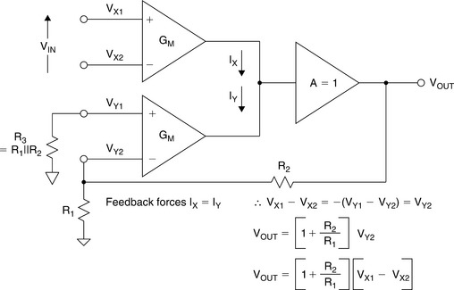
The AD830 and the AD8129/AD8130 have two sets of fully differential inputs, available at VX1−VX2 and VY1−VY2, respectively. Internally, the outputs of the two GM stages are summed and drive a buffer output stage.
In this device the overall feedback loop forces the internal currents IX and IY to be equal. This condition forces the differential voltages VX1−VX2 and VY1−VY2 to be equal and opposite in polarity. Feedback is taken from the output back to one input differential pair, while the other pair is driven directly by an input differential input signal.
An important point of this architecture is that high CM rejection is provided by the two differential input pairs, so CMR is not dependent on resistor bridges and their associated matching problems. The inherently wideband balanced circuit and the quasi-floating operation of the driven input provide the high CMR, which is typically 100 dB at DC.
One way to view this topology is as a standard op amp in a non-inverting mode with a pair of differential inputs in place of the op amps standard inverting and non-inverting inputs. The general expression for the stage’s gain “G” is like a non-inverting op amp, or:
As should be noted, this expression is identical to the gain of a non-inverting op amp stage, with R2 and R1 in analogous positions.
The AD8129 is a low noise high gain (G = 10 or greater) version of this family, intended for applications with very long cables where signal attenuation is significant. The related AD8130 device is stable at a gain of one. It is used for those applications where lower gains are required, such as a gain of two, for driving source and load terminated cables.
The AD8129 and AD8130 have a wide power supply range, from single + 5 V to ± 12 V, allowing wide CM and differential-mode voltage ranges. The wide CM range enables the driver/receiver pair to operate without isolation transformers in many systems where the ground potential difference between driver and receiver locations is several volts. Both devices include a logic-controlled power-down function.
Both devices have high, balanced input impedances, and achieve 70 dB CMR @ 10 MHz, providing excellent rejection of high frequency CM signals. Figure 2-41 shows AD8130 CMR for various supplies. As can be noted, it can be as high as 95 dB at 1 MHz, an impressive figure considering that no trimming is required.

The typical 3 dB bandwidth for the AD8129 is 200 MHz, while the 0.1 dB bandwidth is 30 MHz in the SOIC package, and 50 MHz in the μSOIC package. The conditions for these specifications are for VS = ±5 V and G = 10.
The typical 3 dB bandwidth for the AD8130 is 270 MHz, and the 0.1 dB bandwidth is 45 MHz, in either package. The conditions for these specifications are for VS = ±5 V and G = 1. Typical differential gain and phase specifications for the AD8130 for G = 2, VS = ±5 V, and RL = 150 Ω are 0.13% and 0.15°, respectively.
SECTION 2-8 Logarithmic Amplifiers
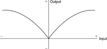
The term “logarithmic amplifier” (generally abbreviated to “log amp”) is something of a misnomer, and “logarithmic converter” would be a better description. The conversion of a signal to its equivalent logarithmic value involves a nonlinear operation, the consequences of which can be confusing if not fully understood. It is important to realize that many of the familiar concepts of linear circuits are irrelevant to log amps. For example, the incremental gain of an ideal log amp approaches infinity as the input approaches zero, and a change of offset at the output of a log amp is equivalent to a change of amplitude at its input—not a change of input offset.
For the purposes of simplicity in our initial discussions, we shall assume that both the input and the output of a log amp are voltages, although there is no particular reason why logarithmic current, transimpedance, or transconductance amplifiers could not also be designed.
If we consider the equation y = log(x) we find that every time x is multiplied by a constant A, y increases by another constant A1. Thus if log(K) = K1, then log(AK) = K1 + A1, log(A2K) = K1 + 2A1, and log(K/A) = K1−A1. This gives a graph as shown in Figure 2-42, where y is zero when x is unity, y approaches minus infinity as x approaches zero, and where y has no values for which x is negative.

On the whole, log amps do not behave in this way. Apart from the difficulties of arranging infinite negative output voltages, such a device would not, in fact, be very useful. A log amp must satisfy a transfer function of the form:
 (2-14)
over some range of input values which may vary from 100:1 (40 dB) to over 1,000,000:1 (120 dB).
With inputs very close to zero, log amps cease to behave logarithmically, and most then have a linear VIN/VOUT law. This behavior is often lost in device noise. Noise often limits the dynamic range of a log amp. The constant, VY, has the dimensions of voltage, because the output is a voltage. The input, VIN, is divided by a voltage, VX, because the argument of a logarithm must be a simple dimensionless ratio.
A graph of the transfer characteristic of a log amp is shown in Figure 2-43. The scale of the horizontal axis (the input) is logarithmic, and the ideal transfer characteristic is a straight line. When VIN = VX, the logarithm is zero (log 1 = 0). VX is therefore known as the intercept voltage of the log amp because the graph crosses the horizontal axis at this value of VIN.

The slope of the line is proportional to VY. When setting scales, logarithms to the base 10 are most often used because this simplifies the relationship to decibel values: when VIN = 10 VX, the logarithm has the value of 1, so the output voltage is VY. When VIN = 100 VX, the output is 2 VY, and so forth. VY can therefore be viewed either as the “slope voltage” or as the “volts per decade factor.”
The logarithm function is indeterminate for negative values of x. Log amps can respond to negative inputs in three different ways: (1) They can give a full-scale negative output as shown in Figure 2-44. (2) They can give an output which is proportional to the log of the absolute value of the input and disregards its sign as shown in Figure 2-45. This type of log amp can be considered to be a full-wave detector with a logarithmic characteristic and is often referred to as a detecting log amp. (3) They can give an output which is proportional to the log of the absolute value of the input and has the same sign as the input as shown in Figure 2-46. This type of log amp can be considered to be a video amp with a logarithmic characteristic, and may be known as a logarithmic video (log video) amplifier or, sometimes, a true log amp (although this type of log amp is rarely used in video-display-related applications).


There are three basic architectures which may be used to produce log amps: the basic diode log amp, the successive detection log amp, and the true log amp which is based on cascaded semi-limiting amplifiers. The successive detection log amp and the true log amp are discussed in the RF/IF section.
The voltage across a silicon diode is proportional to the logarithm of the current through it. If a diode is placed in the feedback path of an inverting op amp, the output voltage will be proportional to the log of the input current as shown in Figure 2-47. In practice, the dynamic range of this configuration is limited to 40–60 dB because of non-ideal diode characteristic, but if the diode is replaced with a diode-connected transistor as shown in Figure 2-48, the dynamic range can be extended to 120 dB or more. This type of log amp has three disadvantages: (1) both the slope and intercept are temperature dependent; (2) it will only handle unipolar signals; and (3) its bandwidth is both limited and dependent on signal amplitude.


Where several such log amps are used on a single chip to produce an analog computer which performs both log and antilog operations, the temperature variation in the log operations is unimportant, since it is compensated by a similar variation in the antilogging. This makes possible the AD538 (Figure 2-49), a monolithic analog computer which can multiply, divide, and raise to powers. Where actual logging is required, however, the AD538 and similar circuits require temperature compensation (Reference 7). The major disadvantage of this type of log amp for high frequency applications, though, is its limited frequency response—which cannot be overcome. However carefully the amplifier is designed, there will always be a residual feedback capacitance, CC (often known as Miller capacitance), from output to input which limits the high frequency response.

What makes this Miller capacitance particularly troublesome is that the impedance of the emitter–base junction is inversely proportional to the current flowing in it—so that if the log amp has a dynamic range of 1,000,000:1, then its bandwidth will also vary by 1,000,000:1. In practice, the variation is less because other considerations limit the large signal bandwidth, but it is very difficult to make a log amp of this type with a small signal bandwidth greater than a few hundred kHz.
We also discuss high speed log amps in the RF/IF section (Section 4-4).
SECTION 2-9 High Speed Clamping Amplifiers
There are many situations where it is desirable to clamp the output of an op amp to prevent overdriving the circuitry which follows. Specially designed high speed, fast recovery clamping amplifiers offer an attractive alternative to designing external clamping/protection circuits. The AD8036/AD8037’s low distortion, wide bandwidth clamp amplifiers represent a significant breakthrough in this technology. These devices allow the designer to specify a high (VH) and low (VL) clamp voltage. The output of the device clamps when the input exceeds either of these two levels. The AD8036/AD8037 offers superior clamping performance compared to competing devices that use output clamping. Recovery time from overdrive is less than 5 ns.
The key to the AD8036 and AD8037’s fast, accurate clamp and amplifier performance is their proprietary input clamp architecture. This new design reduces clamp errors by more than 10× over previous output clamp-based circuits, as well as substantially increasing the bandwidth, precision, and versatility of the clamp inputs.
Figure 2-50 shows an idealized block diagram of the AD8036 connected as a unity-gain voltage follower. The primary signal path comprises A1 (a 1,200 V/μs, 240 MHz high voltage gain, differential to single-ended amplifier) and A2 (a G = +1 high current gain output buffer). The AD8037 differs from the AD8036 only in that A1 is optimized for closed-loop gains of two or greater.

The input clamp section is composed of comparators CH and CL, which drive switch S1 through a decoder. The unity-gain buffers in series with the +VIN, VH, and VL inputs isolate the input pins from the comparators and S1 without reducing bandwidth or precision.
The two comparators have about the same bandwidth as A1 (240 MHz), so they can keep up with signals within the useful bandwidth of the AD8036. To illustrate the operation of the input clamp circuit, consider the case where VH is referenced to +1 V, VL is open, and the AD8036 is set for a gain of + 1 by connecting its output back to its inverting input through the recommended 140 Ω feedback resistor. Note that the main signal path always operates closed loop, since the clamping circuit only affects A1’s non-inverting input.
If a 0 V to +2 V voltage ramp is applied to the AD8036’s +VIN for the connection just described, VOUT should track + VIN perfectly up to + 1 V, then should limit at exactly + 1 V as + VIN continues to + 2 V.
In practice, the AD8036 comes close to this ideal behavior. As the + VIN input voltage ramps from zero to 1 V, the output of the high limit comparator CH starts in the off state, as does the output of CL. When + VIN just exceeds VH (practically, by about 18 mV), CH changes state, switching S1 from “A” to “B” reference level. Since the + input of A1 is now connected to VH, further increases in + VIN have no effect on the AD8036’s output voltage. The AD8036 is now operating as a unity-gain buffer for the VH input, as any variation in VH, for VH > 1 V, will be faithfully produced at VOUT.
Operation of the AD8036 for negative input voltages and negative clamp levels on VL is similar, with comparator CL controlling S1. Since the comparators see the voltage on the + VIN pin as their common reference level, the voltage VH and VL are defined as “High” or “Low” with respect to + VIN. For example, if VIN is set to 0 V, VH is open, and VL is +1 V, comparator CL will switch S1 to “C,” so the AD8036 will buffer the voltage on VL and ignore + VIN.
The performance of the AD8036/AD8037 closely matches the ideal just described. The comparator’s threshold extends from 60 mV inside the clamp window defined by the voltages on VL and VH to 60 mV beyond the window’s edge. Switch S1 is implemented with current steering, so that A1’s + input makes a continuous transition from, say, VIN to VH as the input voltage traverses the comparator’s input threshold from 0.9 V to 1.0 V for VH = 1.0 V.
The practical effect of the non-ideal operation is to soften the transition from amplification to clamping modes, without compromising the absolute clamp limit set by the input clamping circuit. Figure 2-51 shows a graph of VOUT versus VIN for the AD8036 and a typical output clamp amplifier. Both amplifiers are set for G = + 1 and VH = + 1 V.

The worst-case error between VOUT (ideally clamped) and VOUT (actual) is typically 18 mV times the amplifier closed-loop gain. This occurs when VIN equals VH (or VL). As VIN goes above and/or below this limit, VOUT will stay within 5 mV of the ideal value.
In contrast, the output clamp amplifier’s transfer curve typically will show some compression starting at an input of 0.8 V, and can have an output voltage as far as 200 mV over the clamp limit. In addition, since the output clamp causes the amplifier to operate open loop in the clamp mode, the amplifier’s output impedance will increase, potentially causing additional errors, and the recovery time is significantly longer.
It is important that a clamped amplifier such as the AD8036/AD8037 maintain low levels of distortion when the input signals approach the clamping voltages. Figure 2-52 shows the second and third harmonic distortions for the amplifiers as the output approaches the clamp voltages. The input signal is 20 MHz, the output signal is 2 V peak-to-peak, and the output load is 100 Ω.

Figure 2-52: AD8036/AD8037 distortion near clamping region, output = 2 Vp−p, load = 100 Ω, f = 20 MHz
Recovery from step voltage which is two times over the clamping voltage is shown in Figure 2-53. The input step voltage starts at + 2 V and goes to 0 V (left-hand traces on scope photo). The input clamp voltage (VH) is set at + 1 V. The right-hand trace shows the output waveform.

Figure 2-54 shows the AD9002 8-bit, 125 MSPS flash converter driven by the AD8037 (240 MHz bandwidth) clamping amplifier. The clamp voltages on the AD8037 are set to +0.55 and −0.55 V, referenced to the ±0.5 V input signal, with the external resistive dividers. The AD8037 also supplies a gain of two, and an offset of −1 V (using the AD780 voltage reference), to match the 0 to −2 V input range of the AD9002 flash converter. The output signal is clamped at +0.1 V and −2.1 V. This multi-function clamping circuit therefore performs several important functions as well as preventing damage to the flash converter which occurs if its input exceeds +0.5 V, thereby forward biasing the substrate diode. The 1N5712 Schottky diode adds further protection during power-up.

The feedback resistor, R2 = 301 Ω, is selected for optimum bandwidth as per the data sheet recommendation. For a gain of two, the parallel combination of R1 and R3 must also equal R2:
In addition, the Thevenin equivalent output voltage of the AD780 +2.5 V reference and the R3/R1 divider must be +1 V to provide the −1 V offset at the output of the AD8037:
Solving the equations yields R1 = 499 Ω, R3 = 750 Ω (using the nearest 1% standard resistor values).
Other input and output voltages ranges can be accommodated by appropriate changes in the external resistors.
Further examples of applications of these fast clamping op amps are given in Reference 9.
SECTION 2-10 Comparators
A comparator is similar to an op amp. It has two inputs, inverting and non-inverting, and an output. But it is specifically designed to compare the voltages between its two inputs. Therefore it operates in a nonlinear fashion. The comparator operates open loop, providing a two-state logic output voltage. These two states represent the sign of the net difference between the two inputs (including the effects of the comparator input offset voltage). Therefore, the comparator’s output will be a logic “1” if the input signal on the non-inverting input exceeds the signal on the inverting input (plus the offset voltage, VOS) and a logic “0” for the opposite case. A comparator is normally used in applications where some varying signal level is compared to a fixed level (usually a voltage reference). Since it is, in effect, a 1-bit ADC, the comparator is a basic element in all ADCs (see Figure 2-55).

Comparator DC specifications are similar to those of op amps: input offset voltage, input bias current, offset and drift, CM input range, gain, CMR, and PSR. Standard logic-related DC, timing, and interface specs are associated with the comparator outputs.
The key comparator AC specification is propagation delay: it is the time required for the output to reach the 50% point of a transition, after the differential input signal crosses the offset voltage—when driven by a square wave (typically 100 mV in amplitude) to a prescribed value of input overdrive (usually 5 mV or 10 mV).
The propagation delay in practical comparators decreases somewhat as the input overdrive is increased. This variation in propagation delay as a function of overdrive is called dispersion (see Figures 2-56 and 2-57).


The addition of hysteresis, which is application of a small amount of positive feedback, to a comparator’s transfer function is often useful in a noisy environment, or where it is undesirable for the comparator to toggle continuously between states when the input signal is at or near the switching threshold. This is true when a relatively slowly changing input is compared to a DC level. Noise can cause the output to toggle between the output levels many times. The transfer function for a comparator with hysteresis is shown in Figure 2-58.
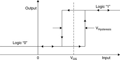
If the input voltage approaches the switching threshold (VOS) from the negative direction, the comparator will switch from a “0” to a “1” when the input crosses VOS + VH/2. The “new” switching threshold now becomes VOS−VH/2. The comparator output will remain in a “1” state until the threshold VOS−VH/2 is crossed, coming from the positive direction. Input noise centered around VOS will not cause the comparator to switch states unless it exceeds the region bounded by VOS ± VH/2.
Hysteresis can be accomplished with two resistors (see Figure 2-59); the amount of hysteresis is proportional to the resistors ratio. The signal input to the comparator may be applied to either the inverting or the non-inverting input, but if it is applied to the inverting input its source impedance must be low enough to have insignificant effect on R1 (of course if the source impedance is sufficiently predictable it may be used as R1).

If the trip voltage is midway between the two comparator output voltages (as is the case with a symmetrical power supply and a ground reference), then the introduction of hysteresis will move the positive and negative thresholds equal distances from the trip point voltage, but if the trip point is nearer to one output than to the other the thresholds will be asymmetrically placed about the trip point voltage (Figure 2-60).

To calculate the hysteresis, assume the comparator output voltages are Vp and Vn respectively. The comparator trip point voltage is VOS. The negative threshold is:
And the positive threshold voltage is:
A problem encountered with external hysteresis is that output voltage depends on supply voltage and loading. This means the hysteresis voltage can vary from application to application; though this affects resolution, it need not be a serious problem, since the hysteresis is usually a very small fraction of the range and can tolerate a safety margin of two or three (or more) times what one might calculate. Swapping in a few comparators can help confidence in the safety margin. Do not use wirewound resistors for feedback; their inductance can make matters worse.
Some comparators have hysteresis built in. An example of this is the AD790 (see Figure 2-61). The hysteresis voltage is nominally 500 μV. This, of course, can be overridden by applying external hysteresis.

The AD790 has an additional advantage. The supplies on the input (analog) side are not necessarily those on the output. The output swing is from VLOGIC to GND. The input supplies can be ± 15 V down to + 5 V and Ground.
It is quite common for the output of a comparator to be open collector (open drain). This allows interfacing to whatever logic level is appropriate to the following circuitry. Note that the maximum allowable output voltage must be observed, but this is usually not too great an issue.
A window comparator makes use of two comparators with different reference voltages and a common input voltage. The comparators are connected to logic in such a way that the final output logic level is asserted when the input signal falls between the two reference voltages (Figure 2-62).

Many comparators have an internal latch. The latch-enable signal has two states: compare (track) and latch (hold). When the latch-enable signal is in the compare state, the comparator output continuously responds to the sign of the net differential input signal. When the latch-enable signal transitions to the latch state, the comparator output goes to either a logic “1” or a logic “0,” depending on the sign of the differential input signal at the instant of the transition (at this point, we are neglecting the setup and hold-time, as well as the output propagation delay associated with the latch-enable function). Even though many comparators have a latch-enable function, they are often operated only in the compare mode.
The comparator internal latch-enable function is particularly useful in ADC applications because it allows the comparator decision to be recorded at a known instant of time. Flash converters make use of this concept and are constructed of many parallel comparators which share a common latch-enable line. Typical timing associated with the latch-enable function is shown in Figure 2-63. The delay between the assertion of latch-enable and the 50% point of the output logic swing is referred to as latch-enable to output delay. It may be different for positive- and negative-going outputs. The other key specification associated with the latch-enable function is the minimum allowable latch-enable pulse width. This specification determines the maximum frequency at which the comparator can be strobed.
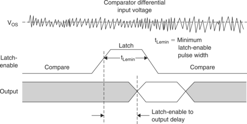
Fast comparators are somewhat difficult to apply because of their high gain and bandwidth. Proper application of high speed layout, grounding, decoupling, and signal routing is mandatory when using comparators. This cannot be over-emphasized. The biggest problem is their tendency to oscillate when the input signal is very near to or equal to the switching threshold. This can also happen when a slow signal is compared to a DC reference. Hysteresis and the use of a narrow latch-enable pulse will generally help these conditions. TTL comparators are more likely to oscillate than ECL ones because of their large output swings and fast edges, often combined with power supply current spikes as the output changes state. This can feedback to the input in the form of noise.
Using Op Amps as Comparators
Even though op amps and comparators may seem interchangeable at first glance, there are some important differences.
Comparators are designed to work open loop; they are designed to drive logic from their outputs; and they are designed to work at high speed with minimal instability. Op amps are not designed for use as comparators; they may saturate if over-driven which may cause them to recover comparatively slowly. Many have input stages which behave in unexpected ways when used with large differential voltages; in fact, in many cases, the differential input voltage range of the op amp is limited. And op amp outputs are rarely compatible with logic.
Yet many people still try to use op amps as comparators. While this may work at low speeds and low resolutions, many times the results are not satisfactory. Not all of the issues involved with using an op amp as a comparator can be resolved by reference to the op amp data sheet, since op amps are not intended for use as comparators.
The most common issues are speed (as we have already mentioned), the effects of input structures (protection diodes, phase inversion in FET amplifiers, and many others), output structures which are not intended to drive logic, hysteresis and stability, and CM effects.
Speed
Most comparators are quite fast, but so are some op amps. Why must we expect low speed when using an op amp as a comparator?
A comparator is designed to be used with large differential input voltages, whereas op amps normally operate with their differential input voltage minimized by negative feedback. When an op amp is overdriven, sometimes by only a few millivolts, some of its stages may saturate. If this occurs the device will take a comparatively long time to come out of saturation and will therefore be much slower than if it always remained unsaturated (Figure 2-64).

The time to come out of saturation of an overdriven op amp is likely to be considerably longer than the normal group delay of the amplifier, and will often depend on the amount of overdrive. Because few op amps have this desaturation time specified for various amounts of overdrive, it will generally be necessary to determine, by experiment, the behavior of the amplifier under the conditions of overdrive to be expected in a particular application.
The results of such experiments should be regarded with suspicion and the values of propagation delay through the op amp comparator which is chosen for worst-case design calculations should be at least twice the worst value seen in any experiment.
Output Considerations
The output of a comparator will be designed to drive a particular logic family or families, while the output of an op amp is designed to swing from supply rail to supply rail.
Frequently the logic being driven by the op amp comparator will not share the op amp’s supplies and the op amp rail-to-rail swing may go outside the logic supply rails—this will probably destroy the logic circuitry, and the resulting short-circuit may destroy the op amp as well.
There are three types of logic which we must consider: ECL, TTL, and CMOS.
ECL is a very fast current steering logic family. It is unlikely that an op amp would be used as a comparator in applications where ECL’s highest speed is involved, for reasons given above, so we will usually be concerned only to drive ECL logic levels from an op amp’s signal swing, and some additional loss of speed due to stray capacities will be unimportant. To do this we need only three resistors, as shown in Figure 2-65.

R1, R2, and R3 are chosen so that when the op amp output is positive the level at the gate is −0.8 V, and when it is low it is −1.6 V. ECL is occasionally used with positive, rather than negative, supplies (i.e., the other rail is connected to ground); the same basic interface circuit may be used but the values must be recalculated.
Although CMOS and TTL input structures, logic levels, and current flows are quite different (although some CMOS is specified to work with TTL input levels), the same interface circuitry will work perfectly well with both types of logic, since they both work for logic 0 near to 0 V and logic 1 near to 5 V.
The simplest interface uses a single N-channel MOS transistor and a pull-up resistor, RL. A similar circuit may be made with an NPN transistor, RL, and an additional transistor and diode (Figure 2-66). These circuits are simple, inexpensive, and reliable, and may be connected with several transistors in parallel and a single RL to give a “wired-or” function, but the speed of the 0–1 transition depends on the value of RL and the stray capacity of the output node. The lower the value of RL the faster, but the higher, the power consumption. By using two MOS devices, one P-channel and one N-channel, it is possible to make a CMOS/TTL interface using only two components which have no quiescent power consumption in either state.

Furthermore, it may be made inverting or non-inverting by simple positioning of components. It does, however, have a large current surge during switching, when both devices are on at once, and unless MOS devices with high channel resistance are used, a current-limiting resistor may be necessary to reduce this effect. It is also important, in this application and the one in Figure 2-67, to use MOS devices with gate-source breakdown voltages, VBGS, greater than the output voltages of the comparator in either direction. A value of VBGS > ± 25 V is common in MOS devices and is usually adequate, but many MOS devices contain gate protection diodes which reduce the value—these should not be used.

Input Circuitry
There are a number of effects which must be considered regarding the inputs of op amps used as comparators. The first-level assumption engineers make about all op amps and comparators is that they have infinite input impedance and can be regarded as open circuits (except for current feedback (transimpedance) op amps, which have a high impedance on their non-inverting input but a low impedance of a few tens of Ω on their inverting input).
But many op amps (especially bias-compensated ones such as the OP-07 and its many descendants) contain protective circuitry to prevent large voltages damaging input devices (Figure 2-68).

Others contain more complex input circuitry, which only has high impedance when the differential voltage applied to it is less than a few tens of mV, or which may actually be damaged by differential voltages of more than a few volts. It is therefore necessary, when using an op amp as a comparator, to study the data sheet to determine how the input circuitry behaves when large differential voltages are applied to it. (It is always necessary to study the data sheet when using an integrated circuit to ensure that its non-ideal behavior (and every integrated circuit ever made has some non-ideal behavior) is compatible with the proposed application—it is just more important than usual in the present case.)
Of course some comparator applications never involve large differential voltages—or if they do the comparator input impedance when large differential voltages are present is comparatively unimportant. In such cases it may be appropriate to use as a comparator an op amp whose input circuitry behaves nonlinearly—but the issues involved must be considered, not just ignored.
As mentioned elsewhere, nearly all BIFET op amps exhibit anomalous behavior when their inputs are close to one of their supplies (usually the negative supply). Their inverting and non-inverting inputs may become interchanged. If this should occur when the op amp is being used as a comparator, the phase of the system involved will be inverted, which could well be inconvenient. The solution is, again, careful reading of the data sheet to determine just what CM range is acceptable.
Also, absence of negative feedback means that, unlike that of op amp circuits, the input impedance is not multiplied by the loop gain. As a result, the input current varies as the comparator switches. Therefore the driving impedance, along with parasitic feedbacks, can play a key role in affecting circuit stability. While negative feedback tends to keep amplifiers within their linear region, positive feedback forces them into saturation.
SECTION 2-11 Analog Multipliers
A multiplier is a device having two input ports and an output port. The signal at the output is the product of the two input signals. If both input and output signals are voltages, the transfer characteristic is the product of the two voltages divided by a scaling factor, K, which has the dimension of voltage (see Figure 2-69). From a mathematical point of view, multiplication is a “four-quadrant” operation—that is to say that both inputs may be either positive or negative and the output can be positive or negative. Some of the circuits used to produce electronic multipliers, however, are limited to signals of one polarity. If both signals must be unipolar,

we have a “single-quadrant” multiplier, and the output will also be unipolar. If one of the signals is unipolar, but the other may have either polarity, the multiplier is a “two-quadrant” multiplier, and the output may have either polarity (and is “bipolar”). The circuitry used to produce one- and two-quadrant multipliers may be simpler than that required for four-quadrant multipliers, and since there are many applications where full four-quadrant multiplication is not required, it is common to find accurate devices which work only in one or two quadrants. An example is the AD539, a wideband dual two-quadrant multiplier which has a single unipolar VY input with a relatively limited bandwidth of 5 MHz, and two bipolar VX inputs, one per multiplier, with bandwidths of 60 MHz (Figure 2-70). A block diagram of the AD539 is shown in Figure 2-71.
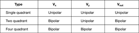
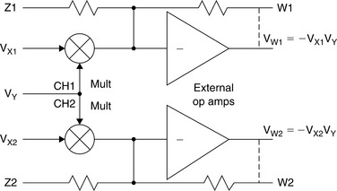
The simplest electronic multipliers use logarithmic amplifiers. The computation relies on the fact that the antilog of the sum of the logs of two numbers is the product of those numbers (see Figure 2-72).

The disadvantages of this type of multiplication are the very limited bandwidth and single-quadrant operation. A far better type of multiplier uses the “Gilbert Cell.” This structure was invented by Barrie Gilbert, now of Analog Devices, in the late 1960s (see References 1 and 2).
There is a linear relationship between the collector current of a silicon junction transistor and its transconductance (gain) which is given by:
where Ic = the collector current, Vbe = the base–emitter voltage, q = the electron charge (1.60219 × 10⁻¹⁹), k = Boltzmann’s constant (1.38062 × 10⁻²³), and T = the absolute temperature.
This relationship may be exploited to construct a multiplier with a differential (long-tailed) pair of silicon transistors, as shown in Figure 2-73.
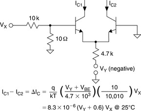
This is a rather poor multiplier because (1) the Y input is offset by the VBE—which changes nonlinearly with VY; (2) the X input is nonlinear as a result of the exponential relationship between Ic and VBE; and (3) the scale factor varies with temperature.
Gilbert realized that this circuit could be linearized and made temperature stable by working with currents, rather than voltages, and by exploiting the logarithmic Ic/VBE properties of transistors (see Figure 2-74). The

X input to the Gilbert Cell takes the form of a differential current, and the Y input is a unipolar current. The differential X currents flow in two diode-connected transistors, and the logarithmic voltages compensate for the exponential VBE/Ic relationship. Furthermore, the q/kT scale factors cancel. This gives the Gilbert Cell the linear transfer function,
As it stands, the Gilbert Cell has three inconvenient features: (1) its X input is a differential current; (2) its output is a differential current; and (3) its Y input is a unipolar current—so the cell is only a two-quadrant multiplier.
By cross-coupling two such cells and using two voltage-to-current converters (as shown in Figure 2-75), we can convert the basic architecture to a four-quadrant device with voltage inputs, such as the AD534. At low and medium frequencies, a subtractor amplifier may be used to convert the differential current at the output to a voltage. Because of its voltage output architecture, the bandwidth of the AD534 is only about 1 MHz, although the AD734, a later version, has a bandwidth of 10 MHz.

Figure 2-75: A multiplier and an op amp configured as a divider in both inverting and non-inverting modes
In Figure 2-75, Q1A and Q1B, and Q2A and Q2B form the two core long-tailed pairs of the two Gilbert Cells, while Q3A and Q3B are the linearizing transistors for both cells. In Figure 2-75 there is an operational amplifier acting as a differential current to single-ended voltage converter, but for higher speed applications, the cross-coupled collectors of Q1 and Q2 form a differential open collector current output (as in the AD834 500 MHz multiplier).
The translinear multiplier relies on the matching of a number of transistors and currents. This is easily accomplished on a monolithic chip. Even the best IC processes have some residual errors, however, and these show up as four DC error terms in such multipliers. In early Gilbert Cell multipliers, these errors had to be trimmed by means of resistors and potentiometers external to the chip, which was somewhat inconvenient. With modern analog processes, which permit the laser trimming of SiCr thin-film resistors on the chip itself, it is possible to trim these errors during manufacture so that the final device has very high accuracy. Internal trimming has the additional advantage that it does not reduce the high frequency performance, as may be the case with external trimpots.
Because the internal structure of the translinear multiplier is necessarily differential, the inputs are usually differential as well (after all, if a single-ended input is required it is not hard to ground one of the inputs). This is not only convenient in allowing CM signals to be rejected, it also permits more complex computations to be performed. The AD534 (shown previously in Figure 2-71) is the classic example of a four-quadrant multiplier based on the Gilbert Cell. It has an accuracy of 0.1% in the multiplier mode, fully differential inputs, and a voltage output. However, as a result of its voltage output architecture, its bandwidth is only about 1 MHz.
Multipliers can be placed in the feedback loop of op amps to form several useful functions. Figure 2-76 illustrates the basic principle of analog computation that a function generator in a negative feedback loop computes the inverse function (provided, of course, that the function is monotonic over the range of operations).

High speed multipliers are also discussed in the RF/IF section (Section 4-3).

SECTION 2-12 RMS to DC Converters
The root mean square (RMS) is a fundamental measurement of the magnitude of an AC signal. Defined practically, the RMS value assigned to the AC signal is the amount of DC required to produce an equivalent amount of heat in the same load. Defined mathematically, the RMS value of a voltage is defined as the value obtained by squaring the signal, taking the average, and then taking the square root. The averaging time must be sufficiently long to allow filtering at the lowest frequencies of operation desired. A complete discussion of RMS to DC converters can be found in Reference 13, but we will show a few examples of how efficiently analog circuits can perform this function.
The first method, called the explicit method, is shown in Figure 2-78. The input signal is first squared by a multiplier. The average value is then taken by using an appropriate filter, and the square root is taken using an op amp with a second squarer in the feedback loop. This circuit has limited dynamic range because the stages following the squarer must try to deal with a signal that varies enormously in amplitude. This restricts this method to inputs which have a maximum dynamic range of approximately 10:1 (20 dB). However, excellent bandwidth (greater than 100 MHz) can be achieved with high accuracy if a multiplier such as the AD834 is used as a building block (see Figure 2-79).
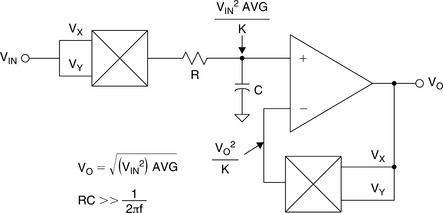

Figure 2-80 shows the circuit for computing the RMS value of a signal using the implicit method. Here, the output is fed back to the direct-divide input of a multiplier such as the AD734. In this circuit, the output of the multiplier varies linearly (instead of as the square) with the RMS value of the input. This considerably increases the dynamic range of the implicit circuit as compared to the explicit circuit. The disadvantage of this approach is that it generally has less bandwidth than the explicit computation.

While it is possible to construct such an RMS circuit from an AD734, it is far simpler to design a dedicated RMS circuit. The VIN2/VZ circuit may be current driven and need only be one quadrant if the input first passes through an absolute value circuit.
Figure 2-81 shows a simplified diagram of a typical monolithic RMS/DC converter, the AD536A. It is subdivided into four major sections: absolute value circuit (active rectifier), squarer/divider, current mirror, and buffer amplifier. The input voltage VIN, which can be AC or DC, is converted to a unipolar current, I1, by the absolute value circuit A1, A2. I1 drives one input of the one-quadrant squarer/divider which has the transfer function: I4 = I12/I3. The output current, I4, of the squarer/divider drives the current mirror through a lowpass filter formed by R1 and externally connected capacitor, CAV. If the R1CAV time constant is much greater than the longest period of the input signal, then I4 is effectively averaged. The current mirror returns a current, I3, which equals AVG[I4], back to the squarer/divider to complete the implicit RMS computation. Thus:

The current mirror also produces the output current, IOUT, which equals 2I4. IOUT can be used directly or converted to a voltage with R2 and buffered by A4 to provide a low impedance voltage output. The transfer function becomes:
The dB output is derived from the emitter of Q3, since the voltage at this point is proportional to −log VIN. Emitter follower, Q5, buffers and level shifts this voltage, so that the dB output voltage is zero when the externally supplied emitter current (IREF) to Q5 approximates I3. However, the gain of the dB circuit has a TC of approximately 3,300 ppm/°C and must be temperature compensated.
There are a number of commercially available RMS/DC converters in monolithic form which make use of these principles. The AD536A is a true RMS/DC converter with a bandwidth of approximately 450 kHz for VRMS > 100 mVRMS, and 2 MHz bandwidth for VRMS > 1 VRMS. The AD636 is designed to provide 1 MHz bandwidth for low level signals up to 200 mVRMS. The AD637 has a 600 kHz bandwidth for 100 mVRMS signals, and an 800 MHz bandwidth for 1 VRMS signals. Low cost, general-purpose RMS/DC converters such as the AD736 and AD737 (power-down option) are also available.
SECTION 2-13 Programmable Gain Amplifiers
Most systems with wide dynamic range need some method of adjusting the input signal level to the ADC. The ADC compares the input signal to a fixed voltage reference (+5 V or + 10 V are typical values). To achieve the rated precision of the converter, the maximum input should be fairly near its full-scale voltage. However, transducers have a wide range of output voltages. High gain is needed for a small sensor voltage, but with a large transducer output, a high gain will cause the amplifier or ADC to saturate. So some type of controllable gain device is needed. Such a device has a gain that is controlled by a DC voltage or, more commonly, a digital input. This device is known as a programmable gain amplifier (PGA, see Figure 2-82).

To understand the benefits of variable gain, assume an ideal PGA with two settings, gains of one and two. The dynamic range of the system is increased by 6 dB. Increasing the gain to four results in a 12 dB increase in dynamic range.
If the LSB of an ADC is equivalent to 10 mV of input voltage, the ADC cannot resolve smaller signals, but when the gain of the PGA is increased to two, input signals of 5 mV may be resolved. Thus, the processor can combine PGA gain information with the digital output of the ADC to increase its resolution by 1 bit. Essentially, this is the same as adding additional resolution to the ADC.
In practice, PGAs are not ideal, and their error sources must be studied. The most fundamental problem with PGA design is accurate gain programming. Electromechanical relays have minimal RON, but are otherwise unsuitable for gain switching. They are slow, large, and expensive. Silicon switches, as discussed in the section on switches and multiplexers (Chapter 7 of this book), have quite large RON, which is both voltage- and temperature-variable, and stray capacities, which may affect the AC parameters of a PGA using them.
To understand how RON can affect the performance of a PGA, let us consider a poor PGA design (Figure 2-83). An op amp is configured in the standard non-inverting gain circuit with four different gain-setting resistors, each grounded by a switch. Most silicon switches have ON resistance in the range of 100–500 Ω. Even if the ON resistance were as low as 25 Ω, the error for a gain of 16 would be 2.4%, much worse than 8 bits. Furthermore, RON drifts over temperature and varies from switch to switch. If the value of the feedback and gain-setting resistors were increased, noise and offset would become a problem. The only way to achieve accuracy with this circuit is to replace silicon switches with relays which have virtually no ON resistance.

It is better to use a circuit where RON is unimportant. In Figure 2-84, the switch is placed in series with the inverting input of an op amp. Since the input impedance of an op amp is very large, the RON of the switch is irrelevant. The gain is now determined by the external resistors. The RON may add a small offset error if the op amp bias current is significant.
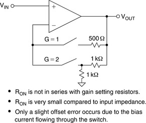
The AD526 amplifier uses this method of building a PGA and integrates it onto a single chip. The AD526 has five binary gain settings from 1 to 16, and its internal JFET switches are connected to the inverting input of the amplifier. The gain resistors are laser trimmed. The maximum gain error is only 0.02%, far better than the 2.4% error in Figure 2-85. The linearity is also very good at 0.001%. The AD526 is controlled by a latched digital interface.

This same design can be used to build the discrete PGA shown in Figure 2-86. It uses a single op amp, a quad switch, and precision resistors. The low noise AD797 replaces the JFET input op amp of the AD526, but almost any voltage feedback op amp could be used in this circuit. The ADG412 was picked for its low ON resistance of 35 Ω. The resistors were chosen to give gains of 1, 10, 100, and 1,000, but if other gains are required, the resistor values may easily be altered. Ideally, a trimmed resistor network should be used both for initial gain accuracy and for low drift over temperature. The 20 pF capacitor ensures stability and holds the output voltage when the gain is switched. The control signal to the switches turns one switch off a few nanoseconds before the second switch turns on. During this break, the op amp is open loop. If the capacitor was not used, the output would start slewing. Instead, the capacitor holds the output voltage during the switching. Since the time that both switches are open is very short, only 20 pF is needed. For slower switches, a larger capacitor may be necessary.
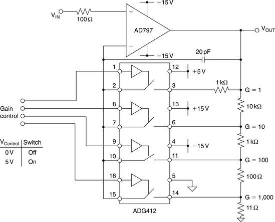
The PGA’s input voltage noise spectral density is only 1.65 nV/![]() at 1 kHz, only slightly higher than the noise performance of the AD797 alone. The increase is due to the noise of the ADG412, and the current noise of the AD797 flowing through the ON resistance. The noise was measured at a gain of 1,000 (worst case).
at 1 kHz, only slightly higher than the noise performance of the AD797 alone. The increase is due to the noise of the ADG412, and the current noise of the AD797 flowing through the ON resistance. The noise was measured at a gain of 1,000 (worst case).
The accuracy of the PGA is important in determining the overall accuracy of a system. The AD797 has a bias current of 0.9 μA, which, flowing in 35 Ω RON, results in an additional offset error of 31.5 μV. Combined with the AD797 offset, the total VOS becomes 71.5 μV (max). Offset temperature drift is affected by the change in bias current and ON resistance. Calculations show that the total temperature coefficient increases from 0.6 μV/°C to 1.6 μV/°C. These errors are small, and may not matter, but it is important to be aware of them. In practice, circuit accuracy and TC will be determined by the external resistors. Input characteristics such as CM range and input bias current are determined solely by the AD797. The circuit could be converted to single supply simply by changing the op amp. The switches do not need to be changed.
Another PGA configuration uses a DAC in the feedback loop of an op amp to adjust the gain under digital control (Figure 2-87). The digital code of the DAC controls its attenuation. Attenuating the feedback signal increases the closed-loop gain. A non-inverting PGA of this type requires a multiplying DAC with a voltage output (a multiplying DAC is a DAC with a wide reference voltage range which includes zero). For most applications of the PGA, the reference input must be capable of handling bipolar signals. The AD7846 is a 16-bit converter that meets these requirements. In this application, it is used in standard two-quadrant multiplying mode. The OP-213 is a low drift, low noise amplifier, but the choice of amplifier is flexible, and depends on the application. The input voltage range depends on the output swing of the AD7846, which is 3 V less than the positive supply and 4 V above the negative supply. A 1,000 pF capacitor is used in the feedback loop for stability.

The gain of the circuit is set by adjusting the digital inputs of the DAC, according to the equation given in Figure 2-87. D0–15 represents the decimal value of the digital code. For example, if all the bits were set high, the gain would be 65,536/65,535 = 1.000015. If the eight least significant bits are set high and the rest low, the gain would be 65,536/255 = 257.
Figure 2-88 shows the small signal response at a gain of 1 with a 100 mV square wave input. The bandwidth is a fairly high 4 MHz. However, this does reduce with gain, and for a gain of 256, the bandwidth is only 600 Hz. If the gain-bandwidth product were constant, the bandwidth in a gain of 256 should be 15.6 kHz; but the internal capacitance of the DAC reduces the bandwidth to 600 Hz.

The gain accuracy of the circuit is determined by the resolution of the DAC and the gain setting. At a gain of 1, all bits are on, and the accuracy is determined by the DNL specification of the DAC, which is ±1 LSB maximum. Thus, the gain accuracy is equivalent to 1 LSB in a 16-bit system, or 0.003%. However, as the gain is increased, fewer of the bits are on. For a gain of 256, only bit 8 is turned on. The gain accuracy is still dependent on the ± 1 LSB of DNL, but now that is compared to only the lowest 8 bits. Thus, the gain accuracy is reduced to 1 LSB in an 8-bit system, or 0.4%. If the gain is increased above 256, the gain accuracy is reduced further. The designer must determine an acceptable level of accuracy. In this particular circuit, the gain was limited to 256.
Non-inverting PGA circuits using an op amp are easily adaptable to single-supply operation, but the instrumentation amplifier topology does not lend itself to single-supply applications. However, the AMP-04 can be used with an external switch to produce the single-supply instrumentation PGA shown in Figure 2-89. This circuit has selectable gains of 1, 10, 100, and 500, which are controlled by an ADG511. The ADG511 was chosen as a single-supply switch with a low RON of 45 Ω. The gain of this circuit is dependent on the RON of the switches. Trimming is required at the higher gains to achieve accuracy. At a gain of 500, two switches are used in parallel, but their resistance causes a 10% gain error in the absence of adjustment.

Certain ΣΔ ADCs (e.g., AD7710, AD7711, AD7712, and AD7713) have built-in PGAs. Circuit design is much easier because an external PGA and its control logic are not needed. Furthermore, all the errors of the PGA are included in the specifications of the ADC, making error calculations simple. The PGA gain is controlled over the same serial interface as the ADC, and the gain setting is factored into the conversion, saving additional calculations to determine input voltage. This combination of ADC and PGA is very powerful and enables the realization of a highly accurate system, with a minimum of circuit design. The PGA function in this case is not a separate block requiring matching of resistors for accuracy in line with the expectation of the ΣΔ ADC. It is accomplished by modulating the duty cycle of the switched capacitors in the modulator, thus changing the gain (Figure 2-90).
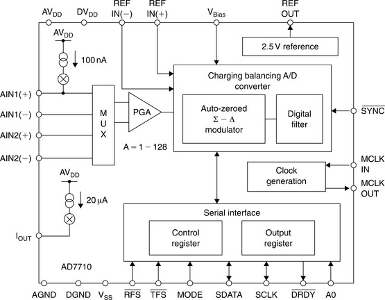
High speed VGAs are discussed in the RF/IF section (Section 4.6).
SECTION 2-14 Audio Amplifiers
Amplifiers
There are no specific audio specifications that apply to amplifiers. Obviously the amplifier needs to be of appropriate bandwidth and be low distortion. Several types have found application in the audio field. These include the AD797, OP275, and the AD711/12/13.
One application specific audio IC is the SSM2019 microphone preamplifier (see Figure 2-91). For use as a microphone preamplifier in high fidelity applications, a primary concern is that the circuit has to be low noise. The specification for the SSM2019 is 1 nV/![]() . The input to the SSM2019 is fully differential to interface with balanced microphones.
. The input to the SSM2019 is fully differential to interface with balanced microphones.

There is another application for microphone preamplifiers. Here the emphasis is on voice intelligibility rather than low noise. The target application is in communication systems and public address systems. The SSM2165/66/67 family is complete and flexible solutions for conditioning microphone inputs. The block diagram of the SSM2165 is shown in Figure 2-92. A low noise voltage controlled amplifier (VCA) provides a gain that is dynamically adjusted by a control loop to maintain a set compression characteristic. The compression ratio is set by a single resistor and can be varied from 1:1 to over 15:1 relative to the fixed rotation point. Signals above the rotation point are limited to prevent overload and to eliminate “popping.” A downward expander (noise gate) prevents amplification of noise or hum. This results in optimized signal levels prior to digitization, thereby eliminating the need for additional gain or attenuation in the digital domain that could add noise or impair accuracy of speech recognition algorithms (see also Figure 2-93).


Speaker driver power amplifiers are another application specific audio area. The main application challenge here is delivering enough audio power in a limited supply voltage environment such as is typically found in computers and games, while keeping the package power dissipation down to safe levels. As an example, the SSM2211 (Figure 2-94) is a high performance audio amplifier that delivers 1 WRMS of low distortion audio power into a bridge-connected 8 Ω speaker load (or 1.5 WRMS into 4 Ω load) (Figure 2-95). The SSM2211 is available in SO-8 and LFCSP (lead frame chip scale package) surface mount packages. The SO-8 features the patented Thermal Coastline lead frame. The Thermal Coastline package is further discussed in the power section.

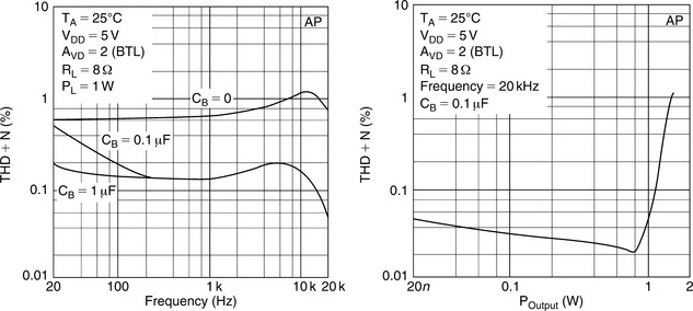
Voltage-Controlled Amplifiers
Audio signal levels are often controlled by using low distortion VCAs (voltage-controlled amplifiers) in the signal path. By using controlled rate of change drive to the VCAs, the “clicking” associated with switched resistive networks is eliminated. For example, the SSM2018T is a low noise, low distortion VCA applicable in high performance audio systems (Figures 2-96 and 2-97). The “T” suffix indicates a version that is factory trimmed for distortion and requires no subsequent user adjustments.

Despite the sonic advantages of using analog control of the signal level, it is sometimes useful to have the control voltage under digital control. In this case a DAC can be added to the VCA. An example of this configuration is the SSM2160 (Figure 2-98) which allows digital control of volume of six audio channels, with a master level control and individual channel controls. Low distortion VCAs are used in the signal path. Each channel is controlled by a dedicated 5-bit DAC providing 32 levels of gain. A master 7-bit DAC feeds every control port giving 128 levels of attenuation. Step sizes are nominally 1 dB and can be changed by external resistors. Channel balance is maintained over the entire master control range. Upon power-up, all outputs are automatically muted. A three-wire or four-wire serial data bus enables interfacing with most popular microcontrollers.

Line Drivers and Receivers
The function of sending/receiving audio signals between various system components has traditionally involved tradeoffs of one form or another. Fully differential or balanced transmission systems are best at rejecting low frequency and RF noise, so they are used for highest performance and are discussed in some detail in the following.
A typical audio system block diagram using differential or balanced transmission is shown in Figure 2-99. In concept, a balanced transmission system like this could use several input/output coupling schemes within the driver and receiver. Some major points distinguishing coupling method details are discussed briefly below, before addressing actual circuits.
A point worth noting is that the ± voltage drive to the line need not be exactly balanced to reap the benefits of balanced transmission. In fact the drive can be asymmetrical to some degree, and the signal will still be received at VOUT with correct amplitude and with good noise rejection. What does need to be provided is two well-balanced line-driving impedances, RO1 and RO2. Also, in conjunction with these balanced drive impedances, the associated (+) and (−) receiver input impedances should also be equal. The technical reasons for this will be apparent shortly.
Audio Line Receivers
An audio line receiver is simply a subtractor amplifier (Figure 2-100). From a DC and AC trim/balance perspective, the Figure 2-100 topology is most effective with resistors and amplifier made simultaneously in a single monolithic IC.

In applying circuits of the Figure 2-100 type (or other topologies which resistively load the source), a designer must bear in mind that all external resistances added to the four resistances can potentially degrade CMR, unless kept to proportional value increases. To place this in perspective, a 2.5 Ω or 0.01% mismatch can easily occur with wiring, and if not balanced out, this mismatch will degrade the CMR of otherwise perfectly matched 25 kΩ resistors to 86 dB. These circuits are therefore best fed from balanced, low impedance drive sources, preferably 25 Ω or less.
The SSM2141 and SSM2143 are monolithic IC line receivers which work very much like the circuit of Figure 2-100 differing only in their individual gains. The SSM2141 operates as a unity-gain device, while the SSM2143 operates either at a nominal gain of 0.5 (–6 dB), or it can optionally be strapped with the input/output of the resistor pairs reversed, to operate at a gain of 2 (6 dB).
Both devices operate from supplies up to ± 18 V, can drive 600 Ω loads, and have low distortion and excellent CMR characteristics. For reference, the op amp used in these receivers is similar to one-half of an OP271. The output appears at pin 6 and is uncommitted; with conventional use it gets tied to R4 (pin 5) for feedback. However, if desired, an external in-loop buffer can optionally be added. This step will allow either line receiver device to drive even lower Z loads if desired.
Perhaps the most outstanding attribute of these devices is their CMR performance, shown in Figure 2-101(A) (these data are for the SSM2141, but for the SSM2143 they are similar). For the SSM2141 the DC to 1 kHz CMR is typically 100 dB, and even at 10 kHz it is still about 80 dB. The SSM2143 (not shown), using lower resistor values, has a somewhat lower typical CMR of 90 dB, but maintains this to about 10 kHz.
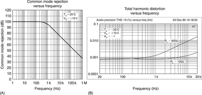
The SSM2141 THD + N performance also shown in Figure 2-101(B) is also very good for both 600 Ω and 100 kΩ loads.
With a companion differential line driver (next section), these two line receivers allow convenient as well as flexible interfacing between points in audio systems, as well as other instrumentation up to 100 kHz. However, they both are also more generally useful as flexible gain blocks within a system, not necessarily requiring the full CM performance aspects. For example, they are useful as either precise inverting or non-inverting gains blocks, due to the very accurate internal resistor ratios. With the SSM2141 typical gain accuracy of 0.001%, very precise, single chip unity-gain inverters and summers can be built at low overall cost.
Audio Line Drivers
Unlike the case for the differential line receiver, a standard circuit topology for differential line drivers is not quite as clear-cut. Two circuit types are discussed in this section, with their contrasts in performance and complexity.
On the other hand, the inherent features of laser-trimmed monolithic technology can make a complex circuit such as the balanced line driver thoroughly practical. Like the SSM2141 and SSM2143 line receivers, applying these concepts to a driver circuit results in an efficient and useful IC. This product, the SSM2142 balanced line driver, is shown in functional form in Figure 2-102.

The SSM2142 is designed for a single ended to differential gain of 2 times, and in use can be simply strapped with the respective FORCE/SENSE pins tied together. In a system application, the SSM2142 is used with either an SSM2143 or an SSM2141 line receiver, with the differential-mode signal being transmitted via shielded twisted pair cable. This hookup comprises a complete single ended to differential and back to single-ended transmission system, with noise isolation in the process.
With the use of the SSM2143 gain of 0.5, the SSM2142 gain of 2 is complemented, and the overall system gain is unity (Figure 2-103). If the SSM2141 is used as the receiver, the gain is 2 overall, implying the use of a terminating resistor at the receiver. The THD + N performance of the unity-gain SSM2142/SSM2143 system is shown in Figure 2-104, for the conditions of a 5 VRMS input/output signal, both with/without a 500′ cable.
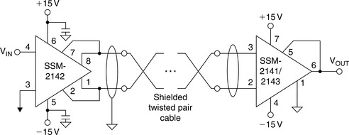
As should be obvious, these drivers do not offer galvanic isolation, which means that in all applications there must be a DC current path between the grounds of the driver and the final receiver. In practice, however, this is not necessarily a problem.
Class D Audio Power Amplifiers
Theory of Operation
A Class D audio amplifier is basically a switch-mode or PWM amplifier and is one of a number of different classes of amplifiers. Following is a look at the definitions for the main classifications:
Class A—In a Class A amplifier, the output device(s) are continuously conducting for the entire cycle, or in other words there is always bias current flowing in the output devices. This topology has the least distortion and is the most linear, but at the same time is the least efficient, at around 20%. Therefore, the quiescent dissipation is high. In fact the dissipation is constant, regardless of how much power is delivered to the load. A Class A amplifier output is typically not complementary, with a high and low side output device(s).
Class B—In a Class B amplifier the output device(s) only conduct for half the sinusoidal cycle (one conducts for the positive half cycle, and one conducts for the negative half cycle). If there is no signal, then there is no current flow in the output devices. This class of amplifier is obviously more efficient than Class A, at about 50%, but has some distortion at the crossover point due to the time it takes to turn one device off and turn the other device on. This is referred to as crossover notch distortion. Since it occurs at the point of minimum signal (the zero crossing), its effect is very obvious.
Class AB—This type of amplifier is a combination of the above two types, and is probably the most common type of power amplifier in existence. Here both devices are allowed to conduct at the same time, but just by a small amount near the crossover point. Hence each device is conducting for more than half a cycle but less than the whole cycle, so the inherent nonlinearity (crossover distortion) of Class B designs is overcome, without the inefficiencies of a Class A design. Efficiencies for Class AB amplifiers can also be about 50%. There are variations of Class AB, depending on how much of the cycle both of the output devices conduct. Obviously, the more they both conduct, the lower the efficiency, but also the higher the linearity (Figure 2-105).

Class D—This class of amplifier is a switching amplifier as mentioned above. In this type of amplifier, the switches are either fully on or fully off, significantly reducing the power losses in the output devices. This is very similar to the difference between linear power regulators and switch-mode regulators.
Efficiencies of 90–95% are possible. Audio Class D amplifiers use a modulator to convert the input audio signal into a switching waveform used to control the output switches. PWM is the most commonly used modulation scheme. In PWM, the audio signal is used to modulate a PWM carrier signal which drives the output devices. The output devices then drive a lowpass filter to remove the high frequency PWM carrier frequency, while retaining the desired audio content. The speaker is one of the elements in this filter, and is situated at the filter output.
Class D amplifiers take on many different forms; some can have digital inputs and some can have analog inputs.
However, audio quality in PWM amplifiers can be limited: THD is typically 0.1% or worse, and PSRR is poor (see Reference 1). PSRR can be improved by sensing power supply variations and adjusting the modulator’s behavior to compensate, as proposed in Reference 1. However, this alone will not suppress the THD produced by inherent PWM nonlinearity or power stage nonlinearity.
These THD and power supply noises can both be suppressed with feedback from the power stage outputs (see Reference 2), which incorporates the feedback around an analog PWM modulator.
PWM is attractive because it allows >100 dB audio-band SNR at low clock rates near 400 kHz, limiting switching losses. Also, many PWM modulators are stable to near 100% modulation, allowing high output power before overloading. However, PWM has several problems. First, the PWM process inherently adds distortion in many modulation schemes (see Reference 3) and second, harmonics of the PWM switching frequency produce EMI in the AM band.
ΣΔ modulation does not share these problems, but nonetheless has not traditionally been used for Class D (see Reference 3), because conventional 1-bit ΣΔ modulators are only stable to 50% modulation, and power efficiency is limited because typical output data rates are > 1 MHz, when ≥64× oversampling rate is needed to achieve sufficient audio-band SNR. However, Analog Devices has enhanced the traditional 1-bit ΣΔ architecture to overcome these problems, and created ΣΔ-based Class D amplifier chips which have performance advantages over competitor PWM-based products.
Device Architecture
The AD1990/2/4/6 family of chips are two-channel bridge tied load (BTL) switching audio power amplifiers with integrated ΣΔ modulator. Hereafter, “AD199x” will be used to refer to this product family.
The AD199x modulator accepts a low power analog input signal (of 5 Vp−p maximum amplitude), and generates a switching waveform to drive speakers directly. One of the two modulators can control both output stages thereby providing twice the current for single-channel applications. A digital, microcontroller-compatible interface provides control of reset, mute, and PGA gain as well as output signals for thermal and over-current error conditions. The output stage can operate from supply voltages ranging from 8 V to 20 V. The analog modulator and digital logic operate from a 5 V supply.
The power stage of the AD199x is arranged internally as four transistor pairs, which are used as two H-bridge outputs to provide stereo amplification. The transistor pairs are driven by the output of the ΣΔ modulator. A user selectable non-overlap time is provided between the switching of the high side transistor and low side transistor to ensure that both transistors are never on at the same time. The AD199x implements turn-on pop suppression to eliminate any pops or clicks following a reset or un-mute.
Analog Input Section
The analog input section uses an internal amplifier to bias the input signal to the reference level. A DC blocking capacitor should be connected to remove any external DC bias contained in the input signal.
The Sigma–Delta Modulator
The modulator uses a 1-bit, seventh-order feedforward architecture. The quantizer output drives the switching power stage, whose pulses are fed back to a continuous-time (CT) first integrator. This allows fullest possible integration of the pulse waveform, maximizing error correction. If the first integrator were discrete-time (DT), its sampling process would often miss important information about errors in pulse edge timing and shape, which would reduce the error-correcting effectiveness of the feedback loop.
The CT integrator bandwidth of 100 kHz gives anti-alias filtering for the subsequent DT, switched-capacitor (SC) integrators. The SC integrators and quantizer are clocked at 6 MHz, corresponding to 128× oversampling.
For the modulator, seventh order is more than enough to achieve 100 dB SNR with traditional aggressive noise shaping (see Reference 5). However, this gives instability for modulation >50%, limiting the maximum output power with stable operation to just 25% of theoretical full power. To overcome this limitation, we use less aggressive noise shaping to maintain stability to 90% modulation. This gives good sound quality at higher power, but requires high modulator order to get acceptable SNR.
Fortunately, all integrators after the first can be SC. The high first integrator gain relaxes noise requirements for the SC ones, allowing small sampling caps (50 fF), and low power single-stage op amps. Resonator feedbacks to integrators 2, 4, and 6 reduce low frequency noise, by placing NTF zeroes at 12 kHz, 22 kHz, and 40 kHz. When PVDD = 12 V, integrated audio-band quantization noise is 25 μVRMS and additional thermal noise yields total integrated audio noise of 50 μVRMS. Maximum output is 7.8 VRMS, giving 104 dB dynamic range.
The modulator described to this point would become unstable for large inputs > 90% full-scale. Output transients resulting from the instability would bear little relationship to the desired signal, and would sound bad. To solve this problem, the modulator input is monitored, and when large signals that could cause instability are detected, integrators 3–7 of the modulator are reset. This effectively converts the modulator to a second order, unconditionally stable configuration. The loop gain is reduced relative to the “normal” seventh-order configuration, so that noise shaping is less effective and more quantization noise reaches the output. However, this elevated noise is superimposed on a large output signal that is now closer to the desired waveform, and the composite sound is better than when the modulator is allowed to become unstable.
Driving the H-Bridge
Each channel of the switching amplifier is controlled by a four-transistor H-bridge to give a differential output stage. The outputs of the H-bridges, OUTR+, OUTR−, OUTL+, and OUTL− will switch between PVDD and PGND as determined by the sigma delta (ΣΔ) modulator. The power supply that is used to drive the power stage of the AD199x should be in the range of + 8 V to + 20 V and be capable of supplying enough current to drive the load. This power supply is connected across the PVDD and PGND pins. The feedback pins, NFR+, NFR−, NFL+, and NFL− are used to supply negative feedback to the modulator. The pins are connected to the outputs of the H-bridge using a resistor divider network as shown in Figure 2-106.

External Schottky diodes can be used to reduce power loss during the non-overlap time when neither of the high side or low side transistors is on. During this time neither transistor is driving the OUTx pin. The purpose of the inductors is to keep current flowing.
For example, the OUTx pin may approach and pass the PGND level to achieve this. When the voltage at the OUTx pin is 0.7 V below PGND, the parasitic diode associated with the low side transistor will become forward biased and turn on. When the high side transistor turns on, the voltage at OUTx will rise to PVDD and will reverse bias the parasitic diode. However, by its nature the parasitic diode has a long reverse recovery time and current will continue to flow through it to PGND thus causing the entire circuit to draw more current than necessary. The addition of the Schottky diodes prevents this from happening. When the OUTx pin goes more than 0.3 V below PGND the Schottky diode becomes forward biased. When the high side transistor turns on, the Schottky diode becomes reverse biased. The reverse recovery time of the Schottky diode is significantly faster than the parasitic diode so far less current is wasted. A similar effect happens when the inductor induces a current which drives the OUTx pin above PVDD. Figure 2-106 shows how the external components of a system are connected to the pins of the AD199x to form the H-bridge configuration.
Amplifier Gain
Selecting the Modulator Gain
The AD199x modulator can be thought of as a switching analog amplifier with a voltage gain controlled by two external resistors forming a resistor divider between the OUTxx pins and PGND. The center of the resistor divider is connected to the appropriate feedback pin NFx. Selecting the gain along with the PVDD voltage will determine how much power can be delivered to a load for a fixed input signal. The gain of the modulator is controlled by the values of R1 and R2 (see Figure 2-107) according to the equation:
 (2-23)
If the voltage at the NFx pins exceeds 5 V, ESD protection circuitry will turn on, to protect low voltage circuitry inside the chip that is connected to NFx. When the protection circuit is active, it introduces nonlinear behavior into the modulator feedback loop, which degrades audio quality. To avoid this, R1, R2, and the gain should be selected in a manner that limits max voltage at NFx to <5 V. For optimal modulator stability and audio quality, use the formula:
 (2-24)
The ratio of the resistances sets the gain rather than the absolute values. However, the dividers provide a path from the high voltage supply to ground, so the values should be large enough to produce negligible loss due to quiescent current.
The chip contains a calibration circuit to minimize voltage offsets at the speaker, which helps to minimize clicks and pops when muting or un-muting. Optimal performance is achieved for the offset calibration circuit when the feedback divider resistors sum to 6 kΩ (meaning that (R1 + R2) = 61 kΩ).
Power-Up Considerations
Careful power-up of the AD199x is necessary to ensure correct operation and avoid possible latch-up issues. The AD199x should be powered up with RST/PDN and MUTE held low until all the power supplies have stabilized. Once the supplies have stabilized, the AD199x can be brought out of reset by bringing RST/PDN high and then MUTE can be brought high as required.
On/Off/Mute Pop Noise Suppression
The AD199x features pop suppression which is activated when the part is reset or taken out of mute. The pop suppression is achieved by pulsing the power outputs to bring the outputs of the LC filter from 0 V to mid-scale in a controlled fashion. This feature eliminates unwanted transients on both the outputs and the high voltage power supply.
Thermal Protection
The AD199x features thermal protection. When the die temperature exceeds approximately 135°C, the thermal warning error output (ERR1) is asserted. If the die temperature exceeds approximately 150°C, the thermal shutdown error output (ERR2) is asserted. If this occurs, the part shuts down to prevent damage. When the die temperature drops below approximately 120°C, both error outputs are negated and the part returns to normal operation.
Over-Current Protection
The AD199x features over-current or short-circuit protection. If the current through any power transistors exceeds 4A, the part goes into mute and the over-current error output (ERR0) is asserted. This is a latched error and does not clear automatically. To clear the error condition and restore normal operation, the part must be either reset, or MUTE must be asserted and negated.
Good board layout and decoupling are vital for correct operation of the AD199x. Due to the fact that the part switches high currents, there is the potential for large PVDD bounce each time a transistor switches. This can cause unpredictable operation of the part. To avoid this potential problem, close chip decoupling is essential. It is also recommended that the decoupling capacitors are placed on the same side of the board as the AD199x, and connected directly to the PVDD and PGND pins. By placing the decoupling capacitors on the other side of the board and decoupling through vias, the effectiveness of the decoupling is reduced.
This is because vias have inductive properties and therefore prevent very fast discharge of the decoupling capacitors. Best operation is achieved with at least one decoupling capacitor on each side of the AD199x, or (optionally) two capacitors per side can be used to further reduce the series resistance of the capacitor. If these decoupling recommendations cannot be followed and decoupling through vias is the only option, the vias should be made as large as possible to increase surface area, thereby reducing inductance and resistance (Figure 2-108).
Application Considerations
Audio Fidelity and EMI Reduction
The AD199x amplifiers deliver audiophile sound quality (THD < 0.003%; SNR > 103 dB; PSRR > 65 dB) with 50% lower heat dissipation than traditional linear amplifiers. The THD performance is 40 dB better than typical “open-loop” competitors and 10–20 dB better than most closed-loop ones. This breakthrough performance is achieved through Analog Devices’ closed-loop, mixed-signal integration of seventh-order Sigma–Delta (ΣΔ) modulator technology with high power output drive circuitry and bridge circuitry. Radiated and conducted out-of-band RF emissions are minimized with Analog Devices’ advanced modulation techniques and closed-loop, Sigma–Delta (ΣΔ) architecture to enable a significant reduction in EMI.
Power levels range from Stereo 5 W (Mono 10 W) to Stereo 40 W (Mono 80 W). The AD1994 can be configured in a modulator-only mode. This, coupled with external high power FETs, enables very high power amplification, limited only by the power stage design. The parts also incorporate critical peripheral functions, including pop/click suppression circuitry as well as short-circuit, overload, and temperature protection.
THD + N for 1 kHz Sinewave
Figures 2-109 and 2-110 show FFTs measured with signals of 1 kHz at 1 μW and 1 W output power levels. The 1 μW FFT (Figure 2-109) demonstrates that the noise floor is tonefree for low power inputs.


The 1 W power level in Figure 2-110 is intended to represent a realistic listening level. Harmonic distortion is evident, but the 0.00121% THD is an unprecedented level for this signal condition in a single chip Class D amplifier.
Figure 2-111 shows how THD varies with frequency, when the signal condition is a sinewave of 1 W output power.

Higher modulator loop gain at low frequencies enables better correction of modulator and power stage errors, giving better THD than at higher frequencies. THD is actually 0.001% (–100 dB) or better up to hundreds of Hz. The apparent THD improvement at audio frequencies above 6 kHz is a misleading artifact of the measurement setup, which was unable to detect harmonics beyond its 20 kHz bandwidth. For 20 kHz fundamentals, actual THD is near 0.01% (–80 dB), at ultrasonic, inaudible frequencies.
THD + N Versus Output Power, 1 kHz Sine
Figure 2-112 shows how THD + N varies with output power, for 1 kHz sinewaves. There are two curves in the plot. The first (o) is for a low power application where PVDD = 12 V and the load is 6 Ω (the default measurement setup). The second (x) is for a higher power application where PVDD = 20 V and the load is 4 Ω.

In these curves, there are three distinct regions of performance. The first is at the lowest output power levels, where the modulator is seventh order, and THD + N is best. The second performance region is at significant output power, when the modulator order is lowered from seventh to second to prevent instability.
The second-order configuration only allows 65 dB THD + N, because quantization noise is now elevated due to the lower modulator order. However, this higher noise is difficult to hear above the loud, energetic output. The third performance region is at highest output powers, where clipping occurs, and distortion associated with clipping causes THD to degrade rapidly.
IMD
Figure 2-113 shows the intermodulation distortion (IMD) resulting from a 1 W, 19 kHz, and 20 kHz twin-tone stimulus. The 1 kHz second-order product is approximately 98 dB below the tones.

Crosstalk
Crosstalk between channels is a concern in chips with multiple audio channels. To investigate crosstalk, we drove one channel of the chip with a 1 kHz, 1 W (+7.8 dBV) sinewave, while leaving the other channel idle (0 input). We then measured the idle channel: results are shown in Figure 2-114. The −89 dBV 1 kHz tone in the idle channel is 97 dB below the driven channel’s signal.

Power Efficiency
Figure 2-115 shows power efficiency up to 5 W output power. The 50 mW/channel modulator power consumption and power stage consumption are both included in this calculation. (If we included only the power stage consumption but excluded the modulator, as is sometimes done, the efficiency number would improve.)

SECTION 2-15 Auto-Zero Amplifiers
Chopper Amplifiers
Chopper type amplifier topologies have existed for decades. Initial chopper designs actually involved switching the AC coupled input signal and synchronous demodulation of the AC signal to re-establish the DC signal (see Figure 2-116). While these amplifiers achieved very low offset, low offset drift, and very high gain, they had limited bandwidth (it is a sampled system after all) and required filtering to remove the large ripple voltages generated by the chopping action. In the earliest implementations the chopping switches were actually relays, commonly switching on the order of 400 Hz.

Virtually all modern IC chopper amplifiers actually use an auto-zero approach utilizing a two (or more) stage composite amplifier structure similar to the chopper-stabilized scheme (see Figure 2-117). One stage provides nulling action, while the other provides wideband response. Together, the two stages provide very high voltage gain as they are connected in series.

Chopper-stabilized amplifiers solved the bandwidth limitations of the classic implementation by combining the chopper amplifier (used as a stabilizing amplifier) with a conventional wideband amplifier that remained in the signal path. Since the main signal path is not sampled, the bandwidth of the system is determined by the bandwidth of the signal amplifier. It can exceed the chopping frequency.
These chopper-stabilized designs are capable of inverting operation only since the stabilizing amplifier is connected to the non-inverting input of the wideband amplifier.
In this approach, the inputs of the nulling stage are shorted together during the first phase of the operational cycle. During this nulling phase, amplified feedback is used to virtually eliminate the offset of the nulling stage. The feedback voltage is impressed on a storage capacitor so that during the second, or “output,” phase the offset remains nulled while the inputs are now connected to the signal of interest.
In the output phase, the nulled input stage and the wideband stage in series amplify the signal. The output of the nulled stage is impressed on a storage capacitor so that when the cycle returns to the nulling phase (inputs shorted together), the output continues to reflect the last input voltage value. Higher frequency signals bypass the nulling stage through feedforward techniques, making wide bandwidth operation possible.
While this technique provides DC accuracy and better frequency response, along with the flexibility of inverting and non-inverting configurations, it is prone to high levels of digital switching noise that may limit the usefulness of the wider bandwidth.
Auto-Zero Amplifiers Improve on Choppers
ADI’s auto-zero amplifiers use a similar architecture with some major improvements. Dual nulling loops, special switching logic, and innovative compensation techniques result in dynamic performance improvements while minimizing total die area. The result: amplifiers retain the high gain and DC precision of the auto-zero approach while minimizing the negative effects of digital switching on the analog signal—at half the cost. Typical offset voltage is under 1 μV and the offset drift is less than 10 nV/°C. Voltage gain is more than 10 million, while PSRR and CMRR are well above 120 dB. Input voltage noise is only 1 μVp−p from DC to 10 Hz.
Many auto-zero amplifiers are plagued by long overload recovery times due to the complicated settling behavior of the internal nulling loops after saturation of the outputs. Analog Devices’ auto-zero amplifiers have been designed so that internal settling occurs within one or two clock cycles after output saturation occurs. The result is that the overload recovery time is more than an order of magnitude shorter than previous designs and is comparable to conventional amplifiers.
The careful design and layout of the AD855x amplifiers reduce digital clock noise and aliasing effects by as much as 40 dB versus older designs.
In many cases the bandwidth required by the applications is such that the small amount of digital feedthrough can be eliminated by filtering. Output filtering is also useful in limiting the broadband noise of the signal amplifier.
The AD857x reduces the effects of digital switching on the analog signal by using a patented digital spread-spectrum technique. As can be seen from Figures 2-118 and 2-119, the AD857x virtually eliminates the energy spike seen in other auto-zero amplifiers at the switching frequency. It also reduces aliasing products between the chopping clock and the input signal to the noise floor. The only penalty for this breakthrough performance is a slight increase in voltage noise from the industry-best 1 μVp−p from DC to 10 Hz of the AD855x design.

Implementation
The actual circuit implementation of an IC auto-zero amplifier is much more complicated than the simplified version described above. Multiple nulling loops are combined with innovative compensation, and signal paths are fully differential. Internal voltages are controlled carefully to prevent saturation of the nulling circuitry. In addition, special logic designs are utilized, and careful layout is required to minimize parasitic effects. These techniques result in stable, reliable operation and minimize unwanted digital interaction with the analog signals.
The frequency response of the nulling and wideband amplifiers is carefully tailored so that low frequency errors (DC circuit offsets and low frequency noise) are nulled while high frequency signals are amplified as in a conventional op amp. This nulling of low frequency errors has an important consequence for voltage noise. The very low frequency 1/f noise behavior seen in conventional amplifiers is not present in auto-zero amplifiers. For applications with long measurement times on slowly varying signals, the noise performance is better than the best low noise conventional amplifier designs (Figure 2-120).
Figure 2-120: Noise comparison between conventional precision amplifiers and chopper-stabilized op amps
In this IC implementation, the size of the on-chip storage capacitors is limited to achieve a cost-effective die size. The small storage capacitors require careful attention to the switch design and layout so that charge injection effects do not create large offset errors. Switch leakage must also be minimized to maintain circuit accuracy, especially at high temperatures. In the AD855x and AD857x amplifiers, the switches have been optimized for accurate operation up to + 125°C.
Operation Description
The simplified circuit consists of the nulling amplifier (AA), the wideband amplifier (AB), storage capacitors (CM1 and CM2), and switches for the inputs and storage capacitors. There are two phases (A and B) per clock cycle.
In Phase A, the auto-zero phase (Figure 2-121), the nulling amplifier auto-zeros itself while the wideband amplifier amplifies the input signal directly. The inputs of the nulling amp are shorted together and to the inverting input terminal (CM input voltage). The nulling amplifier nulls its inherent offset voltage through its nulling terminal gain (–BA). The nulling voltage is also impressed on CM1. The signal at the input terminals is amplified directly by the wideband amplifier.
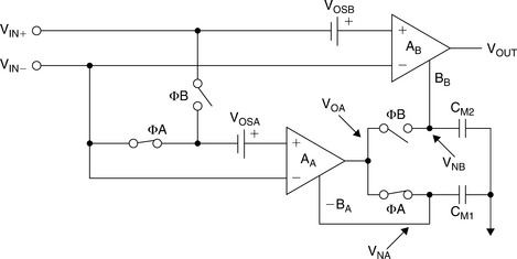
In Phase B, the output phase (Figure 2-122), both amplifiers amplify the input signal. The inputs of the nulling amplifier are connected to the input terminals. The nulling voltage of the nulling amplifier is now stored on capacitor CM1 and continues to minimize its output offset voltage. The instantaneous input signal is amplified by the nulling amplifier into the wideband amplifier through the wideband amplifier nulling terminal gain (BB). The output voltage of the nulling amplifier is also impressed on storage capacitor CM2. The total amplifier gain is approximately equal to the product of the nulling amplifier gain and the wideband amplifier gain. The total offset voltage is approximately equal to the sum of the nulling amplifier and wideband amplifier offset voltages divided by the gain of the wideband amplifier nulling terminal. By making this gain very large, the total amplifier effective offset voltage becomes very small.

Both VOSA and VOSB are highpass filtered “corner frequency” of highpass filter set by chopping frequency.
As the cycle returns to the nulling phase, the stored voltage on CM2 continues to effectively correct the DC offset of the composite amplifier. The cycle from nulling to output phase is repeated continuously at a rate set by the internal clock and logic circuits. This model circuit, while simplified from the actual design, accurately depicts the essentials of the auto-zero technique.
A more rigorous analysis is available in the data sheets for the AD855X.
References: Auto-Zero Amplifiers
1 Sheingold D.H., ed. Transducer Interfacing Handbook. Boston, MA: Analog Devices, Inc., 1981.
2 Kitchin C., Counts L. Instrumentation Amplifier Applications Guide. Boston, MA: Analog, Devices, Inc., 1991.
3 Amplifier Applications Guide. Boston, MA: Analog Devices, Inc.; 2002.
4 System Applications Guide. Boston, MA: Analog Devices, Inc.; 1993.
5 J. Sylvan, “High-speed comparators provide many useful circuit functions when used correctly.” Ask The Applications Engineer—5.
6 Moghimi R. Curing Comparator Instability with Hysteresis. Analog Dialogue. Vol. 34(7), 2000.
7 Erdi G. A 300 V/µs Monolithic Voltage Follower. IEEE Journal of Solid State Circuits. 1979;Vol. SC-14(6):1059–1065. December
8 R.A. Gosser, “Wideband Transconductance Generator,” US Patent 5,150,074, filed, May 3, 1991, issued September 22, 1992.
9 D.F. Bowers, “A 6.8 mA Closed-Loop Monolithic Buffer with 120 MHz Bandwidth, 4000 V/µs Slew Rate, and ± 12 V Signal Compatibility,” 1994 Bipolar/BiCMOS Circuits and Technology Meeting 1.3, pp. 23–26.
10 B. Gilbert, ISSCC Digest of Technical Papers 1968, February 16, 1968, pp. 114–115.
11 Gilbert B. Journal of Solid State Circuits. 1968;Vol. SC-3:353–372. December
12 Ruthroff C.L. Some Broadband Transformers. Proc. I.R.E. 1959;Vol. 47:1337–1342. August
13 J.M. Bryant, Mixers for High Performance Radio, Wescon 1981: Session 24 (Published by Electronic Conventions, Inc., Sepulveda Blvd., El Segundo, CA).
14 P.E. Chadwick, High Performance IC Mixers. IERE Conference on Radio Receivers and Associated Systems, Leeds, 1981, IERE Conference Publication No. 50.
15 P.E. Chadwick, Phase Noise, Intermodulation, and Dynamic Range. RF Expo, Anaheim, CA, January, 1986.
16 Daniel H., Sheingold R. Nonlinear Circuits Handbook, 3rd Edition, Inc.: Analog Devices, 1974.
17 Hughes R.S. Logarithmic Amplifiers. Dedham, MA.: Artech House, Inc., 1986.
18 Barber W.L., Brown E.R. A True Logarithmic Amplifier for Radar IF Applications. IEEE Journal of Solid State Circuits. 1980;Vol. SC-15(3):291–295. June
19 Broadband Amplifier Applications. September: Plessey Co. Publication P.S. 1938; 1984.
20 Gay M.S. SL521 Application Note. Norwood, Ma: Plessey Co., 1966.
21 Amplifier Applications Guide. Boston, MA: Analog Devices, Inc.; 1992. Section 9.
22 Kitchen C., Counts L. RMS-to-DC Conversion Application Guide, Second Edition. New York: Analog Devices, Inc., 1986.
23 B. Gilbert, A Low Noise Wideband Variable-Gain Amplifier Using an Interpolated Ladder Attenuator. IEEE ISSCC Technical Digest, 1991, pp. 280, 281, 330.
24 B. Gilbert, “A Monolithic Microsystem for Analog Synthesis of Trigonometric Functions and their Inverses,” IEEE Journal of Solid State Circuits, Vol. SC-17, No. 6, December
25 L. Zhang, et al., “Real-time Power Supply Compensation for Noise-shaped Class D Amplifier,” Presented at 117th AES Convention, San Francisco CA, USA, October 28–31, 2004.
26 Berkhout M. Integrated 200-W class-D audio amplifier. Journal of Solid State Circuits. 2003;Vol. 38:1198–1206. July
27 K. Nielsen, “A review and comparison of pulse width modulation (PWM) methods for analog and digital input switching power amplifiers,” Presented at 102nd AES Convention, Munich, Germany, March 22–25, 1997.
28 Morrow P., et al. A 20 Watt Stereo Class-D Audio Output Power Stage in 0.6 µm BCDMOS Technology. Journal of Solid State Circuits. Vol. 39, 2004. November.
29 Norsworthy S.R., Schreier R., Temes G.C., eds.. Delta-Sigma Data Converters. IEEE press; 1997:153–155.
30 E. Gaalaas, B. Y. Liu, N. Nishimura, R. Adams, K. Sweetland, and R. Morajkar, “Integrated Stereo ΣΔ Class D Amplifier,” Presented at the 118th Convention, Barcelona, Spain, May 28–31, 2005.
31 Gaalaas E., Liu B.Y., Nishimura N., Adams R., Sweetland K. Integrated Stereo ΣΔ Class D Amplifier. IEEE Journal of Solid-State Circuits. 2005;Vol. 40(12):2388–2397.