
The Controller Area Network (CAN) is a serial bus communications protocol developed by Bosch (an electrical equipment manufacturer in Germany) in the early 1980s. Thereafter, CAN was standardized as ISO-11898 and ISO-11519, establishing itself as the standard protocol for in-vehicle networking in the auto industry. In the early days of the automotive industry, localized stand-alone controllers had been used to manage various actuators and electromechanical subsystems. By networking the electronics in vehicles with CAN, however, they could be controlled from a central point, the engine control unit (ECU), thus increasing functionality, adding modularity, and making diagnostic processes more efficient.
Early CAN development was mainly supported by the vehicle industry, as it was used in passenger cars, boats, trucks, and other types of vehicles. Today the CAN protocol is used in many other fields in applications that call for networked embedded control, including industrial automation, medical applications, building automation, weaving machines, and production machinery. CAN offers an efficient communication protocol between sensors, actuators, controllers, and other nodes in real-time applications, and is known for its simplicity, reliability, and high performance.
The CAN protocol is based on a bus topology, and only two wires are needed for communication over a CAN bus. The bus has a multimaster structure where each device on the bus can send or receive data. Only one device can send data at any time while all the others listen. If two or more devices attempt to send data at the same time, the one with the highest priority is allowed to send its data while the others return to receive mode.
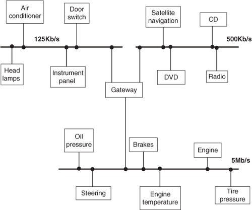
As shown in Figure 9.1, in a typical vehicle application there is usually more than one CAN bus, and they operate at different speeds. Slower devices, such as door control, climate control, and driver information modules, can be connected to a slow speed bus. Devices that require faster response, such as the ABS antilock braking system, the transmission control module, and the electronic throttle module, are connected to a faster CAN bus.
The automotive industry’s use of CAN has caused mass production of CAN controllers. Current estimate is that 400 million CAN modules are sold every year, and CAN controllers are integrated on many microcontrollers, including PIC microcontrollers, and are available at low cost.
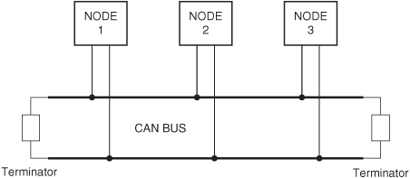
Figure 9.2 shows a CAN bus with three nodes. The CAN protocol is based on CSMA/ CD+AMP (Carrier-Sense Multiple Access/Collision Detection with Arbitration on Message Priority) protocol, which is similar to the protocol used in Ethernet LAN. When Ethernet detects a collision, the sending nodes simply stop transmitting and wait a random amount of time before trying to send again. CAN protocol, however, solves the collision problem using the principle of arbitration, where only the higheest priority node is given the right to send its data.
There are basically two types of CAN protocols: 2.0A and 2.0B. CAN 2.0A is the earlier standard with 11 bits of identifier, while CAN 2.0B is the new extended standard with 29 bits of identifier. 2.0B controllers are completely backward-compatible with 2.0A controllers and can receive and transmit messages in either format.
There are two types of 2.0A controllers. The first is capable of sending and receiving 2.0A messages only, and reception of a 2.0B message will flag an error. The second type of 2.0A controller (known as 2.0B passive) sends and receives 2.0A messages but will also acknowledge receipt of 2.0B messages and then ignore them.
Some of the CAN protocol features are:
CAN bus is multimaster. When the bus is free, any device attached to the bus can start sending a message.
CAN bus protocol is flexible. The devices connected to the bus have no addresses, which means messages are not transmitted from one node to another based on addresses. Instead, all nodes in the system receive every message transmitted on the bus, and it is up to each node to decide whether the received message should be kept or discarded. A single message can be destined for a particular node or for many nodes, depending on how the system is designed. Another advantage of having no addresses is that when a device is added to or removed from the bus, no configuration data needs to be changed (i.e., the bus is “hot pluggable”).
CAN bus offers remote transmit request (RTR), which means that one node on the bus is able to request information from the other nodes. Thus instead of waiting for a node to continuously send information, a request for information can be sent to the node. For example, in a vehicle, where the engine temperature is an important parameter, the system can be designed so the temperature is sent periodically over the bus. However, a more elegant solution is to request the temperature as needed, since it minimizes the bus traffic while maintaining the network’s integrity.
CAN bus communication speed is not fixed. Any communication speed can be set for the devices attached to a bus.
All devices on the bus can detect an error. The device that has detected an error immediately notifies all other devices.
Multiple devices can be connected to the bus at the same time, and there are no logical limits to the number of devices that can be connected. In practice, the number of units that can be attached to a bus is limited by the bus’s delay time and electrical load.
The data on CAN bus is differential and can be in two states: dominant and recessive. Figure 9.3 shows the state of voltages on the bus. The bus defines a logic bit 0 as a dominant bit and a logic bit 1 as a recessive bit. When there is arbitration on the bus, a dominant bit state always wins out over a recessive bit state. In the recessive state, the differential voltage CANH and CANL is less than the minimum threshold (i.e., less than 0.5V receiver input and less than 1.5V transmitter output). In the dominant state, the differential voltage CANH and CANL is greater than the minimum threshold.

The ISO-11898 CAN bus specifies that a device on that bus must be able to drive a forty-meter cable at 1Mb/s. A much longer bus length can usually be achieved by lowering the bus speed. Figure 9.4 shows the variation of bus length with the communication speed. For example, with a bus length of one thousand meters we can have a maximum speed of 40Kb/s.

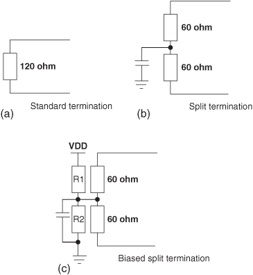
A CAN bus is terminated to minimize signal reflections on the bus. The ISO-11898 requires that the bus has a characteristic impedance of 120 ohms. The bus can be terminated by one of the following methods:
Standard termination
Split termination
Biased split termination
In standard termination, the most common termination method, a 120-ohm resistor is used at each end of the bus, as shown in Figure 9.5(a). In split termination, the ends of the bus are split and a single 60-ohm resistor is used as shown in Figure 9.5(b). Split termination allows for reduced emission, and this method is gaining popularity. Biased split termination is similar to split termination except that a voltage divider circuit and a capacitor are used at either end of the bus. This method increases the EMC performance of the bus (Figure 9.5(c)).
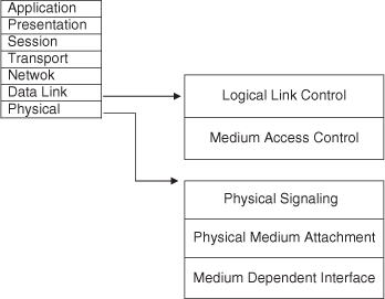
Many network protocols are described using the seven-layer Open Systems Interconnection (OSI) model. The CAN protocol includes the data link layer, and the physical layer of the OSI reference model (see Figure 9.6). The data link layer (DLL) consists of the Logical Link Control (LLC) and Medium Access Control (MAC). LLC manages the overload notification, acceptance filtering, and recovery management. MAC manages the data encapsulation, frame coding, error detection, and serialization/deserialization of the data. The physical layer consists of the physical signaling layer (PSL), physical medium attachment (PMA), and the medium dependent interface (MDI). PSL manages the bit encoding/decoding and bit timing. PMA manages the driver/receiver characteristics, and MDI is the connections and wires.
There are basically four message frames in CAN: data, remote, error, and overload. The data and remote frames need to be set by the user. The other two are set by the CAN hardware.
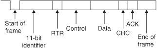
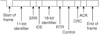
The data frame is in two formats: standard (having an 11-bit ID) and extended (having a 29-bit ID). The data frame is used by the transmitting device to send data to the receiving device, and the data frame is the most important frame handled by the user. Figure 9.7 shows the data frame’s structure. A standard data frame starts with the start of frame (SOF) bit, which is followed by an 11-bit identifier and the remote transmission request (RTR) bit. The identifier and the RTR form the 12-bit arbitration field. The control field is 6 bits wide and indicates how many bytes of data are in the data field. The data field can be 0 to 8 bytes. The data field is followed by the CRC field, which checks whether or not the received bit sequence is corrupted. The ACK field is 2 bits and is used by the transmitter to receive acknowledgment of a valid frame from any receiver. The end of the message is indicated by a 7-bit end of frame (EOF) field. In an extended data frame, the arbitration field is 32 bits wide (29-bit identifier +1-bit IDE to define the message as an extended data frame +1-bit SRR which is unused +1-bit RTR) (see Figure 9.8).
The data frame consists of the following fields:
The start of frame field indicates the beginning of a data frame and is common to both standard and extended formats.
Arbitration is used to resolve bus conflicts that occur when several devices at once start sending messages on the bus. The arbitration field indicates the priority of a frame, and it is different in the standard and extended formats. In the standard format there are 11 bits, and up to 2032 IDs can be set. The extended format ID consists of 11 base IDs plus 18 extended IDs. Up to 2032 × 218 discrete IDs can be set.
During the arbitration phase, each transmitting device transmits its identifier and compares it with the level on the bus. If the levels are equal, the device continues to transmit. If the device detects a dominant level on the bus while it is trying to transmit a recessive level, it quits transmitting and becomes a receiving device. After arbitration only one transmitter is left on the bus, and this transmitter continues to send its control field, data field, and other data.
The process of arbitration is illustrated in Figure 9.9 by an example consisting of three nodes having identifiers:
Node 1: 11100110011 Node 2: 11100111111 Node 3: 11100110001
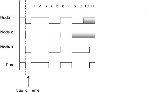
Assuming the recessive level corresponds to 1 and the dominant level to 0, the arbitration is performed as follows:
All the nodes start transmitting simultaneously, first sending SOF bits.
Then they send their identifier bits. The 8th bit of Node 2 is in the recessive state, while the corresponding bits of Nodes 1 and 3 are in the dominant state. Therefore Node 2 stops transmitting and returns to receive mode. The receiving phase is indicated by a gray field.
The 10th bit of Node 1 is in the recessive state, while the same bit of Node 3 is in dominant state. Thus Node 1 stops transmitting and returns to receive mode.
The bus is now left to Node 3, which can send its control and data fields freely.
Notably, the devices on the bus have no addresses. Instead, all the devices pick up all the data on the bus, and every node must filter out the messages it does not want.
The control field is 6 bits wide, consisting of 2 reserved bits and 4 data length code (DLC) bits, and indicates the number of data bytes in the message being transmitted. This field is coded as shown in Table 9.1, where up to 8 transmit bytes can be coded with 6 bits.
The data field carries the actual content of the message. The data size can vary from 0 to 8 bytes. The data is transmitted with the MSB first.
The CRC field, consisting of a 15-bit CRC sequence and a 1-bit CRC delimiter, is used to check the frame for a transmission error. The CRC calculation includes the start of frame, arbitration field, control field, and data field. The calculated CRC and the received CRC sequence are compared, and if they do not match, an error is assumed.
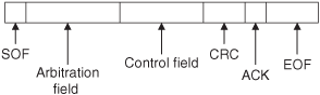
The remote frame is used by the receiving unit to request transmission of a message from the transmitting unit. It consists of six fields (see Figure 9.10): start of frame, arbitration field, control field, CRC field, ACK field, and end of frame field. A remote frame is the same as a data frame except that it lacks a data field.
Error frames are generated and transmitted by the CAN hardware and are used to indicate when an error has occurred during transmission. An error frame consists of an error flag and an error delimiter. There are two types of error flags: active, which consists of 6 dominant bits, and passive, which consists of 6 recessive bits. The error delimiter consists of 8 recessive bits.
The overload frame is used by the receiving unit to indicate that it is not yet ready to receive frames. This frame consists of an overload flag and an overload delimiter. The overload flag consists of 6 dominant bits and has the same structure as the active error flag of the error frame. The overload delimiter consists of 8 recessive bits and has the same structure as the error delimiter of the error frame.
The CAN bus makes use of bit stuffing, a technique to periodically synchronize transmit-receive operations to prevent timing errors between receive nodes. After 5 consecutive bits with the same level, one bit of inverted data is added to the sequence. If, during sending of a data frame or remote frame, the same level occurs in 5 consecutive bits anywhere from the start of frame to the CRC sequence, an inverted bit is inserted in the next (i.e., the sixth) bit. If, during receiving of a data frame or remote frame, the same level occurs in 5 consecutive bits anywhere from the start of frame to CRC sequence, the next (sixth) bit is deleted from the received frame. If the deleted sixth bit is at the same level as the fifth bit, an error (stuffing error) is detected.
The CAN bus identifies five types of errors:
Bit error
CRC error
Form error
ACK error
Stuffing error
Bit errors are detected when the output level and the data level on the bus do not match. Both transmit and receive units can detect bit errors. CRC errors are detected only by receiving units. CRC errors are detected if the calculated CRC from the received message and the received CRC do not match. Form errors are detected by the transmitting or receiving units when an illegal frame format is detected. ACK errors are detected only by the transmitting units if the ACK field is found recessive. Stuffing errors are detected when the same level of data is detected for 6 consecutive bits in any field that should have been bit-stuffed. This error can be detected by both the transmitting and receiving units.
The CAN bus nominal bit rate is defined as the number of bits transmitted every second without resynchronization. The inverse of the nominal bit rate is the nominal bit time. All devices on the CAN bus must use the same bit rate, even though each device can have its own different clock frequency. One message bit consists of four nonoverlapping time segments:
Synchronization segment (Sync_Seg)
Propagation time segment (Prop_Seg)
Phase buffer segment 1 (Phase_Seg1)
Phase buffer segment 2 (Phase_Seg2)
The Sync_Seg segment is used to synchronize various nodes on the bus, and an edge is expected to lie within this segment. The Prop_Seg segment compensates for physical delay times within the network. The Phase_Seg1 and Phase_Seg2 segments compensate for edge phase errors. These segments can be lengthened or shortened by synchronization. The sample point is the point in time where the actual bit value is located and occurs at the end of Phase_Seg1. A CAN controller can be configured to sample three times and use a majority function to determine the actual bit value.
Each segment is divided into units known as time quantum, or TQ. A desired bit timing can be set by adjusting the number of TQ’s that comprise one message bit and the number of TQ’s that comprise each segment in it. The TQ is a fixed unit derived from the oscillator period, and the time quantum of each segment can vary from 1 to 8. The lengths of the various time segments are:
Sync_Seg is 1 time quantum long
Prop_Seg is programmable as 1 to 8 time quanta long
Phase_Seg1 is programmable as 1 to 8 time quanta long
Phase_Seg2 is programmable as 2 to 8 time quanta long
By setting the bit timing, a sampling point can be set so multiple units on the bus can sample messages with the same timing.
The nominal bit time is programmable from a minimum of 8 time quanta to a maximum of 25 time quanta. By definition, the minimum nominal bit time is 1μs, corresponding to a maximum 1Mb/s rate. The nominal bit time (TBIT) is given by:
and the nominal bit rate (NMR) is
The time quantum is derived from the oscillator frequency and the programmable baud rate prescaler, with integer values from 1 to 64. The time quantum can be expressed as:
where TQ is in μs, FOSC is in MHz, and BRP is the baud rate prescaler (0 to 63).
Equation (9.2) can be written as
where TOSC is in μs.
An example of the calculation of a nominal bit rate follows.
Assuming a clock frequency of 20MHz, a baud rate prescaler value of 1, and a nominal bit time of TBIT = 8 * TQ, determine the nominal bit rate.
Using equation (9.3),
TQ = 2 *(1 + 1)/20 = 0.2μs |
also
TBIT = 8 * TQ = 8 * 0.2 = 1.6μs |
From Equation (9.2),
NBR = 1/TBIT = 1/1.6μs = 625,000bites/s or 625Kb/s |
In order to compensate for phase shifts between the oscillator frequencies of nodes on a bus, each CAN controller must synchronize to the relevant signal edge of the received signal. Two types of synchronization are defined: hard synchronization and resynchronization. Hard synchronization is used only at the beginning of a message frame, when each CAN node aligns the Sync_Seg of its current bit time to the recessive or dominant edge of the transmitted start of frame. According to the rules of synchronization, if a hard synchronization occurs, there will not be a resynchronization within that bit time.
With resynchronization, Phase_Seg1 may be lengthened or Phase_Seg2 may be shortened. The amount of change in the phase buffer segments has an upper bound given by the synchronization jump width (SJW). The SJW is programmable between 1 and 4, and its value is added to Phase_Seg1 or subtracted from Phase_Seg2.
In general, any type of PIC microcontroller can be used in CAN bus–based projects, but some PIC microcontrollers (e.g., PIC18F258) have built-in CAN modules, which can simplify the design of CAN bus–based systems. Microcontrollers with no built-in CAN modules can also be used in CAN bus applications, but additional hardware and software are required, making the design costly and also more complex.
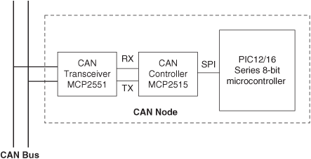
Figure 9.11 shows the block diagram of a PIC microcontroller–based CAN bus application, using a PIC16 or PIC12-type microcontroller (e.g., PIC16F84) with no built-in CAN module. The microcontroller is connected to the CAN bus using an external MCP2515 CAN controller chip and an MCP2551 CAN bus transceiver chip. This configuration is suitable for a quick upgrade to an existing design using any PIC microcontroller.
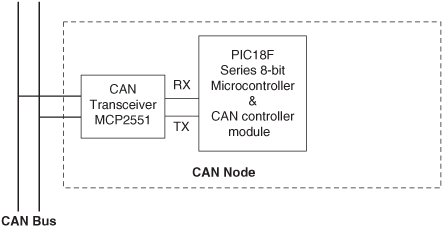
For new CAN bus–based designs it is easier to use a PIC microcontroller with a built-in CAN module. As shown in Figure 9.12, such devices include built-in CAN controller hardware on the chip. All that is required to make a CAN node is to add a CAN transceiver chip. Table 9.2 lists some of the PIC microcontrollers that include a CAN module.
Later in this chapter the PIC18F258 microcontroller is used in a CAN bus–based project. This section describes this microcontroller and its operating principles with respect to its built-in CAN bus. The principles here are in general applicable to other PIC microcontrollers with CAN modules.
The PIC18F258 is a high performance 8-bit microcontroller with integrated CAN module. The device has the following features:
32K flash program memory
1536 bytes RAM data memory
256 bytes EEPROM memory
22 I/O ports
5-channel 10-bit A/D converters
Three timers/counters
Three external interrupt pins
High-current (25mA) sink/source
Capture/compare/PWM module
SPI/I2C module
CAN 2.0A/B module
Power-on reset and power-on timer
Watchdog timer
Priority level interrupts
DC to 40MHz clock input
8 × 8 hardware multiplier
Wide operating voltage (2.0V to 5.5V)
Power-saving sleep mode
The features of the PIC18F258 microcontroller’s CAN module are as follows:
Compatible with CAN 1.2, CAN 2.0A, and CAN 2.0B
Supports standard and extended data frames
Programmable bit rate up to 1Mbit/s
Double-buffered receiver
Three transmit buffers
Two receive buffers
Programmable clock source
Six acceptance filters
Two acceptance filter masks
Loop-back mode for self-testing
Low-power sleep mode
Interrupt capabilities
The CAN module uses port pins RB3/CANRX and RB2/CANTX for CAN bus receive and transmit functions respectively. These pins are connected to the CAN bus via an MCP2551-type CAN bus transceiver chip.
The PIC18F258 microcontroller supports the following frame types:
Standard data frame
Extended data frame
Remote frame
Error frame
Overload frame
Interframe space
A node uses filters to decide whether or not to accept a received message. Message filtering is applied to the whole identifier field, and mask registers are used to specify which bits in the identifier the filters should examine.
The CAN module in the PIC18F258 microcontroller has six modes of operation:
The CAN module is initialized in configuration mode. The module is not allowed to enter configuration mode while a transmission is taking place. In configuration mode the module will neither transmit nor receive, the error counters are cleared, and the interrupt flags remain unchanged.
In disable mode, the module will neither transmit nor receive. In this mode the internal clock is stopped unless the module is active. If the module is active, it will wait for 11 recessive bits on the CAN bus, detect that condition as an IDLE bus, and then accept the module disable command. The WAKIF interrupt (wake-up interrupt) is the only CAN module interrupt that is active in disable mode.
The normal operation mode is the CAN module’s standard operating mode. In this mode, the module monitors all bus messages and generates acknowledge bits, error frames, etc. This is the only mode that can transmit messages.
The listen-only mode allows the CAN module to receive messages, including messages with errors. It can be used to monitor bus activities or to detect the baud rate on the bus. For automatic baud rate detection, at least two other nodes must be communicating with each other. The baud rate can be determined by testing different values until valid messages are received. The listen-only mode cannot transmit messages.
In the loop-back mode, messages can be directed from internal transmit buffers to receive buffers without actually transmitting messages on the CAN bus. This mode is useful during system developing and testing.
The error recognition mode is used to ignore all errors and receive all messages. In this mode, all messages, valid or invalid are received and copied to the receive buffer.
The PIC18F258 microcontroller implements three dedicated transmit buffers: TXB0, TXB1, and TXB2. Pending transmittable messages are in a priority queue. Before the SOF is sent, the priorities of all buffers queued for transmission are compared. The transmit buffer with the highest priority is sent first. If two buffers have the same priority, the one with the higher buffer number is sent first. There are four levels of priority.
Reception of a message is a more complex process. The PIC18F258 microcontroller includes two receive buffers, RXB0 and RXB1, with multiple acceptance filters for each (see Figure 9.13). All received messages are assembled in the message assembly buffer (MAB). Once a message is received, regardless of the type of identifier and the number of data bytes, the entire message is copied into the MAB.
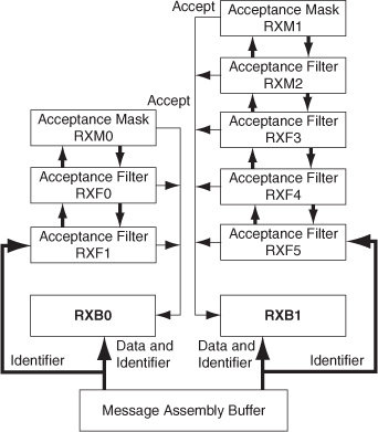
Received messages have priorities. RXB0 is the higher priority buffer, and it has two message acceptance filters, RXF0 and RXF1. RXB1 is the lower priority buffer and has four acceptance filters: RXF2, RXF3, RXF4, and RXF5. Two programmable acceptance filter masks, RXM0 and RXM1, are also available, one for each receive buffer.
The CAN module uses message acceptance filters and masks to determine if a message in the MAB should be loaded into a receive buffer. Once a valid message is received by the MAB, the identifier field of the message is compared to the filter values. If there is a match, that message is loaded into the appropriate receive buffer. The filter masks determine which bits in the identifier are examined with the filters. The truth table in Table 9.3 shows how each bit in the identifier is compared against the masks and filters to determine if the message should be accepted. If a mask bit is set to 0, that bit in the identifier is automatically accepted regardless of the filter bit.
Setting the nodes’ timing parameters is essential for the bus to operate reliably. Given the microcontroller clock frequency and the required CAN bus bit rate, we can calculate the values of the following timing parameters:
Baud rate prescaler value
Prop_Seg value
Phase_Seg1 value
Phase_Seg2 value
SJW value
Correct timing requires that
Prop_Seg + Phase_Seg1 ≥ Phase_Seg2
Phase_Seg2 ≥ SJW
The following example illustrates the calculation of these timing parameters.
Assuming the microcontroller oscillator clock rate is 20MHz and the required CAN bit rate is 125KHz, calculate the timing parameters.
With a 20MHz clock rate, the clock period is 50ns. Choosing a baud rate prescaler value of 4, from Equation (9.4), TQ = 2 * (BRP + 1) * TOSC, gives a time quantum of TQ = 500ns. To obtain a nominal bit rate of 125KHz, the nominal bit time must be:
TBIT = 1/0.125MHz = 8μs, or 16TQ |
The Sync_Segment is 1TQ. Choosing 2TQ for the Prop_Seg, and 7TQ for Phase_Seg1 leaves 6TQ for Phase_Seg2 and places the sampling point at 10TQ at the end of Phase_Seg1.
By the rules described earlier, the SJW can be the maximum allowed (i.e., 4). However, a large SJW is only necessary when the clock generation of different nodes is not stable or accurate (e.g., if ceramic resonators are used). Typically, a SJW of 1 is enough. In summary, the required timing parameters are:
Baud rate prescaler (BRP) = 4
Sync_Seg                  = 1
Prop_Seg                  = 2
Phase_Seg1                = 7
Phase_Seg2                = 6
SJW                       = 1
The sampling point is at 10TQ which corresponds to 62.5% of the total bit time.
There are several tools available for free on the Internet for calculating CAN bus timing parameters. One such tool is the CAN Baud Rate Calculator, developed by Artic Consultants Ltd (http://www.articconsultants.co.uk). An example using this tool follows.
Assuming the microcontroller oscillator clock rate is 20MHz and the required CAN bit rate is 125KHz, calculate the timing parameters using the CAN Baud Rate Calculator.
Figure 9.14 shows the output of the CAN Baud Rate Calculator program. The device type is selected as PIC18Fxxx8, the oscillator frequency is entered as 20MHz, and the CAN bus baud rate is entered as 125KHz.

Clicking the Calculate Settings button calculates and displays the recommended timing parameters. In general, there is more than one solution, and different solutions are given in the Calculated Solutions field’s drop-down menu.
In choosing Solution 2 from the drop-down menu, the following timing parameters are recommended by the program:
Baud rate prescaler (BRP) = 4
Sync_Seg                  = 1
Prop_Seg                  = 5
Phase_Seg1                = 5
Phase_Seg2                = 5
SJW                       = 1
Sample point              = 68%
Error                     = 0%
The mikroC language provides two libraries for CAN bus applications: the library for PIC microcontrollers with built-in CAN modules and the library based on using a SPI bus for PIC microcontrollers having no built-in CAN modules. In this section we will discuss only the library functions available for PIC microcontrollers with built-in CAN modules. Similar functions are available for the PIC microcontrollers with no built-in CAN modules.
The mikroC CAN functions are supported only by PIC18XXX8 microcontrollers with MCP2551 or similar CAN transceivers. Both standard (11 identifier bits) and extended format (29 identifier bits) messages are supported.
The following mikroC functions are provided:
CANSetOperationMode
CANGetOperationMode
CANInitialize
CANSetBaudRAte
CANSetMask
CANSetFilter
CANRead
CANWrite
The CANSetOperationMode function sets the CAN operation mode. The function prototype is:
void CANSetOperationMode(char mode, char wait_flag)
The parameter wait_ flag is either 0 or 0 × FF. If it is set to 0 × FF, the function blocks and will not return until the requested mode is set. If it is set to 0, the function returns as a nonblocking call.
The mode can be one of the following:
The CANGetOperationMode function returns the current CAN operation mode. The function prototype is:
char CANGetOperationMode(void)The CANInitialize function initializes the CAN module. All mask registers are cleared to 0 to allow all messages. Upon execution of this function, the normal mode is set. The function prototype is:
void CANInitialize(char SJW, char BRP, char PHSEG1, char PHSEG2,
char PROPEG, char CAN_CONFIG_FLAGS)
where
SJW | is the synchronization jump width |
BRP | is the baud rate prescaler |
PHSEG1 | is the Phase_Seg1 timing parameter |
PHSEG2 | is the Phase_Seg2 timing parameter |
PROPSEG | is the Prop_Seg |
CAN_CONFIG_FLAGS can be one of the following configuration flags:
| Default flags |
| Use supplied PHSEG2 value |
| Use maximum of PHSEG1 or information processing time (IPT), whichever is greater |
| Use CAN bus line filter for wake-up |
| Do not use CAN bus line filter |
Sample bus once at sample point | |
| Sample bus three times prior to sample point |
| Accept only standard identifier messages |
| Accept only extended identifier messages |
| Use double buffering to receive data |
| Do not use double buffering |
| Accept all messages including invalid ones |
| Accept only valid extended identifier messages |
| Accept only valid standard identifier messages |
| Accept all valid messages |
These configuration values can be bitwise AND’ed to form complex configuration values.
The CANSetBaudRate function is used to set the CAN bus baud rate. The function prototype is:
void CANSetBaudRate(char SJW, char BRP, char PHSEG1, char PHSEG2,
char PROPSEG, char CAN_CONFIG_FLAGS)
The arguments of the function are as in function CANInitialize.
The CANSetMask function sets the mask for filtering messages. The function prototype is:
void CANSetMask(char CAN_MASK, long value, char
CAN_CONFIGFLAGS)
CAN_MASK can be one of the following:
| Receive buffer 1 mask value |
| Receive buffer 2 mask value |
value is the mask register value. CAN_CONFIG_FLAGS can be either CAN_CONFIG_XTD (extended message), or CAN_CONFIG_STD (standard message).
The CANSetFilter function sets filter values. The function prototype is:
void CANSetFilter(char CAN_FILTER, long value, char
CAN_CONFIG_FLAGS)
CAN_FILTER can be one of the following:
| Filter 1 for buffer 1 |
| Filter 2 for buffer 1 |
| Filter 1 for buffer 2 |
| Filter 2 for buffer 2 |
| Filter 3 for buffer 2 |
| Filter 4 for buffer 2 |
CAN_CONFIG_FLAGS can be either CAN_CONFIG_XTD (extended message) or CAN_CONFIG_STD (standard message).
The CANRead function is used to read messages from the CAN bus. If no message is available, 0 is returned. The function prototype is:
char CANRead(long *id, char *data, char *datalen, char
*CAN_RX_MSG_FLAGS)
id is the CAN message identifier. Only 11 or 29 bits may be used depending on message type (standard or extended). data is an array of bytes up to 8 where the received data is stored. datalen is the length of the received data (1 to 8).
CAN_RX_MSG_FLAGS can be one of the following:
| Receive buffer filter 1 accepted this message |
| Receive buffer filter 2 accepted this message |
| Receive buffer filter 3 accepted this message |
| Receive buffer filter 4 accepted this message |
| Receive buffer filter 5 accepted this message |
| Receive buffer filter 6 accepted this message |
| Receive buffer overflow occurred |
| Invalid message received |
| Extended identifier message received |
| RTR frame message received |
| This message was double buffered |
These flags can be bitwise AND’ed if desired.
The CANWrite function is used to send a message to the CAN bus. A zero is returned if message can not be queued (buffer full). The function prototype is:
char CANWrite(long id, char*data, char datalen, char
CAN_TX_MSG_FLAGS)
id is the CAN message identifier. Only 11 or 29 bits may be used depending on message type (standard or extended). data is an array of bytes up to 8 where the data to be sent is stored. datalen is the length of the data (1 to 8).
CAN_TX_MSG_FLAGS can be one of the following:
| Transmit priority 0 |
| Transmit priority 1 |
| Transmit priority 2 |
| Transmit priority 3 |
| Standard identifier message |
| Extended identifier message |
| Non RTR message |
| RTR message |
These flags can be bitwise AND’ed if desired.
To operate the PIC18F258 microcontroller on the CAN bus, perform the following steps:
Configure the CAN bus I/O port directions (RB2 and RB3)
Initialize the CAN module (CANInitialize)
Set the CAN module to CONFIG mode (CANSetOperationMode)
Set the mask registers (CANSetMask)
Set the filter registers (CANSetFilter)
Set the CAN module to normal mode (CANSetOperationMode)
Write/read data (CANWrite/CANRead)
The following is a simple two-node CAN bus–based project. The block diagram of the project is shown in Figure 9.15. The system is made up of two CAN nodes. One node (called DISPLAY node) requests the temperature every second and displays it on an LCD. This process is repeated continuously. The other node (called COLLECTOR node) reads the temperature from an external semiconductor temperature sensor.
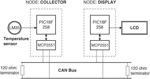
The project’s circuit diagram is given in Figure 9.16. Two CAN nodes are connected together using a two-meter twisted pair cable, terminated with a 120-ohm resistor at each end.
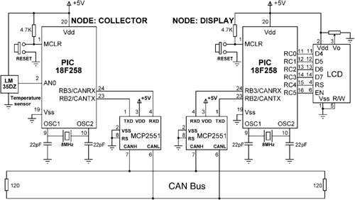
Like the COLLECTOR processor, the DISPLAY processor consists of a PIC18F258 microcontroller with a built-in CAN module and an MCP2551 transceiver chip. The microcontroller is operated from an 8MHz crystal. The MCLR input is connected to an external reset button. The CAN outputs (RB2/CANTX and RB3/CANRX) of the microcontroller are connected to the TXD and RXD inputs of the MCP2551. Pins CANH and CANL of the transceiver chip are connected to the CAN bus. An HD44780-type LCD is connected to PORTC of the microcontroller to display the temperature values.
The COLLECTOR processor consists of a PIC18F258 microcontroller with a built-in CAN module and an MCP2551 transceiver chip. The microcontroller is operated from an 8MHz crystal. The MCLR input is connected to an external reset button. Analog input AN0 of the microcontroller is connected to a LM35DZ-type semiconductor temperature sensor. The sensor can measure temperature in the range of 0°C to 100°C and generates an analog voltage directly proportional to the measured temperature (i.e., the output is 10mV/°C). For example, at 20°C the output voltage is 200mV.
The CAN outputs (RB2/CANTX and RB3/CANRX) of the microcontroller are connected to the TXD and RXD inputs of an MCP2551-type CAN transceiver chip. The CANH and CANL outputs of this chip are connected directly to a twisted cable terminating at the CAN bus. The MCP2551 is an 8-pin chip that supports data rates up to 1Mb/s. The chip can drive up to 112 nodes. An external resistor connected to pin 8 of the chip controls the rise and fall times of CANH and CANL so that EMI can be reduced. For high-speed operation this pin should be connected to ground. A reference voltage equal to VDD/2 is output from pin 5 of the chip.
The program listing is in two parts: the DISPLAY program and the COLLECTOR program. The operation of the system is as follows:
The DISPLAY processor requests the current temperature from the COLLECTOR processor over the CAN bus
The COLLECTOR processor reads the temperature, formats it, and sends to the DISPLAY processor over the CAN bus
The DISPLAY processor reads the temperature from the CAN bus and then displays it on the LCD
This process is repeated every second
Figure 9.17 shows the program listing of the DISPLAY program, called DISPLAY.C. At the beginning of the program PORTC pins are configured as outputs, RB3 is configured as input (CANRX), and RB2 is configured as output (CANTX). In this project the CAN bus bit rate is selected as 100Kb/s. With a microcontroller clock frequency of 8MHz, the Baud Rate Calculator program (see Figure 9.14) is used to calculate the timing parameters as:
SJW = 1
BRP = 1
Phase_Seg1 = 6
Phase_Seg2 = 7
Prop_Seg = 6
Table 9.17. DISPLAY program listing
/********************************************************************** CAN BUS EXAMPLE - NODE: DISPLAY ===============================This is the DISPLAY node of the CAN bus example. In this project a PIC18F258type microcontroller is used. An MCP2551 type CAN bus transceiver is used toconnect the microcontroller to the CAN bus. The microcontroller is operated froman 8MHz crystal with an external reset button.Pin CANRX and CANTX of the microcontroller are connected to pins RXDand TXD of the transceiver chip respectively. Pins CANH and CANL ofthe transceiver chip are connected to the CAN bus.An LCD is connected to PORTC of the microcontroller. The ambienttemperature is read from another CAN node and is displayed on the LCD.The LCD is connected to the microcontroller as follows:Microcontroller LCD RC0 D4 RC1 D5 RC2 D6 RC3 D7 RC4 RS RC5 ENCAN speed parameters are: Microcontroller clock: 8MHz CAN Bus bit rate: 100Kb/s Sync_Seg: 1 Prop_Seg: 6 Phase_Seg1: 6 Phase_Seg2: 7 SJW: 1 BRP: 1 Sample point: 65%Author: Dogan IbrahimDate: October 2007File: DISPLAY.C***********************************************************************/void main(){ unsigned char temperature, data[8]; unsigned short init_flag, send_flag, dt, len, read_flag; char SJW, BRP, Phase_Seg1, Phase_Seg2, Prop_Seg, txt[4]; long id, mask; |
The mikroC CAN bus function CANInitialize is used to initialize the CAN module. The timing parameters and the initialization flag are specified as arguments in this function. The initialization flag is made up from the bitwise AND of:
init_flag = CAN_CONFIG_SAMPLE_THRICE &
            CAN_CONFIG_PHSEG2_PRG_ON &
            CAN_CONFIG_STD_MSG &
            CAN_CONFIG_DBL_BUFFER_ON &
            CAN_CONFIG_VALID_XTD_MSG &
            CAN_CONFIG_LINE_FILTER_OFF;
Where sampling the bus three times is specified, the standard identifier is specified, double buffering is turned on, and the line filter is turned off.
Then the operation mode is set to CONFIG and the filter masks and filter values are specified. Both mask 1 and mask 2 are set to all 1’s (−1 is a shorthand way of writing hexadecimal FFFFFFFF, i.e., setting all mask bits to 1’s) so that all filter bits match up with incoming data.
Filter 3 for buffer 2 is set to value 3 so that identifiers having values 3 are accepted by the receive buffer.
The operation mode is then set to NORMAL. The program then configures the LCD and displays the message “CAN BUS” for one second on the LCD.
The main program loop executes continuously and starts with a for statement. Inside this loop the LCD is cleared and text “TEMP =” is displayed on the LCD. Then character “T” is sent over the bus with the identifier equal to 500 (the COLLECTOR node filter is set to accept identifier 500). This is a request to the COLLECTOR node to send the temperature reading. The program then reads the temperature from the CAN bus, converts it to a string in array txt, and displays it on the LCD. This process repeats after a one-second delay.
Figure 9.18 shows the program listing of the COLLECTOR program, called COLLECTOR.C. The initial part of this program is the same as the DISPLAY program. The receive filter is set to 500 so that messages with identifier 500 are accepted by the program.
Table 9.18. COLLECTOR program listing
/*********************************************************************** CAN BUS EXAMPLE - NODE: COLLECTOR =================================This is the COLLECTOR node of the CAN bus example. In this project aPIC18F258 type microcontroller is used. An MCP2551 type CAN bus transceiveris used to connect the microcontroller to the CAN bus. The microcontroller isoperated from an 8MHz crystal with an external reset button.Pin CANRX and CANTX of the microcontroller are connected to pins RXDand TXD of the transceiver chip respectively. Pins CANH and CANL of thetransceiver chip are connected to the CAN bus.An LM35DZ type analog temperature sensor is connected to port AN0 of themicrocontroller. The microcontroller reads the temperature when a request isreceived and then sends the temperature value as a byte to Node:DISPLAY onthe CAN bus.CAN speed parameters are: Microcontroller clock: 8MHz CAN Bus bit rate: 100Kb/s Sync_Seg: 1 Prop_Seg: 6 Phase_Seg1: 6 Phase_Seg2: 7 SJW: 1 BRP: 1 Sample point: 65%Author: Dogan IbrahimDate: October 2007File: COLLECTOR.C***********************************************************************/void main(){ unsigned char temperature, data[8]; unsigned short init_flag, send_flag, dt, len, read_flag; char SJW, BRP, Phase_Seg1, Phase_Seg2, Prop_Seg, txt[4]; unsigned int temp; unsigned long mV; long id, mask; TRISA = 0xFF; // PORTA are inputs TRISB = 0x08; // RB2 is output, RB3 is input//// Configure A/D converter// ADCON1 = 0x80; |
Inside the program loop, the program waits until it receives a request to send the temperature. Here the request is identified by the reception of character “T”. Once a valid request is received, the temperature is read and converted into °C (stored in variable temperature) and then sent to the CAN bus as a byte with an identifier value equal to 3. This process repeats forever.
Figure 9.19 summarizes the operation of both nodes.
