
In this and the remaining chapters we will look at the design of more complex PIC18 microcontroller–based projects. This chapter discusses the design of Secure Digital (SD) memory card–based projects. The remaining chapters of the book describe the basic theory and design of projects based on the popular USB bus and CAN bus protocols.
Before going into the design details of SD card–based projects, we should take a look at the basic principles and operation of SD card memory devices. Figure 7.1 shows a typical SD card.
The SD card is a flash memory storage device designed to provide high-capacity, nonvolatile, and rewritable storage in a small size. These devices are frequently used in many electronic consumer goods, such as cameras, computers, GPS systems, mobile phones, and PDAs. The memory capacity of the SD cards is increasing all the time. Currently they are available at capacities from 256MB to 8GB. The SD cards come in three sizes: standard, mini, and micro. Table 7.1 lists the main specifications of the most common standard SD and miniSD cards.
SD card specifications are maintained by the SD Card Association, which has over six hundred members. MiniSD and microSD cards are electrically compatible with the standard SD cards and can be inserted in special adapters and used as standard SD cards in standard card slots.
SD card speeds are measured three different ways: in KB/s (kilobytes per second), in MB/s (megabytes per second), in an “x” rating similar to that of CD-ROMS where “x” is the speed corresponding to 150KB/s. The various “x” based speeds are:
4x: 600KB/s
16x: 2.4MB/s
40x: 6.0MB/s
66x: 10MB/s
In this chapter we are using the standard SD card only. The specifications of the smaller SD cards are the same and are not described further in this chapter.
SD cards can be interfaced to microcontrollers using two different protocols: SD card protocol and the SPI (Serial Peripheral Interface) protocol. The SPI protocol, being more widely used, is the one used in this chapter. The standard SD card has 9 pins with the pin layout shown in Figure 7.2. The pins have different functions depending on the interface protocol. Table 7.2 gives the function of each pin in both the SD and SPI modes of operation.

Table 7.2. Standard SD card pin definitions
Pin | Name | SD description | SPI description |
|---|---|---|---|
1 | CD/DAT3/CS | Data line 3 | Chip select |
2 | CMD/Datain | Command/response | Host to card command and data |
3 | VSS | Supply ground | Supply ground |
4 | VDD | Supply voltage | Supply voltage |
5 | CLK | Clock | Clock |
6 | VSS2 | Supply voltage ground | Supply voltage ground |
7 | DAT0 | Data line 0 | Card to host data and status |
8 | DAT1 | Data line 1 | Reserved |
9 | DAT2 | Data line 2 | Reserved |
Since the SD card projects described in this chapter are based on the SPI bus protocol, it is worth looking at the specifications of this bus before proceeding to the projects themselves.
The SPI (Serial Peripheral Interface) bus is a synchronous serial bus standard named by Motorola that operates in full duplex mode. Devices on a SPI bus operate in master-slave mode, where the master device initiates the data transfer, selects a slave, and provides a clock for the slaves. The selected slave responds and sends its data to the master at each clock pulse. The SPI bus can operate with a single master device and one or more slave devices. This simple interface is also called a “four-wire” interface.
The signals in the SPI bus are named as follows:
MOSI—master output, slave input
MISO—master input, slave output
SCLK—serial clock
SS—slave select
These signals are also named as:
DO—data out
DI—data in
CLK—clock
CD—chip select
Figure 7.3 shows the basic connection between a master device and a slave device in SPI bus. The master sends out data on line MOSI and receives data on line MISO. The slave must be selected before data transfer can take place.

Figure 7.4 shows an instance where more than one slave device is connected to the SPI bus. Here, each slave is selected individually by the master, and although all the slaves receive the clock pulses, only the selected slave device responds. If an SPI device is not selected, its data output goes into a high-impedance state so it does not interfere with the currently selected device on the bus.

Data transmission normally occurs in and out of the master and slave devices as the master supplies clock pulses. To begin a communication, the master first pulls the slave select line low for the desired slave device. Then the master issues clock pulses, and during each SPI clock cycle, a full duplex data transmission occurs. When there are no more data to be transmitted, the master stops toggling its clock output.
The SPI bus is currently used by microcontroller interface circuits to talk to a variety of devices such as:
Memory devices (SD cards)
Sensors
Real-time clocks
Communications devices
Displays
The advantages of the SPI bus are:
Simple communication protocol
Full duplex communication
Very simple hardware interface
Its disadvantages are:
Requires four pins
No hardware flow control
No slave acknowledgment
It is worth remarking that there are no SPI standards governed by an international committee, so there are several versions of SPI bus implementation. In some applications, the MOSI and MISO lines are combined into a single data line, thereby reducing the line requirements to three. Some implementations have two clocks, one to capture (or display) data and the other to clock it into the device. Also, in some implementations the chip select line may be active-high rather than active-low.
When the SD card is operated in SPI mode, only seven pins are used. Three (pins 3, 4, and 6) are used for the power supply, leaving four pins (pins 1, 2, 5, and 7) for the SPI mode of operation:
Two power supply ground (pins 3 and 6)
Power supply (pin 4)
Chip select (pin 1)
Data out (pin 7)
Data in (pin 2)
CLK (pin 5)
At power-up, the SD card defaults to the SD bus protocol. The card is switched to SPI mode if the Chip Select (CS) signal is asserted during reception of the reset command. When the card is in SPI mode, it only responds to SPI commands. The host may reset a card by switching the power supply off and then on again.
The mikroC compiler provides a library of commands for initializing, reading, and writing to SD cards. It is not necessary to know the internal structure of an SD card in detail before using one, since the library functions are available. However, a basic understanding of the internal structure of an SD card is helpful in making the best use of the card. In this section we will look briefly at the internal architecture and operation of SD cards.
An SD card has a set of registers that provide information about the status of the card. When the card is operated in SPI mode these are:
Card identification register (CID)
Card specific data register (CSD)
SD configuration register (SCR)
Operation control register (OCR)
The CID register consists of 16 bytes and contains the manufacturer ID, product name, product revision, card serial number, manufacturer date code, and a checksum byte. Table 7.3 shows the structure of the CID register.
Table 7.3. Structure of the CID register
Name | Type | Width | Comments |
|---|---|---|---|
Manufacturer ID (MID) | Binary | 1 byte | Manufacturer ID (e.g., 0×03 for SanDisk) |
OEM/Application ID (OID) | ASCII | 2 bytes | Identifies card OEM and/or card contents |
Product Name (PNM) | ASCII | 5 bytes | Product name |
Product Revision (PRV) | BCD | 1 byte | Two binary coded digits |
Serial Number (PSN) | Binary | 4 bytes | 32 bits unsigned integer |
Reserved | 4 bits | Upper 4 bits | |
Manufacture Date Code (MDT) | BCD | 12 bits | Manufacture date (offset from 2000) |
CRC-7 Checksum | Binary | 7 bits | Checksum |
Not used | Binary | 1 bit | Always 1 |
The CSD register consists of 16 bytes and contains card-specific data such as the card data transfer rate, read/write block lengths, read/write currents, erase sector size, file format, write protection flags, and checksum. Table 7.4 shows the structure of the CSD register.
Table 7.4. Structure of the CSD register
Byte 0 | 0 0 XXXXXX |
Byte 1 | TAAC [7:0] |
Byte 2 | NSAC [7:0] |
Byte 3 | TRAN_SPEED [7:0] |
Byte 4 | CCC [11:4] |
Byte 5 | CCC [3:0] READ_BL_LEN [3:0] |
Byte 6 | READ_BL_PARTIAL WRITE_BLK_MISALIGN READ_BLK_MISALIGN DSR_IMP X X C_SIZE (11:10) |
Byte 7 | C_SIZE [9:2] |
Byte 8 | C_SIZE [1:0] VDD_R_CURR_MIN (2:0) VDD_R_CURR_MAX (2:0) |
Byte 9 | VDD_W_CURR_MIN (2:0) VDD_W_CURR_MAX (2:0) C_SIZE_MULT (2:1) |
Byte 10 | ERASE_BLK_EN SECTOR_SIZE (6:1) |
Byte 11 | SECTOR_SIZE (0) WP_GRP_SIZE (6:0) |
Byte 12 | WP_GRP_ENABLE X X R2W_FACTOR(2:0) |
Byte 13 | WRITE_BL_LEN (1:0) 0 X X X X X |
Byte 14 | FILE_FORMAT_GRP COPY PERM_WRITE_PROTECT TMP_WRITE_PROTECT FILE_FORMAT (1:0) X X |
Byte 15 | CRC (6:0) 1 |
Field definitions | |
TAAC | data read access time 1 (e.g., 1.5ms) |
NSAC | data read access time in CLK cycles |
TRAN_SPEED | max data transfer rate |
CCC | card command classes |
READ_BL_LEN | max read data block length (e.g., 512 bytes) |
READ_BL_PARTIAL | partial blocks for read allowed |
WRITE_BLK_MISALIGN | write block misalignment |
READ_BLK_MISALIGN | read block misalignment |
DSR_IMP | DSR implemented |
C_SIZE | device size |
VDD_R_CURR_MIN | max read current at VDD min |
VDD_R_CURR_MAX | max read current at VDD max |
VDD_W_CURR_MIN | max write current at VDD min |
VDD_W_CURR_MAX | max write current at VDD max |
C_SIZE_MULT | device size multiplier |
ERASE_BLK_EN | erase single block enable |
SECTOR_SIZE | erase sector size |
WP_GRP_SIZE | write protect group size |
WP_GRP_ENABLE | write protect group enable |
R2W_FACTOR | write speed factor |
WRITE_BL_LEN | max write data block length (e.g., 512 bytes) |
WRITE_BL_PARTIAL | partial blocks for write allowed |
FILE_FORMAT_GRP | file format group |
COPY | copy flag |
PERM_WRITE_PROTECT | permanent write protect |
TMP_WRITE_PROTECT | temporary write protect |
FILE_FORMAT | file format |
The SCR register is 8 bytes long and contains information about the SD card’s special features and capabilities, such as security support and data bus widths supported.
The OCR register is only 4 bytes long and stores the VDD voltage profile of the card. The OCR shows the voltage range in which the card data can be accessed.
All SD-card SPI commands are 6 bytes long, with the MSB transmitted first. Figure 7.5 shows the command format. The first byte is known as the command byte, and the remaining five bytes are called command arguments. Bit 6 of the command byte is set to 1 and the MSB bit is always 0. With the remaining six bits we have sixty-four possible commands, named CMD0 to CMD63. Some of the important commands are:
• | CMD0 | GO_IDLE_STATE (resets the SD card) |
• | CMD1 | SEND_OP_COND (initializes the card) |
• | CMD9 | SEND_CSD (gets CSD register data) |
• | CMD10 | SEND_CID (gets CID register data) |
• | CMD16 | SET_BLOCKLEN (selects a block length in bytes) |
• | CMD17 | READ_SINGLE_BLOCK (reads a block of data) |
• | CMD24 | WRITE_BLOCK (writes a block of data) |
• | CMD32 | ERASE_WR_BLK_START_ADDR (sets the address of the first write block to be erased) |
• | CMD33 | ERASE_WR_BLK_END_ADDR (sets the address of the last write block to be erased) |
• | CMD38 | ERASE (erases all previously selected blocks) |
In response to a command, the card sends a status byte known as R1. The MSB bit of this byte is always 0 and the other bits indicate the following error conditions:
Card in idle state
Erase reset
Illegal command
Communication CRC error
Erase sequence error
Address error
Parameter error
The SD card in SPI mode supports single-block and multiple-block read operations. The host should set the block length. After a valid read command the card responds with a response token, followed by a data block and a CRC check. The block length can be between 1 and 512 bytes. The starting address can be any valid address in the address range of the card.
In multiple-block read operations, the card sends data blocks with each block having its own CRC check attached to the end of the block.
The SD card in SPI mode supports single- or multiple-block write operations. After receiving a valid write command from the host, the card responds with a response token and waits to receive a data block. A one-byte “start block” token is added to the beginning of every data block. After receiving the data block the card responds with a “data response” token, and the card is programmed as long as the data block is received with no errors.
In multiple-block write operations the host sends the data blocks one after the other, each preceded by a “start block” token. The card sends a response byte after receiving each data block.
SD cards are available in various sizes. At the time of writing, SanDisk Corporation (www.sandisk.com) offered the models and capacities shown in Table 7.5. The company may now be offering models with 4GB or even greater capacity.
In addition to the normal storage area on the card, there is also a protected area pertaining to the secured copyright management. This area can be used by applications to save security-related data and can be accessed by the host using secured read/write commands. The card write protection mechanism does not affect this area. Table 7.6 shows the size of the protected area and the data area available to the user for reading and writing data. For example, a 1GB card has 20,480 blocks (one block is 512 bytes) of protected area and 1,983,744 blocks of user data area.
Data can be written to or read from any sector of the card using raw sector access methods. In general, SD card data is structured as a file system and two DOS-formatted partitions are placed on the card: the user area and the security protected area. The size of each area is shown in Table 7.7. For example, in a 1GB card, the size of the security protected area is 519 sectors (1 sector is 512 bytes), and the size of the user data area is 1,982,976 sectors.
A card can be inserted and removed from the bus without any damage. This is because all data transfer operations are protected by cyclic redundancy check (CRC) codes, and any bit changes caused by inserting or removing a card can easily be detected. SD cards typically operate with a supply voltage of 2.7V. The maximum allowed power supply voltage is 3.6V. If the card is to be operated from a standard 5.0V supply, a voltage regulator should be used to drop the voltage to 2.7V.
Using an SD card requires the card to be inserted into a special card holder with external contacts (see Figure 7.6) so connections are easily made to the required card pins.

The mikroC language provides an extensive set of library functions to read and write data to SD cards (and also MultiMediaCards, MMC). Data can be written to or read from a given sector of the card, or the file system on the card can be used for more sophisticated applications.
The following library functions are provided:
| (initialize the card) |
| (read one sector of data) |
| (write one sector of data) |
| (read CID register) |
| (read CSD register) |
| (initialize FAT) |
| (format the card to FAT16) |
| (assign the file we will be working with) |
| (reset the file pointer; opens the currently assigned file for reading) |
| (reset the file pointer and clear assigned file; opens the assigned file for writing) |
| (move file pointer to the end of assigned file so new data can be appended to the file) |
| (read the byte the file pointer points to) |
| (write a block of data to the assigned file) |
| (write system timestamp to a file) |
| (delete a file) |
| (read file timestamp) |
| (get file size in bytes) |
| (create a swap file) |
In the remainder of this chapter we will look at some SD-card and PIC18 microcontroller-based projects.
In this project a SD card is interfaced to a PIC18F452-type microcontroller. The serial output port of the microcontroller is connected to the serial input port (e.g., COM1) of a PC. The microcontroller reads the contents of the card CID register and sends this data to the PC so it can be displayed on the PC screen.
Figure 7.7 shows the block diagram of the project.

The circuit diagram of the project is shown in Figure 7.8. The SD card is inserted into a card holder and then connected to PORTC of a PIC18F452 microcontroller through 2.2K and 3.3K resistors, using the following pins:
Card CS to PORTC pin RC2
Card CLK to PORTC pin RC3
Card DO to PORTC pin RC4
Card DI to PORTC pin RC5

According to the SD card specifications, when the card is operating with a supply voltage of VDD = 3.3V, the input-output pin voltage levels are as follows:
Minimum produced output HIGH voltage, VOH = 2.475V
Maximum produced output LOW voltage, VOL = 0.4125V
Minimum required input HIGH voltage, VIH = 2.0625
Maximum input HIGH voltage, VIH = 3.6V
Maximum required input LOW voltage, VIL = 0.825V
Although the output produced by the card (2.475V) is sufficient to drive the input port of a PIC microcontroller, the logic HIGH output of the microcontroller (about 4.3V) is too high for the SD card inputs (maximum 3.6V). Therefore, a potential divider is set up at the three inputs of the SD card using 2.2K and 3.3K resistors. This limits the maximum voltage at the inputs of the SD card to about 2.5V:
SD card input voltage = 4.3V × 3.3K/(2.2K + 3.3K) = 2.48V |
Serial output port pin RC6 (TX) of the microcontroller is connected to a MAX232-type RS232 voltage level converter chip and then to a 9-way D-type connector so it can be connected to the serial input port of a PC.
The microcontroller is powered from a 5V supply which is obtained via a 7805-type 5V regulator with a 9V input. The 2.7V–3.6V supply required by the SD card is obtained via an MC33269DT-3.3 regulator with 3.3V output and is driven from the 5V input voltage.
The program listing of the project is given in Figure 7.9 (program SD1.C). At the beginning of the main program, character array CID is declared to have 16 bytes.
Table 7.9. Program listing
/************************************************************** SD CARD PROJECT =============In this project a SD card is connected to PORTC as follows: CS RC2 CLK RC3 DO RC4 DI RC5In addition, a MAX232 type RS232 voltage level converter chipis connected to serial output port RC6.The program reads the SD card CID register parameters andsends it to a PC via the serial interface. This process isrepeated at every 10 seconds.The UART is set to operate at 2400 Baud, 8 bits, no parity.Author: Dogan IbrahimDate: August 2007File: SD1.C**************************************************************///// This function sends carriage-return and line-feed to USART//void Newline(){ Soft_Uart_Write(0x0D); // Send carriage-return Soft_Uart_Write(0x0A); // Send line-feed}//// This function sends a space character to USART// void Space(){ Soft_Uart_Write(0x20);}//// This function sends a text to serial port//void Text_To_Usart(unsigned char *m){ unsigned char i; |
Variable msg is loaded with the message that is to be displayed when power is applied to the system. Then the UART is initialized at PORTC with a baud rate of 2400.
Before the SD card library functions are used, the function Spi_Init_Advanced must be called with the given arguments. Then the SD card bus is initialized by calling function Mmc_Init, where it is specified that the card is connected to PORTC. The program then enters an endless loop that repeats every ten seconds. Inside this loop the heading message is displayed followed by two new-line characters. The program then reads the contents of register CID by calling function Mmc_Read_Cid and stores the data in character array CID. The data is then sent to the serial port by calling function Str_To_Usart. At the end of the loop two new-line characters are displayed, the program waits for ten seconds, and the loop is repeated.
The operation of the project can be tested by connecting the device to a PC and starting the HyperTerminal terminal emulation program on the PC. Set the communications parameters to 2400 baud, 8 data bits, 1 stop bit, and no parity bit. An example output on the screen is shown in Figure 7.10.
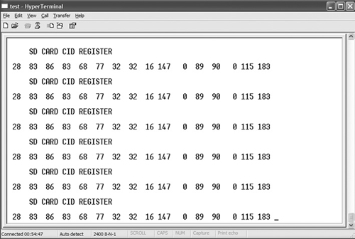
The data returned by the card is:
28 83 86 83 68 77 32 32 16 147 0 89 90 0 115 183
Referring to Table 7.3, we can say the following about this card:
Manufacturer ID | = | 28 decimal |
OEM/Application ID | = | SV |
Product Name | = | SDM |
Product Revision | = | 1.0 (decimal 16 corresponds to binary “0001 0000” which is 10 in BCD; the revision number is as n.m, giving 1.0) |
Serial Number | = | 16 147 0 89 decimal |
= | “0000” bits (4 bits only) | |
Manufacture Date Code | = | 073 (this 12-bit parameter has the binary value “0000 0111 0011” where the upper 4 bits are derived from the lower 4 bits of the reserved field and the lower 8 bits are decimal 115. This gives BCD value 073. The date is in YYM format since 2000. Thus, this card was manufactured in 2007, March). |
CRC | = | “1011100” binary (the LSB bit is always 1) |
The hardware of this project is the same as for Project 7.1 (i.e., as shown in Figure 7.8). In this project, sector 10 of the SD card is filled with “C” characters, and then this sector is read and the card data is sent to the UART.
The program listing of this project is given in Figure 7.11 (program SD2.C). Two character arrays called data1 and data2, of 512 bytes each, are declared at the beginning of the program. Array data1 is loaded with character “C,” and the contents of this array are written to sector 10 of the SD card. Then the contents of sector 10 are read into character array data2 and sent to the UART, displaying 512 “C” characters on the PC screen. Normally, only one array is used to read and write to the SD card. Two arrays are used here to make it clear that what is sent to the UART is the card data, not the contents of array data1.
Table 7.11. Program listing of the project
/************************************************************** SD CARD PROJECT ===============In this project a SD card is connected to PORTC as follows: CS RC2 CLK RC3 DO RC4 DI RC5In addition, a MAX232 type RS232 voltage level converter chipis connected to serial output port RC6.The program loads sector 10 of the SD card with character “C”.The contents of sector 10 is then read and sent to the UART,displaying 512 “C” characters on the PC display.Author: Dogan IbrahimDate: August 2007File: SD2.C**************************************************************/unsigned char data1[512],data2[512];unsigned int i;unsigned short x;void main(){//// Configure the serial port// Usart_Init(2400);//// Initialise the SD card// Spi_Init_Advanced(MASTER_OSC_DIV16,DATA_SAMPLE_MIDDLE, CLK_IDLE_LOW, LOW_2_HIGH);//// Initialise the SD bus// while(Mmc_Init(&PORTC,2));//// Fill buffer with character “C”// for(i=0; i<512; i++)data1[i] = ‘C’;//// Write to sector 10// x = Mmc_Write_Sector(10, data1); |
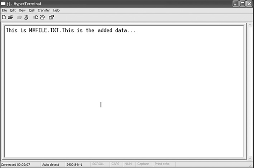
The hardware of this project is the same as for Project 7.1 (i.e., as shown in Figure 7.8). In this project, a file called MYFILE55.TXT is created on the SD card. String “This is MYFILE.TXT” is written to the file initially. Then the string “This is the added data...” is appended to the file. The program then reads the contents of the file and sends the string “This is MYFILE.TXT. This is the added data...” to the UART, enabling the data to be displayed on the PC screen when HyperTerminal is run.
The program listing of the project is given in Figure 7.12 (program SD3.C). At the beginning of the program the UART is initialized to 2400 baud. Then the SPI bus and the FAT file system are initialized as required by the library. The program then creates file MYFILE55.TXT by calling library function Mmc_Fat_Assign with the arguments as the filename and the creation flag 0×80, which tells the function to create a new file if the file does not exist. The filename should be in “filename.extension” format, though it is also possible to specify an eight-digit filename and a three-digit extension with no “.” between them, as the “.” will be inserted by the function. Other allowed values of the creation flag are given in Table 7.8. Note that the SD card must have been formatted in FAT16 before we can read or write to it. Most new cards are already formatted, but we can also use the Mmc_Fat_QuickFormat function to format a card.
Table 7.12. Program listing of the project
/************************************************************** SD CARD PROJECT ===============In this project a SD card is connected to PORTC as follows: CS RC2 CLK RC3 DO RC4 DI RC5In addition, a MAX232 type RS232 voltage level converter chipis connected to serial output port RC6.The program opens a file called MYFILE55.TXT on the SD cardand writes the string “This is MYFILE.TXT.” to this file. Thenthe string “This is the added data...” is appended to this file.The program then sends the contents of this file to the UART.Author: Dogan IbrahimDate: August 2007File: SD3.C**************************************************************/char filename[] = “MYFILE55TXT”;unsigned char txt[] = “This is the added data...”;unsigned short character; unsigned long file_size,i;void main(){//// Configure the serial port// Usart_Init(2400);//// Initialise the SPI bus// Spi_Init_Advanced(MASTER_OSC_DIV16,DATA_SAMPLE_MIDDLE, CLK_IDLE_LOW, LOW_2_HIGH);//// Initialise the SD card bus// while(Mmc_Init(&PORTC,2));//// Initialise the FAT file system// while(Mmc_Fat_Init(&PORTC,2));// |
Table 7.8. Mmc_Fat_Assign file creation flags
Flag | Description |
|---|---|
0×01 | Read only |
0×02 | Hidden |
0×04 | System |
0×08 | Volume label |
0×10 | Subdirectory |
0×20 | Archive |
0×40 | Device (internal use only, never found on disk) |
0×80 | File creation flag. If file does not exist and this flag is set, a new file with the specified name will be created. |
The file is cleared (if it is not already empty) using function call Mmc_Fat_Rewrite, and then the string “This is MYFILE.TXT” is written to the file by calling library function Mmc_Fat_Write. Note that the size of the data to be written must be specified as the second argument of this function call. Then Mmc_Fat_Append is called and the second string “This is the added data...” is appended to the file. Calling function Mmc_Fat_Reset sets the file pointer to the beginning of the file and also returns the size of the file. Finally, a for loop is set up to read each character from the file using the Mmc_Fat_Read function call, and the characters read are sent to the UART with the Usart_Write function call.
A snapshot of the screen with the HyperTerminal running is shown in Figure 7.13.
This project shows the design of a temperature data logger system. The ambient temperature is read every ten seconds and stored in a file on an SD card. The program is menu-based, and the user is given the option of:
Sending the saved file contents to a PC
Saving the temperature readings to a new file on an SD card
Appending the temperature readings to an existing file on an SD card
The hardware of this project is similar to the one for Project 7.1 (i.e., as shown in Figure 7.8), but here, in addition, the serial input port pin (RC7) is connected to the RS232 connector so data can be received from the PC keyboard. In addition, a LM35DZ-type analog temperature sensor is connected to the microcontroller’s analog input AN0 (pin 2). The new circuit diagram is shown in Figure 7.14.

The LM35 DZ is a three-pin analog temperature sensor that can measure with 1°C accuracy temperatures between 0°C and +100°C. One pin of the device is connected to the supply (+5V), another pin to the ground, and the third to the analog output. The output voltage of the sensor is directly proportional to the temperature (i.e., Vo = 10mV/°C). If, for example, the temperature is 10°C, the output voltage will be 100mV, and if the temperature is 35°C, the output voltage of the sensor will be 350mV.
When the program is started, the following menu is displayed on the PC screen:
TEMPERATURE DATA LOGGER
Send temperature data to the PC
Save temperature data in a new file
Append temperature data to an existing file
Choice?
The user then chooses one of the three options. When an option is completed, the program does not return to the menu. To display the menu again the system has to be restarted.
The program listing of the project is shown in Figure 7.15 (program SD4.C). In this project, a file called TEMPERTRTXT is created on the SD card to store the temperature readings (the library function call will insert the “.” to make the filename “TEMPERTR.TXT”), if it does not already exist.
Table 7.15. Program listing of the project
/******************************************************************** TEMPERATURE LOGGER PROJECT ============================In this project a SD card is connected to PORTC as follows: CS RC2 CLK RC3 DO RC4 DI RC5In addition, a MAX232 type RS232 voltage level converter chipis connected to serial ports RC6 and RC7. Also, a LM35DZ typeanalog temperature sensor is connected to analog input AN0 ofthe microcontroller.The program is menu based. The user is given options of eitherto send the saved temperature data to the PC, or to read andsave new data on the SD card, or to read temperature data andappend to the existing file. Temperature is read at every 10seconds.The temperature is stored in a file called “TEMPERTR.TXT”Author: Dogan IbrahimDate: August 2007File: SD4.C*********************************************************************/char filename[] = “TEMPERTRTXT”;unsigned short character;unsigned long file_size,i,rec_size;unsigned char ch1,ch2,flag,ret_status,choice;unsigned char temperature[10],txt[12];//// This function sends carriage-return and line-feed to USART//void Newline(){ Usart_Write(0x0D); // Send carriage-return Usart_Write(0x0A); // Send line-feed}//// This function sends a space character to USART//void Space(){ |
The following functions are created at the beginning of the program, before the main program:
Newline sends a carriage return and a line feed to the UART so the cursor moves to the next line.
Text_To_Usart receives a text string as its argument and sends it to the UART to display on the PC screen.
Get_Temperature starts the A/D conversion and receives the converted data into a variable called Vin. The voltage corresponding to this value is then calculated in millivolts and divided by 10 to find the actual measured temperature in °C. The decimal part of the found temperature is then converted into string form using function LongToStr. The leading spaces are removed from this string, and the resulting string is stored in character array temperature. Then the fractional parts of the measured temperature, a carriage return, and a line feed are added to this character array, which is later written to the SD card.
The following operations are performed inside the main program:
Initialize the UART to 2400 baud
Initialize the SPI bus
Initialize the FAT file system
Display menu on the PC screen
Get a choice from the user (1, 2, or 3)
If the choice = 1, assign the temperature file, read the temperature records, and display them on the PC screen
If the choice = 2, create a new temperature file, get new temperature readings every ten seconds, and store them in the file
If the choice = 3, assign to the temperature file, get new temperature readings every ten seconds, and append them to the existing temperature file
If the choice is not 1, 2, or 3, display an error message on the screen
The menu options are described here in more detail:
Option 1: The program attempts to assign the existing temperature file. If the file does not exist, the error messages “File does not exist...No saved data...” and “Restart the program and save data to the file...” are displayed on the screen, and the user is expected to restart the program. If, on the other hand, the temperature file already exists, then the message: “Sending saved data to the PC...” is displayed on the PC screen. Function Mmc_Fat_Reset is called to set the file pointer to the beginning of the file and also return the size of the file in bytes. Then a for loop is formed, temperature records are read from the card one byte at a time using function Mmc_Fat_Read, and these records are sent to the PC screen using function Usart_Write. At the end of the data the message “End of data...” is sent to the PC screen.
Option 2: In this option, the message “Saving data in a NEW file...” is sent to the PC screen, and a new file is created using function Mmc_Fat_Assign with the create flag set to 0×80. The message “TEMPERATURE DATA - SAVED EVERY 10 SECONDS” is written on the first line of the file using function Mmc_Fat_Write. Then, a for loop is formed, the SD card is set to file append mode by calling function Mmc_Fat_Append, and a new temperature reading is obtained by calling function Get_Temperature. The temperature is then written to the SD card. Also, the current record number appears on the PC screen to indicate that the program is actually working. This process is repeated after a ten-second delay.
Option 3: This option is very similar to Option 2, except that a new file is not created but rather the existing temperature file is opened in read mode. If the file does not exist, then an error message is displayed on the PC screen.
Default: If the user entry is a number other than 1, 2, or 3, then this option runs and displays the error message “Wrong choice...Restart the program and try again...” on the PC screen.
The project can be tested by connecting the output of the microcontroller to the serial port of a PC (e.g., COM1) and then running the HyperTerminal terminal emulation software. Set the communications parameters to 2400 baud, 8 data bits, 1 stop bit, and no parity bit. Figure 7.16 shows a snapshot of the PC screen when Option 2 is selected to save the temperature records in a new file. Notice that the current record numbers are displayed on the screen as they are written to the SD card.
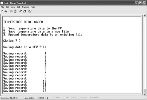
Figure 7.17 shows a screen snapshot where Option 1 is selected to read the temperature records from the SD card and display them on the PC screen.
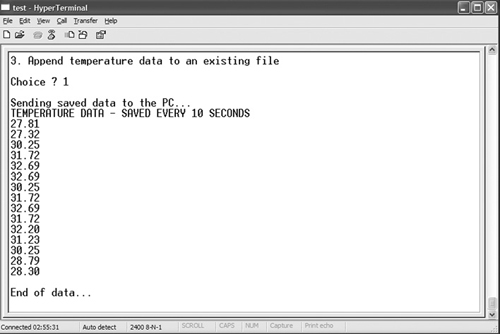
Finally, Figure 7.18 shows a screen snapshot when Option 3 is selected to append the temperature readings to the existing file.
