
Chapter 3. OpenCL Device Architectures
In this chapter, we discuss the design space of architectures in which OpenCL plays. We also discuss trade-offs in design that lead to different performance characteristics. Finally, we discuss specific architectures and examine where they fall in this space.
Keywords Architectures, cache, design, memory, register, SIMD, SMT, thread, VLIW
Introduction
OpenCL has been developed by a wide range of industry groups to satisfy the need to standardize on programming models that can achieve good or high performance across the range of devices available on the market. Each of these companies has specific goals in mind for OpenCL and targets for what features OpenCL should have to be able to run correctly on a specific architecture. To this end, OpenCL has a range of features that attempt to allow detection of unique hardware capabilities. For example, OpenCL has a relaxed consistency block-based parallelism model intended to run relatively efficiently on serial, symmetric multiprocessing (SMP), multithreaded, and single instruction multiple data (SIMD) or vector devices. In this chapter, we discuss some of these devices and the overall design space in which they sit.
Although OpenCL is designed to be a platform-independent applications programming interface (API), at the algorithm level and consequently at the level of kernel implementation, true platform independence in terms of performance is still a goal (versus a reality). As developers, we need to understand the potential advantages of different hardware features, the key runtime characteristics of these devices, and where these devices fit into the different classes of computer architectures. Once the reader is equipped with this deeper understanding of the targeted hardware, he or she can make informed choices when designing parallel algorithms and software. The reader should also better appreciate the philosophy behind OpenCL's design in terms of programming, memory, and runtime models.
Hardware trade-offs
Given the history of OpenCL and its early use for graphics APIs and pixel shaders, it is easy to understand how OpenCL has developed as a leading language targeted for GPU programming. OpenCL has become a popular programming API for the high-performance computing market. However, as the number of platforms supporting OpenCL grows (particularly in the embedded systems space), the overall impact of OpenCL should increase substantially.
What is not necessarily clear from this discussion is what a GPU really is and how it differs from these “other devices.” When we develop general-purpose code for a GPU, what makes the device still a “graphics processor?” Is this any more than the graphics-specific logic that the device still carries?
More questions arise when we try to think about this question in any detail. How many cores does a GPU have? To answer that question, we have to decide on a definition of “core.” What is a “many-core” device, and is it significantly different from a “multi-core” device? In general, different architectures choose different approaches to increase performance for a given power/transistor budget. Rather than simply being a raw compute power/electrical power/area trade-off, hardware developers have always also had to consider programming effort. The trade-off between these factors has created a wide divergence in designs.
Multi-core CPUs allow us to maintain the same frequency and complexity of control while adding more cores as transistor sizes reduce. With careful design, power consumption can be kept within reasonable limits. SIMD and very long instruction word (VLIW) architectures attempt to further increase the amount of useful work being performed by improving the ratio of arithmetic operations to control logic. In such cases, it can be difficult to generate workloads to keep the arithmetic logic units (ALUs) satisfied. Multithreading approaches this from a different angle. Rather than increasing the ratio of useful to computation to control logic, it increases the amount of useful work available to occupy computation logic to cover periods in which indirectly useful work is occupying noncompute logic such as memory pipelines. Thereby multithreading increases the utilization of the device we already have. Threading can be seen from the software side, in which case it can apply to multi-core chips as much as to single core designs, but it can also be viewed in terms of single cores managing multiple software threads. Caches and memory system trade-offs allow different architectures to target different data access patterns while trading off transistors for different uses.
In all these cases, we can apply the trade-offs to an individual core or a set of cores, depending on our definition of core. However, we do not need to apply the same trade-off across an entire device. Heterogeneity can enable hardware optimizations for multiple types of algorithm running simultaneously, giving better performance on both and hence overall. The traditional common example of this at the system level is the GPU + CPU combination we see in modern PCs (along with other lower performance processors scattered throughout the system). The latest generations of high-performance processors combine these two aspects into a single device, something that AMD calls the accelerated processing unit (APU).
In reality, we see combinations of these factors in different designs with different target markets, application, and price points. In this section, we examine some of these architectural features and discuss to what degree different common architectures apply them.
Performance Increase by Frequency, and Its Limitations
The easiest way, as a developer, to think about code we are writing is to create software that executes linearly: Perform one task, complete that task, perform another task. It is considerably more difficult for a developer to write parallel code, this is true even for limited SIMD or vector parallelism as is common in graphics. While multi-component pixels make this simple, in other applications extracting SIMD operations can be substantially more difficult. For this reason, architectures have historically aimed to increase the performance of a single thread of execution before moving to parallelism, with parallelism relegated to high-performance specialist machines in particular markets.
Shrinking of CMOS circuitry has allowed distances between transistors to scale fairly consistently for an extended period of time. The shrinking of distances and reduction in size of the capacitors allowed hardware architects to clock circuits at a higher rate. In turn, this led to Gordon Moore's famous self-fulfilling prophecy about transistor density and its misinterpretations into the realm of execution frequency and overall performance. Certainly, increasing frequency allowed the performance of nonparallel code to increase consistently during that time, such that it became an expectation for software developers until the early 21st century.
However, during the past decade, it has become obvious that continued scaling of clock frequencies of CPUs is not practical, largely due to power and heat dissipation constraints. The reason for this is that power consumption is dependent on frequency in a nonlinear manner. CMOS dynamic power consumption is approximated by the combination of dynamic and static power:
A is the activity factor, or fraction of the number of transistors in the circuit that are switching;
C is the capacitance of the circuit;
V is the voltage applied across the circuit;
F is the switching frequency; and
Ileak is an estimate of the current due to leakage of transistors.
It appears from this equation that power is linear with frequency. In reality, to increase the frequency, one has to increase the rate of flow of charge into and out of the capacitors in the circuit. This requires a comparable increase in voltage, which both scales the dynamic term and also increases the latter, static, term in the equation. For a long time, voltages could reduce with each process generation such that frequency scaling would not increase the power consumption uncontrollably. However, as process technology has reached the small sizes we see today, we can no longer scale the voltage down without increasing the error rate of transistor switching and hence frequency scaling requires voltage increases. The increase in power from any increase in frequency is then substantial.
As a second problem, increasing clock frequency on-chip requires either increasing off-chip memory bandwidth to provide data fast enough to not stall the linear workload running through the processor or increasing the amount of caching in the system.
If we are unable to continue increasing the frequency with the goal of obtaining higher performance, we require other solutions. The heart of any of these solutions is to increase the number of operations performed on a given clock cycle.
Superscalar Execution
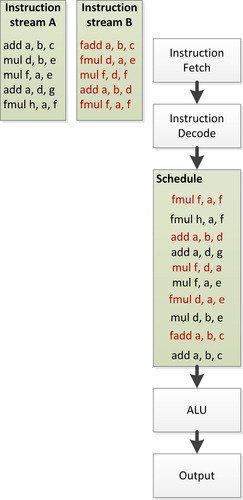
Superscalar and, by extension, out-of-order execution is one solution that has been included on CPUs for a long time; it has been included on x86 designs since the beginning of the Pentium era. In these designs, the CPU maintains dependence information between instructions in the instruction stream and schedules work onto unused functional units when possible. An example of this is shown in Figure 3.1.
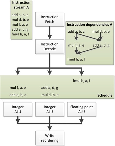 |
| Figure 3.1 |
The major advantage of out-of-order logic lies with the software developer. By extracting parallelism from the programmer's code automatically within the hardware, serial code performs faster without any extra developer effort. Indeed, superscalar designs predate frequency scaling limitations by a decade or more, even in popular mass-produced devices, as a way to increase overall performance superlinearly. However, it is not without its disadvantages.
Out-of-order scheduling logic requires a substantial area of the CPU die to maintain dependence information and queues of instructions to deal with dynamic schedules throughout the hardware. In addition, speculative instruction execution necessary to expand the window of out-of-order instructions to execute in parallel results in inefficient execution of throwaway work. As a result, out-of-order execution in a CPU has shown diminishing returns; the industry has taken other approaches to increasing performance as transistor size has decreased, even on the high-performance devices in which superscalar logic was formerly feasible. On embedded and special-purpose devices, extraction of parallelism from serial code has never been as much of a goal, and such designs have historically been less common in these areas.
Good examples of superscalar processors are numerous, from Seymour Cray's CDC 6600 to numerous RISC designs in the 1990s. Currently, high-end CPUs are mostly superscalar. Many GPUs also show superscalar capabilities.
VLIW
VLIW is a heavily compiler-dependent method for increasing instruction-level parallelism in a processor. Rather than depending entirely on complex out-of-order control logic that maintains dependences in hardware, as we saw when discussing superscalar execution, VLIW moves this dependence analysis work into the compiler. Instead of providing a scalar instruction stream, each issued instruction in a VLIW processor is a long instruction word comprising multiple instructions intended to be issued in parallel. This instruction will be mapped directly to the execution pipelines of the processor.
An example of VLIW execution is shown in Figure 3.2. This is the same set of instructions as we saw in Figure 3.1, but rather than being fetched serially, they are fetched in three horizontally arranged packets of up to three instructions. We now see that the dependence structure of this instruction stream is linear, and the hardware will treat it that way rather than extracting and tracking a more complicated dependence graph. The VLIW instruction packets are decoded, and each individual part of the instruction stream maps to a given computation unit in the processor for execution. In some VLIW designs, as in this example, the computation units are heterogeneous and hence some instructions will only ever be scheduled into a given lane of the VLIW packet stream. Other architectures present more homogeneous hardware such that any instruction can be issued in any location and only dependence information limits the possibilities.
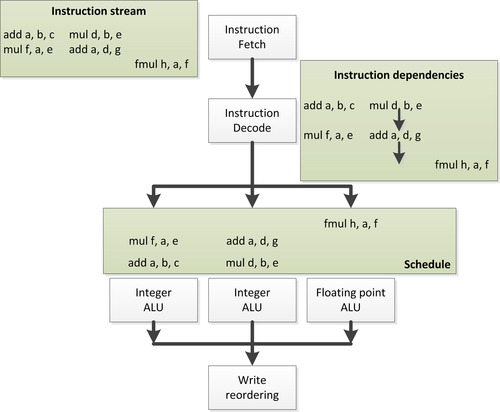 |
| Figure 3.2 VLIW execution based on the out-of-order diagram in Figure 3.1. |
In the example in Figure 3.2, we see that the instruction schedule has gaps: The first two VLIW packets are missing a third entry, and the third is missing its first and second entries. Obviously, the example is very simple, with few instructions to pack, but it is a common problem with VLIW architectures that efficiency can be lost due to the compiler's inability to fully fill packets. This can be due to limitations in the compiler or simply due to an inherent lack of parallelism in the instruction stream. In the latter case, the situation will be no worse than for out-of-order execution but more efficient as the scheduling hardware is reduced in complexity. The former case would end up as a trade-off between efficiency losses from unfilled execution slots and gains from reduced hardware control overhead. In addition, there is an extra cost in compiler development to take into account when performing a cost/benefit analysis for VLIW execution over hardware schedule superscalar execution.
SIMD and Vector Processing
SIMD and its generalization in vector parallelism approach improved efficiency from a slightly different angle compared with the former concepts. Whereas VLIW and hardware-managed superscalar both address extracting independent instruction parallelism from unrelated instructions in an instruction stream, SIMD and vector parallelism directly allow the hardware instructions to target data parallel execution.
Rather than specifying a scalar operation, a single SIMD instruction encapsulates a request that the same operation be performed on multiple data elements—conceptually a short vector operation. Vector computation generalizes this and usually works over long vectors, often pipelining computations over the data rather than executing on all elements simultaneously, and more generally supports gathered read and scattered write operation to and from memory.
If we again look at a variation on the running example as seen in Figure 3.3, we can see that the instruction stream is now issued linearly rather than out of order. However, each of these instructions now executes over a vector of four ALUs at the same time. The integer instructions issue one by one through the four-way integer vector ALU on the left, and the floating point instructions issue similarly through the four-way floating point ALU on the right. Note that although in this example we are issuing the instructions linearly, there is no reason to assume that we cannot perform these operations within a superscalar or VLIW pipeline, and we will see architectures that do just that in later discussion.
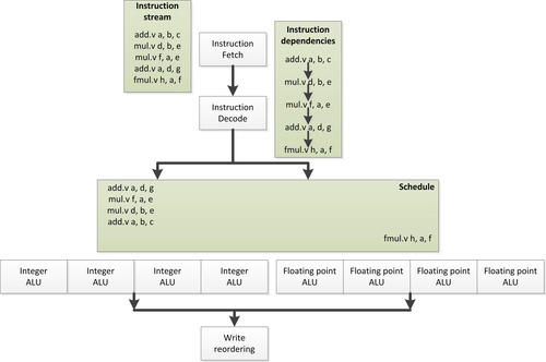 |
| Figure 3.3 |
The advantage of SIMD execution is that relative to ALU work, the amount of scheduling and instruction decode logic can both be decreased. We are now performing four operations with a single instruction and a single point in the dependence schedule.
Of course, as with the previous proposals, there are trade-offs. A significant amount of code is not data parallel, and hence it is not possible to find vector instructions to issue. In other cases, it is simply too difficult for the compiler to extract data parallelism from code. For example, vectorization of loops is an ongoing challenge, with little success in anything but the simplest cases. In these cases, we end up with unutilized ALUs and thus transistor wastage.
Vector processors originate in the supercomputer market, but SIMD designs are common in many market segments. CPUs often include SIMD pipelines with explicit SIMD instructions in a scalar instruction stream, including the various forms of Streaming SIMD Extension (SSE) and AVX on x86 chips, the AltiVec extensions for PowerPC, and ARM's NEON extensions. GPU architectures historically included explicit SIMD operations to support pixel vectors, and many modern GPUs also execute over wide implicit SIMD vectors, where the scalar instruction stream describes a single lane. Indeed, such machines can be considered vector machines because in many cases the vector is logical. For example, AMD's Radeon HD6970 architecture executes 64-wide SIMD operations, where each lane has a 128-bit vector register file. These wide vector instructions are pipelined over multiple cycles through a 16-lane SIMD unit.
Hardware Multithreading
The third common form of parallelism after instruction and data is thread parallelism, or the execution of multiple independent instruction streams. Clearly, this form is heavily used on large, parallel machines, but it is also useful within a single CPU core. As previously discussed, extracting independent instructions from an instruction stream is difficult, in terms of both hardware and compiler work, and it is sometimes impossible. Extracting such instruction parallelism from two independent threads is trivial because those threads already guarantee independence. The difficulty in terms of hardware shifts to managing the additional instruction stream and the state that a second instruction stream requires in terms of registers and cache.
There are two main ways to apply on-chip multithreading:
Simultaneous multithreading
Temporal multithreading
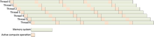
Simultaneous multithreading (SMT) is visualized in Figure 3.4. In this approach, instructions from multiple threads are interleaved on the execution resources by an extension to the superscalar scheduling logic that tracks both instruction dependencies and source threads. The goal is for the execution resources to be more effectively utilized, and in the figure that is the case. A higher proportion of execution slots are occupied with useful work. The cost of this approach is that the instruction dependence and scheduling logic becomes more complicated as it manages two distinct sets of dependencies, resources, and execution queues.
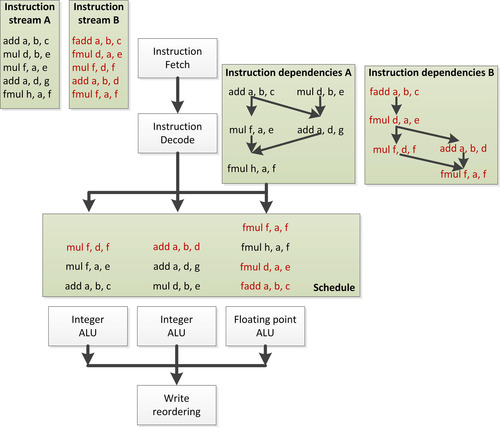 |
| Figure 3.4 The out-of-order schedule seen in Figure 3.1 combined with a second thread and executed simultaneously. |
Figure 3.5 shows the simpler time-sliced version of chip multithreading. In this case, each thread is executed in consecutive execution slots in round-robin fashion. For the purposes of simplification, the diagram shows a single shared ALU.
The following are advantages of this approach:
• The logic to handle the scheduling is simple.
• Pipeline latency can be covered by scheduling more threads, reducing the amount of forwarding logic.
This last case is the most useful in scaling to complicated problems. Many architectures are able to run more threads than necessary. When a thread reaches some sort of stall, it can be removed from the ready queue such that only threads in the ready queue are scheduled for execution. Once the stall ends, the thread can be placed back in the ready queue. In this manner, although a single thread might execute more slowly than on an out-of-order machine, the total throughput of the machine is kept high and utilization of compute resources can be maintained without overcomplicating the control logic. Taken to an extreme, this sort of heavy multithreading can be viewed as throughput computing: maximizing throughput at the possible expense of latency. The principle is shown in Figure 3.6.
 |
| Figure 3.6 |
Both forms of chip multithreading are common. The MTA design from Tera is a classic time-sliced multithreading supercomputer. The MTA design was difficult to manufacture; however, Cray's subsequent implementation, the MTA-2 design, utilized 128 register sets per CPU using fast thread switching between threads within this state and skipping stalled threads. The XMT design extends this further to fit multithreaded processors in standard AMD Opteron-based Cray systems. Sun's Niagara series of chips implements a multi-core multithreaded design (8 per core) to achieve low power and high throughput on data-center workloads. Intel's Pentium 4 and Nehalem/Sandy Bridge designs implement a form of SMT known as “hyperthreading.” Modern GPU designs runs numerous threads in a temporal fashion on each core, where the number is generally resource limited: On the current generation of AMD GPUs, this is usually 8–10 threads per core to cover latency and stalls.
Multi-Core Architectures
Conceptually at least, the simplest approach to increasing the amount of work performed per clock cycle is to simply clone a single core multiple times on the chip. In the simplest case, each of these cores executes largely independently, sharing data through the memory system, usually through a cache coherency protocol. This design is at its simplest a scaling down of traditional multisocket server SMP systems that have been used to increase performance for decades, in some cases to extreme degrees.
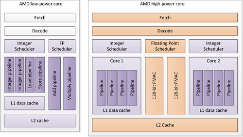
However, multi-core systems come in different guises, and it can be very difficult to define a core. For example, a mainstream CPU, at the high end, generally includes a wide range of functional blocks such that it is independent of other cores on the chip, barring interfacing logic, memory controllers, and so on that would be unlikely to count as cores. However, AMD's “Bulldozer” (high-power core) design shown alongside the simpler “Bobcat” (low-power core) design in Figure 3.7 shares functional units between pairs of cores in a replicable unit termed a module, in which a single thread will run on each core in a traditional fashion with the hardware interleaving floating point instructions onto the shared floating point pipelines. The aim of such a design is to raise efficiency by improving occupancy of functional units.
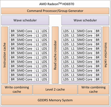
In a similar manner, GPU designs show a different definition of core. Modern GPUs have tens of cores—at the current high end, between 16 and 32 varying levels of complexity. However, if we look at the AMD Radeon HD 6970 high-level diagram shown in Figure 3.8, we see a similar approach to Bulldozer taken to an extreme. Although the device has 24 SIMD cores, by looking at the execution units in the fairest way to compare with traditional CPUs, those SIMD cores only execute ALU operations—both floating point and integer. Instruction scheduling, decode, and dispatch are executed by the wave scheduler units. The wave schedulers are so named because the unit of scheduling is a wide SIMD thread context known as a wavefront. Indeed, on the 6970, there are two of these to prevent overly high complexity, whereas lower capability parts in the series use only one and scale the number of SIMD cores. This is another example of efficiency by splitting into multiple cores. Memory operations on the 6970 are passed from the wave scheduler directly to the memory system without executing on the SIMD cores such that memory work is shared between cores much as the floating point units are shared on the Bulldozer design.
Integration: Systems-on-Chip and the APU
In the embedded space, a more heterogeneous approach to multi-core design is common. To achieve low power, embedded developers have constructed complicated systems-on-chip (SoCs) combining varied components into a compact and cost-effective design. Combining specialized components in this way allows devices to be optimized for a particular use case and power envelope, which is particularly important in markets such as the design of mobile phones.
Benefits from SoCs are the following:
• Combining multiple elements into a single device allows for a single manufacturing process and a single product to deal with, allowing for lower manufacturing costs.
• The smaller number of packages takes up less space in a final device, allowing for lower device cost and smaller form factor, which are vital in markets such as mobile telephony.
• Smaller distances mean less power used during communication and easier sharing of data through a single memory system.
Good examples of this approach in the mobile phone space are the Snapdragon SoC from Qualcomm and the OMAP series from Texas Instruments. Designs such as these combine an implementation of the ARM ISA, a mobile GPU, memory controllers, and various wireless and media processing components.
At the higher performance end of the market, Sony, Toshiba, and IBM developed the Cell Broadband engine processor that combines a number of small, high-performance but simple cores with a main traditional full-capability core with the aim of improving the performance/Watt characteristics. AMD and Intel have both developed combined CPU/GPU SoCs termed APUs by AMD, enabling high-performance graphics and CPU power in a more efficient single chip package.
Cache Hierarchies and Memory Systems
Whereas in the early years of supercomputers memory bandwidth and latency were such that CPUs could always access the data they needed when it was needed, it has been a long time since this has been the case. Currently, it is not unusual that the latency between a memory request on the CPU and the data being returned from memory is hundreds or even thousands of CPU cycles. On a single threaded CPU, out-of-order logic would be impossibly complicated to cover that much latency.
Fortunately, most applications do not make entirely independent memory accesses. In general, memory access patterns express some degree of locality, which will be either of the following:
• Spatial: Two or more memory accesses read or write addresses that are near each other, by some measure, in memory.
• Temporal: Two or more memory accesses read or write the same address (i.e., the same read is performed at different times).
Caches come in varied designs, but they can be divided into two general categories that are applied dependent on the workload. CPU caches tend to be designed to minimize latency. To achieve this, caches are large with complicated hierarchies to move as much of the data as close to the CPU core as possible. Out-of-order logic can only cover a limited amount of latency, so the fewer cycles to access data, the better. In addition, keeping data close to the execution units minimizes power consumption: Long-distance data movement is a significant component of CPU power usage.
Throughput processors are more latency tolerant, using threading to cover the cycles between request and data return. In these designs, the goal of caching is less to minimize latency, so the large multilevel hierarchy is less common, and more to reduce traffic across the limited memory buses. Smaller caches that allow neighboring accesses to be caught but are concerned less with very long periods of reuse are often seen in these situations, acting more as spatial filters. Wide SIMD units and programming models aim for efficient coalesced memory access to increase the size of memory transactions issues. The result is that dedicating logic to arithmetic units becomes a better use of transistors. In addition, higher latency, higher bandwidth memory interconnects allow this design to work more efficiently, although system-level issues such as pin availability and necessity to allow swapping of memory chips are equally important in this decision. One extension of this bias toward spatial locality that we often see in GPU design is to lay memory out such that two-dimensional accesses are efficiently cached.
Some designs including GPUs and the cell processor include software-managed scratchpad memory spaces as well as or in place of cache hierarchies. These buffers enable higher performance at a given power and area budget, but they require more complicated programming.
The reality of any given design is that it balances caching levels and features based on the expected workloads for the processor. Unfortunately, there is no right answer for all processor design/workload combinations.
The architectural design space
In the real world, we do not see many architectures that fit cleanly into just one of the previously mentioned categories. The reality is that computer architecture is a huge design space with enormous variation in all directions. Common current architectures sit in that design space at various points.
This is most important in helping us realize that some of the publicly held viewpoints of today's architectures can be overly simplistic. For example, in the domain of GPUs, we often encounter statements such as the following:
• CPUs are serial, GPUs are parallel.
• CPUs have a small number of cores, GPUs have hundreds.
• GPUs run thousands of threads, CPUs run one (or two).
The reality of any design is far more complicated than that, with wide variation in internal buffers, number of pipelines, type of pipelines, and so on. The theme of this chapter is to show that the difference between GPUs and CPUs, or indeed most modern architectures, is not fundamental. The majority of the visible architectural differences we commonly see today are simply points on a sliding scale, a set of parameterization knobs applied to basic designs. These are the differences the average programmer needs to understand: Only the expert need be concerned with ratios between buffer sizes and arranging instructions for hardware co-issue.
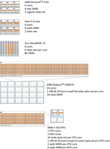
In this section, we discuss several real architectures and where they fit in the design space trading off some of the features we discussed previously. It is hoped that this will help to give a more nuanced feel for architectural trade-offs and help develop views on what algorithms may or may not work well on real architectures. Figure 3.9 gives a graphical hint toward some of the architectural trade-offs while ignoring caching to keep the diagram somewhat simple. In the design, we limit ourselves to extreme simplifications. The goal is to show that the wide SIMD and state storage design of GPUs is a long way along a spectrum from simple CPUs in terms of use of area, and that maximum performance and ease of achieving good performance depend on these design choices.
CPU Designs
The devices that most people are used to developing on can be loosely described as “CPUs.” Even within this space, there is considerable variation in how different forms of parallelism are utilized.
Low-Power CPUs
At the very lowest end of the power spectrum, CPU cores are very simple, in-order cores. At this level, power consumption is the most important factor in design, with performance a secondary consideration. Such designs often do not support floating point operations and have no need for parallelism.
Currently, the most widespread low-power CPU ISA is the ARM ISA developed in IP form by ARM Holdings. The ARM architecture originated in the Acorn RISC machine concept from Acorn Computers as a desktop architecture, but recently the simplicity of the architecture has made it dominant in the mobile and embedded markets, with a foray into Acorn's own desktop projects from 1996 to 1998 as the DEC-manufactured StrongARM. ARM designs come in a wide variety of forms because the ISA IP is licensed to manufacturers who are at liberty to design their own cores. Usually, ARM cores are combined within SoCs with other units such as cellular modems, embedded graphics processors, video accelerators, and similar devices.
Most variants on the ARM ISA have been in-order cores with three to seven pipeline stages. The Cortex-A8, -A9, and -A15 cores, based on the ARMv7 ISA, are superscalar and multi-core with up to four symmetric cores. The ARMv7-based cores may also support the Neon SIMD instructions, giving 64- and 128-bit SIMD operations in each core.
The AMD Bobcat CPU core that was shown in Figure 3.7 is the low-power core in AMD's current CPU lineup designed for a power range of 1–10 W. To achieve the low-power figures, Bobcat cores are clocked more slowly than the high-end parts as well as being carefully designed to reduce overhead—at the cost of lower peak performance. Bobcat is a 64-bit design, supports two-way out-of-order issue, and also has a 64-bit SIMD unit that can multicycle SSE operations.
Intel's Atom design takes a slightly different approach to performance compared with AMD's Bobcat. Atom does not support out-of-order execution, and as a result, single threaded performance suffers. However, Atom does support a form of temporal multithreading executing two threads at once. This allows Atom's performance on multithreaded workloads to be competitive in some circumstances.
In general, these low-power CPUs support in-order or narrow out-of-order execution with relatively narrow SIMD units. Variation in the number of cores can be used to scale to varied power/performance points in multithreaded situations. In all cases, these features are kept simple compared with desktop CPUs as a method for reducing power consumption.
Mainstream Desktop CPUs
Mainstream desktop CPUs from AMD and Intel do not look much different from the Bobcat design. In each case, they slightly increase the complexity of each element.
The AMD Phenom II represents AMD's current mainstream CPUs and is a constituent of the Llano APU that we discuss later. The Phenom II as sold has up to 6 cores (with the dual die Magny–Cours design having 12), allowing a high degree of parallel execution. The CPUs have large caches, up to 512 kB L2/core and 6MB L3 shared.
Each core carries a full 128-bit SSE unit that can issue add, multiply, and miscellaneous instructions simultaneously. It has a wide L1 cache interface (128 bits/cycle) and decodes, fetches, and issues six integer operations in parallel. Thus, the superscalar design has a wider capability than seen in the Bobcat core, which, along with increases in caches and branch predictor logic and a much higher clock frequency target, accounts for its higher performance, higher power consumption market segment.
Intel's Sandy Bridge microarchitecture occupies a similar market segment. Like Phenom, Sandy Bridge supports full 128-bit SSE operations through multiple pipelines and issues up to six operations of mixed types in parallel. In addition, Sandy Bridge supports 256-bit Advanced Vector Extensions (AVX) operations, allowing up to 16 single precision floating point operations per cycle. As with Atom, Intel added hardware multithreading support to Nehalem, Sandy Bridge's predecessor, and maintained this in Sandy Bridge. In this case, it is true SMT: Each core can mix operations from a pair of threads in the execution units. This increase in scheduling complexity is traded against the increased utilization of the functional units.
AMD's Bulldozer core, seen in Figure 3.7, increases parallel thread execution by taking a middle ground between increasing core count and increasing threads per core. Rather than increasing core count as in earlier AMD designs, which results in large per-core overhead, or using true SMT as in Sandy Bridge, with its high degree of scheduling complexity, Bulldozer takes a middle ground.
The approach used in Bulldozer is to create a second independent integer core with its own set of private ALUs, state and scheduler. However, the floating point ALUs are shared between pairs of cores, as are the fetch and decode blocks and the level 2 cache. The goal of this design is to only share functional units that are not likely to be overly heavily contended in real workloads.
Each core supports out-of-order execution through four ALU pipelines. The shared floating point ALU is a pair of 128-bit (SSE) SIMD units that can combine to execute AVX instructions. Bulldozer relies on multi-core execution to increase its thread count. However, each core is a relatively small area, so a higher core density should be possible compared with the Phenom design.
With mainstream CPUs, then, we see wide multi-issue out-of-order hardware, high clock speeds, and large caches—all features intended to maintain high single threaded performance with reasonably high power draw. In-core multithreading is kept minimal or nonexistent, and SIMD units are set at a width that does not waste too much area when not in use.
Intel Itanium 2
Intel's Itanium architecture and its more successful successor, the Itanium 2, represent an interesting attempt to make a mainstream server processor based on VLIW techniques. The Itanium architecture includes a large number of registers (128 integers and 128 floating points). It uses a VLIW approach known as EPIC, in which instructions are stored in 128-bit three-instruction bundles. The CPU fetches two bundles per cycle from L1 cache and hence executes six instructions per clock cycle. There are two 64-bit SIMD units on each core, and the processor is designed to be efficiently combined into multi-core and multi-socket servers.
The goal of EPIC is to move the problem of exploiting parallelism from runtime to compile time based. It does this by feeding back information from execution traces into the compiler. It is the task of the compiler to package instructions into the VLIW/EPIC packets, and as a result, performance on the architecture is highly dependent on compiler capability. To assist with this numerous masking, dependence flags between bundles, pre-fetch instructions, speculative loads, and rotating register files are built into the architecture. To improve the throughput of the processor, Itanium 2 implementations support two-way temporal multithreading, switching threads on certain events such as memory accesses that are likely to have long latency.
Niagara
The Niagara design (Figure 3.10), originally from Sun and under continuing development at Oracle, takes a throughput computing multithreaded approach to server workloads. Workloads on many servers, particularly transactional and web workloads, are often heavily multithreaded, with a large number of lightweight integer threads using the memory system. The Niagara, or UltraSPARC T series (with the T3 now just SPARC T3), is designed to efficiently execute a large number of such threads to maximize overall work throughput with minimal power consumption. Each of the cores is designed to be simple and efficient, with no complex out-of-order execution logic. Each core is designed to interleave operations from eight threads through two execution units. Figure 3.9 shows how much state is present compared with decode logic or ALUs, showing a clear preference for latency hiding and simplicity of logic compared with the mainstream x86 designs.
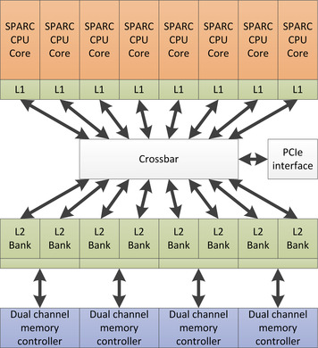 |
| Figure 3.10 Diagrammatic representation of the Niagara 2 CPU from Sun/Oracle. The design intends to make a high level of threading efficient: Note its relative similarity to the GPU design seen in Figure 3.8. Given enough threads, we can cover all memory access time with useful compute without extracting ILP through complicated hardware techniques. |
To support these threads, the design requires multiple sets of registers but as a trade-off requires less speculative register storage than a superscalar design. In addition, coprocessors allow acceleration of cryptographic operations, and an on-chip Ethernet controller improves network throughput. The UltraSPARC T2 (Grohoski, 2006) has 8 cores with eight threads each. The SPARC T3 expands this to 16 cores, with eight threads each.
GPU Architectures
Like CPUs, GPU architectures come in a wide variety of options. Here, we briefly discuss several before going into more depth about OpenCL programming for the AMD architecture. GPUs tend to be heavily multithreaded with sophisticated hardware task management because the graphics workloads they are designed to process consist of complex vertex, geometry, and pixel processing task graphs. These tasks and the pixels they process are highly parallel, which gives a substantial amount of independent work to process for devices with multiple cores and highly latency-tolerant multithreading. It is important to understand that barring sophisticated mechanisms to manage task queues, or to hide SIMD execution behind hardware management systems, GPUs are simply multithreaded processors with their parameterization aimed at processing large numbers of pixels very efficiently.
Handheld GPUs
Handheld GPUs have only recently started to gain general-purpose capabilities, with ARM and Imagination Technologies, in particular, discussing fully OpenCL-compliant IP to be released in the near future. At this scale, GPUs consist of a small number of cores, typically one to four, where each executes a large number of individual threads on a small pixel-size SIMD unit not entirely dissimilar to an SSE vector pipeline. For example, ARM's Mali-T604 architecture uses three types of computation pipeline in each of up to four cores. Intercore task management supports managing workloads across the cores: Much GPU threading in general is hardware controlled rather than exposed to the operating system. An embedded design such as the Mali-T604 can share the same global memory as embedded CPUs, reducing the need to copy data across memory spaces; in the ARM design, this data is fully cached.
At the High End: AMD Radeon HD6970 and NVIDIA GTX580
High-end desktop GPUs and their derivatives aim more for performance than maximal power efficiency. To achieve high memory bandwidth, a large number of pins are dedicated to memory traffic and GDDR5 memory is used to increase the per-pin memory bandwidth at the cost of higher latency. These devices use a mixture of features to improve compute throughput. These include wide SIMD arrays to maximize arithmetic throughput for a given number of issued instructions. The AMD Radeon HD6970 architecture seen in Figure 3.8 has 16 SIMD lanes in hardware and uses vector pipelining to execute a 64-long vector over four cycles. The NVIDIA GTX580 architecture (Figure 3.11) also uses a 16-wide SIMD unit and executes a 32-long vector over two cycles. Both devices are multithreaded, supporting numerous wide SIMD threads on each core. On the AMD architecture, for example, up to 32 active wide SIMD threads called wavefronts require state stored on the SIMD core (248 per wave scheduler), which can be selected from for execution on each cycle. In both cases, the number of wavefronts able to be active on a core depends on the resource constraints of the wavefronts in terms of register and local memory requirements. As a result, the effective number that can be active is lower than this, likely 4–8 wavefronts.
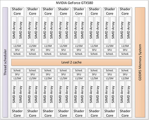
In both architectures, the intermediate language that programs the device is a lanewide SIMD model such that an instruction stream represents a single lane of the SIMD unit, so that each SIMD unit is visible, rather than vectorwide instructions as with x86 SSE or AVX instructions. Program counters are managed per SIMD vector such that a hardware thread is really a wide vector. The single-lane programs are grouped together using some degree of hardware vectorization, which allows efficient management of divergent branches, and stacks of masks to support predicated execution. To enable instruction-level parallelism, the AMD architectures use VLIW instruction streams in each lane extracted by the low-level shader compiler from the intermediate language. In the HD5xxx designs and most of the HD6xxx designs, this is a five-wide VLIW instruction, where all lanes are capable of most arithmetic instructions but the fifth is capable of specialized instructions such as efficient sine and cosine. In the Radeon HD6970 architecture, the VLIW is four-wide, with four identical VLIW lanes. The NVIDIA design in the GTX580 architecture achieves instruction-level parallelism by co-issuing two threads at once over two execution pipelines. Both designs are superscalar in that execution resources can issue memory access, arithmetic, and other operations from threads running on the same core, if not necessarily from the same thread.
Like the mobile GPUs on the market, the high-end AMD and NVIDIA models comprise multiple cores. Defining a core as the closest reasonable mapping to the equivalent in a CPU architecture, the AMD design has 24 cores and the NVIDIA design has 16.
Each of these cores includes a scratchpad memory buffer, which takes area on the chip and as a result is excluded from many handheld designs. This scratchpad memory, known as local data share on the AMD architecture, is used to store the OpenCL local memory structures. Local memory is allocated per workgroup and fixed for the execution of those groups, so this physical structure limits the amount of concurrency if each workgroup uses a significant amount of local allocation. This memory is directly mapped to each executing group, is very fast, and consumes relatively little power compared with hardware-managed caches.
The Radeon HD6970 example in Figure 3.9 shows just how much register state GPUs support in comparison with CPU designs: There are many threads (eight in the diagram, which is typical), each of which is 64 wide on the AMD architecture.
APU and APU-Like Designs
SoCs have been common in embedded markets for a long time. Currently, there is a move toward SoCs being used for much higher performance systems and applications. Such fused processors, most obviously combining CPU and GPU designs, begin to encroach on the netbook, notebook, and low-end desktop spaces. It is easy to imagine such designs moving into high-end desktops. In this space we might see the power saving capabilities of integration combined with the substantial compute capability of a discrete GPU.
Currently, the three major architectures in this market are AMD's Bobcat-based and Phenom II-based Fusion products (Advanced Micro Devices, 2011) and Intel's Sandy Bridge range.
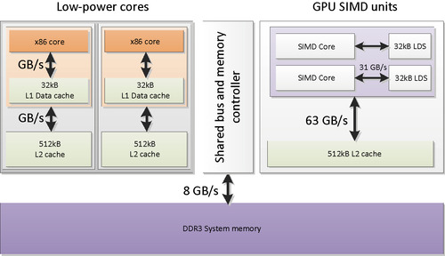
The AMD designs targeted at low-end netbook and subnotebook machines with a 9–18 W power budget are known as Ontario or Zacate and are based on the low-power Bobcat CPU core combined with a low-end GPU. These components are produced together on a single silicon die on a 40-nm process. The highest spec model in the range is shown in Figure 3.12. In this case, the GPU is an eight-wide SIMD unit based on the five-way VLIW of the 5xxx GPU generation from which the architecture is derived. The two Bobcat cores have two-way SIMD units, each allowing SSE instructions to be issued from each core over two cycles. AMD's higher performance APU, Llano, is based on the Phenom II core and a significantly higher performance GPU.
 |
| Figure 3.12 |
Intel's Sandy bridge APU design (Figure 3.13) is based on four cores of the Sandy Bridge CPU core discussed previously. The GPU is part of the ongoing development of Intel's in-house embedded GPU design, which currently does not support OpenCL but does enable the efficient graphics support expected from these fused processor architectures.
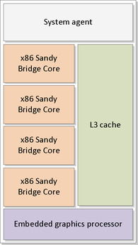 |
| Figure 3.13 |
The APU architectures offer scope for sharing data structures between GPU and CPU cores such that the major communication bottleneck of many GPU compute workloads is alleviated. This means that latency can be improved for workloads dispatched to the GPU and more tightly integrated algorithms between GPU and CPU cores can be created that are currently not practical due to performance constraints arising from the latency of the PCI express bus. This improvement comes at the cost of CPU-style memory bandwidth shared between both devices, losing the very high-bandwidth exotic memory interfaces of discrete GPUs. It is likely that this trade-off is advantageous in the wide range of algorithms that are inefficient when implemented purely on the GPU, due to the GPU throughput-based design being suboptimal for serial code, and in those algorithms in which communication is the performance bottleneck.
Summary
In this chapter, we discussed the types of architecture that OpenCL might run on and the trade-offs in the architectural design space that these architectures embody. After examining OpenCL more closely, in Chapter 6 we discuss how the OpenCL model maps to a specific architecture in the form of a combination of AMD Phenom II CPU and HD6970 GPU.
The content of this chapter will benefit from further reading; however, for many of the specific devices, concise references can be difficult to find. The fourth edition of Computer Organization and Design (Patterson and Hennessy, 2008) discusses many architectural issues in-depth, including the AMD Opteron, Intel Nehalem (predecessor to Sandy Bridge, sharing many features), UltraSPARC T2, and various other designs. It also contains a section on NVIDIA's GPU architecture. The fifth edition of Computer Architecture (Hennessy and Patterson, 2011) extends these concepts. NVIDIA released a white paper on its Fermi architecture in 2009 (NVIDIA, 2009). Chapter 2 of the Itanium 2 processor manual (Intel, 2002) gives a reasonably high-level overview of the EPIC implementation and processor pipeline.
References
Advanced Micro Devices, Incorporated, AMD Fusion Family of APUs: Enabling a Superior, Immersive PC Experience. (2011) Advanced Micro Devices, Incorporated, Sunnyvale, CA.
Grohoski, G., Niagara-2: A Highly Threaded Server-on-a-Chip. (2006) ; 18th Hot Chips Symposium, August.
Hennessy, J.L.; Patterson, D.A., Computer Architecture: A Quantitative Approach. 5th ed. (2011) Morgan Kaufmann, Burlington, MA.
Intel Corporation, Intel Itanium 2 Processor: Hardware Developer's Manual. (2002) Intel Corporation, Santa Clara, CA.
NVIDIA Corporation, NVIDIA's Next Generation CUDA Compute Architecture: Fermi. (2009) NVIDIA Corporation, Santa Clara, CA.
Patterson, D.A.; Hennessy, J.L., Computer Organization and Design. 4th ed. (2008) Morgan Kaufmann, Burlington, MA.
..................Content has been hidden....................
You can't read the all page of ebook, please click here login for view all page.