
4
Internal Antenna
The internal antenna emerged around the end of the twentieth century and gained its popularity in merely a few years. Nokia was the first mainstream cell phone company who successfully marketed phones with internal antennas. As shown in Figure 4.1, the Nokia 3210, which came onto the market in 1999, was a huge hit and more than 300 million of them were eventually sold around the world. “Candy‐bar phones,” a nickname for those phones with internal antennas strongly resonates with the European fashion taste, which appreciates minimalism and sleek curves. With that momentum, Nokia successfully eroded Motorola’s market share in Europe.

Figure 4.1 Nokia 3210.
(Source: Reproduced with permission of Nokia.)
After that, there were a few years of de facto draw between Nokia and Motorola, who shared the first and second places on the global chart of cell phone sales. Nokia claimed that it sold the most phones and Motorola insisted that its revenue of cell phones was the highest. Both claims were correct, because Motorola was still holding onto the high‐end market. What happened next was quite theatrical. Nokia wanted to use only candy‐bar phones to conquer the US market but kept failing. US customers didn’t want to give up their love of flip phones, which had been invented by Motorola. Nokia did not want to develop flip phones and hoped, through advertising and customer education, that Americans’ attitude toward candy‐bar phones could be converted in a relatively short period. Sadly, history demonstrates again how strong the persistence of people’s habits is.
Nokia’s love of internal antenna is not really emotional; it is because there are some technical and financial merits inherent in internal antennas. A candy‐bar phone with an internal antenna has no moving parts and only one printed circuit board (PCB). A handful of screws can securely assemble all the core parts. The front and back covers, which are made of acrylonitrile butadiene styrene (ABS plastic), are snapped onto the core without any screws. When a candy‐bar phone is accidentally dropped on the ground, the covers take most of the force. Because there are no screws attached to the covers, there is no extreme stress point. When the force is too strong to bear, the snap feature just breaks loose and absorbs all energy in the process. After the drop, a candy‐bar phone might fall apart; however, nothing is really broken; one can put it all back together and the phone is ready to work again. The robustness of a candy‐bar phone is one of critical factors that made Nokia so successful in the markets of the developing countries. Due to the cut‐throat competition, the margin of low‐tier phones is razor thin, and an increase of field failure rate (FFR) by a small percentage might totally wipe out the profits.
Unlike flip phones, candy‐bar phones do not have features such as flip, hinge, board‐to‐board connector, and so on; the shorter build of material (BOM) of candy‐bar phones also means less manufacturing cost. Combining the cost‐saving on the stages of both manufacturing and customer service, Nokia can sell a low‐tier phone at a price which is lower than Motorola’s cost and still make decent money. For Nokia, moving into the field of flip phones with external antennas meant fighting a war in its enemy’s territory while losing most of its competitive advantage. Nokia’s own wishful thinking was that it could corner Motorola in the US market with candy‐bar phones with internal antennas combined with a price war, but apparently this didn’t work.
On the other hand, Motorola did not want to fight in the field of candy‐bar phones either. The reason for that is because of Nokia’s fearful logistic capability and its sophisticated global sourcing system. For most components used in Nokia, there is more than one vendor in the supplier pool. By doing this, Nokia can hammer vendors and demand a lower price and mitigate the possible part shortage due to any single vendor’s failure. In the meantime, the possible vendor of any component in the supplier pool is limited to a handful. There is a strict process in place to qualify a potential vendor, only heavyweight players in the according discipline have the possibility of being qualified. The strict screening process ensures the quality of parts used in phones, thus assuring the reliability in phone manufacturing. All these issues might sound quite simple, but in fact it is quite a challenge to implement them successfully.
Finally, both sides moved into their counterpart’s territory. It was a fierce fight, which eventually expanded to new fields with the emergence of new form of factors, such as slide phones and swivel phones. It now all seems a distant history. When the first version of this book was written, in 2009, Nokia claimed more than 40% of the global phone market and Motorola’s market share was wandering in the territory of single digit. With the blow of the ongoing economic crisis, which was the worst since the 1930s, Motorola’s fate did not look bright.
When the second version of this book was written, in 2015, a lot has happened. The mobile division of Motorola had been sold to Google for $12.5 billion in 2012. Google then resold the Motorola Mobility to Lenovo for $2.91 billion in 2014. Google still retains ownership of the vast majority of Motorola Mobility’s patents. Nokia Mobile’s market share had collapsed from the above 40% in 2009 to less than 10% in 2012. Microsoft bought Nokia Mobile in 2013 for $7.2 billion. Microsoft failed to turn around Nokia Mobile and layoff off 12,500 previous Nokia’s employees in 2014.
The disruptive force behind all that has happened is Apple. In 1997, everything seemed against Apple, the inventor of the personal computer, and bankruptcy seemed its only fate. Then suddenly, with the return of the expelled founder Steve Jobs, everything turned around. The first iPhone, iPhone 2G, was released in 2007 and sold more than 10 million in the next year. In 2011, Apple sold 71 million iPhone and Steve Jobs passed away in the same year. Many people were wondering whether Apple might lose its direction and luckily it didn’t. Apple has sold 169 million iPhone in 2014. Since iPhone 2G, every generation of iPhones adopted internal antennas. Although Google has failed to revive Motorola Mobile, Google’s phone operation system, Android, has dominated smartphone market. Except iPhone, which uses its own iOS system, everyone else pretty much all use Android. In 2015, the first‐tier smartphone vendors are Apple and Samsung, each claims around 20% worldwide market share. Three Chinese companies, Lenovo, Huawei, and Xiaomi, are distant followers. Each takes around 5–6% market share. In 2015, all phone models released by those companies use internal antennas.
Although to a customer, all internal antennas might have the same appearance, that is, no visible evidence of an antenna’s existence, there is more than one kind of internal antennas if we categorize them from a technical point of view. We are going to discuss some of them in this chapter. The aim of the book is to introduce the world of antenna designing. With the knowledge shared in the book, one should be able to design an antenna for most applications. In some tightly constrained applications, such as designing a multiband antenna in a tiny volume, the antennas introduced here may not be enough to fulfill the requirements. In those circumstances, a book by Professor Wong [1], Planar Antennas for Wireless Communications, provides more advanced techniques to meet such challenges.
4.1 Inverted‐F Antenna
Let’s start with the inverted‐F antenna (IFA). We know that a monopole antenna works pretty well for mobile applications. However, the size of a monopole is too big to be adopted in most state‐of‐the‐art phones. Naturally, L‐shaped antennas as shown in Figure 4.2 were proposed as a measure to decrease the total height of an antenna.

Figure 4.2 L‐shaped antenna.
While keeping the total antenna’s length, say, 70 mm, the antenna whip can be bent into an L shape in different positions, thus providing a different separation, G, from the ground plane. The dimension G is a critical parameter which decides the antenna’s impedance. Shown in Figure 4.3 are simulated results of a straight whip antenna and two L‐shaped antennas. When the horizontal arm approaches the ground plane, the real part of the antenna’s impedance becomes smaller. That means the impedance locus sweeps a larger circle on the Smith chart. As the impedance of a straight whip is around 100 Ω, when the whip is bent and approaching the ground, the matching of the antenna is actually improved at first. In this example, the antenna with the G equaling 14 mm is the best matched one of all three. However, if the separation between whip and ground is less than 14 mm, the matching starts to degrade.

Figure 4.3 Impact of separation G on an L‐shaped antenna.
Using the matching techniques discussed in Chapter 2, good matching can be easily achieved. Either a shunt inductor or a shunt capacitor can be used to match the antenna. Shown in Figure 4.4 are simulated results. A lumped inductor is used to match the antenna with G = 6 mm. The dashed line, solid line, and dotted line correspond to three different matching values. For a shunt inductor, a smaller value has more impact on the port impedance. A 6.8 nH inductor provides the best matching.

Figure 4.4 Using a shunt inductor to match the antenna with G = 6 mm.
By replacing the lumped inductor with a grounding metal strip, what we get is an IFA as shown in Figure 4.5. The shape of the antenna element is like the letter “F” on its side; that is why it is called “inverted F.” Shown in Figure 4.6 are the results of two IFAs. For the sake of consistency, the total whip length of both antennas is kept to 70 mm if measured from the feeding point to the end of the whip. The separations between the feeding and grounding strips are chosen to be 2 and 5 mm, respectively. Comparing Figures 4.4 and 4.6, it is clear that the grounding strip indeed functions as a shunt inductor. As the inductance of the grounding strip is decided by its total length, when the separation between the feeding and grounding strips becomes shorter, the distributed inductance become smaller, thus the grounding strip has more impact.

Figure 4.5 Inverted‐F antenna (IFA).

Figure 4.6 Impact of separation S on an IFA.
As a rule of thumb, whenever the separation between the arm of an IFA and ground gets smaller, the grounding strip must be placed closer to the feeding strip to compensate for the impedance change.
In practice, designing a single‐band IFA is quite easy. The following are some design steps:
- Start with a strip a little longer than a quarter of wavelength. A 4 mm gap between grounding and feeding strips can be used as the starting point.
- Tune the antenna length to get a resonance, which is slightly lower than the target frequency.
- Check the impedance on the Smith chart. The impedance must look similar to one of the three curves shown in Figure 4.4. If it resembles the dashed line, increase the gap S. If it resembles the dotted line, decrease S. The solid line is the preferred option.
- Fine‐tune the antenna length again until the correct resonant frequency is obtained.
Looking at Figures 4.4 and 4.6 more closely, the difference between resonant frequencies can be observed. When the antenna lengths are identical, an L‐shaped antenna can work at a lower frequency. To qualitatively explain this, a simplified equivalent circuit of an IFA is given in Figure 4.7. Unlike an L‐shaped antenna, whose resonant frequency is decided by its whole whip, only a part of IFA, which is marked by the dark color in Figure 4.7, is the active element. The effect of grounding and feeding strips can be approximated by a shunt inductor and a series inductor, respectively. Of course, this is only a coarse simplification, when the distance between feeding and grounding strip become too short, the distributed shunt capacitance between two strips can also play a role in the antenna performance.

Figure 4.7 Simplified equivalent circuit of an IFA.
As we know that E fields excited by a whip antenna are always parallel to the whip itself as shown in Figure 4.8a, one might assume that the E field generated by an IFA should rotate 90°, as the whip is rotated 90°. In fact, the rotation of an IFA’s whip has little impact on the polarization of radiation pattern. Similar to monopole antennas, an IFA cannot work by itself. It must be installed on a ground and it is the ground that decides the E‐field polarization. As shown in Figure 4.8b, when the ground is vertically placed, the E field is also vertically polarized.

Figure 4.8 E field excited by antennas.
Shown in Figure 4.9 are simulated three‐dimensional (3D) radiation patterns of an IFA. The antenna is the same one simulated in Figure 4.6 with S = 5 mm. Shown in Figure 4.9a is the 3D pattern of Eθ, which is the vertical polarization part of total E field. Figure 4.9b is the Eφ, the horizontal part of the total E field. The amplitude unit used in both plots is dB. The scale they used is also the same. It is clear that the vertical E field is the dominant radiation component. The peak gain of the vertical E field is 3.4 dBi. That of the horizontal E field is only −5.8 dBi. At a low frequency, such as 1.05 GHz, the radiation pattern of the ground is similar to a dipole, which is donut‐shaped and approximately omnidirectional in the azimuth plane. At a higher frequency, because the ground is much larger than one wavelength, the radiation pattern will split. This behavior is similar to that of a monopole antenna. Detailed studies of the ground effect can be found in Section 3.4 and published papers [2–5].

Figure 4.9 Three‐dimensional radiation patterns, IFA, S = 5 mm, 1.05 GHz.
An IFA does not provide a lot of design freedom, so it is mostly used in single‐band applications, such as GPS, BT, or WiFi. Although an IFA is similar to an L antenna with a shunt matching inductor, there is a minor difference. Because the active length of an L antenna starts from the feeding point, it can be designed to be smaller than an IFA. An L antenna also requires a smaller area on the PCB, because it only needs one contact pad. The drawback of an L antenna is that the lumped matching inductor it requires has some inherent losses, thus the efficiency of an L antenna is normally a few tenths of dB lower than an IFA’s. If there is enough board area for two pads, one for grounding and one for feeding, an IFA is a better choice, as it provides better efficiency and also saves a matching component, which costs a few pennies.
4.2 Planar IFA
4.2.1 Single‐Band PIFA
Shown in Figure 4.10 is a planar IFA (PIFA). PIFAs can be thought of as a mutation of IFAs. Both IFA and PIFA have a ground strip and a feeding strip. By replacing the radiating strip of an IFA with a patch, we get a PIFA. In most cases, the patch of a PIFA is above the ground plane.

Figure 4.10 Planar inverted‐F antenna (PIFA).
In all the following samples in this section, the width of both feeding and grounding strip is 1 mm; the dimension of PCB, which is used as the ground, is 50 mm × 120 mm. If the PCB size is changed, the antenna response will change accordingly. The ground’s impact on a PIFA is the same as that on an external antenna. Refer to Section 3.4 for further details.
In Figure 4.10, the dimension H is the distance between a patch and a ground. The S is the edge‐to‐edge distance between feeding and grounding strips. Similar to IFAs, the matching of antennas can be tuned by adjusting S.
Let’s start with single‐band PIFAs. Shown in Figure 4.11 are simulated results of three PIFAs. The dimension L of all three antennas is 50 mm, which is the same as the PCB width. The dimension W of three antennas is 5, 15, and 25 mm, respectively. To best match individual antennas, the dimension S, the distance between feeding and ground strips, is tuned case by case. The optimal S for 5, 15, and 25 mm patches are 1.5, 4, and 4 mm, respectively. When the W is 5 mm, the antenna is more like an IFA than a PIFA. With the increase in W, the resonant frequency of a PIFA decreases. This phenomenon gives us a hint that, unlike an IFA, the resonant frequency of a PIFA is not solely decided by the patch’s length.

Figure 4.11 Three PIFAs with different widths H = 7 mm.
For a PIFA, the resonant frequency is proportional to the summary of its length and width. As shown in Figure 4.12, a PIFA’s width plus its length is roughly a quarter of a wavelength at its resonant frequency.

Figure 4.12 Estimating the resonant frequency of a PIFA.
When discussing a single‐band PIFA, most books prefer to give a current distribution which shows two clear current flows. Both of them start from the upper‐left corner and end at the bottom‐right corner. One of them passes the bottom‐left corner and the other one passes the opposite top‐right corner. That is a quite intuitive but coarse simplification. The real current distribution is a little more complex than that. In many cases, it is difficult to see a clear current pattern when you simulate a PIFA.
Shown in Table 4.1 is a comparison between three antennas. The second column in Table 4.1 is the calculated resonant frequencies based on the assumption that W + L equals to a quarter of wavelength. The third column is the actual frequency. The fourth column is the ratio between the calculated frequencies and the actual ones. The actual resonant frequency of a patch is normally lower than the theoretical one. That is due to the loading effect of the edge capacitance between patch and ground.
Table 4.1 Accuracy of simplified frequency calculation formula
| Calculated frequency (GHz) λ/4 = (W + L) | Actual frequency (GHz) | Actual frequency/calculated frequency | |
| W = 5 mm, L = 50 mm | 1.36 | 1.26 | 0.92 |
| W = 15 mm, L = 50 mm | 1.15 | 1.12 | 0.97 |
| W = 25 mm, L = 50 mm | 1.00 | 0.89 | 0.89 |
The critical parameter, which controls the bandwidth of a PIFA, is H, the distance between a patch and a ground. Shown in Figure 4.13 are the reflection coefficients of three antennas with different heights. All patches have the same L and W, which are 50 and 25 mm, respectively. The H of three patches is 5, 7, and 9 mm, respectively. All three antennas are individually tuned, their S are 3, 4, and 7 mm accordingly. By increasing the H from 5 to 9 mm, an antenna’s −10 dB bandwidth is almost tripled.

Figure 4.13 PIFA’s bandwidth vs. height. L = 50 mm, W = 25 mm.
As a summary, there are three design guidelines for single‐band PIFA:
- The dimension H is the most critical parameter which decides an antenna’s overall performance. However, because H is directly related to a device’s thickness, it is a tough task to bargain about it with industry design engineers or mechanical engineers. If there is only a 5 mm height clearance and a quad‐band GSM antenna is required, then PIFA is not an appropriate candidate. A folded monopole antenna, discussed in Section 4.3, is a better choice.
- By adjusting the total length W + L, the antenna’s working frequency can be tuned. In practice, the L should be similar to the PCB’s width that results in wider bandwidth.
- The dimension S is the tuning parameter which optimizes an antenna’s matching. One can either use a wider strip with a larger S or a narrower strip with a smaller S to achieve the same matching. A larger S is better for manufacturing, because a fixed process tolerance causes less electrical variance in the antenna. From a mechanical point of view, a narrower strip is better for spring finger type of designs, because it is more flexible and it is easier to achieve the required spring force.
4.2.2 Multiband PIFA Antenna with Slits
If you have already discovered PIFAs, then you might find that the following explanation is somewhat different from other books. All versions of PIFA explanations are partially correct, including the following version. As a PIFA is a distributed radiating system, too many parameters play a role in deciding the antenna’s characteristic. To explain such a complex matter, one has to substantially simplify it and that is the reason for the different explanations.
There are several ways to design a multiband PIFA. The most popular way is to cut slits on the patch, as shown in Figure 4.14. Similar to a single‐band PIFA, a dual‐band PIFA also has a grounding strip and a feeding strip. Two critical dimensions, D and C, are used here to describe the slit. The dimension D is the distance between the patch’s corner and the opening of the slit. The dimension C is the slit’s length. The dimension P is the distance between the horizontal part of slit and the edge of patch. The P is not really a critical dimension; however, it decides the shape of the slit.

Figure 4.14 Dual‐band PIFA.
Shown in Figure 4.15 are the decisive paths of different bands. Figure 4.15 only serves the purpose of predicting the trends of frequency shifting when different dimensions are adjusted. One should not try to use the illustrated critical path shown in Figure 4.15 as a way of calculating a patch’s resonant frequency. In reality, trying to predict a patch’s resonant frequency with a calculator is not really an efficient design approach. There are always so many unknown parameters, such as the permittivity of both the antenna support and the phone cover, the electrical property of nearby objects, and so on. Usually, all these unknowns can make the theoretical calculation far removed from the correct answer. A better approach is to memorize the effect of each parameter first, then make a PIFA with a piece of copper tape, install it on a mock‐up phone, cut a slit on the PIFA, and tune it by trial and error.

Figure 4.15 Decisive paths of different bands.
The impacts of the two critical dimensions are listed below:
- The distance D can affect the resonant frequency of both the lower and the higher bands. It always shifts two bands in the opposite directions. For example, if we decrease D, the critical path of the lower band will be shorter, thus increasing its resonant frequency. In the meantime, the critical path of the higher band is increased, thus inducing a lower resonant frequency.
- The slit’s length C only influences the higher band. The slit is about half the total critical path of the higher band. Increase C can lower the high band.
Of course, in the real world, the effect of any dimension change cannot be exclusively constrained in a single band. In fact, it is safer to claim that it has more impact on some bands than others. To help understand the design rules, the following design examples are provided. In all the following examples, the area of patch is 50 mm × 25 mm; the area of ground is 120 mm × 50 mm. H, which is the distance between ground and patch as shown in Figure 4.10, is 7 mm. The impact of D is illustrated in Figure 4.16. By adjusting D, both low and high resonant frequencies can be tuned simultaneously and in opposite directions.

Figure 4.16 Impact of dimension D. 50 mm × 25 mm Patch, P = 15 mm, C = 40 mm.
Illustrated in Figure 4.17 are the impacts of slot length C. With the increase of a slot’s length, the resonant frequency of the higher band decreases. It can be seen that the resonant frequency at the lower band still drifts a little bit. For all three cases shown in Figure 4.17, the dimension P is fixed, the modification of C is realized by only increasing or decreasing the length of the horizontal portion of the slit.

Figure 4.17 Impact of dimension C. 50 mm × 25 mm Patch, P = 15 mm, D = 10 mm.
Shown in Figure 4.18 are the results when the dimension P is changed while keeping the slit length C fixed. Although not significantly, the dimension P also has some impact on the higher band. It can be used in some circumstance as a means to provide the “extra mile” for tuning.

Figure 4.18 Impact of dimension P. 50 mm × 25 mm Patch, C = 35 mm, D = 10 mm.
Shown in Figure 4.19 are the radiation patterns of a PIFA. At the low band, which is 0.78 GHz in this case, the radiation pattern is similar to a dipole’s. The radiation is mostly generated by the vertical current along the edge of the ground plane. The vertical polarized field Eθ is the dominant field component. At the higher band, which is 1.75 GHz, the amplitudes of Eθ and Eφ are in the same order of magnitude. Shown in Figure 4.19e is the radiation pattern of the total E field at 1.75 GHz. It confirms again that it is the ground plane, instead of the antenna element itself, which definitively decides the radiation patterns.

Figure 4.19 Radiation patterns of PIFA, P = 15 mm, D = 15 mm, C = 40 mm.
When designing any kind of antenna, antenna engineers may find themselves in a situation where one band has more than enough bandwidth but the other band cannot meet the specification. Knowing how to exchange bandwidth between bands is an essential technique. For a PIFA, cutting the slit shape differently can have some effect on the bandwidth ratio between bands. The other way to change the ratio is by adjusting the slit’s width. Shown in Figure 4.20 are the simulated results of three PIFAs with the same dimensions but different slit widths. With the decrease in the slit’s width, the bandwidth increases at the lower band and decreases at the higher band.

Figure 4.20 Bandwidth trade‐off between low and high bands.
If an antenna still cannot meet the specification after the performance of both bands have been balanced, the only way out is to attempt to increase the patch’s height, which is the dimension H shown in Figure 4.10a. This definitely is an uphill battle.
So far, we have shown how to adjust both bands simultaneously or modify the high band independently. By combining both methods, we can tune the resonances freely in a quite wide range. Now let’s discuss some matching techniques. The easiest way to match an antenna is to design a matching circuit. However, a matching circuit always has some inherent loss. For a patch antenna, some of the dimensions can be modified, so we should always try to achieve a good match by tweaking the patch itself first. By comparing Figures 4.16 and 4.17, we can see that there are different ways to cut the slit to achieve two required resonant frequencies, and their matching conditions are also different.
Besides the patch itself, another useful tuning mechanism is the feeding and grounding structure. Shown in Figure 4.21 is the equivalent circuit of feeding and grounding strips. The grounding strip is equivalent to a shunt inductor, so it has more impact on the lower band. The feeding strip is equivalent to a series inductor, and it can be used to tune the high band. To increase the inductance of grounding strip, the following methods can be used:
- Increase the length of grounding strip by bending the strip.
- Decrease the width of grounding strip, t2.
- Increase the distance between feeding strip and grounding strip, S.

Figure 4.21 Equivalent circuit of feeding and grounding strips.
Similarly, the inductance of feeding strip can also be increased by increasing the length or decreasing the width of the strip. Shown in Figure 4.22 are two other ways of matching. Figure 4.22a shows how to use the slit to increase the shunt inductance. Figure 4.22b shows how to add some distributed shunt capacitance. Another effect of the stub shown in Figure 4.22b is to increase the total current length, thus decreasing the overall resonant frequency. If you have a brainstorming session on this topic, lots of matching structures can be invented. Where should we stop and hand over the remaining tasks to lumped matching element? There is no right or wrong answer to this question. Normally, it is a purely personal choice. Some engineers prefer a self‐matched design without requiring any lumped components. Many of those engineers treat antenna design as an art. Some engineers like to reuse previous designs and want to push dimension changes to the minimum. For them, a matching circuit is the favorite choice.

Figure 4.22 Other ways of matching.
Putting the personal preference aside, there are some objective criteria that can be used to evaluate any antenna design. How sensitive is a design to manufacturing tolerance? What kind of manufacturing process can it use? Is a design easy to be tuned when frequency drifts? Does frequency tuning require expensive and time‐consuming tooling modifications? What is the efficiency of an antenna?
It is not difficult to imagine that the weight of each criterion varies from project to project. For a low‐end phone, cost might be the first consideration. For a high‐end phone, it is most likely that all physical constraints have been pushed to the limit; the only goal for an antenna engineer is to meet the specification at any cost. The duration of a project is also an important factor when selecting different approaches. In fact, most issues mentioned here are not academic at all, they are purely practical matters. Section 4.2.5 is dedicated to this topic.
Referring to Figure 4.15, if the patch size gets smaller, to maintain the resonant frequency at the lower band, the opening of the slit needs to be moved closer to the feeding point, and the slit must be routed through the other direction. Shown in Figure 4.23 is an example of such a small PIFA. The rules for tuning the small PIFA shown in Figure 4.23 are pretty much the same as those shown in Figure 4.15. The critical dimensions are the slit’s length and the opening position of a slit. The length of the slit has more impact on the higher band, while the slit’s open position affects both bands.

Figure 4.23 A small PIFA.
Shown in Figure 4.24 are the simulated results of a small PIFA when the slot length varies. By decreasing or increasing the slot length by 2 mm, the resonant frequency at a higher band is shifted up or down, respectively, by around 35 MHz. Meanwhile, the lower band response is relatively immune to those changes.

Figure 4.24 A small PIFA: slot length variations.
So far, we have discussed how to design and tune a PIFA. The topic of current modes on a patch has deliberately been avoided in order to minimize confusion in the first stage of learning. Although the current distribution on a patch can provide a very useful insight on how different patches work, it frequently makes a new engineer confused about how to tune a PIFA. Of course, if we want to make some innovation in the field of antennas, current modes is a topic we must discuss.
The current distributions of a “normal” PIFA at both low and high bands are illustrated in Figure 4.25. The dashed lines in Figure 4.25 are the significant paths. At the low band, the current distribution along the critical path is more like a quarter‐wavelength monopole. The current reaches its maximum at point A, which is around the feeding point. At point B, the current decays to zero.

Figure 4.25 Current distributions of a “normal” PIFA.
In the high band, the current is more like a dipole along the critical path. It has the maximum in the middle, which is marked by point A. At both ends, which are marked as point B, the current decays to zero. As we know, a monopole antenna is not able to resonate when the antenna length is half of an effective wavelength, because its port impedance is too high to be matched. On the other hand, unlike a monopole, which is fed from one end of a radiator, a high‐band patch mode is accessed from the middle, which explains why it has a decent impedance matching.
Although with regard to antenna tuning, a “normal” PIFA and a “small” PIFA are quite similar, their current distribution is totally different. Shown in Figure 4.26 are current distributions of a “small” PIFA. The critical current paths of a “small” PIFA at both bands are the same. At the lower band, the current along the critical mode is similar to a monopole, which has the peak current at point A and zero at point B. At the higher band, the total critical path corresponds to the third‐order mode, which is three‐quarter wavelength. There are two peak current spots and two zero current spots. One might wonder whether the resonant frequency of the third‐order mode is three times its basic mode. To explain that, we need to recall the technique we discussed in Section 3.1.2.2. There, by adjusting the pitch of a helix, the resonant frequency of the third‐order mode can be tuned in a wide range. Similarly, the third‐order mode of a “small” PIFA can also be tuned to where we want.

Figure 4.26 Current distributions of a “small” PIFA.
Although mathematical formulas are given in many papers or books to calculate resonant frequencies of different bands, sometimes we do not need them. There are so many unknowns when designing an antenna for a real device; no formula can give an accurate prediction. The best way is to find out what the effect of each parameter is, then tune the antenna accordingly.
4.2.3 Multiband PIFA with Separate Branches
When the antenna area is big enough, a better design approach is to use two independent branches to cover low and high bands separately. The antenna shown in Figure 4.27a is such an example. The antenna’s size is 60 mm × 25 mm. The ground’s size is 60 mm × 120 mm. The antenna is divided into two branches by the grounding strip. In Figure 4.27a, the feeding strip is located on the side of longer branch. This arrangement is more favorable to the performance of the lower band.

Figure 4.27 A large PIFA.
As the two branches are far apart, the responses at the low and high band are decoupled. The tuning process of this antenna is quite easy. When designing a large antenna, the first step is to adjust the length of both branches to get the resonances at the expected bands. Then by tweaking the distance between the feeding strip and the grounding strip, the matching at the lower band can be tuned. The final step is to design a matching circuit as shown in Figure 4.27b to obtain a good matching at the higher band.
Shown in Figure 4.28 is the simulated reflection coefficient of the large PIFA. By comparing this result with results shown in Figures 4.16 and 4.24, it is clear that the antenna has a wider bandwidth at both bands. As a rule of thumb, a larger antenna area is always better, which gives more design options, and it is easier to achieve better performance.

Figure 4.28 Reflection coefficient of the large PIFA.
4.2.4 Multiband PIFA with Parasitic Element
There are many ways to expand PIFA’s bandwidth, which include using one slit with branches or multiple slits. PIFA variants using those techniques are too many to be enumerated in the book. Interested readers can find some enlightening examples in Professor Wong’s book [1]. The technique we are going to discuss here uses the parasitic element.
Shown in Figure 4.29 is a PIFA with a parasitic element. The parasitic element is electrically connected to the ground through a metal strip. There is no direct connection between the main radiator and the parasitic radiator. However, they are electromagnetically coupled.

Figure 4.29 PIFA with parasitic element.
Shown in Figure 4.30 is the simulation result of a PIFA with a parasitic element. Similar to a normal PIFA, the main radiator generates two resonances, one at the lower band and one at the higher band. The parasitic element only resonates at the higher band. The parasitic elements can frequently be found in penta‐band 3G phones, which normally require frequency coverage over 1710–2170 MHz at the higher band. A quad‐band 2G phone only needs to cover 1710–1990 MHz.

Figure 4.30 Reflection coefficient of a PIFA with a parasitic element.
In practice, the parasitic element is normally used to cover the highest band. As higher frequency means smaller parasitic radiator, this makes antenna design easier. The other reason for using parasitic elements at the highest band is an antenna’s overall performance. With the existence of parasitic element, the efficiency of the main radiator might degrade from one‐tenth of a dB to a few dB. By assigning the resonance of a parasitic element to the highest frequency, the adverse effect on the lower band can be mitigated.
4.2.5 Manufacturing PIFA Antenna
Regarding designing techniques for PIFAs, this is as far as the book will go. The aim of the book is to aid in jump‐starting an antenna project. The book mostly focuses on the core principles of antenna designing. However, there are so many phones on the market, that if you do some reverse engineering, you can discover various elegant tricks. The book does not touch upon those advanced techniques. On the academic side, Professor Kin‐Lu Wong is one of the most innovative scholars in the mobile antenna world. Professor Wong has written two books [1, 6]that cover advanced techniques.
In this section, we are going to discuss the various processes of manufacturing PIFAs. The cheapest technology used to make an internal antenna is metal stamping. In production, a metal stamping antenna can be tuned quite quickly if the parameter needing to be adjusted is known and already included in the tooling design. The minimum number of parts necessary for a metal stamping antenna is two: one plastic carrier and one metal radiator. Multiple heat stakes are used to assemble the two parts together. As heat stakes are designed as a part of the plastic carrier, this feature is actually free. An assembly fixture is required to melt all the heat stakes and deform them into a mushroom shape. Shown in Figure 4.31 are some production metal stamping antennas. Most of the time, the volume available for antenna designing is irregular. To optimize the performance, an antenna must take full advantage of an irregular space. However, it is not difficult to see that those antennas still follow the basic design principles. Spring fingers are frequently used in metal stamping antennas as the contact feature. As spring fingers are formed from the same metal sheet using which antennas are made of, they are also free. To meet the humidity and other environment requirements, spring fingers must be gold plated. To cut down on the manufacturing costs, a selective gold plating process can be used to minimize the plated area.

Figure 4.31 Metal stamping technology.
(Source: Reproduced with permission of Shanghai Amphenol Airwave.)
At the dawn of internal antennas, dedicated volumes were reserved for antenna designing. With the continuous shrinking of mobile devices, eventually antennas have had to coexist with other components, such the microphone, the speaker, the camera, and so on. Shown in Figure 4.32 are some samples of integrated antennas. If one is putting other components underneath an antenna, they must be RF isolated. Take the speaker as an example. There are two lead lines out of a speaker. Both of them must be isolated by inserting series inductors into signal paths.

Figure 4.32 Integrated antenna with other components.
(Source: Reproduced with permission of Shanghai Amphenol Airwave.)
Normal metal stamping process can only bend metal sheets, so all the antennas shown in the figure are not truly 3D. They are either composed of multiple flat surfaces, or combinations of flat and cylindrical surfaces. The deep draw process can manufacture a true 3D metal radiator. Shown in Figure 4.33 is an antenna made by the deep draw process. This antenna is also an integrated antenna. The exploded drawing is shown in Figure 4.33b. Only parts 1 and 2, which are the metal radiator and the plastic carrier respectively, are destined for the antenna functionality. All the other parts are intended for the functionality of the speaker.

Figure 4.33 Three‐dimensional metal stamping integrated antenna.
(Source: Reproduced with permission of Shanghai Amphenol Airwave.)
Compared with metal stamping technologies, the flex circuit technology has better consistency, but it is little more expensive. In many state‐of‐the‐art designs, the antenna volume is quite tight, which means the performance margin is relatively slim. Because flex antennas have better consistency, they also have better yield rate. The flex itself cannot provide connecting features, some extra parts, such as metal spring fingers or pogo pins, are needed.
The flex technology is not a true 3D technology (see Figure 4.34). A flex can only wrap around a combination of 2D surfaces. The most advanced and also the most expensive technologies in antenna manufacturing are double‐shot molded interconnect device (DS‐MID) and/or laser direct structuring (LDS). They have the best consistency, because the antennas are part of the plastic structure instead of separate parts. Both of them are based on a technique called “selective metallization.” The DS‐MID process begins with the application of a shot of plateable thermoplastic resin into an injection mold cavity. Next, the cavity is changed and a second shot of nonplateable thermoplastic resin is molded around the first shot to create a circuit pattern from the plateable material. These parts are then plated with a layer of copper. The DS‐MID takes the longest lead time, because any modification to the antenna pattern requires tooling changes.

Figure 4.34 Flex technology.
(Source: Reproduced with permission of Shanghai Amphenol Airwave.)
The LDS is now the standard process for high‐end phones. The thermoplastic resin used in LDS process is nonplateable after the molding process and can be transformed to plateable by using a laser beam to activate it. The LDS process literally draws the antenna pattern on to the plastic. The pattern can be adjusted quite easily by uploading a new pattern file to the laser. Similar to the DS‐MID, a plating process is required to deposit copper onto the part’s surface. Shown in Figure 4.35 is an antenna made by the DS‐MID process.

Figure 4.35 Antenna made by DS‐MID technology.
(Source: Reproduced with permission of Shanghai Amphenol Airwave.)
When choosing from different antenna technologies, an engineer needs to take into consideration cost, consistency, and lead time. It is always a good idea to consult experienced engineers and antenna manufacturers.
4.3 Folded Monopole Antenna
A PIFA implies that there is a ground plane underneath the antenna element. When a phone with a PIFA is used in a talking position, the ground is sandwiched between the head and the antenna. The ground functions as a shield, which can direct some of the near‐field energy away from the head, thus decreasing the radiation to the user’s brain. However, from an antenna design point of view, the antenna bandwidth can be significantly expanded if the ground can be removed. When the ground is removed, the antenna is no longer a PIFA, it is called a “folded monopole antenna.”
For all phones with PIFAs, in my experience, the antennas are on the top of the phone. The “ancient” wisdom is that by putting an antenna on the top of a phone, the hand effect on the antenna can be mitigated. When the phones became thinner and smaller, the volume left for antenna also become too small to fulfill the bandwidth requirement. An obvious way to ease the pressure on antennas is by using monopole antennas. However, a monopole antenna cannot be placed on the top of a phone, because as there is no ground acting as the shield between the user’s head and the antenna, the radiation to user’s brain would be too high. A logical way of working around this is to put the antenna at the bottom of a phone. As the bottom of a phone never comes into contact with people’s head, this solution allows the phone to pass the radiation safety regulations. In my experience, I have proposed this kind of solution in two projects and been rejected twice. The reason for rejection is that if we put the antenna at the bottom, the user’s hand will always cover the antenna, thus degrading the antenna’s efficiency. I am sure that due to the pressure on antenna designing, many antenna engineers were starting to think about bottom‐installed monopole antennas at that time.
Everything changed in 2004, when the Motorola Razr was revealed, as shown in Figure 4.36. The Motorola Razr is a de facto grand slam. More than 20 million Razrs and its derivates have been sold worldwide. I have to admit that I had never imagined that by putting an antenna at the bottom, industry engineers could have so much design freedom. The success of the Razr started the new trend for the ultra‐slim phone. Nokia, Samsung, and so on, all released their own models which looked just like Razr’s cousins, and all of them have a bottom‐installed internal monopole antenna.

Figure 4.36 Motorola Razr.
(Source: Reproduced with permission of Motorola.)
Figure 4.37 depicts an internal monopole antenna. The antenna protrudes over the edge of the ground plane. The antenna is composed of two pieces of metal wires. The thicker wire makes the connection to the feeding spring finger on the PCB board. The thinner wire is attached to the thicker wire by a welding process. The thinner wire is divided into two branches by the thicker wire. The shorter branch resonates at the higher band and the longer branch resonates at the lower band. If comparing an internal monopole with the dual‐branch multiband stubby antenna discussed in Section 3.1.2.1, we can see that although they have totally different form factors, they are pretty much the same from the electrical point of view.

Figure 4.37 Internal folded monopole antenna.
Shown in Figure 4.38 is a simulation model of a folded monopole antenna. The area of ground is 100 mm × 50 mm. The dimension D, which is the length of the thick wire and also is the distance between the antenna element and the edge of the ground, is the decisive factor in an antenna’s bandwidth.

Figure 4.38 Dimensions of a sample internal monopole antenna.
Shown in Figure 4.39 are simulation results of folded monopoles with different dimensions D. When the D changes, the resonant frequencies at different bands will drift. The branches’ lengths need to be tweaked accordingly to compensate for the frequency drift. In Figure 4.39, when the D is 5 mm, the antenna element is too close to the ground, thus inducing a strong current on the horizontal edge of the ground. This induced current is always in the opposite direction to the current on the antenna element. The radiations of both currents cancel each other out, so the antenna cannot radiate well. When D increases, the bandwidths of both low and high bands increase. When D increases from 10 to 15 mm, the bandwidth increases a little at the higher band but quite significantly at the lower band. This is because the impact of the gap is measured by how much wavelength it is instead of the absolute dimension. At the lower band, the wavelength is longer, so it is always more difficult to achieve good performance at the lower band in a constrained space.

Figure 4.39 Internal folded monopole with various D.
Shown in Figure 4.40 is the impact of the shorter branch. The length of the shorter branch mostly affects the higher band. By increasing or decreasing the shorter branch, the resonant frequency of the higher band can be tuned lower or higher. For the example shown in Figure 4.40, when adjusting the branch length by 2 mm, the frequency changes roughly 60 MHz.

Figure 4.40 Internal folded monopole, variation in the shorter branch, D = 10 mm.
The length of the longer branch affects the resonant frequencies of both low and high band. As shown in Figure 4.41, when decreasing the longer branch, both resonant frequencies shift higher.

Figure 4.41 Internal folded monopole, variation in the longer branch, D = 10 mm.
Before tuning any antenna, it is important to have a clear understanding of what the impact of each dimension is. With that knowledge, it is easy to decide the best tuning procedure and whether an iterative tuning is necessary. For the antenna shown in Figure 4.38, if we tune the higher band first, then an iterative procedure has to be used. The appropriate tuning sequence should be tuning the lower band first. We can start with an antenna whose both branches are a little bit longer, then gradually trim off the longer branch. After correctly tuning the lower band, double check the higher band’s resonance to make sure it is lower than what we need. The final step is to gradually trim off the shorter branch until the higher band is well tuned.
The antenna shown in Figure 4.38 is a simplified model. In reality, when there is a hands‐free speaker, microphone, shielding box, battery, and other components around the antenna, you may find that both branches have an effect on both bands simultaneously, and an iterative tuning process has to be used in such circumstances.
Shown in Figure 4.42 are some production internal monopole antennas. The manufacturing techniques used are a little bit different. However, they are pretty much the same from the electrical point of view.

Figure 4.42 Production internal monopole antennas.
(Source: Reproduced with permission of Shanghai Amphenol Airwave.)
4.4 Loop Antenna
Loop antennas are one of the oldest antennas. In 1886, H. Hertz demonstrated the first wireless (spark) communication system which verified the existence of the electromagnetic wave. In the experiment setup, a dipole antenna was used as the transmitter and a loop antenna was used as the receiver. Loop antennas are classical antennas and are explained in most antenna textbooks [7–11]. There are electrical small loop antennas and electrical large loop antennas, and a detailed theoretical analysis of both antennas can be found in textbooks [7]. Only electrical large loop antennas can be used in the cellular communication. Similar to a folded monopole antenna, a loop antenna also needs to be installed on the bottom of a device to avoid high radiation to a human brain.
Shown in Figure 4.43 is a loop antenna. The shape of this loop antenna is a little bit abnormal, because we want to use it in the following studies. The shape of the loop antenna slightly affects the resonant frequency; other than that, it is a good example without losing generality. The loop of the antenna shown in Figure 4.43 is quite narrow, so it is sometimes also categorized as a folded dipole antenna. We should obtain the same result no matter which analytical method is used.

Figure 4.43 Oblique views of a loop antenna.
The loop antenna shown in Figure 4.43 has a dimension of 60 mm × 8 mm, which is the same as the folded monopole antenna discussed Section 4.3. The antenna is fed by a parallel transmission line, which is perpendicular to the antenna plane. The feeding point is at the end of the transmission line.
Shown in Figure 4.44 is the simulated reflection coefficient of the stand‐alone loop antenna. The first resonance appears around 2 GHz, which is about two times higher than the folded monopole antenna whose longest branch is even shorter than the loop antenna. The reason is that the first resonance of a stand‐alone loop antenna appears when the loop length equals one wavelength. A folded monopole can resonate when it is a quarter of a wavelength.

Figure 4.44 Reflection coefficient of a stand‐alone loop antenna.
Shown in Figure 4.45 is the current distribution of a one‐wavelength loop antenna. There are two half‐wavelength standing‐wave currents on the loop. The standing‐wave nodes are on both sides of the loop. On a straight line, the currents at both side of a standing‐wave node are in opposite directions. A loop antenna is bent at the node, so two standing‐wave currents are actually flowing in the same direction and can effectively radiate. A loop antenna must be excited differentially, which means at the feeding point, the currents on both sides are always in the opposite direction. As shown in Figure 4.45, the currents on the left and right sides flow into and out the source, respectively.

Figure 4.45 Current distribution of a one‐wavelength stand‐alone loop antenna.
The reflection coefficient of a stand‐alone loop antenna is not very good. The impedance of a stand‐alone loop antenna is around 300 Ω, about four times a half‐wavelength dipole antenna. Detailed analysis is omitted here and can be found in textbooks [7]. Beside the base frequency f0, a stand‐alone loop antenna also resonates at integer multiples of f0. If the first resonance is at 2 GHz, the second and third resonances should appear around 4 and 6 GHz.
Shown in Figure 4.46 is a bottom‐installed loop antenna. The dimensions of the antenna were illustrated in Figure 4.43. The ground plane has a dimension of 120 mm × 60 mm. Unlike a stand‐alone loop antenna, the loop antenna shown in Figure 4.46 is unbalanced fed. One end of the loop antenna is connected to the ground plane and the other end serves as the feeding point.

Figure 4.46 Bottom‐installed loop antenna.
Shown in Figure 4.47 is the simulated reflection coefficient of a bottom‐installed loop antenna. By comparing Figures 4.44 and 4.47, significant difference can be observed. The resonance (I) shown in Figure 4.47 can be explained by the one‐wavelength loop antenna mode. Resonances (II) and (III) do not even exist on a stand‐alone loop antenna, so they must have something to do with the ground plane.

Figure 4.47 Reflection coefficient of a bottom‐installed loop antenna.
Shown in Figure 4.48 is a bottom‐installed monopole antenna. The monopole antenna is made by splitting the loop antenna and removing half of it. Apart from the antenna, everything else in the fixture is identical to the one shown in Figure 4.46. As we know, a monopole antenna is only half of the radiator and the ground functions as the other half.

Figure 4.48 Bottom‐installed monopole antenna.
Shown in Figure 4.49 is the simulated reflection coefficient of a bottom‐installed monopole antenna. Compared with results shown in Figure 4.47, the resonance (I) has disappeared, but resonances (II) and (III) are still preserved. For a monopole antenna, the resonance (II) is introduced by the monopole itself and resonance (III) is the contribution of the ground plane. If you want to verify the root cause of those two resonances, you can vary the length of either the monopole or the ground plane separately and the resonant frequency will shift accordingly.

Figure 4.49 Reflection coefficient of a bottom‐installed monopole antenna.
Based on Figures 4.47 and 4.49, it is quite safe to assume that a loop antenna functions as a monopole antenna when it is half a wavelength long and installed on a ground plane. Shown in Figure 4.50 are the current distributions of a quarter‐wavelength monopole antenna and a half‐wavelength loop antenna when installed on a ground plane. For both antennas, the current distributions on the ground plane are pretty much the same. Some people might categorize the current on the half‐wavelength loop as a common mode. It is fine as long as we remember such a common mode cannot exist without a ground plane. For any signal source, the sum of all currents flowing in and out is always zero. For a half‐wavelength dipole antenna or a one‐wavelength loop antenna, the currents on both sides are always in opposite directions, so they satisfy the condition of zero sum current. For a quarter‐wavelength monopole antenna or a half‐wavelength loop antenna, because the sum of the currents on the antenna element is not zero, there must be a ground which provides a path for the opposite current. With the assistance of a ground, a loop antenna can also resonate when it is odd multiples of half a wavelength.

Figure 4.50 Current distributions of a monopole and a loop.
By utilizing the half‐wavelength, one‐wavelength and/or one and a half wavelength modes, multiband antennas have been designed and reported [12–15]. So far, in my experience, the best one is reported in [13], which achieved a VSWR better than 3 : 1 at 822–964 MHz and 1570–2260 MHz. The antenna volume is 60 mm × 10 mm × 4 mm.
Some articles or companies might claim that a loop antenna has a localized current distribution, thus has much less radiation to human brains and is immune to the loading effect when the ground plane is held by hand. This claim is only partially true. As we have demonstrated, when the antenna is working in the one‐wavelength mode, the antenna is differentially fed, thus has limited current on the ground. In this circumstance, the claim holds well. However, when the antenna is working at the half‐wavelength mode, which normally corresponds to the 900 MHz band, the ground plane becomes the main radiator and a loop antenna is really no better than its monopole counterpart from the radiation safety point of view. Similarly, for one and a half wavelength mode, the claim is also invalid.
4.5 Ceramic Antenna
Just as its name implies, any ceramic antenna is made of ceramic. There are mainly three kinds of antennas which are made of ceramic. The first is often referred to as the dielectric resonator antenna [16–21]. A dielectric resonator antenna normally has a cylinder or a cuboid form factor. The ceramic block becomes a good radiator when resonant modes, such as TM10δ, and so on, can be effectively excited. The air–dielectric boundary of an antenna can sustain the resonant standing wave in the ceramic, so no metal is needed. However, at the cellular communication frequency, a dielectric antenna is too chunky to be used in hand‐held devices.
The second kind is the ceramic patch antennas [22–25]. Those antennas can generate circular polarized radiation patterns and are normally used in satellite applications, such as global positioning system (GPS) and XM satellite radio. Although ceramic patch antennas are widely used in hand‐held GPS navigators, they are seldom used in cellular phones. Ceramic patch antennas do give better performance than their counterparts. However, due to the size consideration, most cellular phones still use other types of antennas, such as IFAs, to cover the GPS frequency band.
The third kind of ceramic antenna is the one widely adopted in the mobile industry. From an electromagnetic technology point of view, these ceramic antennas are not really utilizing any brand new technology. All of them can be labeled as monopole, IFA, and so on. All antennas introduced in this section belong to the third category.
The main reason for the introduction of ceramics into antenna design is size considerations. Most material used in ceramic antenna design has high relative permittivity, which ranges from a few tens to more than 100. With the higher relative permittivity, an antenna’s size gets smaller and its bandwidth also shrinks accordingly. Thus the tolerance of ceramic’s relative permittivity must be well controlled. Fortunately, good tolerance is one of the advantages ceramic material provides. The ceramic used in antenna design also has very little loss, which is a critical merit to guarantee good efficiency when an antenna is exceedingly small. Unlike the plastic support used in other types of antenna, ceramic can sustain the temperature in the soldering oven. Most ceramic antennas are designed using surface‐mount technology (SMT) and are compatible with the standard SMT soldering process. Unlike other antennas, ceramic antennas do not require a dedicated manual assembly step; they can be handled like any other components, such as capacitors, resistors, or integrated circuits.
4.5.1 Monopole‐Type Ceramic Antenna
In a state‐of‐the‐art cellular phone, there is most likely more than one antenna. The antenna used for the voice communication is normally referred to as the primary antenna. All other antennas are referred to as auxiliary antennas, such as GPS, Bluetooth, or wireless LAN (WLAN) antennas. Almost all ceramic antennas are narrow‐band antennas. Due to their limited bandwidth, they are mostly used as the auxiliary antennas. Some companies have proposed using ceramic antenna as the main antenna, but this has not been popular due to the performance issue.
For the primary antenna, the performance is critical, because users perceive the quality of a phone mostly by its sound’s quality. If all other phones can make a call in one spot but one phone cannot, the reputation of the phone will be badly damaged. On the other hand, auxiliary antennas are used in applications which are not critical. People do not expect seamless coverage for those applications in the same way they do for voice communication. Thus, the performance requirements for auxiliary antennas are not that stringent. A primary antenna must be custom‐made as optimized for each phone model to squeeze the last drop of the performance from the available physical space. On the other hand, ceramic antennas are designed and built as off‐the‐shelf components. The main consideration is reuse and standardization.
Shown in Figure 4.51 are two types of monopole ceramic antennas. One is made by Panasonic, which is a coil‐type antenna. The other one is made by Johanson Technology, which adopts the multilayer technology. The plating and laser etching process are involved in making coil‐type ceramic antennas. A small piece of ceramic block is plated with metal first. Then a procedure, which is analogous to making a screw, is used to laser etch a spiral slot on the metal layer. The end product is a metal coil rounding around a ceramic block. The axis of the coil aligns with the longest axis of the ceramic block. This process is quite similar to the one used in making metal film resistors. The advantage of this process is that the resonant frequency can be adjusted quite easily. The number of turns of a coil, which corresponds to the resonant frequency, can be conveniently adjusted by reprogramming the laser fixture.

Figure 4.51 Monopole‐type ceramic antennas (not to scale). (a)
(Source: Panasonic Corporation.)
and (b)
(Source: Reproduced with permission of Johanson Technology.)
Multilayer‐type ceramic antennas can be made by either the standard chip capacitor process or low‐temperature co‐fired ceramic (LTCC) technology. From the electromagnetic point of view, both processes are the same. They stack multiple layers of meander lines and make an interconnection between layers. The end product is a 3D meander line. The relation between a coil ceramic antenna and a multilayer ceramic antenna is analogous to a helix–stubby antenna and a meander line stubby antenna.
A monopole ceramic antenna is still a monopole, which means its relative position to a ground plane must be correctly arranged. Shown in Figure 4.52 are two incorrect ways of placing monopole‐type ceramic antennas. Why they do not work well can be explained by the image theory. For both placements, the image current on the ground is in the direction opposite to the current on the antenna, and the separation between the two currents is too small. The radiation forms of the respective currents cancel each other in the far field, and that prevents the antenna from radiating. If measuring the reflection coefficient of either antenna shown in Figure 4.52a or b, we might not observe any resonance at all.

Figure 4.52 Wrong ways of placing monopole‐type ceramic antennas.
Shown in Figure 4.53 are three correct ways of placing monopole‐type ceramic antennas. The one shown in Figure 4.53a is the best scenario, where the antenna is vertically placed on the edge of ground plane. All the copper layers on the top portion of PCB are clearly outside. When using this kind of layout, the antenna is identical to an external stubby antenna except it is concealed from the cosmetic point of view. Many companies use this kind of antenna placement when measuring the antenna’s performance.

Figure 4.53 Correct ways of placing monopole‐type ceramic antennas.
In Figure 4.53a, the keep‐out area means no components or traces can be routed in that area, and that is quite a waste, especially for a cellular phone, where it is always a struggle for space to fit in all the components. Shown in Figure 4.53b is a real scenario. The keep‐out area has significantly shrunk. In this kind of layout, the dimension D, which is the distance between the antenna and the vertical edge of the ground, is the critical parameter. By decreasing D, the keep‐out area can be smaller; however, the antenna’s bandwidth and efficiency are sacrificed. So it is an engineering trade‐off again: you have to pay something to gain something.
Shown in Figure 4.53c is another frequently used layout. The antenna is horizontally placed and a segment of metal trace is used to feed the antenna. In this arrangement, both dimensions D and E are critical parameters. The larger the gap, the better the performance. When using a ceramic antenna, it is always easier to shift an antenna’s resonant frequency down than shift it up. So some ceramic antennas are purposely made with a resonant frequency a little bit higher than the target band. When using this kind of antenna, a small segment metal trace on a PCB is required to tune the frequency down.
Shown in Figure 4.54 is the measure response of a typical WLAN chip antenna. The antenna’s model number is 2450AT43A100, and it is made by Johanson Technology. It has a 10 dB reflection coefficient bandwidth of 300 MHz. The antenna is 1.2 mm tall, 7 mm long, and 2 mm wide.

Figure 4.54 Performance of Johanson Technology 2450AT43A100.
(Source: Reproduced with permission of Johanson Technology.)
For all monopole ceramic antennas, the ground around and underneath the antenna must be removed. A monopole ceramic antenna itself can be quite small. It is normally around 1 mm tall, a few millimeters wide, and less than 10 mm long. Most companies are often proposing those antennas as small footprint solutions. As antenna designers, we need to be very careful here. If an antenna claims a footprint of 2 mm × 10 mm and we request an antenna area accordingly, we will soon find ourselves stuck in a bad situation. We must not forget to include the keep‐out area. As a rule of thumb, it is always much easier to get antenna space at the start of a project rather than at the end.
4.5.2 IFA‐Type Ceramic Antenna
Shown in Figure 4.55 is an IFA ceramic GPS antenna made by Murata Inc.©. To increase the effective length of the antenna, the metal trace is routed into a U shape at the top surface of the ceramic block. On the bottom of the antenna, there are three solder pads or terminals. The antenna is fed from terminal (1). Terminal (1) on the bottom is connected to the antenna on the top through the sidewall. However, there is no galvanic contact between terminal (1) and the antenna. There is a gap between them on the sidewall. The gap functions as a series capacitor which is a part of the matching network. The other matching component required is a shunt capacitor installed on a PCB. If we remove these two capacitors, it is easy to see that without any matching, the antenna impedance is inductive and is on top side of the Smith chart. Terminal (2) is the grounding pad, through which the antenna is connected to the system ground. Terminal (3) of the antenna is a tuning pad. This pad is DC floating but electromagnetically coupled to the antenna. By connecting a capacitor or an inductor, the effective loading of an antenna can be changed, thus fine‐tuning of the antenna can be achieved.

Figure 4.55 IFA ceramic GPS antenna.
(Source: Murata Manufacturing Co. Ltd.)
An IFA ceramic antenna is also marketed as an over‐ground chip antenna solution. Based on the basic principle of image theory, we know that an antenna must be adequately separated from the ground to radiate effectively. The antenna shown in Figure 4.55 is 4 mm tall, which is about four times taller than its counterparts of monopole ceramic antennas. As an example of such antennas, a Murata WLAN IFA ceramic antenna (ANCG12G44SAA145) has a 4.5 dB reflection coefficient bandwidth of 84 MHz. The antenna is 3.8 mm tall, 9.8 mm long, and 2 mm wide. If comparing with a monopole antenna by the absolute size of the ceramic block, an IFA ceramic antenna is significantly bigger and its bandwidth is a lot narrower. However, an IFA ceramic antenna does not require a keep‐out area on the PCB, so the effective antenna space it requires is actually less than a monopole.
In practice, the PCB area around antenna can be safely used to lay out small components. However, be cautious when placing large metal components, such as the shield box, battery, and so on, around the antenna. The antenna’s performance will be significantly degraded when it is immediately adjacent to a metal object.
4.5.3 Loop‐Type Ceramic Antenna
Shown in Figure 4.56 is a loop ceramic antenna. The antenna is 1.85 mm tall, 4 mm long, and 1.5 mm wide. As illustrated in Figure 4.56b, all gray areas are metalized surface. The two long sidewalls are cleared of metal. At the bottom of the antenna, two slits are cut to form two solder pads. On the top of the antenna, there is one slit. It might seem small, but be careful because the “antenna” is actually only a component of a loop antenna. Shown in Figure 4.56c is a PCB layout of this antenna. The effective antenna is the loop around the keep‐out area. The ceramic chip antenna functions more or less like a series capacitor. However, the ceramic chip is comparably big, so it does play a role in the antenna’s radiation. The ceramic chip is made of high dielectric material that effectively decreases the overall size of the loop antenna. The chip is composed of low loss dielectric and has a high concentration of electromagnetic field, which improves the radiation efficiency. By cutting slits on a ceramic block, the capacitance of the chip can be better controlled than a multilayer ceramic capacitor, which improves frequency stability.

Figure 4.56 Loop ceramic WLAN antenna.
(Source: Murata Manufacturing Co. Ltd.)
The impedance of a loop‐type ceramic antenna is affected by the loop shape and position. In most circumstances, a shut matching component is needed to achieve good matching. For the WLAN antenna chip (ANCV12G44SAA127), the –5 dB reflection coefficient bandwidth given in the datasheet is 84 MHz.
In conclusion, of monopole, IFA and loop ceramic antennas, the one that occupies the least PCB area is ceramic IFAs. For monopole and loop ceramic antennas, there is a design trade‐off between required PCB area and the antenna’s performance. There are different variants of ceramic antennas in the market, but in reality they can be analyzed by the way we are familiar with. After all, the ceramic antenna is not a startling new innovation, but it is only a different way of manufacturing antennas.
4.6 Slot Antenna
In recent years, slot antennas have been adopted widely in published papers as an alternative of mobile antenna designs. The theoretical result of a slot antenna has been available since 1946 [26]. In most antenna textbooks [7], slot antennas are always introduced as a complementary structure of metal antennas, as shown in Figure 4.57. It is assumed that the slot antenna is etched on an infinite perfect electric conductor, which is often referred to as the ground plane.

Figure 4.57 Slot antenna and its complimentary dipole.
The power radiation patterns of both a slot antenna and a dipole antenna are identical, as shown in Figure 4.58. Both antennas have omnidirectional radiation patterns and the maximum gain appears in the azimuth plane. However, the orientations of electric and magnetic fields are swapped. If a dipole antenna is placed along Z‐axis, its vector of electric field in the azimuth plane is all perpendicular to the plane. If it is a slot antenna, all vectors of electric field in the azimuth plane are parallel to the plane.

Figure 4.58 Three‐dimensional radiation patterns of dipole and slot antenna.
For the slot antenna, most textbooks stop at here. Pretty much all students get a wrong impression that they can design a real‐world slot antenna and get an omnidirectional radiation pattern as shown in Figure 4.58b. Shown in Figure 4.59a is a slot antenna on a finite ground. The metal plate has a square shape and the length of each side is one wavelength. The slot length is half of one wavelength. Shown in Figure 4.59b is its radiation pattern. Along the Y‐axis, where the maximum gain supposes to appear, there is a deep null. On the other hand, there is some radiation along the Z‐axis, which is the direction where nulls should appear according to classical textbooks [7].

Figure 4.59 A real‐world slot antenna and its radiation pattern.
Both radiation patterns are correct. The discrepancy is generated by the different ground condition where slot antennas are etched on. Shown in Figure 4.60 is the electric fluxlines in the XY plane, which is the symmetric plane cutting through the center of the slot. Two horizontal thick solid lines are cross sections of the ground. The gray curves are electric fluxlines. When the ground plane is finite, electric fields on the top and bottom surface will meet each other at the ends of the ground plane, which are marked by dashed‐line circles in Figure 4.60. Because electric fields on the top and bottom surface have the same amplitude, but point to opposite directions, the combined radiation along the Y‐axis is always zero.

Figure 4.60 Explanation of the radiation null along the Y‐axis.
If the ground is infinite, it is a different story. Because the electric field on the top surface will never meet its counterpart on the bottom, they can peacefully coexist and radiate outwardly. In the real world, one can never find an infinite ground, so radiation patterns always like Figure 4.59b instead of the textbook’s results shown in Figure 4.58b.
The next phenomena need to be explained is why there is radiation along Z‐axis. Shown in Figure 4.61 is instantaneous current distribution on a finite ground of a slot antenna. It is obvious that the current is not constrained around the slot, the whole ground has been excited. Horizontal currents, which are on top and bottom edges along the Y‐direction, function as an electric dipole antenna along the Y‐axis. Those currents are responsible to radiation along the Z‐axis.

Figure 4.61 Instantaneous current distribution on a finite ground.
In published papers, there are two kinds of slot antennas. One kind is etched in the middle of a ground and the slot are surrounded by metal, as shown in Figure 4.62a. The basic radiation mode of this type of slot is half‐wavelength mode, which means the slot length is half of one wavelength. Both electric filed inside the slot and current on the metal are given in Figure 4.62a. The electric field, which is illustrated as black arrows, reaches its maximum strength at the center of the slot. The electric field decays until it is zero at the end of the slot. On the contrary, the current density, marked as white arrows, has the maximum value at the both end of the slot. The minimum current spot is at the center.

Figure 4.62 Different modes of a slot antenna
The other kind of slot antenna is shown in Figure 4.62b. The slot is etched on the edge of a metal. In most published papers, people like to give the explanation as following. As the one end of the slot is opened and the other end is shorted, the structure can support a quarter of a standing wave. Thus, it is given the name of a quarter‐wavelength mode slot antenna. Comparing Figure 4.62a and b, the quarter mode can be considered as a half of the half‐wavelength mode. Because the quarter mode slot requires less board to achieve a desired frequency, it is more popular than its half‐wavelength counterpart.
In the real world, the zero current spots, which are marked by two inverted hollow triangles in Figure 4.62b, can’t stop current from overflowing to adjacent conductor. Depending on where a quarter‐wavelength slot is placed on a ground, the antenna’s response can be significantly different. Shown in Figure 4.63a is a top placed quarter mode slot antenna. For the convenience of comparison, the ground plane has the same dimension as the IFA shown in Figure 4.5. The slot length is 65 mm. The feeding point is 7 mm away from the shorted end of the slot. Theoretically, the resonant frequency of this slot antenna should be 1.15 GHz. As shown in Figure 4.63b, the simulated result (1.11 GHz) is quite close to the theoretical one.

Figure 4.63 A quarter‐wavelength slot on the top.
However, if we look at the radiation pattern as shown in Figure 4.63c, it is more like a vertically placed dipole antenna than a horizontal slot antenna. Current distribution shown in Figure 4.63d further confirms the observation. Strong currents are induced along vertical edges of the ground and those currents are the dominant contributor of radiated power. Now, let’s compare this slot antenna’s results with IFA’s given in Figure 4.6 and Figure 4.9. It is obvious that they are pretty much the same. In fact, from electromagnetic point of view this type of quarter‐wavelength slot antenna is almost identical to the IFA discussed in Section 4.1.
If the quarter slot antenna shown in Figure 4.63a is relocated to the middle portion of a ground, as shown in Figure 4.64a, the antenna is no longer matched. By tweaking the position of the feeding point, which is moving the feed away from the end of the slot and increasing the distance from 7 to 12 mm, the antenna can be rematched. However, the resonant frequency is 0.84 GHz, which is much lower than the theoretical one (1.15 GHz) based on a quarter‐wavelength estimation.

Figure 4.64 A quarter‐wavelength slot in the middle.
In fact, the slot is not a quarter‐wavelength mode slot antenna at all. By looking at the current distribution shown in Figure 4.64c, strong current are excited on the whole ground plane. The dominant radiator is the metal ground instead of the open ended slot.
As the ground is a huge metal structure, it is possible to design a wideband antenna by properly exciting the ground. By using matching techniques discussed in Chapter 2, a “slot” antenna was tweaked to cover a band from 0.9 to 2.2 GHz with better than 10 dB return loss. The simulation results are shown in Figure 4.65b. The ground dimensions shown in Figure 4.65a are identical to the ones in Figure 4.64a. However, the slot is 48 mm long and the feeding position is 13 mm away from the shorted end of the slot. A 2.5 pF series capacitor is used to achieve better matching.

Figure 4.65 A wideband antenna which is excited by a slot.
By looking at Figure 4.65b, one might think that a silver bullet has been found. Please don’t be overexcited, the design will not work well in a real phone. Most state of the art phones have large screens. For electromagnetic compatible reason, a metal shield is applied underneath an LCD screen. This shield destroys current distribution of the wideband antenna shown in Figure 4.65. Shown in Figure 4.66a is a wideband antenna placed next to a metal shield. The metal shield is 10 mm, which is thicker than most current phones, away from the antenna. Shown in Figure 4.66b is the simulation result. Obviously, the antenna is no longer a wideband antenna anymore.

Figure 4.66 Impact of LCD screen shield.
4.7 Design a Hepta‐Band Antenna with Multiple Radiators and Multiple Modes
As discussed in Section 3.1, techniques used in multiband external antennas are multiple radiators and multiple modes for each radiator. When design an internal antenna, the basic principle is pretty much the same. The challenge facing internal antenna designs is its limited space. Radiators used in internal antenna designing can be IFA, loop, slot, and their various mutations.
In the following example [27], monopole and open slot antennas are integrated in a planar structure. Two 0.25λ modes radiators, one monopole and one open slot, are combined to cover the lower band. Two 0.75λ modes of the same radiators are also adopted to provide bandwidth for the upper band. To cover the whole upper band and have more freedom in tuning the bandwidth of upper band, two more radiators are added.
Figure 4.67a shows the geometry of the planar handset antenna. Detailed dimensions of the antenna are given in Figure 4.67b. A 0.8‐mm‐thick FR4 substrate (εr = 4.4, tanδ = 0.02) is used as the system circuit board. Three monopole‐type branches are printed on the front side of the substrate. Branch 1 is a U‐shaped strip, branch 2 is a straight strip, and branch 3 is an L‐shaped strip. A tuning pad is connected to the longer arm of branch 1. The three branches are directly fed by a 50‐Ω microstrip line. The ground plane is printed on the back side of the substrate. An open slot is etched on the ground plane with a length of 59 mm. The main ground, namely the part at one side of the slot, has a size of 100 mm × 60 mm. Another parasitic ground branch (branch 4) is placed at the other side of the slot.

Figure 4.67 Geometry and dimensions of the antenna.
(Source: Deng et al. [27]. Reproduced with permission of IEEE.)
The tuning process of the lower band is shown in Figure 4.68. In the beginning, a folded monopole (branch 1) antenna is shown in Type I. The resonance of the monopole in the lower band is at about 990 MHz, corresponding to the 0.25λ mode of branch 1. Then, an open slot is etched on the ground plane in Type II. It is shown that another resonance in the lower band is generated at about 850 MHz. The resonance is corresponding to the 0.25λ mode of the open slot. Then, a tuning pad is added in Type III. Comparing Type III with Type II, it is shown that the 0.25λ mode of branch 1 is deceased. It can be explained that the tuning pad increases the current path length of the monopole. By merging the two modes, the coverage of GSM850/900 operation is achieved. It is worth mentioning that LTE700 operation can also be covered if the slot width or the monopole profile is increased, but this improvement will also increase the profile of the antenna.

Figure 4.68 Comparison of simulated S11 for different antenna types. Type I: only branch 1, Type II: Type I + open slot, and Type III: Type II + tuning pad.
(Source: Deng et al. [27]. Reproduced with permission of IEEE.)
The tuning process of the upper band is shown in Figure 4.69. In Type III, there are two resonances in the upper band, which correspond to the two 0.75λ modes of the open slot and the monopole. Then, branch 2 is added in Type IV. The main purpose of branch 2 is to tune the two 0.75λ modes. Considering that the bandwidth provided by the two 0.75λ modes is limited, additional resonances are required to cover the whole bandwidth in the upper band. Then, branch 4 is added in Type V to provide a new resonance. The branch operates at its 0.25λ mode and generates a resonance at about 2300 MHz. Finally, branch 3 is added in the antenna to provide another resonance. The branch operates at its 0.25λ mode and generates a resonance at about 1800 MHz. It is shown that branch 3 can also tune the whole upper band effectively. By merging the four modes, the coverage of the upper band is achieved.

Figure 4.69 Comparison of simulated S11 for different antenna types. Type IV: Type III + branch 2, Type V: Type IV + branch 4, proposed: Type V+ branch 3.
(Source: Deng et al. [27]. Reproduced with permission of IEEE.)
Figure 4.70 compares the simulated input impedance of three typical antennas. It is observed that the monopole in Type I generates a resonance at about 990 MHz in the lower band. By applying the coupling feed, the open slot is excited and an additional resonance is provided at about 850 MHz in Type IV. The comparison of the two antennas indicates the mechanism of feeding in the lower band. Based on Type IV, the proposed antenna has an additional monopole branch and ground strip. It is shown that two more resonances in the upper band are excited in the proposed antenna. The comparison of the two antennas indicates the mechanism of feeding in the upper band.

Figure 4.70 Simulated input impedance of the antenna.
(Source: Deng et al. [27]. Reproduced with permission of IEEE.)
The simulated distribution of the electric field and the surface current at different resonant frequencies are shown in Figure 4.71. The corresponding radiating antenna part for each resonant mode is clearly shown. To be specific, the resonance at 832 MHz is generated by the open slot, the resonance at 948 MHz is generated by branch 1, the resonances at 1770 and 2050 MHz are generated by branch 3 and branch 4, and the resonances at 2390 and 2520 MHz are generated by the third‐order modes of branch 1 and the open slot.

Figure 4.71 Simulated distribution of the electric field in the open slot and the surface current of the antenna.
(Source: Deng et al. [27]. Reproduced with permission of IEEE.)
Following are some parametric studies. As the lower band is difficult to cover, the key parameters for the lower band are studied first. There are two resonances in the lower band, which are generated by branch 1 and the open slot. Therefore, the lengths of branch 1 and the open slot are the key factors to tune the two modes. Figure 4.72a shows the simulated S11 with different lengths of branch 1. It is shown that increasing s1 can both decrease the 0.25λ mode and 0.75λ mode of branch 1. However, the length of branch 1 is limited by the width of the ground plane. Therefore, a tuning pad is added to further decrease the 0.25λ mode of branch 1. It is shown in Figure 4.72b that the 0.25λ mode of branch 1 decreases with the increase of the tuning pad width w1. Besides, the two 0.75λ modes of branch 1 and the open slot also decrease with the increase of w1. It can be explained that the tuning pad works as a shunt capacitor. These results clearly indicate that the lower band can be effectively controlled by tuning the length of branch 1 and the tuning pad width.

Figure 4.72 Parametric studies.
(Source: Deng et al. [27]. Reproduced with permission of IEEE.)
The key parameters for the upper band are also studied. There are four resonances in the upper band, namely the 0.75λ mode of the open slot, the 0.75λ mode of branch 1, the 0.25λ mode of branch 3, and the 0.25λ mode of branch 4. As the lengths of branch 1 and the open slot are used to tune the 0.25λ modes, an alternative parameter is found to tune the two 0.75λ modes. Figure 4.72c shows the effect of branch 2. When s2 increases, the third‐order mode of branch 1 decreases, but the third‐order mode of the open slot increases. Figure 4.72d shows that branch 3 only affects the resonance at 1800 MHz. A similar phenomenon can be found in Figure 4.72e, where the resonance is determined by branch 4. It is worth mentioning that the two resonances in the lower band keep almost unchanged during the parameter tuning of the upper band. These results indicate that the four modes in the upper band can be tuned easily.
Figure 4.73 shows the simulated and measured reflection coefficients of the antenna. The difference between simulation and measurement is mainly caused by fabrication error and substrate property. Two resonances are observed in the lower band, and a bandwidth of 205 MHz (815–1020 MHz) is achieved, which covers the GSM850, GSM900 operations. Four resonances are observed in the upper band, and a bandwidth of 1040 MHz (1690–2730 MHz) is achieved, which covers DCS, PCS, UMTS, LTE2300, and LTE2500 operations.

Figure 4.73 Simulated and measured S11 of the antenna.
(Source: Deng et al. [27]. Reproduced with permission of IEEE.)
The normalized radiation patterns of the antenna are shown in Figure 4.74. For the lower frequency 900 MHz, a dipole‐like radiation pattern can be observed. For the upper frequencies 1900 and 2400 MHz, more variations and nulls appear in the patterns when compared with that at 900 MHz. The simulated and measured gain and efficiency in the lower and upper bands are presented in Figure 4.75a and b, respectively. For the lower band, the radiation efficiency is better than 40% and the antenna gain varies from −2 to 1 dBi. For the upper band, the radiation efficiency is about 44–70%, and the antenna gain varies from −2 to 2 dBi. The results deteriorate at the boundary of the concerned band, but are acceptable in practical mobile applications.

Figure 4.74 Simulated and measured radiation patterns.
(Source: Deng et al. [27]. Reproduced with permission of IEEE.)

Figure 4.75 Simulated and measured gain and efficiency.
(Source: Deng et al. [27]. Reproduced with permission of IEEE.)
4.8 Design a Reconfigurable Hepta‐Band Antenna
In Section 2.4, it has been demonstrated that reconfigurable matching can be used to expand an antenna’s working bandwidth. The idea of reconfigure can also be applied to antenna design. Most Reconfigurable antennas can be categorized into two groups. One group uses PIN diodes, which function as switches when different bias voltage is applied, or as MEMS switches. By inserting switches into radiators, effective length of radiators can be dynamically changed depending on the status (ON/OFF) of switches [28, 29]. Antenna’s resonant frequency will shift accordingly to cover different bands. Switches can also be used to alter radiators between different modes [13, 30], such as IFA mode and loop mode. Because different modes are resonant at different frequencies, an antenna’s frequency bands are expanded accordingly.
When designing a reconfigurable antenna, one important guideline is to use as less switches as possible. In theory, by using a large amount of switches an antenna can cover as much frequency bands as one desires. However, all switches have inherent losses. More switches mean higher loss. On the other hand, each switch requires a dedicated bias circuit. A handful switches will make the bias circuit design more dreadful than the antenna design itself. Bias circuit also occupies space on a circuit board. If we had that much space, we should use it to design antenna instead of bias circuit.
The following is an example [31]of a folded loop antenna and can be reconfigured to IFA by breaking the loop, using only one PIN diode and with a simple bias circuit. Besides adopting the tuning pad proposed in [13, 14], a matching bridge is also utilized in both loop and IFA modes of the proposed antenna to achieve wider bandwidth. Hepta‐band coverage is realized in a compact volume of 60 mm × 5 mm × 5 mm, including GSM850, GSM900, GPS, DCS, PCS, UMTS, and WLAN.
Figure 4.76 shows the geometry of the proposed reconfigurable antenna, and the overall dimensions are 60 mm × 5 mm × 5 mm. The folded loop antenna (uniform width of 1 mm) is supported by foam with the permittivity close to that of air. The antenna structure is arranged just outside the ground plane area and above the main board. The main board is made of FR4 substrate (εr = 4.4, tanδ = 0.02), with a thickness of 0.8 mm. A 100 mm × 60 mm metal ground is printed on the backside of the main board, connecting the shorting point of the loop through a via hole. A 50 Ω microstrip line is arranged on the front side of main board and is connected to the feeding point of the loop. A shorting bridge, which has the same width as the loop (1 mm), connects the feeding point with the shorting point. The position of PIN diode is illustrated in Figure 4.76b. On the one hand, when the PIN diode is “ON,” the antenna works in a typical loop mode. On the other hand, when the PIN diode is “OFF,” the loop will be broken into two IFAs, and the left part (the one without tuning pad) is the main working branch. As a result, the operating modes of the proposed antenna can be switched by the state of PIN diode.

Figure 4.76 Geometry and dimensions of the proposed antenna.
(Source: Li et al. [31]. Reproduced with permission of IEEE.)
The measured return losses of both working modes are shown in Figure 4.77. These data agree well with simulation results as will be shown in parametric studies later. Hepta‐band is covered with −6 dB (VSWR = 3 : 1) by combining the bandwidths of two modes. For the loop mode (solid line), the achieved bands are 790–870 MHz and 1490–2225 MHz, covering GSM850, GPS, DCS, PCS, and UMTS bands. For the IFA mode (dash dotted line), the achieved bands are 845–980 MHz and 2240–2565 MHz, covering GSM900 and WLAN bands.

Figure 4.77 Measured return loss of loop and IFA modes of the proposed antenna.
(Source: Li et al. [31]. Reproduced with permission of IEEE.)
Typical loop antennas and their applications in the mobile phones area are systematically discussed in Section 4.4. Three resonant modes, including 0.5‐wavelength mode, one‐wavelength mode, and 1.5‐wavelength mode, are usually utilized. The tuning pad is a good method for impedance matching and with different effects to different modes. The 0.5‐wavelength mode is tuned for lower band, and the one‐wavelength and 1.5‐wavelength modes are tuned together to cover the higher bands. In order to achieve wider bandwidth, a matching bridge is added between the feeding and shorting points of the loop as shown in Figure 4.76. The simulated return loss of the loop mode with and without the matching bridge is illustrated in Figure 4.78. Simulations were made using the Ansoft High Frequency Structure Simulator (HFSS) software. As it may be seen, the inclusion of the matching bridge resulted in improving the bandwidth, thus covering the GSM850, GPS, DCS, PCS, and UMTS bands.

Figure 4.78 Simulated return loss of loop mode of the proposed antenna with or without the matching bridge.
(Source: Li et al. [31]. Reproduced with permission of IEEE.)
The matching method is shown on the Smith chart of Figure 4.79. The matching bridge works as a shunt inductor at the feeding point of loop. A shunt inductor is able to move the impedance curve along the equal admittance circle. The susceptance introduced by the shunt inductor is 1/jωL, where ω is the angular frequency and L is the equivalent inductance of the matching bridge. For the lower band, the susceptance is larger than that of the high band. As a result, the impedance curve moves further away from the matching center and toward the lower frequencies. Similar to the tuning pad, the matching bridge also has different effect that depends on the frequency. For the lower band, shown in Figure 4.79a, the frequency shifts to the lower band with similar bandwidth. However, more band moves into the VSWR 3 : 1 circle as shown in Figure 4.79b, and as a result the bandwidth is enhanced.

Figure 4.79 Smith chart of the loop mode with or without the matching bridge.
(Source: Li et al. [31]. Reproduced with permission of IEEE.)
In order to cover more bands by the internal antenna in the same volume, another mode is developed based on the loop structure. By cutting the loop, the antenna can be divided into two IFAs with the matching bridge, or two monopoles without the matching bridge. The comparison of return loss between two IFAs and two monopoles is illustrated in Figure 4.80. For the dash dotted line, we can see two resonant frequencies appearing in both lower band and high band, but with unacceptable bandwidth. The narrow bandwidths for two monopoles are mainly due to the compact volume without extra matching structure. For the two IFA results shown in the solid line, one of the two former resonant frequencies has been matched by adding the matching bridge. Therefore, two more bands of GSM950 and WLAN have been achieved based on the matched loop mode.

Figure 4.80 Simulated return loss of IFA mode of the proposed antenna with or without the matching bridge.
(Source: Li et al. [31]. Reproduced with permission of IEEE.)
To demonstrate the validity of the presented matching strategy, the proposed antenna with PIN diode was fabricated and tested, as shown in Figure 4.81a. A detailed diagram of bias circuit of PIN diode is shown in Figure 4.81b. The selected PIN diode is Philips BAP64‐03 silicon PIN diode, with good performance up to 3 GHz. When the PIN diode is forward‐biased, it works as a series resistance. In the frequency band of 0.5–2.5 GHz, the insertion loss introduced by PIN diode is 0.1–0.2 dB at its typical bias current of 10–100 mA. When the PIN diode is reverse‐biased, it is equivalent to a series capacitance of approximately 0.45 pF; the isolation in the required band is better than −15 dB. Therefore, less number of PIN diodes will reduce the insertion loss and improve the performance of the systems. One is the minimum number of diode for two switchable states. In the bias circuit, a capacitor (Cb1) is used between the port and the loop antenna for DC blocking; another DC block capacitor (Cb2) is used between the feeding and shorting points; an inductor (Lb) is used for RF choking; another capacitor (Cs) is used between Vcontr. and the ground in order to short the RF signal leaked from Lb; a resistor (Rb) is used to control the bias current. The bias voltage for Vcontr. is 3 V, supplied by two AA batteries. The values of each component in the bias circuit are Cb1 = 120 pF, Cb2 = 120 pF, Lb = 120 nH, Cs = 470 pF, and Rb = 46 Ω with bias current is 65 mA. The bias voltage is controlled by a single‐pole two‐throw switch on the backside of the ground plane.

Figure 4.81 Prototype.
(Source: Li et al. [31]. Reproduced with permission of IEEE.)
The measured radiation efficiencies for loop and IFA modes are shown in Figure 4.82a. By combing the curves of two modes, the improvement of efficiency is clearly observed. For the GSM band, the efficiency is better than 64.7%; for the GPS, DCS, PCS, and UMTS bands, the efficiency is better than 47.4%; and for the WLAN band, 62.8% efficiency is achieved. The efficiency can be improved by using high‐quality diodes in the practical applications. The gain is also measured as shown in Figure 4.82b. For the GSM band, the gain varies in the range of 0.22–1.10 dBi; for the GPS, DCS, PCS, and UMTS bands, the gain ranges from 0.43 to 3.13 dBi; and for the WLAN band, gain of 2.12–2.41 dBi is achieved. The results indicate the performance improvement by adopting switching mechanism.

Figure 4.82 Measured results of loop and IFA modes of the proposed antenna.
(Source: Li et al. [31]. Reproduced with permission of IEEE.)
4.9 MIMO Antennas
4.9.1 Explaining Capacity Boost Effect Through the Antenna Point of View
The term “MIMO” means multiple input and multiple output. It refers to a system which has multiple antennas at the transmitter side and also multiple antennas at the receiver side. Of course, most communication systems are bidirectional, which means that each side has its own transmitters and receivers. In most mobile communication system, the base station has much more space to deploy antennas than mobile terminals; thus, the number of antennas at the base station side is normally more than or at least equal to the number of antennas at the terminal side.
Assume there are N antennas at the base station side and M antennas at the terminal side; this forms an N × M MIMO system. Based on communication theory, given fixed frequency bandwidth, if a system with one transmitter and one receiver can achieve a communication capacity of C, the maximum capacity an N × M (N ≱ M) MIMO system can achieve is M × C. At first glance, this conclusion is contradictory to our instinct. With a given frequency bandwidth, how can we transmit M times information than the channel can support? Why don’t those different information streams in the same frequency band interfere with each other? Communication society likes to explain the principle of MIMO system from the point of view of signal processing; the tools they use are the Shannon limit, singular value decomposition (SVD), eigenvector, and so on. If you want to read more, online resource [32]is a very good one; you can also refer to some classic journal papers [33].
In this book, we will try to look at the same problem from a different angle. Let’s first look at an M × M system. For such a system, if we can think out of box, it is not difficult at all to construct a scenario which M transmitters send M timers information in a given frequency bandwidth, as long as there is no constrain on the center frequency of the carrier.
Shown in Figure 4.83 is a 3 × 3 wireless communication system which can easily triple the communication capacity. It uses three lasers as transmitters and three photodetectors as receivers. We all know that visible or infrared light is also electromagnetic wave, which is essentially the same as radio waves used in mobile communications except the center frequency.

Figure 4.83 A 3 × 3 MIMO laser system.
When we look at Figure 4.83, it is so obvious that the 3 × 3 system can transmit three independent data streams, thus has three times capacities. However, when we think about mobile communications, we instinctively worry about in‐band interference between different data streams. The reason is that in cellular frequency bands, which is around GHz, there is no way we can focus a beam as tight as a laser.
Shown in Figure 4.84 is a 3 × 3 MIMO antenna system in free space. There are three transmitting antennas. The distance between adjacent antennas is half wavelength. There are also three receiving antennas. The distance between transmitting array and receiving array is 10λ. Looking from the transmitting array side, the view angle between two adjacent receivers is 3°. If the distance is longer, which is always true in real‐world scenarios, the view angle is even smaller.

Figure 4.84 A 3 × 3 MIMO antenna system in free space.
Communication society has drawn the conclusion that a MIMO system in free space doesn’t work. Let’s first introduce their explanation. For a 3 × 3 MIMO system, the input–output relation can be represented as Equation 4.1.

where x1, x2, and x3 are signals transmitted by transmitters 1, 2, and 3, respectively. hij (i = 1, 2, 3; j = 1, 2, 3) is transfer coefficient from transmitter j to receiver i. For each transmitter j, its signal can reach all three receivers through transfer paths h1j, h2j, and h3j, respectively. For each receiver i, it can receive signals from all three transmitters through transfer paths hi1, hi2, and hi3, respectively.
Equation 4.1 can also be rewritten as follows:
Here, the H matrix is the famous channel matrix. Communication society has proven that the condition of the H matrix decides the channel capacities. For the 3 × 3 MIMO system in free space, as shown in Figure 4.84, the H matrix is an ill‐conditioned one and the total system capacity has little improvement.
Now, let’s look at the problem from the antenna point of view. Based on antenna theory, an N‐element antenna can generate N − 1 nulls. In theory [34], the three‐element transmitting array of a 3 × 3 MIMO system can form a radiation pattern with two nulls. Each null can point to a different receiver. Thus, two receivers out of three will not receive any signals; only the last one in the receiving array can acquire transmitted signal. Similarly, two more radiation patterns with different nulls can be generated. In theory, by using three nulled patterns, three individual signals can be sent to three receivers independently.
Using the scenario shown in Figure 4.84 as an example, to only send data to receiver 2 without interfere with receivers 1 and 3, a radiation pattern with two nulls at ±3° is required. The solid line shown in Figure 4.85 is the normalized radiation pattern generated by algorithm given in reference [34]. The radiation pattern has two deep nulls at ±3°. However, although the radiation pattern can deliver signal toward 0°, the most transmitted power is sent toward ±90°. The normalized gain at 0° is only −44 dB.

Figure 4.85 Send independent signal to individual receiver by using nulled pattern.
For comparison, the normalized pattern of a 3 × 1 system, which is optimized to achieve the highest gain at 0°, is also given in Figure 4.85 as the dashed line. Its normalized gain at 0° is 0 dB.
Using the nulled pattern method, although we can send independent information to individual receivers, the overall system capacity is not increased. To understand that, let’s look at the maximum channel capacity or the Shannon limit given in Equation 4.3,
where C is the maximum capacity, B is the occupied bandwidth, and SNR is signal‐to‐noise ratio (in linear scale, not in dB).
As shown in Figure 4.85, to generate two nulls, the normalized gain at 0° drops from 0 to −44 dB. Because the signal strength is linear to antenna gain, the SNR in Equation 4.4 will decrease accordingly. If compared with a 3 × 1 communication system, which doesn’t have nulling, the capacity of a nulled system is actually much less. Even considering the capability of sending three parallel data streams in a nulled system, the total capacity has little advantage over a 3 × 1 system.
Communication society has also proven that in a multipath‐rich environment, the H matrix of MIMO system is well conditioned and a 3 × 3 MIMO can improve the overall capacity close to three folds. Next, we will explain that from the antenna point of view. Shown in Figure 4.86 is a multipath environment. There are two reflecting objects, one at the top and the other at the bottom. There are three independent propagation paths. The line‐of‐sight (LOS) path is a direct path from transmitting array to receiver array. Multipath 1 leaves transmitting array with a direction‐of‐departure (DOD) angle of −30°. It goes by the top reflecting object and arrives at the receiving array with a direction‐of‐arrival (DOA) angle of −30°. Multipath 2 has a DOD angle of 30° and DOA angle of 30°. In this scenario, the distance between the transmitting array and the receiver array is not important, because DODs and ODAs are decided by the position of reflecting objects.

Figure 4.86 MIMO system in a multipath environment.
Nulled patterns are used in both transmitting and receiving sides. To independently send information through multipath 1, a nulled pattern is generated at the transmitting side. Two nulls correspond to the DOD angle of 0° and 30°, respectively. The nulled pattern used at the receiving side also has two nulls, which correspond to the DOA angle of 0° and 30°, respectively.
Shown in Figure 4.87 are transmitting and receiving patterns for multipath 1. The patterns are shown in linear polar coordinates. It is assumed that the radiation pattern of each antenna element is omnidirectional. Both the transmitting array and the receiving array are linear array, so both radiation patterns are symmetrical along the array axis. Due to the existence of reflecting objects, the DOD and DOA angles of the desired travel path can be well separated from other two interfering paths. The nulled pattern still has reasonable gain at signal’s direction while forms nulls to suppress other two interferences.

Figure 4.87 Nulled patterns corresponding to the multipath 1.
Shown in Figure 4.88 are transmitting and receiving patterns for the line of sight path. Similarly, because the wide separation between desired path and interfering paths, acceptable gain has been achieved at the desired angle.

Figure 4.88 Nulled patterns corresponding to the LOS path.
Now it should be clear what the multipath‐rich environment means to the communication society and to the antenna society. In a multipath‐rich environment, there must be multiple widely separated traveling paths. From the signal processing point of view, these paths are statistical independent; thus, the H matrix is well conditioned and the overall capacity is improved. For our antenna society, widely separated paths allow antenna array to form nulled patterns to suppress unwanted paths while still achieving reasonable gain at the desired path. By using nulled patterns, several data stream can be independently transmitted simultaneously, thus significantly increasing the overall capacity.
One might wonder how one antenna array can transfer several different data streams simultaneously. Shown in Figure 4.89 is a conceptual explanation through the view of phased array. It is a 3 × 3 system. On the left side is the transmitting array. Data stream 1 is multiplied by weightings α11, α21, and α31, and sent to transmitting antennas 1, 2, and 3, respectively. The weightings used here are the same as those used in phased arrays. Each weighting can modify both amplitude and phase of the original signal. With weightings α11, α21, and α31, the transmitting array generates a radiation pattern as shown in Figure 4.87. Data stream 1 exists in the direction of multipath 1 and is suppressed in other two directions. Data streams 2 and 3 have their own sets of weights; two more radiation patterns can be generated.

Figure 4.89 Explain MIMO system through the view of phased array.
On the receiver side, different sets of weightings are applied to signals received on antennas 1, 2, and 3. With weightings β11, β12, and β13, a receiving pattern as shown in Figure 4.87 can be generated. Only data stream 1 in multipath 1 is received. Signals in the LOS and multipath 2 are suppressed. Similarly, data streams 2 and 3 can be individually picked up.
In traditional phased arrays, the waveforms in all transmitting antennas are almost identical. The only difference among signals on transmitting antennas is their amplitude and phase. However in a MIMO system, signal waveforms on different antennas are different. Each waveform is a combination of three distinct data streams, each with a different weighting.
On the receiver side of traditional phased arrays, each antenna receives multiple copies of the original signal. The waveform of combined signals is pretty much the same as the original one, except for its amplitude and phase. For a MIMO system, each receiving antenna can collect all three transmitted waveforms. On each receiving antenna, these three waveforms are combined again with different phase and amplitude. It is obvious that waveforms on all receiving antennas are also different.
Finally, let’s discuss how communication society sends multiple data streams still using a 3 × 3 system as an example. Based on Equation 4.1, it is clear that even if three data streams are separately sent to dedicated antennas, three data streams will all mix together at the receiver side. The way communication society handles this is through SVD method. Assuming the transfer matrix H is known, the H can be decomposed into three matrixes as follows:
Here U, D, and VH are all 3 × 3 matrixes. ()H is the conjugate transpose operator. Both U and VH are unity matrixes. D is a diagonal matrix,

To successfully send three discrete data streams, two steps are required. First, before sending three data streams to antennas, they are left multiplied by matrix V. Second, before processing output data streams, all signals received by three antennas are left multiplied by matrix UH. The process can be expressed as follows:
Substituting Equation 4.4 into Equation 4.6, we get

Because UHU and VHV are both identity matrixes, we have

Equation 4.8 means each data stream xi can be independently sent to the receiver i. By comparing Figure 4.89 and Equation 4.6, it is clear that V and UH in Equation 4.6 are in fact the transmitting and the receiving weighting matrixes of the 3 × 3 phased array shown in Figure 4.89.


4.9.2 Antenna Correlation and Antenna Isolation
In Section 4.9.1, we have discussed why MIMO system can boost system capacity. In fact, the H matrix shown in Equation 4.1 includes contributions from two parts. Besides propagation environment, there are also contributions from antenna array itself.
Let’s examine one extreme case, when three identical transmitting antennas are placed in the same spot. In this scenario, the H matrix degenerates into Equation 4.11. The 3 × 3 system degenerates into a 1 × 3 system.

To quantitatively evaluate the performance of an antenna array in a MIMO system, antenna correlation was introduced [35, 36]. In the following discussion, to simplify the problem it is assumed that multipath environment is isotropic in the sense of both power density and polarizations. Under this assumption, the envelope correlation between antenna 1 and antenna 2 is given in Equation 4.12.

where ![]() are given in Equations 4.13–4.15.
are given in Equations 4.13–4.15.


Here, ()* is the conjugate operator. In a spherical coordinate system, there are three orthogonal vectors, ![]() respectively. In the far field, all antennas radiate spherical electromagnetic wave, which travels along
respectively. In the far field, all antennas radiate spherical electromagnetic wave, which travels along ![]() direction. Based on the Poynting theorem [8, 9], the electronic field can only have
direction. Based on the Poynting theorem [8, 9], the electronic field can only have ![]() and
and ![]() components. In Equations 4.13–4.15, Eθi(θ, φ) and Eφi(θ, φ) (i = 1, 2) are the 3D radiation patterns of the
components. In Equations 4.13–4.15, Eθi(θ, φ) and Eφi(θ, φ) (i = 1, 2) are the 3D radiation patterns of the ![]() and
and ![]() components of the ith antenna. In practice, 3D radiation patterns are measured by a 3D antenna anechoic chamber. Detailed information about 3D chamber can be found in Section 5.1.3.
components of the ith antenna. In practice, 3D radiation patterns are measured by a 3D antenna anechoic chamber. Detailed information about 3D chamber can be found in Section 5.1.3.
For the extreme case described in Equation 4.11, correlations among three antennas, ![]() ,
, ![]() and
and ![]() , are all equal to 1. That means three antennas are totally correlated. One important goal of MIMO array design is to minimize correlations among antenna elements in an array.
, are all equal to 1. That means three antennas are totally correlated. One important goal of MIMO array design is to minimize correlations among antenna elements in an array.
In some published papers, the envelope correlation between any two antennas is calculated through S parameters, as given in Equation 4.16.

Detailed deduction can be found in the reference [37]. When an MIMO system is lossless, Equations 4.12 and 4.16 are equivalent. Based on Equation 4.16, it is clear that the better the isolation, the lower the envelope correlation. When S12 and S21 are 0, the ρe is also 0.
When discussing an MIMO array, people often don’t distinguish between antenna correlation and antenna isolation. However, these two are not always proportional related. Shown in Figure 4.90 is an extreme example.

Figure 4.90 A “perfect” dual‐port MIMO antenna.
In Figure 4.90, inside the dashed‐line rectangle is a “well‐matched and high isolated dual‐port antenna.” If measuring the antenna with a network analyzer and using Equation 4.16 to calculate its correlation, the antenna seems a perfect dual‐port MIMO antenna. Both S11 and S22 are −49.5 dB. The isolation between two ports is −43.5 dB. Using Equation 4.16, the correlation ρe between two ports is almost 0.
However, if we look into the dashed‐line rectangle, there is only one antenna. The antenna is connected to port 1 and port 2 through two 20 dB attenuators, respectively. Because there is only one antenna, signals received from port 1 and port 2 are identical. Obviously, 3D radiation patterns of both ports, which are measured in an antenna chamber, are also identical. Based on Equation 4.12, the correlation ρe between two ports is 1.
In this example, the wrong result given by Equation 4.16 is not its own fault. The precondition of using Equation 4.16 is that a multiport system under evaluation must be lossless. In antenna designs for real products, antenna efficiency is normally less than 50% or −3 dB. That means Equation 4.16 is always unreliable. We should measure radiation patterns in a 3D chamber and use Equation 4.12 to evaluate correlations between antennas.
4.9.3 Improve Isolation Between Antennas
In a MIMO system, there are mainly two problems which are related to poor isolation. First, as has been discussed in Section 4.9.2, poor isolation means strong correlation between antennas, which decreases the overall system capacity. The whole purpose of putting multiple antennas in a MIMO system is to increase capacity. Second, poor isolation also means low antenna efficiency, because some portion of output power from an antenna will be absorbed by nearby antennas.
The easiest way to improve isolation is increasing distance between antennas. However, it isn’t always practical when designing mobile devices. To achieve high isolation between antennas in devices with constrained space, several methods have been proposed. Some of them can be used when there is enough freedom on select antennas’ form factor. Antennas with different radiation patterns can achieve very good isolation even when they are placed together [38]. By exciting orthogonal modes on a single radiator, two antennas with high isolation can be realized [39]. Electric dipole and magnetic dipoles can also be placed together to generate independent omnidirectional patterns with orthogonal polarization [40, 41].
In many mobile devices, due to thickness constraints and chipset arrangement, there are little freedom on selecting antenna locations. Thus we need some handy technique to suppress mutual coupling between antennas. Most isolation improvement ideas fall into two categories. One is blocking leaking signal and the other is canceling out leaking signal by introducing a new signal path.
Shown in Figure 4.91a is a device with two closely placed monopole antennas. Both antennas are identical and resonate at around 3 GHz. The antenna length is 20 mm, which is shorter than a quarter wavelength; this phenomenon has been discussed in Section 3.1.1. Because isolation is the focus here, no matching network is applied to antennas. The simulated S parameters have been shown in Figure 4.91b. The isolation between antennas, which is S21, is around −10 dB.

Figure 4.91 Two closely placed monopole antennas.
One way to improve isolation is using choke. By adding a 1 mm × 23 mm slot, as shown in Figure 4.92a, the isolation between two antennas, as shown in Figure 4.92b, has been improved from −10 dB to better than −25 dB. The slot functions as a quarter‐wavelength choke, which stops current leaking from one to another. Again, the slot’s length is actually 23 mm instead of the theoretical 25 mm. As has been discussed in Section 3.1.1, the ground plane is also part of the radiation structure. The added slot in the ground impacts not only isolation but also antenna matching. This impact can be easily compensated by various antenna matching techniques discussed in Chapter 2.

Figure 4.92 Using choke to improve isolation.
The other way to improve isolation is to use a neutral line. The physics behind this is out‐of‐phase cancellation. Instead of blocking leaking current, which is what a choke does, a neutral line introduces a new transmission path. Shown in Figure 4.93a is a conceptual diagram. Inside the dashed‐line rectangle is the original two‐port antenna and there is around −10 dB mutual coupling between two ports. To mitigate mutual coupling, two 50 Ω transmission lines, each has an electrical length of 26°, are added to the antenna port. Another 123 Ω “neutral” transmission line with electrical length of 241° is used to connect ports 1 and 2.

Figure 4.93 Using neutral line to improve isolation.
Although the characteristic impedance of two 26° long lines is 50 Ω, they do have impact on both isolation and matching. Signal passing through the new path has the same amplitude as the original mutual coupling signal, but it is out of phase. As shown in Figure 4.93b, due to the cancellation effect of the out‐of‐phase signal, the isolation between two ports has been significantly improved.
Figure 4.93 is only a simplified demonstration. In a real design, the neutral line can take any form factor. Shown in Figure 4.94a is such an example [42]. The reverse U‐shaped line between two antennas functions as a neutral line. By adopting the neutral line, the isolation in 1.6–2.3 GHz band is improved by around 5 dB.

Figure 4.94 A wideband dual antenna.
(Source: Wang and Du [42]. Reproduced with permission of IEEE.)
4.10 Antennas in Recently Released Phones
When writing the first edition of the book in 2010, I did want to tear down some phones to explain how antennas look like in the real world. Sadly, I didn’t get approval from any phone manufacture. Since then, 5 years has passed and the world’s phone ecosystem has evolved a great deal. Most dominating players then, such as Nokia, Black Berry, and so on, have passed their prime time.
Fortunately, this time Xiaomi Inc. has approved our request to use their phones as examples. Xiaomi Inc. was funded in April 2010 and released their first phone in August 2011. In the second quarter of 2015, Xiaomi ranked the first in China market. It took 18% market share. In comparison, Huawei and Apple claimed 16 and 12%, respectively, of the Chinese market.
Most companies have several models on the market simultaneously. Some of phones are targeting entry‐level users. Others are flagship phones, which are marketing to less price‐sensitive buyers. From antenna point of view, those phones do have some different features, which can have impact on antenna designing. Two phones, Hongmi 2A and Xiaomi 4, are tore down in the following sections.
4.10.1 Entry‐Level Phone
Shown in Figure 4.95 are front, side, and back views of Hongmi 2A. The price of this phone is 549 RMB, which is around 87 USD, when purchased without a contract. Hongmi 2A was released in March, 2015. It has a 4.7 inch 1280 × 720 IPS screen, 2GB ram, and 16GB flash memory.

Figure 4.95 Hongmi 2A.
(Source: Reproduced with permission of Xiaomi, Inc.)
The phone supports multiple cellular standards, such as TD‐LTE (4G), TD‐SCDMA (3G), and GSM (2G). TD‐LTE and TD‐SCDMA are 4G and 3G standards, respectively. China Mobile, which has 816 million users and around 70% Chinese market, is the leading adopter of those two standards. The phone also supports 2.4 GHz WLAN (802.11b/g/n), Bluetooth, and GPS.
As a low‐cost phone, the back cover and main frame of Hongmi 2A are all made of plastic. The back cover of Hongmi 2A is removable and its battery is exchangeable. There is a strange phenomenon. Before the birth of iPhone in 2007, every phone had a removable back cover and an exchangeable battery. When iPhone came out, unchangeable battery is a “big” bug people liked to laugh at. I am not sure since when most high‐end phones all adopted unchangeable battery. In 2015, only low‐cost phones had exchangeable batteries.
Because structure parts of low‐cost phones are mostly made of plastic, it is actually easier to design antennas for those phones. High‐end phones like to use metal frames or even metal back covers, which make antenna designs more challenging.
Shown in Figure 4.96 is a Hongmi 2A with back cover detached. Because users have access to the main plastic frame, to disguise funny parts from curious users, all three antennas are covered with black solder mask. The positions of three antennas are marked by dashed arrow lines. However, the black solder mask does a pretty good job, not too much can be seen from this photo.

Figure 4.96 Hongmi 2A with back cover detached.
(Source: Reproduced with permission of Xiaomi, Inc.)
There are three antennas on a Hongmi 2A. All three antennas are manufactured by using flexible print circuit (FPC) technologies, which has been discussed in Sections 3.3 and Section 4.2.5. The Hongmi 2A supports the following cellular bands:
| 4G TDD‐LTE | B38 (2570–2620 MHz) |
| B39 (1880–1920 MHz) | |
| B40 (2300–2400 MHz) | |
| B41 (2555–2655 MHz) | |
| 3G TD‐SCDMA | B34 (2010–2025 MHz) |
| B39 (1880–1920 MHz) | |
| 2G GSM bands | B2 (1850–1990 MHz) |
| B3 (1710–1880 MHz) | |
| B8 (880–960 MHz) |
The primary cellular antenna supports all 2G, 3G, and 4G bands. The secondary cellular antenna supports only 3G and 4G bands. As the 2G B8 band is the lowest frequency band, the primary cellular antenna is the biggest one among three antennas. At 4G bands, the primary and secondary antennas work together to form a MIMO system. Based on 3GPP specification 36.306 [43], devices belong to category 2–4 have two antennas. The Hongmi 2A is a category 4 device.
Shown in Figure 4.97a is the bottom view of the antennas. There are three sets of gold plated contacts. When a phone is put together, there is always some assemble variations. To mitigate that, three sets of spring fingers, as shown in Figure 4.97b, are used in Hongmi 2A. The primary antenna locates at the bottom of the phone. The cellular chipsets are at the top portion of the phone. A thin coaxial cable is used to transfer signal from the top board to the bottom board.

Figure 4.97 Antennas contacts on the back and spring fingers on PCB.
(Source: Reproduced with permission of Xiaomi, Inc.)
Shown in Figure 4.98a is a production primary antenna. It has not been attached to a phone’s main frame yet, so it is still a flat piece. Only two gold plated contacts can be clearly identified in Figure 4.98a. Most other features are masked by a layer of black paint.

Figure 4.98 Hongmi 2A’s primary antenna.
(Source: Reproduced with permission of Xiaomi, Inc. and Shanghai Amphenol Airwave, Inc.)
To give us a better look at the antenna, a semifinished sample, which is kindly provided by friends at Amphenol, has been shown in Figure 4.98b. It is clear that the antenna adopts a multiband IFA design. There are three radiators. Radiator 1 has a folded trace and is the longest. Radiator 1 surely radiates at the 880–960 MHz and can also radiate at higher band with its higher order modes. Radiators 2 and 3 correspond to higher bands.
There are two alignment holes next to gold plated contacts. As contacts are where an antenna makes connection to spring fingers, assembly tolerance must be well controlled. Alignment posts on phone frames and alignment holes on flexes are commonly used feature.
Shown in Figure 4.99 is a semifinished primary antenna, which has been installed on a plastic frame. Radiators 1, 2, and 3 are all marked out. There are several eclipse‐shaped holes along the folded edges of the antenna. They are stress‐release holes. They have little impact on antenna performance but make bending antenna much easier. At the end of radiator 3, some portion of the flex doesn’t have any copper. It is called “adhesive tab.” As radiator 3 is quite small, this part of flex tends to raise up even with a stress‐release hole. By adding some extra adhesive area, this portion can be better secured.

Figure 4.99 Semifinished primary antenna installed on a phone.
(Source: Reproduced with permission of Xiaomi, Inc. and Shanghai Amphenol Airwave, Inc.)
It is always a good practice to leave some copper‐free area on a flex antenna. Because whenever the resonant frequency of an antenna needs to be tuned lower, those reserved area will be much appreciated. Asking for more antenna area in late stage of any project is always a huge headache for everyone.
Although the antenna occupies a 3D volume, it is not a true 3D antenna. To be manufactured by flex technologies, it must be able to be spread into a 2D surface. To accommodate this requirement, the plastic frame is recessed and the antenna is also designed as an irregular shape. As the volume of an antenna is proportional to its performance, a flex antenna has to scarify in some degree.
The antenna makes galvanic contact with the PCB on the back of the plastic frame. The portion of flex, where antenna contacts are, passes through a slit and folds back to stick itself onto the back side of the plastic frame.
Shown in Figure 4.100a is a zoom‐in photo of the matching circuit of the primary antenna. There are three spring fingers on the PCB. Spring fingers 1 and 3 are all connected to ground directly. Spring finger 2 is connected to the matching circuit.

Figure 4.100 Matching circuit of the primary antenna.
(Source: Reproduced with permission of Xiaomi, Inc.)
When looking at Figure 4.98 or 4.99, it is clear that there are only two contacts on the antenna. Actually, spring finger 3 is a redundant one. One possible guess is that in some stages in the development, a parasitic element has been considered and later abandoned. The slit on the frame and contact area on the flex are all reserved some space for this dummy finger. It is also a good practice to leave the redundant area as it is. One never knows whether those features will be needed again later on.
The matching network adopts a dual‐band matching. Four matching components are used. C1 and L1 take care of the lower band. C2 and L2 handle the higher band. Detailed information of various considerations on dual‐band matching can be found in Section 2.3.
Shown in Figure 4.101 are photos of the secondary antenna. Figure 4.101a is a production antenna. Figure 4.101b is a semifinished antenna, which is provided for a better view of different radiators. The antenna is also a multiband IFA. The main IFA has two radiators: 1 and 2. Radiator 3 is a parasitic element, which is shorted to ground directly. A detailed discussion of parasitic element can be found in Section 4.2.4. The secondary antenna only needs to cover frequency bands between 1880 and 2655 MHz; thus, its dimension is much smaller than the primary antenna.
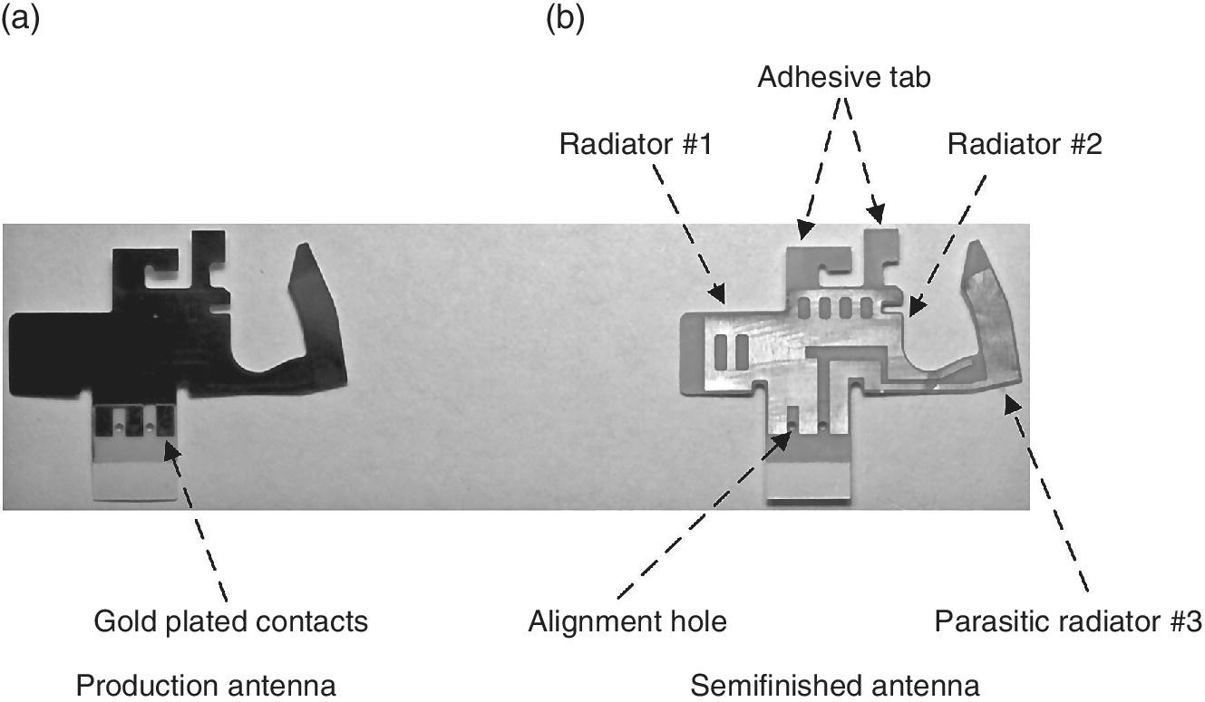
Figure 4.101 Hongmi 2A’s secondary antenna.
(Source: Reproduced with permission of Xiaomi, Inc. and Shanghai Amphenol Airwave, Inc.)
Shown in Figure 4.102 is a semifinished secondary antenna, which has been installed on the top‐left corner of a plastic frame. Some portion of the flex, which has three gold plated contacts, is passed through the slit on the plastic frame and wrapped to its back.

Figure 4.102 Semifinished secondary antenna installed on a phone.
(Source: Reproduced with permission of Xiaomi, Inc. and Shanghai Amphenol Airwave, Inc.)
Shown in Figure 4.103 is a zoom‐in photo of the matching circuit of the secondary antenna. There are three spring fingers on the PCB. Spring finger 1 connects to the parasitic element. Spring fingers 2 and 3 connect to the IFA. Both spring fingers 1 and 3 are shorted to ground through 0 Ω resistors. Those two 0 Ω resistors are not necessary in the design and spring fingers can be grounded directly. However, those resistors can be replaced by inductors or capacitors to fine‐tune antenna, which might be helpful. Using the parasitic element as an example, by replacing the 0 Ω resistor connected to spring finger 1 with an inductor, the element’s resonant frequency can be tuned lower. An inductor with larger value shifts frequency more. On the other hand, a capacitor can shift frequency higher. A capacitor with smaller value shifts frequency more.

Figure 4.103 Matching circuit of the secondary antenna.
(Source: Reproduced with permission of Xiaomi, Inc.)
Unless it is an emergency, try to avoid using this tuning method. Either inductors or capacitors have inherent loss, which decreases the overall antenna efficiency. It is a better practice to tune antenna through adjusting radiator length.
Spring finger 2 connects to a π‐shaped matching network. There are three pairs of solder pads (one shunt, one series, and one shunt) on the PCB. It seems that the antenna is tuned pretty well and no matching is used in the final design. A 0 Ω resistor is placed on the series pad to simply make galvanic connection.
Shown in Figure 4.104 are photos of the WLAN and GPS antenna. Figure 4.104a is a production antenna. Figure 4.104b is a semifinished antenna, which is provided for a better view of different radiators. This antenna covers two frequency bands: 1.575 GHz (GPS) and 2.4−2.482 GHz (802.11b/g/n and Bluetooth). It adopts a dual‐band IFA design. Radiator 2 is the longer trace and responsible for the GPS band. Radiator 1 takes care of the higher band.

Figure 4.104 Hongmi 2A’s WLAN and GPS antenna.
(Source: Reproduced with permission of Xiaomi, Inc. and Shanghai Amphenol Airwave, Inc.)
Shown in Figure 4.105 is a semifinished WLAN and GPS antenna, which has been installed on the top‐right corner of a plastic frame. Some portion of the flex, which has two gold plated contacts, is passed through the slit on the plastic frame and wrapped to its back.

Figure 4.105 Semifinished WLAN and GPS antenna installed on a phone.
(Source: Reproduced with permission of Xiaomi, Inc. and Shanghai Amphenol Airwave, Inc.)
Shown in Figure 4.106 is a zoom‐in photo of the matching circuit of the WLAN and GPS antenna. There are two spring fingers on the PCB. The spring finger 1 connects to ground directly. The spring finger 2 connects to a π‐shaped matching network, which is similar to the one used in the secondary antenna. It seems that the WLAN and GPS antenna is also pretty well tuned. No matching component is used and only a 0 Ω resistor is placed on the series pad to make galvanic connection.

Figure 4.106 Matching circuit of the WLAN and GPS antenna.
(Source: Reproduced with permission of Xiaomi, Inc.)
Shown in Figure 4.107 are switch connectors of the primary and the secondary antennas. Detailed discussion about switch connector can be found in Section 5.1.2.1. Because the impedance of a switch connector is always 50 Ω, it is an ideal place to tap in a coaxial cable for passive antenna measurement. No matter whether it is a 2G, 3G, or 4G phone; all phones have switch connectors on the signal paths of cellular antennas. The switch connector is used to measure a phone’s RF circuit; it can’t be used to measure antenna directly.

Figure 4.107 Switch connectors on the PCB.
(Source: Reproduced with permission of Xiaomi, Inc.)
4.10.2 Flagship Phone
Shown in Figure 4.108 are front, side, and back views of Xiaomi 4. The starting price of this phone is 1999 RMB, which is around 317 USD, when purchased without a contract. Xiaomi 4 was released in June, 2014. It has a 5 inch 1920 × 1080 IPS screen, 3GB ram, and 16GB flash memory.

Figure 4.108 Xiaomi 4.
(Source: Reproduced with permission of Xiaomi, Inc.)
To convince a customer to buy a high‐end phone, which costs several times more than an entry‐level phone, faster CPU and GPU, larger memory, higher resolution LCD, and better camera are all essential. However, the most important aspect above all is its appearance, because most customers can’t even tell what GPU stands for.
A high‐end phone must look like a luxury item. One iconic feature of an high‐end phone is its metallic frame. For antenna engineers, metal frames make designing job much more challenging. Apple has patented hybrid slot antenna solutions [44–46]by using the gap between a whole metal frame and PCB inside a phone. This technique has been used in iPhone 3G and 3Gs. Since the advent of iPhone 4, Apple adopted a new approach which is cutting slits on the metal frame. By cutting several slits on the phone frame, from antenna point of view, the frame is actually several isolated metal pieces, which gives antenna designing much more freedom. Recently, big screen phones become the new normal, which actually makes available area for antenna designing much larger. People start to revisit the idea of using the gap between a whole metal frame and inner PCB to designing antennas [47, 48].
Xiaomi 4 adopts the approach of cutting slits on the metal frame. It is obvious there are four slits: two on the top edge and two on the bottom edge.
Shown in Figure 4.109 is the front and back photos of Xiaomi 4’s antennas. Because the battery of Xiaomi 4 is unexchangeable, its back cover is also not supposed to be removed. Unlike Hongmi 2A, all three antennas are not masked by black paint. Xiaomi 4’s antennas are manufactured by using LDS technologies, which has been discussed in Section 4.2.5. The Xiaomi 4 supports both 2.4 and 5 GHz WLAN band. The cellular bands which are supported by Xiaomi 4 are listed in the following:
| 4G TDD‐LTE | B38 (2570–2620 MHz) |
| B39 (1880–1920 MHz) | |
| B40 (2300–2400 MHz) | |
| 3G TD‐SCDMA | B34 (2010–2025 MHz) |
| B39 (1880–1920 MHz) | |
| 2G GSM bands | B2 (1850–1990 MHz) |
| B3 (1710–1880 MHz) | |
| B8 (880–960 MHz) |

Figure 4.109 Xiaomi 4’s antennas.
(Source: Reproduced with permission of Xiaomi, Inc.)
Shown in Figure 4.110 is a PCB of Xiaomi 4. Similar to Hongmi 2A, there are three sets of spring fingers for the primary, secondary, and WLAN antennas, respectively. There are also three switch connectors. Different from Hongmi 2A, Xiaomi 4’s WLAN antenna has its own switch connector. More discussion can be found in Section 6.1.4, the short version explanation is that the new SAR regulation now requires measurements on WLAN bands. To carry out a SAR evaluation, the conducted power, which is measured through a switch connector, must be recorded first. Xiaomi 4 also adopts the design of bottom primary antenna. A coaxial cable is used to connect the antenna to the main PCB on the top. Both the primary and secondary antennas have grounding springs, which are part of antenna structure and different from Hongmi 2A.

Figure 4.110 Xiaomi 4’s PCB.
(Source: Reproduced with permission of Xiaomi, Inc.)
Shown in Figure 4.111 is the primary antenna. This antenna is a variation of loop antenna, which has been discussed in Section 4.4. Actually, the antenna on the plastic cover can’t function by itself. It might be difficult to observe, but there is a closed loop embedded in the structure. The loop path, marked as A‐A′‐B′‐B‐Metal Frame‐C‐D‐E in Figure 4.111, passes through the antenna, metal frame, and PCB.

Figure 4.111 Xiaomi 4’s primary antenna.
(Source: Reproduced with permission of Xiaomi, Inc.)
Following a detailed description of the loop path. The bottom portion of Xiaomi 4’s metal frame is broken into three pieces by two slits. One slit is next to point B and the other is next to point C. Because of these two slits, the middle portion is isolated from the rest of the metal frame. Points B and C are exposed inner surfaces of the floating metal frame. Point B′ on the antenna connects to point B on the metal frame. Because the LDS antenna can’t provide required spring force, a separate spring fingers is installed at point B′.
Point D on the PCB connects to point C on the metal frame through a grounding spring. The grounding spring was designed to provide required spring force on both points C and D. Both points D and E are on the system ground and automatically connected.
Point A is the center spring fingers on the PCB. It is also the feeding point of the antenna. Point A connects the back of the antenna. There are two metalized strips on the back of the antenna, as shown in Figure 4.109. The right strip connects to point A′ through a metalized hole, which is similar to a via on PCB.
Besides the loop antenna, there is a parasitic antenna. The parasitic antenna connects to the right spring finger on the PCB through another metalized hole. The right spring finger is connected to system ground through a 0 Ω resistor. It can be seen that there are three though holes on the structure. The left one is not metalized and there is also no metal strip on the back. As has been discussed in Hongmi 2A, this is a redundant feature and is left there just in case.
The antenna has a five‐element matching network, but only has three components been populated. Starting from the center spring finger, there is a shunt inductor, a series inductor, and a 0 Ω series resistor. The coaxial cable that connects to the matching network is the cable shown in Figure 4.109. The left spring finger is also connected to system ground through a 0 Ω resistor; however, it is a floating finger and does not connect to anything.
Shown in Figure 4.112 is the secondary antenna. This antenna is also a variation of loop antenna. Similar to the main antenna, there is a loop path, which is marked as A‐A′‐B′‐B‐Metal Frame‐C‐D‐E in Figure 4.112, passes through the antenna, metal frame, and PCB. This loop is almost identical to the main antenna. Two slits on both sides separate the metal frame to three pieces. The middle portion of the metal frame becomes part of the loop.

Figure 4.112 Xiaomi 4’s secondary antenna.
(Source: Reproduced with permission of Xiaomi, Inc.)
Similar to the main antenna, there are also three spring fingers beneath the secondary antenna. This time, the right finger is the redundant one. The left finger is connected to system ground through a 0 Ω resistor. This generates two extra loops, marked as loop 1 and loop 2 in Figure 4.112, between feeding point and system ground. Loop 1 is relatively small, so it likely provides matching in the lower band, which is similar to what IFA’s grounding branch does. Loop 2 is reasonably large and might function as an extra loop antenna at the higher frequency band.
There is one interesting feature, which is marked as the 4th spring finger in Figure 4.112. This 4th finger is also connected to system ground. The finger connects to the metal frame of the back camera. If we look at Figure 4.109, there is significant overlap between antenna and camera’s metal frame. It seems that the metal frame has been used as a parasitic antenna.
Shown in Figure 4.113 is the WLAN, etc. antenna. Xiaomi 4 supports GPS, Bluetooth, 2.4, and 5 GHz WLAN. The third antenna needs to cover all three bands. This antenna is a variant of IFA design. There are two spring fingers on the PCB. The top spring finger is the feeding point and the bottom one is the grounding point. Radiator 1 can generate the lowest band, GPS band. Radiator 2 and higher order mode from radiator 1 can take care of 2.4 and 5 GHz bands. There are only two through hole on the antenna. Both of them are metalized. Although there is a preserved matching network on the PCB, no matching component is populated. Only two series 0 Ω resistors are used to make the connection.

Figure 4.113 Xiaomi 4’s WLAN, etc. antenna.
(Source: Reproduced with permission of Xiaomi, Inc.)
Contents in Section 4.10 are the author’s observations. Xiaomi Inc. has kindly provided phones, and Shanghai Amphenol Airwave Inc. has kindly provided antenna parts. To avoid conflict of interest or unnecessary leaking of trade secrets, all materials are provided as it is. None of the observation has been confirmed by these two companies. On the other hand, the author has not verified any observation by experiment or simulation. It is recommended that readers only use this section as a general reference.
References
- [1] Wong, K.‐L. (2003) Planar Antennas for Wireless Communications, Wiley‐Interscience.
- [2] Arkko, A.T. (2003) Effect of ground plane size on the free‐space performance of a mobile handset PIFA antenna. 12th International Conference on Antennas and Propagation, 2003. (ICAP 2003). (Conf. Publ. No. 491), vol. 1, pp. 316–319.
- [3] Chan, K.H., Fung, L.C., Leung, S.W., and Siu, Y.M. (2006) Effect of internal patch antenna ground plane on SAR. 17th International Zurich Symposium on Electromagnetic Compatibility, 2006. EMC‐Zurich 2006, pp. 513–516.
- [4] Fujio, S. (2006) Effect of ground size on plate inverted‐F antenna. IEEE International Workshop on Antenna Technology Small Antennas and Novel Metamaterials, 2006, pp. 269–272.
- [5] Urban, R. and Peixeiro, C. (2004) Ground plane size effects on a microstrip patch antenna for small handsets. 15th International Conference on Microwaves, Radar and Wireless Communications, 2004. MIKON‐2004., vol. 2, pp. 521–524.
- [6] Wong, K.‐L. (2002) Compact and Broadband Microstrip Antennas, Wiley‐Interscience.
- [7] Balanis, C.A. (2005) Antenna Theory: Analysis and Design, 3rd edn, Wiley‐Interscience.
- [8] Iskander, M.F. (2000) Electromagnetic Fields and Waves, 1st edn, Waveland Press Inc.
- [9] Sadiku, M.O. (2009) Elements of Electromagnetics, 5th edn, Oxford University Press, USA.
- [10] Ulaby, F.T., Michielssen, E., and Ravaioli, U. (2010) Fundamentals of Applied Electromagnetics, 6th edn, Prentice Hall.
- [11] Buck, J. and Hayt, W. (2005) Engineering Electromagnetics, 7th edn, McGraw‐Hill Science/Engineering/Math.
- [12] Chi, Y.W. and Wong, K.‐L. (2007) “Internal compact dual‐band printed loop antenna for mobile phone application,” IEEE Transactions on Antennas and Propagation, 55, 1457–1462.
- [13] Wong, K.‐L. and Huang, C.‐H. (2008) “Printed loop antenna with a perpendicular feed for pentaband mobile phone application,” IEEE Transactions on Antennas and Propagation, 56, 2138–2141.
- [14] Chi, Y.‐W. and Wong, K.‐L. (2008) “Compact multiband folded loop chip antenna for small‐size mobile phone,” IEEE Transactions on Antennas and Propagation, 56, 3797–3803.
- [15] Chi, Y.‐W. and Wong, K.‐L. (2009) “Quarter‐wavelength printed loop antenna with an internal printed matching circuit for GSM/DCS/PCS/UMTS operation in the mobile phone,” IEEE Transactions on Antennas and Propagation, 57, 2541–2547.
- [16] Almpanis, G., Fumeaux, C., and Vahldieck, R. (2006) “Offset cross‐slot‐coupled dielectric resonator antenna for circular polarization,” IEEE Microwave and Wireless Components Letters, 16, 461–463.
- [17] Guha, D. and Antar, Y.M.M. (2006) “New half‐hemispherical dielectric resonator antenna for broadband monopole‐type radiation,” IEEE Transactions on Antennas and Propagation, 54, 3621–3628.
- [18] Leung, K.W., Tse, K.K., Luk, K.M., and Yung, E.K.N. (1999) “Cross‐polarization characteristics of a probe‐fed hemispherical dielectric resonator antenna,” IEEE Transactions on Antennas and Propagation, 47, 1228–1230.
- [19] Chang, T.‐H. and Kiang, J.‐F. (2007) “Dualband split dielectric resonator antenna,” IEEE Transactions on Antennas and Propagation, 55, 3155–3162.
- [20] Chang, T.‐H. and Kiang, J.‐F. (2009) “Bandwidth broadening of dielectric resonator antenna by merging adjacent bands,” IEEE Transactions on Antennas and Propagation, 57, 3316–3320.
- [21] Wong, K.L., Chen, N.C., and Chen, H.T. (1993) “Analysis of a hemispherical dielectric resonator antenna with an airgap,” IEEE Microwave and Guided Wave Letters, 3, 355–357.
- [22] Chen, Y.C., Lin, J.Y., and Tsao, S.M. (2007) Planar patch antenna using temperature stable high‐permittivity ceramics. IEEE Conference on Electron Devices and Solid‐State Circuits, 2007. EDSSC 2007, pp. 761–764.
- [23] Hauser, R., Fachberger, R., Bruckner, G. et al. (2005) Ceramic patch antenna for high temperature applications. 28th International Spring Seminar on Electronics Technology: Meeting the Challenges of Electronics Technology Progress, 2005, pp. 173–178.
- [24] Natashah, N.M., Muammar, M.I., Soh, P.J. et al. (2008) Design of a microstrip patch antenna using low temperature co‐fired ceramic technology. International Conference on Electronic Design, 2008, pp. 1–3.
- [25] Kula, J.S., Psychoudakis, D., Liao, W.J. et al. (2006) “Patch‐antenna miniaturization using recently available ceramic substrates,” IEEE Antennas and Propagation Magazine, 48, 13–20.
- [26] Booker, H.G. (1946) “Slot aerials and their relation to complementary wire aerials,” Journal of the Institution of Electrical Engineers, Part III A, 620–626.
- [27] Deng, C., Li, Y., Zhang, Z., and Feng, Z. (2015) “A novel low‐profile Hepta‐band handset antenna using modes controlling method,” IEEE Transactions on Antennas and Propagation, 63, 799–804.
- [28] Lee, S., Jung, H., and Sung, Y. (2015) “A reconfigurable antenna for LTE/WWAN mobile handset applications,” IEEE Antennas and Wireless Propagation Letters, 14, 48–51.
- [29] Mun, B., Jung, C., Park, M., and Lee, B. (2014) “A compact frequency‐reconfigurable multiband LTE MIMO antenna for laptop applications,” IEEE Antennas and Wireless Propagation Letters, 13, 1389–1392.
- [30] Sung, Y., (2012) “Compact quad‐band reconfigurable antenna for mobile phone applications,” Electronics Letters, 48, 977–979.
- [31] Li, Y., Zhang, Z., Zheng, J. et al. (2012) “A compact Hepta‐band loop‐inverted F reconfigurable antenna for mobile phone. IEEE Transactions on Antennas and Propagation, 60, 389–392.
- [32] “MIMO (Multiple Input Multiple Output),” http://www.sharetechnote.com/html/BasicProcedure_LTE_MIMO.html. Retrieved 25 October 2015.
- [33] Goldsmith, A., Jafar, S., Jindal, N., and Vishwanath, S. (2003) “Capacity limits of MIMO channels,” IEEE Journal on Selected Areas in Communications, 21, 684–702.
- [34] Applebaum, S. (1976) “Adaptive array,” IEEE Transactions on Antennas and Propagation, 24, 585–598.
- [35] Vaughan, R.G. and Andersen, J. (1987) “Antenna diversity in mobile communications,” IEEE Transactions on Vehicular Technology, 36, 149–172.
- [36] Fujimoto, K. and James, R. (2001) Mobile Antenna Systems Handbook, 2rd edn, Artech House.
- [37] Blansh, S., Romeu, J., and Corbella, I. (2003) “Exact representation of antenna system diversity performance form input parameter description,” Electronics Letters, 39, 705–707.
- [38] Zhong, H., Zhang, Z., Chen, W. et al. (2009) “A tri‐polarization antenna fed by proximity coupling and probe,” IEEE Antennas and Wireless Propagation Letters, 8, 465–467.
- [39] Li, Y., Zhang, Z., Chen, W. et al. (2010) “A dual‐polarization slot antenna using a compact CPW feeding structure,” IEEE Antennas and Wireless Propagation Letters, 9, 191–194.
- [40] Li, Y., Zhang, Z., and Feng, Z. (2011) “Dual‐polarised monopole‐slot co‐located MIMO antenna for small‐volume terminals,” Electronics Letters, 47, 1259–1260.
- [41] Li, Y., Zhang, Z., Zheng, J., and Feng, Z. (2012) “Compact azimuthal omnidirectional dual‐polarized antenna using highly isolated colocated slots,” IEEE Transactions on Antennas and Propagation, 60, 4037–4045.
- [42] Wang, Y. and Du, Z. (2013) “A wideband printed dual‐antenna system with a novel neutralization line for mobile terminals,” IEEE Antennas and Wireless Propagation Letters, 12, 1428–1431.
- [43] “3GPP Specification Detail 36.306,” http://www.3gpp.org/DynaReport/36306.htm. Retrieved 25 October 2015.
- [44] Zhang, Z., Schlub, R., Hill, R., and Caballeo, R. (2009) Multiband antenna for handheld electronic devices. US7768462B2.
- [45] Zhang, Z., Hill, R., and Schlub, R. et al. (2010) Hybrid antennas with directly fed antenna slots for handheld electronic devices. US7551142B1.
- [46] Zhang, Z., Chen, W., Feng, Z., and Iskander, M. (2008) “Integrated dual‐band antenna system design incorporating cell phone bezel,” IEEE Antennas and Wireless Propagation Letters, 7, 585–587.
- [47] Ban, Y., Qiang, Y., Chen, Z. et al. (2015) “A dual‐loop antenna design for Hepta‐band WWAN/LTE metal‐rimmed smartphone applications,” IEEE Transactions on Antennas and Propagation, 63, 48–58.
- [48] Hsu, C. and Chung, S. (2015) “Compact multiband antenna for handsets with a conducting edge,” IEEE Transactions on Antennas and Propagation, 63, 5102–5107.