
Basic Amplifier Tests
This chapter is devoted to basic tests for amplifier circuits. These procedures can be applied to a complete amplifier circuit (such as a stereo system) or to specific circuits (such as the IC-amplifier circuit designs described in the remaining chapters). The procedures also can be applied to amplifier circuits at any time during design or experimentation. As a minimum, the tests should be made when the circuit is first completed in experimental form. If the test results are not as desired, the component values can be changed as necessary to obtain the desired results. The circuit can then be retested in final form (with all components and ICs soldered in place). This shows if there is any change in circuit performance because of physical relation of components (a common problem). Additional test procedures for specific types of IC amplifiers are given in the related chapters. Keep in mind that all amplifiers need not be subjected to all tests described in this book. However, if an amplifier circuit produces the desired results for all the tests, the circuit can be considered a successful design.
2.1 Amplifier Test Equipment
The tests described in this chapter can be performed using meters, scopes, generators, power supplies, and assorted clips, patch cords, etc. Therefore, if you have a good set of test equipment that is suitable for other electronic work, you can probably get by. A possible exception is a distortion meter (especially if you are interested in audio amplifiers). Some points you should consider when selecting and using test equipment are discussed below.
2.1.1 Matching Test Equipment to the Circuits
No matter what test instrument is involved, try to match the capabilities of the test equipment to the circuit. For example, if pulses, square waves, or complex waves are to be measured (as they are in any IC amplifier test), a peak-to-peak meter can possibly provide meaningful indications, but a scope is the logical instrument. (This chapter concludes with a series of notes on matching test equipment to IC amplifiers.)
2.1.2 Voltmeters/Multimeters
In addition to making routine voltage and resistance checks, the main functions for a meter in amplifier work are to measure frequency response and to trace signals from input to output. Many technicians prefer scopes for these procedures. The reasoning is that scopes also show distortion of the waveforms during measurement or signal tracing. Other technicians prefer the simplicity of a meter, particularly in such procedures as voltage-gain and power-gain measurements.
It is possible that you can get by with any AC meter (even a basic multimeter, analog or digital) for all amplifier work. However, for accurate measurements, use a wideband meter, preferably a dual-channel model. (Obviously, the meter must have a bandwidth greater than the amplifier circuit being tested!) The dual-channel feature makes it possible to monitor both channels of a stereo circuit simultaneously. This is particularly important for stereo frequency-response and crosstalk measurements, but is of no great importance for nonstereo amplifiers.
2.1.3 Scopes
If you have a good scope for TV and VCR work, use that scope for all amplifier-circuit measurements. If you are considering a new scope, remember that a dual-channel instrument permits you to monitor both channels of a stereo circuit (as is the case with a dual-channel voltmeter). It is of greater importance that a dual-channel scope lets you monitor the input and output of an amplifier simultaneously. Many examples of this technique are given throughout this book. A scope also has the advantages over a meter in that it can display such common IC amplifier conditions as distortion, hum, ripple, overshoot, and oscillation, and is an indispensable tool for measuring such characteristics as settling time, slew rate, and noise. (However, the meter is easier to read when you are concerned only with gain.)
2.1.4 Distortion Meters
If you are already in audio/stereo work, you probably have distortion meters (and know how to use them effectively). There are two types of distortion measurements: harmonic and intermodulation. No particular meter is described here. Instead, descriptions are included of how harmonic and intermodulation distortion measurements are made.
2.2 Decibel Measurement Basics
The decibel is widely used in amplifier work to express logarithmically the ratio between two power or voltage levels. For example, a typical IC op-amp data sheet lists voltage gain, power gain, and common-mode rejection ratio in decibels. The decibel is one tenth of a bel. (The bel is too large for most practical applications.)
Although there are many ways to express a ratio, the decibel is used in amplifiers for two reasons: it is a convenient unit to use for all types of amplifiers and it is related to the reaction of the human ear and is thus well suited for use with audio amplifiers.
Humans can listen to ordinary conversation quite comfortably and yet be able to hear thunder (which is taken to be 100,000 times louder than conversation) without damage to the ear. This is because the response of the human ear to sound waves is approximately proportional to the logarithm of the sound-wave energy and is not proportional to the energy.
The common logarithm (log10) of a number is the number of times 10 must be multiplied by itself to equal that number. For example, the logarithm of 100 (that is, 10 × 10, or 102) is 2. Likewise, the logarithm of 100,000 (105) is 5. This relationship is written log10 100,000 = 5.
In comparing two powers, it is possible to use the bel (which is the logarithm of the ratio of the two powers). For example, in comparing the power of ordinary conversation with that of thunder, the increase in sound is equal to
Using the more convenient decibel, the increase in sound from ordinary conversation to thunder is equal to
For convenience, the same method is used in measuring the increase in amplifier power, whether the amplifiers are used with audio frequencies or not. The increase in power of any amplifier can be expressed as
This relationship can also be expressed as
Usually, P2 represents power output and P1 represents power input. If P2 is greater than P1, there is a power gain, expressed in positive decibels (+dB). With P1 greater than P2, there is a power loss, expressed in negative decibels (−dB). Whichever is the case, the ratio of the two powers (P1 and P2) is taken, and the logarithm of this ratio is multiplied by 10. As a result, power ratio of 10 = 10-dB gain, power ratio of 100 = 20-dB gain, power ratio of 1,000 = 30-dB gain, etc.
2.2.1 Doubling Power Ratios
Doubling the power of an amplifier produces a power gain of +3 dB. For example, if the volume control of an amplifier is turned up so that the power rises from 4 to 8 W, the gain is up +3 dB. If the power output is reduced from 4 to 2 W, the gain is down −3 dB.
If the original 4 W is increased to 8 W, the power gain is +3 dB. Increasing the power output further to 16 dB produces another gain of +3 dB, with a total power gain of +6 dB. At 40 W, the power is increased 10 times (from the original 4 W), the total power gain is +10 dB, and so on.
2.2.2 Adding Decibels
There is another convenience in using decibels for amplifier work. When several amplifier stages are connected so that one works into another (stages connected in cascade, as is the usual case in IC amplifiers), the gains of each stage are multiplied. For example, if three stages, each with a gain of 10, are connected, there is a total power gain of 10 × 10 × 10, or 1,000.
In the decibel system, the decibel gains are added. Using our example, the decibel power gain is 10 + 10 + 10, or +30 dB. Similarly, if two amplifier stages are connected, one of which has a gain of +30 dB and the other a loss of −10 dB, the net result is +30 −10, or +20 dB.
2.2.3 Using Decibels to Compare Voltages and Currents
The decibel system is also used to compare the voltage input and output of an amplifier. (Decibels can be used to express current ratios. However, this is generally not practical in amplifiers.) When voltages (or currents) are involved, the decibel is a function of
The ratio of the two voltages (or currents) is taken, and the logarithm of this ratio is multiplied by 20.
It is important to note that although power ratios are independent of source and load impedance values, voltage and current ratios in these equations hold true only when the source and load impedances are equal.
In amplifiers where input and output impedances differ, voltage and current ratios are calculated as follows:
where R1 is the source or input impedance and R2 is the load or output impedance. (E1 ![]() and I1
and I1 ![]() are always higher in value than E2
are always higher in value than E2 ![]() and I2
and I2 ![]() .)
.)
As is true for the power relationship, if the voltage output is greater than the input, there is a decibel gain (+dB). If the output is less than the input, there is a voltage loss (–dB).
Note that doubling the voltage produces a gain of +6 dB. Conversely, if the voltage is cut in half, there is a loss of −6 dB. To get the net effect of several voltage-amplifier stages working together, add the decibel gains (or losses) of each.
2.2.4 Decibels and Reference Levels
When an amplifier has a power gain of + 20 dB, this has no meaning in actual power output. Instead, it means that the power output is 100 times as great as the power input. For this reason, decibels are often used with specific reference levels.
The most common reference levels for audio amplifiers are the volume unit, or VU, and the decibel meter, or dBm.
When VU is used, it is assumed that the zero level is equal to 0.001 (1 mW) across a 600-ohm impedance. Thus,
Both the dBm and VU have the same zero level base. A dBm scale is (generally) found on meters when the signal to be measured is a sine wave (normally 1 kHz), whereas the VU is used for complex audio waveforms.
2.3 Frequency Response
Amplifier frequency response can be measured with a generator and a meter or scope. The generator is tuned to various frequencies, and the resultant output response is measured at each frequency. The results are then plotted in the form of a graph or response curve. Figure 2-1 shows the test connections to measure open-loop gain (AOL) for a typical op-amp (a Harris CA3100). The term open-loop gain applies to the IC-amplifier gain without feedback. Figures 2-2 and 2-3 show the frequency response for various power-supply voltages and temperatures, respectively.

FIGURE 2-1 Open-loop voltage gain test circuit and offset-adjust circuit (Harris Semiconductors, Linear & Telecom ICs, 1994, p. 2–106)

FIGURE 2-2 Open-loop gain versus frequency (Harris Semiconductors, Linear & Telecom ICs, 1994, p. 2–104)

FIGURE 2-3 Open-loop gain versus frequency at different temperatures (Harris Semiconductors, Linear & Telecom ICs, 1994, p. 2–104)
As shown, gain (at any given frequency) varies directly with supply voltage and inversely with temperature for this amplifier. These variations must be considered in design. For example, if this particular amplifier is to be used at 1 MHz and the maximum available supply voltage is 7 V, the maximum open-loop gain is about 30 dB. If an 18-V supply is available, a gain of 45 dB is possible, all other factors being the same.
The frequency at which the output begins to drop is called the rolloff point. In the amplifier of Figs. 2-2 and 2-3, rolloff starts at a frequency just below 0.1 MHz. The specifications for some IC amplifiers consider the rolloff point to start when the output drops 3 dB below the flat portion of the curve.
The curves of Figs. 2-2 and 2-3 show the open-loop rolloff and gain-frequency relationship of the IC, without any external compensation. As discussed in Chapter 3, some IC amplifiers provide for connection of an external compensation circuit (usually a capacitor, but sometimes a capacitor-resistor combination). Such compensation circuits alter both the rolloff point and the gain-frequency relationship. Figure 2-4 shows how the output characteristics are altered when an external compensating capacitor is added to the circuit of Fig. 2-1. Also, as discussed in Chapter 3, many IC amplifiers have built-in compensation, so the open-loop characteristics cannot be altered.

FIGURE 2-4 Open-loop gain and phase shift versus frequency (Harris Semiconductors, Linear & Telecom ICs, 1994, p. 2–104)
The basic procedure for measuring frequency response is to apply a constant-amplitude signal while monitoring the output. The input signal is varied in frequency (but not in amplitude) across the entire operating range of the amplifier. The voltage output at various frequencies across the range is then plotted on the graph as follows.
1. Connect the equipment as shown in Fig. 2-1. Keep in mind that Fig. 2-1 shows the connection for a specific IC amplifier. However, the circuit has all of the basic elements of a typical open-loop gain test circuit. The inverting input is grounded, and the test signal is applied to the noninverting input. Thus, the output should be an amplified, noninverting version of the input. The input is terminated in an impedance equal to that of the signal source (51 ohms). The output is terminated at some specific test values (2 k and 20 pF).
Note that the 20-pF capacitor is not used for the graph of Fig. 2-3, but is used for both Figs. 2-2 and 2-4. The compensating capacitor is used only for the graph of Fig. 2-4. The output load resistance is used for all three graphs. From a design standpoint, it is important to remember that the IC amplifier characteristics will change (sometimes drastically) with changes in output load. Therefore, if the data sheet test values are not close to those of the real load, try testing the IC with real-world values at the output, in addition to the test with the data sheet values. (You may find that the IC will not meet your particular gain-frequency or rolloff requirements!)
2. Initially, set the generator frequency to the low end of the range (about 1 kHz for our IC amplifier), then set the generator amplitude to the desired input level. In the absence of a realistic test input voltage, set the generator output to an arbitrary value.
A simple method of finding a satisfactory input level is to monitor the circuit output and increase the generator amplitude at the amplifier center frequency (at 1 MHz for our IC) until the amplifier is overdriven. This point is indicated when further increases in generator output do not cause further increases in meter reading (or the output waveform peaks begin to flatten on the scope display). Set the generator output just below this point. Then, return the meter or scope to monitor the generator voltage (at the circuit input) and measure the voltage. Keep the generator at this voltage throughout the test.
3. If the circuit is provided with any operating or adjustment controls (volume, loudness, gain, treble, bass, balance, and so on), set the controls to some arbitrary point when making the initial frequency-response measurement. The response measurements can then be repeated at different control settings, if desired. Although there are no controls, as such, in our test circuit, Fig. 2-1 does provide for a null adjustment. As discussed in Section 1.15, if there is an unbalance in the differential input of the IC, or if there is a level shift in the stages following the input, the output might not be zero with a zero input. This can be corrected by adjustment of RX as shown in Fig. 2-1. Short pin 3 to pin 2 (or ground), and adjust RX for a zero output, with no signal applied.
4. Record the amplifier output voltage on the graph. Without changing the generator amplitude, increase the generator frequency by some fixed amount and record the new amplifier output voltage. The amount of frequency increase is an arbitrary matter. For example, in an audio amplifier, use an increase of 10 Hz at frequencies where rolloff occurs and 1 kHz at the middle frequencies. These values can be increased by 10 for our IC.
5. After the initial frequency-response check, check the effect of operating or adjustment controls (if any). For example, in an audio amplifier, the volume, loudness, and gain controls should have the same effect across the entire frequency range. Treble and bass controls might have some effect on all frequencies. However, a treble control should have the greatest effect at the high end, whereas bass controls should be most effective at the low end.
6. Remember that generator output can vary with changes in frequency (a fact this is possibly overlooked in making frequency-response tests). Monitor the generator output amplitude after each change in frequency. It is essential that the generator output amplitude remain constant over the entire frequency range of the test.
2.4 Voltage Gain
Voltage gain for an amplifier is measured in the same way as frequency response. The ratio of output voltage VO to input voltage VI (at any given frequency or across the entire frequency range) is the voltage gain. In this case, we are measuring open-loop gain, or AOL. Because the input voltage (generator output) is held constant for a frequency-response test, a voltage-gain curve should be identical to a frequency-response curve (such as shown in Figs. 2-2, 2-3, and 2-4).
2.5 Power Output and Power Gain
Power output of an amplifier is found by noting the output voltage across the load resistance at any frequency across the entire frequency range. For example, in the circuit of Fig. 2-1, if the output voltage VO is 10 V, the power is P = E2/R = 102/2,000 = 100/2,000 = 0.05 W or 50 mW. As a practical matter, never use a wire-wound component (or any component that has reactance) for the load resistance. Reactance changes with frequency and causes a load to change. Use a composition resistor or potentiometer for the load.
To find the power gain of an amplifier, start by finding both the input and output power. Input power is found in the same way as output power, except that the input impedance must be known (or calculated). Calculating input impedance is not practical in some circuits, especially in designs where input impedance depends on transistor gain (the procedure for finding dynamic input impedance is described in Section 2.9). With input power known (or estimated), power gain is the ratio of output power to input power.
2.6 Input Sensitivity
In some amplifier circuits, an input sensitivity specification is used in place of or in addition to power-output/gain specifications. Input sensitivity implies a minimum power output with a given voltage input (such as 10-W output with a 100-mV input). Input sensitivity usually applies to power amplifier. To find input sensitivity, simply apply the specified input and note the actual power output.
2.7 Bandwidth
Some amplifier specifications require that the circuit deliver a given voltage or power output across a given frequency range. Usually, the voltage bandwidth is not the same as the power bandwidth. For example, an amplifier might produce full-power output up to 20 kHz, even though the frequency response is flat up to 100 kHz. That is, voltage (with a load) remains constant up to 100 kHz, whereas power output (across a normal load) remains constant up to 20 kHz. Figure 2-5 shows the test connections and procedures to measure bandwidth at − 3 dB points for a typical op-amp (a Harris CA3020/CA3020A).

2.8 Load Sensitivity
Most amplifiers are sensitive to changes in load. This is particularly true of power amplifiers. An amplifier produces maximum power when the output impedance is the same as the load impedance. The test circuit for load-resistance measurement is the same as for frequency response (Fig. 2-1), except that the load resistance is variable. Again, never use a wire-wound load resistance. The reactance can result in considerable error.
To find load sensitivity, measure the power output at various load-impedance and output-impedance ratios. That is, set the load resistance to various values (including a value equal to the supposed amplifier-output impedance). Record the voltage and/or power gain at each setting. Repeat the test at various frequencies. Figure 2-6 shows a typical load-sensitivity response curve. Notice that if the load is twice the output impedance (as indicated by a 2:1 ratio, or a normalized load impedance of 2), the output power is reduced to about 50%.

2.9 Dynamic Output Impedance or Resistance
The load-sensitivity test can be reversed to find the dynamic output impedance or resistance of an amplifier. The connections (Fig. 2-1) and procedures are the same, except that the load resistance is varied until maximum power output is found. Power is removed, the load resistance is disconnected from the circuit, and the resistance is measured with an ohmmeter. This resistance is equal to the dynamic output impedance of the circuit (but only at that measurement frequency). This test can be repeated across the entire frequency range, if required.
2.10 Dynamic Input Impedance or Resistance
Use the circuit and procedures shown in Fig. 2-7 to find the dynamic input impedance or resistance of an amplifier. Note that the IC shown in Fig. 2-7 has two inputs to be measured. Also note that the accuracy of this impedance measurement (and the output impedance measurement) depends on the accuracy with which the resistance R is measured. Again, a noninductive (not wire-wound) resistance must be used for R. The impedance found by this method applies only to the frequency used during the test.

2.11 Current Drain, Power Output, Efficiency, and Sensitivity
Figure 2-8 shows a circuit and the procedures suitable for measuring zero-signal DC current drain, maximum-signal DC current drain, maximum power output, circuit efficiency, sensitivity, and transducer power gain. Again, the circuit of Fig. 2-8 applies to a specific IC amplifier (Harris CA3020/CA3020A), but a similar circuit can be used for most IC amplifiers. Note that the definition of RIN(10) is given in Fig. 2-7.

2.12 Sine-Wave Analysis
All amplifiers are subject to distortion. That is, the output signal might not be identical to the input signal. Theoretically, the output should be identical to the input, except for the amplitude. This can be checked by applying a sine wave at the amplifier input (using a circuit similar to Fig. 2-1) and monitoring both the input and output with a scope. If there is no change in the scope display, except for amplitude, there is no distortion.
In practical testing or troubleshooting, analyzing sine waves to pinpoint amplifier problems that produce distortion is a difficult job. Unless distortion is severe, it might pass unnoticed. Sine waves are best used where harmonic-distortion (Section 2.13) or intermodulation-distortion (Section 2.14) meters are combined with the scope for distortion analysis. If a scope is used alone for distortion analysis, square waves provide the best results. (The reverse is true for frequency response and power measurements.)
2.13 Square-Wave Analysis
Distortion analysis is more effective with square waves because of the high odd-harmonic content in square waves (and because it is easier to see a deviation from a straight line with sharp corners than from a curving line). The procedure for checking distortion with square waves is essentially the same as that used with sine waves. Square waves are introduced into the amplifier input and the output is measured with a scope (Fig. 2-9). The primary concern is deviation of the output waveform from the input waveform (which is also monitored on the scope). If the scope has a dual-trace feature, the input and output can be monitored simultaneously. Also, if the scope has an invert function, the output can be inverted from the input for a better comparison of input and output.

If there is a change in the waveform, the nature of the change can sometimes reveal the cause of the distortion. Notice that the drawings of Fig. 2-9 are generalized, and that the same waveform can be produced by different causes. For example, poor LF (low-frequency) response appears to be the same as HF (high-frequency) emphasis.
Figure 2-10 shows the waveforms that are produced by an actual circuit. Notice that the output (trace B) does a good job of following the input (trace A) at a gain of −1. That is, the output is inverted from the input and there is no gain (unity gain). Also notice that there is some reduced high-frequency response in output trace B, but not the exaggerated response shown in Fig. 2-9.

The third, fifth, seventh, and ninth harmonics of a clean square wave are emphasized. If an amplifier passes a given frequency and produces a clean square-wave output, it is reasonable to assume that the frequency response is good up to at least nine times the square-wave frequency.
2.14 Harmonic Distortion
No matter what amplifier circuit is used or how well the circuit is designed, there is a possibility of odd or even harmonics being present with the fundamental. These harmonics combine with the fundamental and produce distortion, as is the case when any two or more signals are combined. The effects of second- and third-harmonic distortion are shown in Fig. 2-11.

Harmonic-distortion meters operate on the fundamental-suppression principle. A sine wave is applied to the amplifier input and the output is measured on a scope or meter (Fig. 2-11). The output is then applied through a filter that suppresses the fundamental frequency. Any output from the filter is then the result of harmonics. Figure 2-12 shows typical connections and procedures for measurement of harmonic distortion (where a Hewlett-Packard Type 302A, or equivalent, analyzer is used to measure the total harmonic distortion or THD of a Harris CA3020/CA3020A). This same circuit is also used for signal-to-noise measurements as described in Section 2.16.

FIGURE 2-12 Measurement of THD and signal to noise ratio (Harris Semiconductors, Linear & Telecom ICs, 1994, p. 2–51)
In some cases, particularly in audio-amplifier tests, a scope is combined with a harmonic-distortion meter to find the harmonic frequency. For example, if the input is 1 kHz and the output (after filtering) is 3 kHz, third-harmonic distortion is indicated. (Reduce the scope horizontal sweep down so that you can see one input cycle. If there are three cycles at the output for the same time period as one input cycle, this indicates third-harmonic distortion.)
The percentage of harmonic distortion is also determined by this method. For example, if the output is 100 mV without the filter and 3 mV with the filter, this yields a 3% harmonic distortion. Notice that THD varies with the power output of the amplifier. For that reason it is generally necessary to adjust the input voltage for a given power output, as shown in Fig. 2-12. Also note that THD depends on load.
2.15 Intermodulation Distortion
When two signals of different frequencies are mixed in an amplifier, it is possible that the lower-frequency signal will modulate the amplitude of the higher-frequency signal. This produces a form of distortion that is known as intermodulation distortion, or IMD. Figure 2-13 shows the basic elements of IMD meters (a signal generator and a high-pass filter). The generator portion produces a higher-frequency signal (usually 7 kHz for standard recording industry testing) that is modulated by a low-frequency signal (usually 60 Hz). The mixed signals are applied to the amplifier input, with the output connected through a high-pass filter to a scope. The high-pass filter removes the low-frequency (60 Hz) signal. The only signal that appears on the scope should be the 7-kHz signal. If any 60-Hz signal is present on the scope, the 60-Hz signal is being passed through as modulation on the 7-kHz signal.

Figure 2-13 also shows a simple IMD test circuit that can be created in the shop. The high-pass filter is designed to pass signals that are about 200 Hz and above. The purpose of the fixed 40- and 10-k resistors is to set the 60-Hz signal at four times the amplitude of the 7-kHz signal (assuming that both signals leave the generator at the same amplitude). Adjust the 10-k pot that controls the mixed 60-Hz/7-kHz signals to a level that does not overdrive the amplifier being tested.
Calculate the percentage of IMD using the equation shown in Fig. 2-13. For example, if the maximum output (shown on the scope) is 1 V and the minimum is 0.99 V, the percentage of IMD is about:
2.16 Background Noise
If a scope is sufficiently sensitive, it can be used to check and measure the background noise level of an amplifier, as well as to check for the presence of hum, oscillation, and the like. The scope should be capable of measurable deflection with an input below 1 mV (and considerably less if an IC amplifier is involved).
The basic procedure consists of measuring amplifier output with the volume or gain controls (if any) at maximum, but without an input signal, as shown in Fig. 2-14. A meter can be used, but the scope is superior because the frequency and nature of the noise (or other signals) are displayed visually. Scope gain must be increased until there is a noise or “hash” indications.

It is possible that a noise indication can be caused by pickup in the leads between the amplifier and scope. If in doubt, disconnect the leads from the amplifier, but not the scope. If you suspect that 60-Hz power-line hum is present in the amplifier output (picked up from the power supply or other source), set the scope sync controls to the “line” position. If a stationary signal pattern appears, the signal is the result of line hum getting into the circuit. If a signal appears that is not at the line frequency, the signal can be the result of oscillation in the amplifier or stray pickup. Short the amplifier input terminals. If the same signal remains, suspect oscillation in the amplifier circuits.
With present-day IC amplifiers, the internal or background noise is considerably less than 1 mV, and it is impossible to measure directly, even with a sensitive scope. It is necessary to use a circuit that amplifies the output of the IC being tested before the output is applied to the scope. Figure 2-15 is such a circuit (and is used for noise tests of an OP-77 IC). The IC being tested is connected for high gain, as is the following amplifier. This makes it possible to set a typical scope to the X1 position. It is also possible to monitor (and record) noise on a chart recorder (Fig. 2-16). Noise is measured over a 10-second interval, noting the peak-to-peak value (about 25 nV in the case of Fig. 2-16).


2.17 Signal to Noise Ratio
Some IC amplifiers are tested for signal to noise ratio instead of (or in addition to) background noise. Figure 2-12 shows the circuit connections and procedures for signal-to-noise measurement of our CA3020/CA3020A. (This is the same circuit as for THD, except that the distortion analyzer is not connected when the signal to noise ratio is measured.)
A signal-to-noise test shows the relationship of background noise to signal amplitude, when the amplifier is operated under specific conditions. For example, in the circuit of Fig. 2-12, the input signal is increased in amplitude until the output is 150 mW, and the output voltage is recorded in decibels. The input signal is then removed, but the input terminals remain connected together through resistors and capacitors, so the only output is the noise voltage within the IC. This background noise voltage is also recorded in decibels, and the signal to noise ratio is calculated as shown.
2.18 Slew Rate (Transient Response)
Amplifier slew rate is the maximum rate of change in output voltage, with respect to time, that the amplifier is capable of producing when maintaining linear characteristics (symmetrical output without clipping). Slew rate is often listed under the heading of transient response in op-amp data sheets. Other transient response characteristics include rise time, settling time, overshoot, and possibly error band, all of which are covered in Section 2.19.
Slew rate is expressed in terms of difference in output voltage divided by difference in time, dVo/dt. Usually, slew rate is listed in terms of volts per microsecond. For example, if the output voltage from an op-amp is capable of changing 7 V in 1 µs, the slew rate is 7 (which might be listed as 7 V/µs). The major effect of slew rate on design is that (all other factors being equal) a higher slew rate results in higher power output.
A simple way to find op-amp slew rate is to measure the slope of the output waveform when a square-wave input is applied, as shown in Fig. 2-17. The input square wave must have a rise time that exceeds the slew-rate capability of the amplifier. As a result, the output does not appear as a square wave, but as an integrated wave. In the example shown, the output voltage rises (and falls) about 40 V in 1 µs. Notice that slew rate is usually measured in the closed-loop condition (with negative feedback) and that slew rate increases with higher gain.

Figure 2-18 shows the slew-rate and transient-response test circuit for a typical op-amp (the Harris HA-2510). Figure 2-18 also includes some definitions for slew rate, settling time, rise time, overshoot, and error band, all of which are discussed below.

2.19 Rise Time, Settling Time, and Overshoot
There are many ways to measure these transient-response characteristics. Figure 2-19 shows some typical test circuits and scope displays.

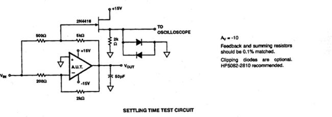
FIGURE 2-19 Large- and small-signal transient-response characteristics (Harris Semiconductors, Linear & Telecom ICs, 1994, p. 2–544)
For this particular op-amp (a Harris HA-5147), rise time is specified with an output of 200 mV and a gain of 10. thus, the small-signal response displays must be used. As shown, the rise time (measured from the 10% point to the 90% point, Figure 2-18) is about 25 ns. The data sheet specifies a typical rise time of 25 ns and a maximum of 50 ns.
Settling time is the total length of time from input-step application until the output remains within a specified error-band or point around the final value. For the HA-5147, settling time is specified with an output of 10 V and a gain of −10. Thus, the large-signal response must be used. As shown, settling time is somewhat less than 400 ns (from the start of the input, through the overshoot, and back to where the output levels to 10 V). The data sheet specifies a typical settling time of 400 ns.
From a simplified design standpoint, an increase in rise time, settling time, or overshoot lowers the frequency response and bandwidth. If the IC amplifier is used in pulse applications, excessive rise times and settling times can distort the output pulse.
2.20 Phase Shift
The phase shift between input and output of some amplifiers is not a significant design factor, but is a critical factor in others, particularly op-amps. This is because an op-amp generally uses the principle of feeding back output signals to the input. Under ideal open-loop conditions, the output should be exactly 180° out of phase with the inverting input and in phase with the noninverting input. Any substantial deviation from this condition can cause op-amp circuit problems.
For example, assume that an op-amp circuit uses the inverting input with the noninverting input grounded, and the circuit output is fed back to the inverting input. If the output is not shifted the full 180° (for example, if the shift is only a few degrees), the circuit might oscillate (because the output being fed back is almost in phase with the input). Even if there is no oscillation, the op-amp gain will not be stabilized, and the circuit will not operate properly.
A dual-trace scope, connected as shown in Fig. 2-20, is the ideal tool for phase measurement. For the most accurate results, the cables that connect the input and output should be of the same length and characteristics. At higher frequencies, a difference in cable length or characteristics can introduce a phase shift. For simplicity, adjust the scope controls until one cycle of the input signal occupies exactly nine divisions (typically 9 cm horizontally) of the screen. Then, find the phase factor of the input signal. For example, if 9 cm represents one complete cycle (360°), 1 cm represents 40° (369/9 = 40).

With the phase factor established, measure the horizontal distance between corresponding points on the two waveforms (input and output signals). Then multiply the measured distance by the phase factor of 40°/cm to find the phase difference. For example, if the horizontal distance is 0.6 cm with a 40°/cm phase factor, the phase difference is 0.6 × 40° = 24°. If the scope has speed magnification, you can get more accurate results. For example, if the sweep rate is increased 10 times, the magnified phase factor is 40°/cm = 4°/cm. Figure 2-20 shows the same signal with and without sweep magnification. With a 10 × magnification, the horizontal distance is 6 cm and the phase difference is 6 × 4 = 24°.
2.21 Feedback Measurement
Because op-amp circuits usually include feedback, it is sometimes necessary to measure feedback voltage at a given frequency with given operating conditions. The basic feedback-measurement connections are shown in Fig. 2-21. Although it is possible to measure the feedback voltage as shown in Fig. 2-21a, a more accurate measurement is made when the feedback lead is terminated in the normal operating impedance, as shown in Fig. 2-21b.

If an input resistance is used in the circuit, and this resistance is considerably lower than the IC input resistance, use the circuit-resistance value. If in doubt, measure the input impedance of the IC (Section 2.9), and terminate the feedback lead in that value (to measure open-loop feedback voltage). Remember that open-loop voltage gain must be substantially higher than the closed-loop voltage gain for most op-amp circuits to perform properly.
2.22 Input-Bias Current
Op-amp input-bias current is the average value of the two input-bias currents of the op-amp differential-input stage. In circuit design, the significance of input-bias current is that the resultant voltage drops across input resistors (such as the resistor at pin 3 of the IC in Fig. 2-1) and restrict the input common-mode voltage range at higher impedance levels. The input-bias current produces a voltage drop across the input resistors. This voltage drop must be overcome by the input signal (which can be a problem if the input signal is low and the input resistors are large).
Input-bias current can be measured using the circuit of Fig. 2-22. Any resistance value for R1 and R2 can be used, provided that the value produces a measurable voltage drop and that the resistance values are equal. A value of 1 k (with a tolerance of 1% or better) for both R1 and R2 is realistic for typical op-amps.

If it is not practical to connect a meter in series with both inputs (as shown), measure the voltage drop across R1 and R2, and calculate the input-bias current. For example, if the voltage is 3 mV across 1-k resistors, the input bias current is 3 µA. Try switching R1 and R2 to see if any difference is the result of difference in resistor values. In theory, the input-bias current should be the same for both inputs. In practice, the bias currents should be almost equal. Any great difference in input bias is the result of unbalance in the input differential amplifier of the IC, and it can seriously affect circuit operation (and it usually indicates a defective IC.)
2.23 Input-Offset Voltage and Current
Input-offset voltage is the voltage that must be applied at the input terminals to get zero output voltage, whereas input-offset current is the difference in input-bias current at the op-amp input. Offset voltage and current are usually referred back to the input because the output voltages depend on feedback.
From a design standpoint, the effect of input-offset is that the input signal must overcome the offset before an output is produced. Likewise, with no input, there is a constant shift in output level. For example, if an op-amp has a 1-mV input-offset voltage and a 1-mV signal is applied, there is no output. If the signal is increased to 2 mV, the amplifier produces only the peaks.
Input-offset voltage and current can be measured using the circuit of Fig. 2-23. As shown, the output is alternately measured with R3 shorted and with R3 in the circuit. The two output voltages are recorded as E1 (S1 closed, R3 shorted) and E2 (S1 open, R3 in the circuit).

With the two output voltages recorded, the input-offset voltage and input-offset current can be calculated using the equations of Fig. 2-23. For example, assume that R1, R2, and R3 are at the values shown, that E1 is 83 mV, and that E2 is 363 mV:

2.24 Common-Mode Rejection
As discussed in Section 1.15.2, there are many definitions for common-mode rejection. No matter what definition is used, the first step to measure CMR is to find the open-loop gain of the IC at the desired operating frequency (Section 2.4). Then connect the IC in the common-mode test circuit of Fig. 2-24. Increase the common-mode voltage (at the same frequency used for the open-loop gain test) until a measurable output is obtained. Be careful not to exceed the maximum input common-mode voltage specified in the data sheet. If no such value is available, do not exceed the normal input voltage of the IC.

To simplify the calculation, increase the input voltage until the output is at some exact value, such as the 1 mV shown. Divide this value by the open-loop gain to find the equivalent differential input signal. For example, with an open-loop gain of 100 and an output of 1 mV, the equivalent differential is: 0.001/100 = 0.00001. Now measure the input voltage that produced the 1-mV output, and divide the input by the equivalent differential to find the common-mode rejection ratio. In our example, simply find the input voltage that produces the 1-mV output and move the decimal point over five places. For example, if the output is 1 mV with a 10-V input and a gain of 100, the ratio is 0.0001. This ratio can be converted to decibels, as described in Section 2.2 (a voltage ratio of 80 dB).
2.25 Power-Supply Sensitivity (or PSRR)
Power-supply sensitivity, or PSRR, is the ratio of change in input-offset voltage to the change in power-supply voltage that produces the change. On some data sheets, the term is expressed in millivolts or microvolts per volt (mV/V or µV/V), which represents the change of input-offset voltage (in mV or µV) to a change (in volts) of the power supply. In other data sheets, the term power-supply rejection ratio (PSRR) is used instead, and is given in decibels.
No matter what it is called, the characteristic can be measured using the circuit of Fig. 2-23 (the same test circuit as for input-offset voltage). The procedure is the same as for measurement of input-offset voltage, except that the supply voltage is changed (in 1-V steps). The amount of change in input-offset voltage for a 1-V change is the power-supply sensitivity (or the PSRR). The ratio of change can be converted to dB as discussed in Section 2.2. The circuit of Fig. 2-23 can also be used when the amplifier is operated from two power supplies. One supply voltage is changed (in 1-V steps) while the other supply voltage is held constant.
2.26 Amplifier Display Problems During Test
As discussed in Section 2.13, one of the most practical ways to check amplifier performance is to display the amplifier output on a scope with square waves or pulses applied at the input. However, even though the procedure is simple, there are many practical problems in making such tests. This section summarizes the most common problems and provides practical solutions.
Figure 2-25 shows the display when the generator (square-wave or pulse) is unterminated. The result is severe ringing on the pulse edges (caused by reflections), and can be eliminated by terminating the generator cable in its characteristic impedance.

FIGURE 2-25 Display when the generator is unterminated (Linear Technology, Linear Applications Handbook, 1993, p. AN47–7)
Figure 2-26 shows the display when the generator is terminated, but with a poor-quality termination. The result is a pulse with abnormal corners. On the test bench, the best termination for 50-ohm cable is the BNC coaxial type. For PC-board use, the best termination resistors are carbon or metal-film types, with the shortest possible lead lengths. (Never use wire-wound, even the so-called noninductive types.) The ground end of a terminating resistor should be placed so that the currents flowing from the termination do not disrupt circuit operation. For example, do not return the terminator current to ground near the grounded positive input of an inverting op-amp. Typical 5-V pulses through a 50-ohm terminating resistor produce 100-mA current spikes that could upset the desired zero-volt op-amp reference.

FIGURE 2-26 Display when generator has poor-quality termination (Linear Technology, Linear Applications Handbook, 1993, p. AN47–8)
Figure 2-27 shows the display when the ground lead of scope probe is too long. Keep the probe ground connection as short as possible (preferably less than one inch for higher frequencies). If practical, use scope probes that mate directly to board-mounted coax connectors. At higher frequencies, any long ground lead looks inductive, causing the ringing shown in Fig. 2-27.

FIGURE 2-27 Display when probe ground lead is too long (Linear Technology, Linear Applications Handbook, 1993, p. AN47–8)
Figure 2-28 shows the display when the scope probe is properly grounded but is not properly compensated (or, even worse, does not match the scope characteristics). Always use the probe recommended by the scope manufacturer and check probe compensation frequently.

FIGURE 2-28 Display when probe is not properly compensated (Linear Technology, Linear Applications Handbook, 1993, p. AN47–8)
Figure 2-29 shows another display when the scope probe is too heavily compensated or is too slow for the scope. Make sure that the probe bandwidth is far greater than the measurement frequency. A typical 1X or “straight probe” has a bandwidth of 20 MHz or less and produces a large capacitive load. While on the subject of bandwidth, it is assumed that the scope bandwidth is also far greater than the highest frequency used during testing!

FIGURE 2-29 Display when probe is too heavily compensated or slow (Linear Technology, Linear Applications Handbook, 1993, p. AN47–9)
Figure 2-30 shows the display when probes at the input and output of an amplifier have different delay times. This difference in delay is added to the normal amplifier delay, and produces what appears to be excessive delay. In Fig. 2-30, the delay between the input (trace A, left side) and the output (trace B) is about 12 ns. The amplifier is supposed to have a delay of 6 ns. The apparent excess is caused by the fact that the output probe has a delay of 9 ns, with a 3 ns delay for the input probe. One way to eliminate the problem is to measure the delay of both probes and mentally factor in the difference when interpreting the display. Try connecting both probes to the same point simultaneously. Although this may not show the true delay of the probe (or the circuit), it will show the difference in delay between the probes. As a point of reference, an active probe (such as an FET probe) and a current probe can have delays of 25 ns. Delay for a fast 10X or 50-ohm probe is often less than 3 ns.

FIGURE 2-30 Display when probes have different delay times (Linear Technology, Linear Applications Handbook, 1993, p. AN47–9)
Figure 2-31 shows the display when an FET probe is overdriven. This causes what appears to be severe distortion in the amplifier. In reality, the common-mode input range of the probe is exceeded, causing the probe to overload, clip, and distort the display. In some cases, an overdriven FET probe will produce excessive delays, but without the obvious distortion. In general, do not used FET probes to monitor signal voltages greater than about ± 1 V. Use 10X and 100X attenuator probes when required.

FIGURE 2-31 Display when FET probe is overdriven (Linear Technology, Linear Applications Handbook, 1993, p. AN47–9)
Figure 2-32 shows the display when scope-probe capacitance has caused what appears to be peaking and ringing. In this case, the probe capacitance is only 10 pF, but the probe is connected to the summing point of an op-amp, causing a lag in feedback action. This forces the amplifier to overshoot and hunt as it seeks the feedback null point. The problem can be minimized by monitoring with FET probes (or other low-capacitance probes).

FIGURE 2-32 Display when probe capacitance causes peaking and ringing (Linear Technology, Linear Applications Handbook, 1993, p. AN47–10)
Figure 2-33 shows the display when the probe is not designed for wideband use. The waveform shown is the final 40 mV of a 2.5-V amplifier excursion. Instead of a sharp corner that settles cleanly, peaking occurs, followed by a long trailing decay.

FIGURE 2-33 Display when the probe is not designed for wideband use (Linear Technology, Linear Applications Handbook, 1993, p. AN47–10)
Figure 2-34 shows the display when the scope is overdriven. The waveform shown is the final movement of an amplifier output swing. By setting the scope for 1 mv/division, the purpose of the measurement is to view the settling pattern (Fig. 2-18) with high resolution. Any observation that requires off-screen positioning of the display (where only a portion of the waveform is observed) should be approached with caution. It is possible that the scope will be overdriven under extreme conditions (high resolution, time expansion, etc).

FIGURE 2-34 Display when the scope is overdriven (Linear Technology, Linear Applications Handbook, 1993, p. AN47–10)
Figure 2-35 shows the display when the amplifier circuit is without a ground plane, and is identical to the display obtained when the probe ground lead is too long (Fig. 2-27).

FIGURE 2-35 Display when amplifier circuit has no ground plane (Linear Technology, Linear Applications Handbook, 1993, p. AN47–11)
Figures 2-36 through 2-40 show the displays when the IC-amplifier power supply is not properly bypassed. This is a common problem. Bypassing is necessary to maintain low supply impedance. DC resistance and inductance in supply wires and PC traces can quickly build up to unacceptable levels. This allows the supply line to change when internal current levels of the IC change, resulting in all manner of improper operation.

FIGURE 2-36 Display when power supply is not properly bypassed (Linear Technology, Linear Applications Handbook, 1993, p. AN47–11)

FIGURE 2-37 Display when power supply is not properly bypassed, but there is no load (Linear Technology, Linear Applications Handbook, 1993, p. AN47–11)

FIGURE 2-38 Display when poor quality bypass capacitors are used (Linear Technology, Linear Applications Handbook, 1993, p. AN47–12)

FIGURE 2-39 Display when PC traces are too long between parallel capacitors (Linear Technology, Linear Applications Handbook, 1993, p. AN47–12)

FIGURE 2-40 Display when bypass capacitance value is not adequate (Linear Technology, Linear Applications Handbook, 1993, p. AN47–12)
The display in Fig. 2-36 is that of a completely unbypassed amplifier feeding a 100-ohm load. The supply seen at the IC terminals has high impedance at high frequencies. This impedance forms a voltage divider with the amplifier and load, allowing the supply to move as internal conditions change. This results in local feedback and oscillation. Figure 2-37 shows the same amplifier, but without the load. This improves the oscillation problem, but still leave unacceptable ringing and overshoot.
Figure 2-38 shows the display where poor-quality bypass capacitors are used or where the capacitors are connected too far from the IC terminals.
Figure 2-39 shows the display where capacitors are connected in parallel to get better bypassing. Although this is an acceptable practice, it must be done carefully. One common problem is where the PC traces are too long between paralleled capacitors. The capacitors and traces form a resonant circuit and produce the multiple-time-constant ringing shown in Fig. 2-39.
Figure 2-40 shows the display where good bypass capacitors are properly connected at the supply terminals of the IC, but the capacitance value is not adequate. The display of Fig. 2-40 shows the last 40 mV of a 5-V step, almost settling cleanly in 300 ns. The slight overshoot is because of a loaded (500 ohm) amplifier without quite enough bypassing. Increasing the total supply bypassing from 0.1 µF to 1 µF cured the problem. Always use large-value paralleled bypass capacitors when very fast settling is required, particularly if the amplifier is heavily loaded or sees fast load steps.
Figure 2-41 shows the display when stray capacitance (only 2 pF) at the amplifier summing point causes peaking at both the leading and trailing edges of the output waveform. This can be eliminated by proper board layout. Minimize trace area and stray capacitance at critical points in the circuit. Consider layout as an integral part of the circuit and plan accordingly.

FIGURE 2-41 Display when there is stray capacitance at the amplifier summing point (Linear Technology, Linear Applications Handbook, 1993, p. AN47–12)
Figure 2-42 shows the display when noise is getting into the circuit (say from a digital clock or switching regulator), making it appear that the amplifier output is suffering from some form of oscillation. Try to eliminate (or minimize) radiated or conducted noise signals with proper layout and shielding.

FIGURE 2-42 Display when noise is getting into the amplifier circuit (Linear Technology, Linear Applications Handbook, 1993, p. AN47–13)
Figure 2-43 shows the combined effects of stray capacitance and radiated noise. The output was taken from a gain-of-ten inverter with a 1-k input resistance. The severe peaking is induced by a 1-pF stray or parasitic capacitance across the resistor terminals, even though the input signal source is terminated in 50 ohms and provides only 20 mV of drive. This problem was cured with a ground-referred shield at a right angle to (and encircling) the 1-k resistor.

FIGURE 2-43 Display when there is stray capacitance and radiated noise (Linear Technology, Linear Applications Handbook, 1993, p. AN47–13)
Figure 2-44 shows the display when an amplifier is not compensated (no lead or lag compensation, as described in Chapter 3) and is operated with low gain (generally to increase speed). The price for the increased speed of a decompensated amplifier is a restriction on minimum allowable gain. Amplifiers without compensation are not stable below some (specified) minimum gain and can easily break into oscillation as shown. Always observe gain restrictions when using decompensated amplifiers.
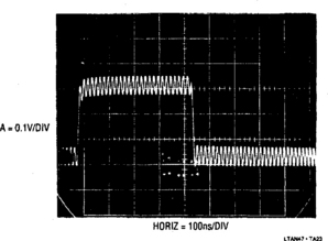
FIGURE 2-44 Display when amplifier is not compensated (Linear Technology, Linear Applications Handbook, 1993, p. AN47–13)
Figure 2-45 shows the display when there is excessive capacitive loading on an amplifier. Capacitive loading to ground introduces lag in the feedback-signal return path to the input. If enough lag is introduced (with a large capacitive load), the amplifier may oscillate as shown. Try to avoid excessive capacitive loading. If this is not practical, check the performance margins of the IC amplifier with capacitive loads.

FIGURE 2-45 Display when there is excessive capacitive loading on the amplifier (Linear Technology, Linear Applications Handbook, 1993, p. AN47–13)
Figure 2-46 shows the display when the input drive signal exceeds the common-mode input limit or range. Always keep the input inside the specified common-mode limits in all designs.

FIGURE 2-46 Display when input signal exceeds common-mode limit (Linear Technology, Linear Applications Handbook, 1993, p. AN47–14)
Figure 2-47 shows the display when an external booster circuit is placed inside the feedback loop of IC amplifier, and there are problems in the booster. In this case, the output of a unity gain inverter is apparently breaking into oscillation. In reality, the oscillation occurs in the external booster circuit and is fed back to the IC amplifier. Make certain that any external booster stages are stable before you condemn the IC amplifier. Wideband booster stages are particularly prone to high-frequency oscillation (usually caused by parasitic capacitance).
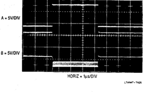
FIGURE 2-47 Display when there are problems in a booster feedback loop (Linear Technology, Linear Applications Handbook, 1993, p. AN47–14)
Figure 2-48 shows another display where oscillation is produced by an external booster. However, in this case, the booster circuit is not oscillating, but is so slow that it introduces enough lag in the feedback to produce oscillation. Make certain that booster stages are fast enough to maintain stability when placed in the feedback loop of the IC amplifier.

FIGURE 2-48 Display when there is excessive lag in a booster feedback loop (Linear Technology, Linear Applications Handbook, 1993, p. AN47–14)
Figure 2-49 shows the display when a high source impedance combines with amplifier input capacitance to band-limit the circuit. Try to minimize source impedance at levels which maintain desired bandwidth. Keep stray capacitance at the input to a minimum. Again, this goes back to good layout, both in the experimental stage and in final PC-board form.

FIGURE 2-49 Display when a high source impedance limits bandwidth (Linear Technology, Linear Applications Handbook, 1993, p. AN47–14)
Keep in mind that all the displays discussed in this section were made with a good IC amplifier, The poor results were caused by poor layout, inferior scopes and probes, incorrect (or absent) bypassing, and problems in external circuits. All these factors are discussed throughout the remainder of this book. However, it is assumed that you have a good scope and probe (both capable of displaying signals at frequencies far beyond those to be used with the amplifier circuit you are designing). The author also recommends that you read Application Note 47, by Jim Williams, in the Linear Technology 1993 Linear Applications Handbook, Volume II, for detailed information on high-speed amplifier techniques.